The Novel Thin Flexible PCB Module for 3D Packages
|
|
|
- Bethany Sybil Chapman
- 5 years ago
- Views:
Transcription
1 The Novel Thin Flexible PCB Module for 3D Packages Bo Zhang Institute of Microelectronics Chinese Academy of Sciences, Beijing, China
2 Outlines Laboratory introduction Project presentations Applications Process Reliability test Partners

 2km")
3 Bird's nest stadium The Institute of Microelectronics of Chinese Academy of Sciences PRC S PRC (P. R. China s package research center) 2km exterior IME
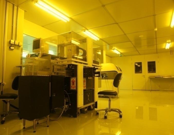
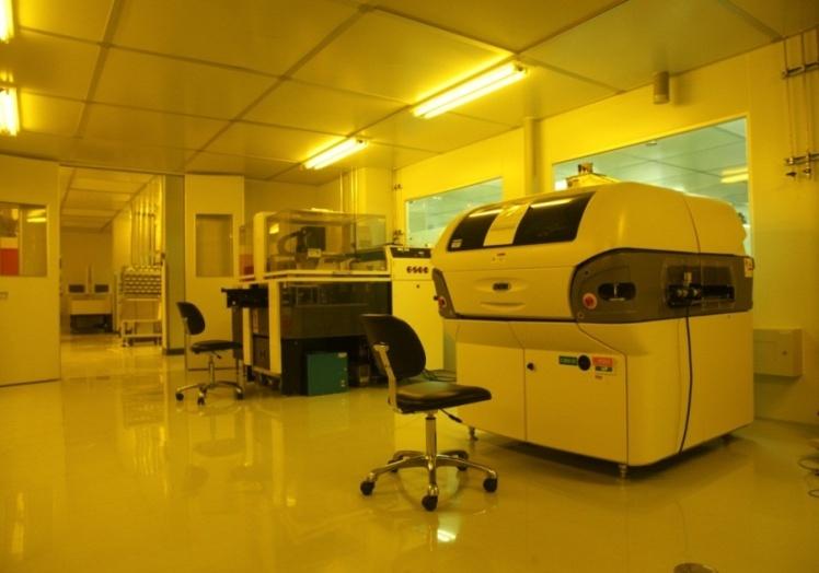
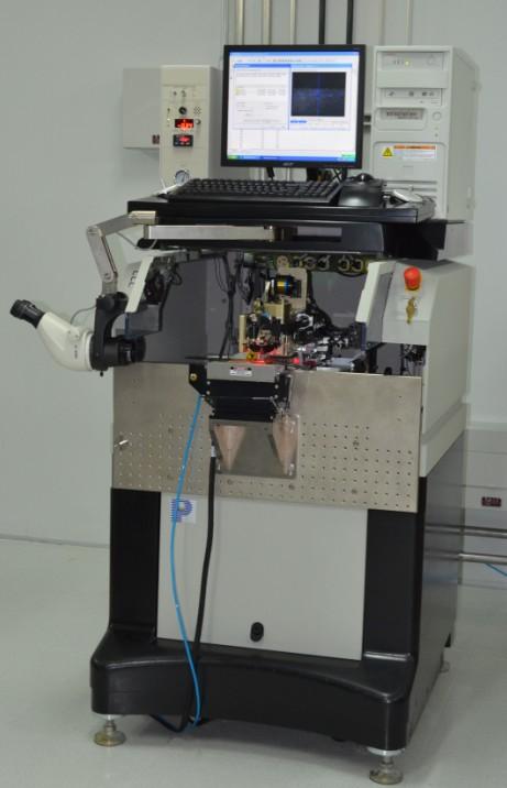
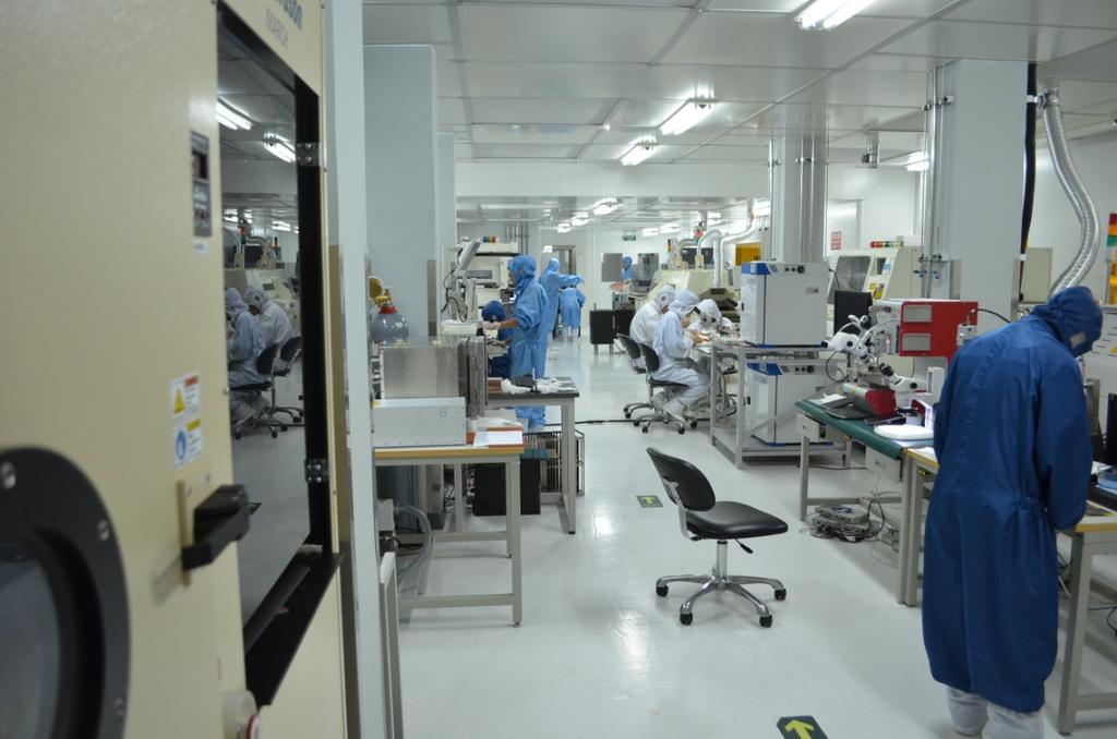
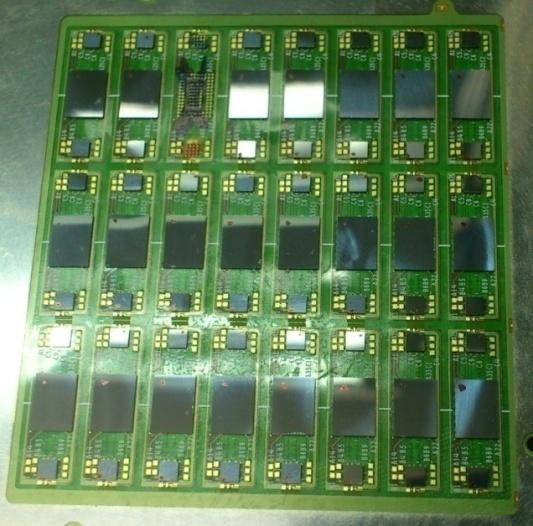
4 Technology Platform:Micro Assembly Test Line DEK printer Flip Chip Wire bonder Micro assembly area


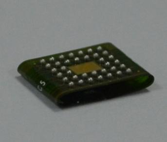
5 Applications Project presentations 5 Ultramicro cardiac pacemaker Retinal repair Press rate and depth tester Limited space of medical device makes the packaging very challenging. In this project we through flexible substrate folding accomplish chips stacking, thereby, make the electronics become light, thin, short, small to be true.
6 6 As microelectronic technology continues to evolve, medical electronics will continue to be a fast-follower of consumer electronics product platforms for the foreseeable future. Each medical device is unique and may require application-specific packaging technologies. Medical devices need a maximum of miniaturization for highest functionality in smallest volumes. Limited space of medical device makes the packaging very challenging. To meet these challenging requirements, medical original equipment manufacturers (OEMs) have been forced to develop customized packaging and assembly solutions, which are high cost. Flexible printing circuit has showed excellent advantages of electronic equipment, such as flexional, folding, three-dimensional wiring, three dimensional, and played a more and more important role in reliable miniaturization interconnection. A folded and stacked package has many advantages including an extremely thin profile. However, an additional thorny question, the bonding pads of flexible circuit substrate could be probably polluted during the encapsulation processes, which would lead to the failure of the solder ball placement.
 Encapsulation (4) Demould and ball placement Flow chart")
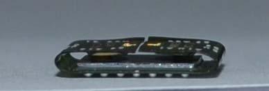
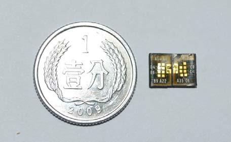
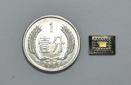
7 Process (1) Flip-chip Under fill (2) Folding and die attach (3) Encapsulation (4) Demould and ball placement Flow chart


8 3-D 封装, cont d 8 Encapsulation materials BGA ball Important bending zones Main processes: 2D package Die attach folding cured reflow Ball placement cured encapsulate reflow
9 9 Reliability test Acoustic microscopy (C-SAM) X-ray Multi-reflow (260 o C for 5 times) Auto-clave (RH 95%, 125 o C, 96 hours)


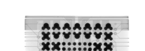
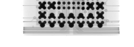
10 10 Underfill and encapsulate processes no voids be formed. To check voids, acoustic microscopy (C- SAM) was performed after underfilling process.
11 Process development-materials Before and after Multi reflow resistivity Before and after Auto clave resistivity After 260 multi reflow resistivity reduce After %RH auto clave resistivity didn t change


12 Electrical test Dc resistance test 设计与仿真模拟 A Test point on chip A C B Chip A Dc didn t change Chip B and Chip C Dc increse Bending to DC have influence

13 Microstrip line 设计与仿真模拟 BGA ball microstrip line <7GHz, didn t change <7GHz, weakening <3dB

14 Differential line 设计与仿真模拟 BGA ball side differential line <6GHz, didn t change >6GHz,after bending differential line reduce After bending,<14ghz, weakening <3dB
15 TDR 设计与仿真模拟 BGA ball TDR Bending didn t change
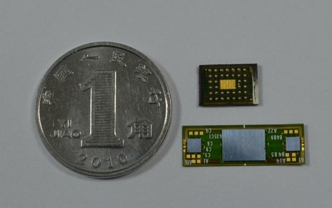
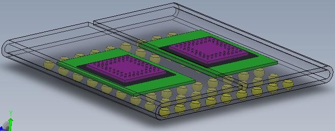
16 Samples Comparison diagram 2D folding 2D makeup Solid works model

17 Win-Win Cooperation


18 18
Sherlock Solder Models
 Introduction: Sherlock Solder Models Solder fatigue calculations in Sherlock are accomplished using one of the many solder models available. The different solder models address the type of package that
CHARACTERIZATION OF FLIP CHIP BUMP FAILURE MODES USING HIGH FREQUENCY ACOUSTIC MICRO IMAGING
 CHARACTERIZATION OF FLIP CHIP BUMP FAILURE MODES USING HIGH FREQUENCY ACOUSTIC MICRO IMAGING Janet E. Semmens and Lawrence W. Kessler SONOSCAN, INC. 530 East Green Street Bensenville, IL 60106 U.S.A. Tel:
Innovations Push Package-on-Package Into New Markets. Flynn Carson. STATS ChipPAC Inc Kato Rd Fremont, CA 94538
 Innovations Push Package-on-Package Into New Markets by Flynn Carson STATS ChipPAC Inc. 47400 Kato Rd Fremont, CA 94538 Copyright 2010. Reprinted from Semiconductor International, April 2010. By choosing
Flip Chip Installation using AT-GDP Rework Station
 Flip Chip Installation using AT-GDP Rework Station Introduction An increase in implementation of Flip Chips, Dies, and other micro SMD devices with hidden joints within PCB and IC assembly sectors requires
Features. Output Third Order Intercept (IP3) [2] dbm Power Added Efficiency %
![Features. Output Third Order Intercept (IP3) [2] dbm Power Added Efficiency %](/thumbs/84/89186722.jpg "Features. Output Third Order Intercept (IP3) [2] dbm Power Added Efficiency %") v5.1217 HMC187 2-2 GHz Typical Applications The HMC187 is ideal for: Test Instrumentation General Communications Radar Functional Diagram Features High Psat: +39 dbm Power Gain at Psat: +5.5 db High Output
v5.1217 HMC187 2-2 GHz Typical Applications The HMC187 is ideal for: Test Instrumentation General Communications Radar Functional Diagram Features High Psat: +39 dbm Power Gain at Psat: +5.5 db High Output
High Reliability and High Temperature Application Solution Solder Joint Encapsulant Paste
 High Reliability and High Temperature Application Solution Solder Joint Encapsulant Paste YINCAE Advanced Materials, LLC WHITE PAPER October 2017 2017 YINCAE Advanced Materials, LLC - All Rights Reserved.
SOLDERABLE ANISOTROPIC CONDUCTIVE ADHESIVES FOR 3D PACKAGE APPLICATIONS
 SOLDERABLE ANISOTROPIC CONDUCTIVE ADHESIVES FOR 3D PACKAGE APPLICATIONS ABSTRACT: Dr. Mary Liu and Dr. Wusheng Yin YINCAE Advanced Materials, LLC Albany, NY 3D packaging has recently become very attractive
POSSUM TM Die Design as a Low Cost 3D Packaging Alternative
 POSSUM TM Die Design as a Low Cost 3D Packaging Alternative The trend toward 3D system integration in a small form factor has accelerated even more with the introduction of smartphones and tablets. Integration
Chapter 2. Literature Review
 Chapter 2 Literature Review 2.1 Development of Electronic Packaging Electronic Packaging is to assemble an integrated circuit device with specific function and to connect with other electronic devices.
MICROELECTRONICS ASSSEMBLY TECHNOLOGIES. The QFN Platform as a Chip Packaging Foundation
 West Coast Luncheon January 15, 2014. PROMEX PROMEX INDUSTRIES INC. MICROELECTRONICS ASSSEMBLY TECHNOLOGIES The QFN Platform as a Chip Packaging Foundation 3075 Oakmead Village Drive Santa Clara CA Ɩ 95051
Characterization of Flip Chip Interconnect Failure Modes Using High Frequency Acoustic Micro Imaging With Correlative Analysis
 Characterization of Flip Chip Interconnect Failure Modes Using High Frequency Acoustic Micro Imaging With Correlative Analysis Janet E. Semmens and Lawrence W. Kessler SONOSCAN, INC. 530 East Green Street
BGA inspection and rework with HR 600/2 Failure analysis and assembly repair
 Even today some assemblies including BGA components still show soldering failures that require as a consequence to rework the BGA. The following example can be seen as a typical case for today s inspection
B. Flip-Chip Technology
 B. Flip-Chip Technology B1. Level 1. Introduction to Flip-Chip techniques B1.1 Why flip-chip? In the development of packaging of electronics the aim is to lower cost, increase the packaging density, improve
Capabilities of Flip Chip Defects Inspection Method by Using Laser Techniques
 Capabilities of Flip Chip Defects Inspection Method by Using Laser Techniques Sheng Liu and I. Charles Ume* School of Mechanical Engineering Georgia Institute of Technology Atlanta, Georgia 3332 (44) 894-7411(P)
TGP GHz 180 Phase Shifter. Primary Applications. Product Description. Measured Performance
 Amplitude Error (db) S21 (db) 10.0 9.0 8.0 7.0 6.0 5.0 4.0 3.0 2.0 1.0 Measured Performance 0.0 140 30 31 32 33 34 35 36 37 38 39 40 0-1 -2-3 -4-5 State 0-6 State 1-7 -8-9 -10 30 31 32 33 34 35 36 37 38
BGA/CSP Re-balling Bob Doetzer Circuit Technology Inc.
 BGA/CSP Re-balling Bob Doetzer Circuit Technology Inc. www.circuittechnology.com The trend in the electronics interconnect industry towards Area Array Packages type packages (BGA s, CSP s, CGA s etc.)
Analysis signal transitions characteristics of BGA-via multi-chip module Baolin Zhou1,a, Dejian Zhou1,b
 5th International Conference on Computer Sciences and Automation Engineering (ICCSAE 2015) Analysis signal transitions characteristics of BGA-via multi-chip module Baolin Zhou1,a, Dejian Zhou1,b 1 Electromechanical
Advanced Packaging Equipment Solder Jetting & Laser Bonding
 Advanced Packaging Equipment Solder Jetting & Laser Bonding www.pactech.comw.pactech.com PacTech Packaging Technologies Pioneering in laser solder jetting technologies since 1995 Our mission is to reshape
TSV MEOL (Mid-End-Of-Line) and its Assembly/Packaging Technology for 3D/2.5D Solutions
 and its Assembly/Packaging Technology for 3D/2.5D Solutions") TSV MEOL (Mid-End-Of-Line) and its Assembly/Packaging Technology for 3D/2.5D Solutions Seung Wook YOON, D.J. Na, *K. T. Kang, W. K. Choi, C.B. Yong, *Y.C. Kim and Pandi C. Marimuthu STATS ChipPAC Ltd.
TSV MEOL (Mid-End-Of-Line) and its Assembly/Packaging Technology for 3D/2.5D Solutions Seung Wook YOON, D.J. Na, *K. T. Kang, W. K. Choi, C.B. Yong, *Y.C. Kim and Pandi C. Marimuthu STATS ChipPAC Ltd.
Winter College on Optics: Fundamentals of Photonics - Theory, Devices and Applications February 2014
 2572-10 Winter College on Optics: Fundamentals of Photonics - Theory, Devices and Applications 10-21 February 2014 Photonic packaging and integration technologies II Sonia M. García Blanco University of
(12) United States Patent (10) Patent No.: US 6,387,795 B1
 United States Patent (10) Patent No.: US 6,387,795 B1") USOO6387795B1 (12) United States Patent (10) Patent No.: Shao (45) Date of Patent: May 14, 2002 (54) WAFER-LEVEL PACKAGING 5,045,918 A * 9/1991 Cagan et al.... 357/72 (75) Inventor: Tung-Liang Shao, Taoyuan
USOO6387795B1 (12) United States Patent (10) Patent No.: Shao (45) Date of Patent: May 14, 2002 (54) WAFER-LEVEL PACKAGING 5,045,918 A * 9/1991 Cagan et al.... 357/72 (75) Inventor: Tung-Liang Shao, Taoyuan
MA4L Series. Silicon PIN Limiters RoHS Compliant. M/A-COM Products Rev. V12. Features. Chip Outline. Description. Applications
 Features Low Insertion Loss and Noise Figure High Peak and Average Operating Power Various P1dB Compression Powers Low Flat Leakage Power Proven Reliable, Silicon Nitride Passivation Chip Outline A Square
2.5D Platform (Examples of products produced to date are shown here to demonstrate Amkor's production capabilities)
") Wafer Finishing & Flip Chip Stacking interconnects have emerged to serve a wide range of 2.5D- & 3D- packaging applications and architectures that demand very high performance and functionality at the
Wafer Finishing & Flip Chip Stacking interconnects have emerged to serve a wide range of 2.5D- & 3D- packaging applications and architectures that demand very high performance and functionality at the
Silicon Interposers enable high performance capacitors
 Interposers between ICs and package substrates that contain thin film capacitors have been used previously in order to improve circuit performance. However, with the interconnect inductance due to wire
Flip-Chip for MM-Wave and Broadband Packaging
 1 Flip-Chip for MM-Wave and Broadband Packaging Wolfgang Heinrich Ferdinand-Braun-Institut für Höchstfrequenztechnik (FBH) Berlin / Germany with contributions by F. J. Schmückle Motivation Growing markets
FLIP CHIP LED SOLDER ASSEMBLY
 As originally published in the SMTA Proceedings FLIP CHIP LED SOLDER ASSEMBLY Gyan Dutt, Srinath Himanshu, Nicholas Herrick, Amit Patel and Ranjit Pandher, Ph.D. Alpha Assembly Solutions South Plainfield,
TAIPRO Engineering. Speaker: M. Saint-Mard Managing director. TAIlored microsystem improving your PROduct
 TAIPRO Engineering MEMS packaging is crucial for system performance and reliability Speaker: M. Saint-Mard Managing director TAIPRO ENGINEERING SA Michel Saint-Mard Administrateur délégué m.saintmard@taipro.be
Features. Preliminary. = +25 C, IF = 1 GHz, LO = +13 dbm*
 Typical Applications Features The is ideal for: Test Equipment & Sensors Point-to-Point Radios Point-to-Multi-Point Radios Military & Space Functional Diagram Wide IF Bandwidth: DC - 17 GHz Input IP3:
SHENMAO Technology Inc. Your Ultimate Choice for Solder
 Your Ultimate Choice for Solder Company Profile TSE Code: 3305 Founded: Oct. 1973 Capital: US $40 million (2015) Revenue: US $157 million (2015) President: Mr. S. L. Lee General Manager: Mr. H. W. Lee
Thin Film Resistor Integration into Flex-Boards
 Thin Film Resistor Integration into Flex-Boards 7 rd International Workshop Flexible Electronic Systems November 29, 2006, Munich by Dr. Hans Burkard Hightec H MC AG, Lenzburg, Switzerland 1 Content HiCoFlex:
Advanced High-Density Interconnection Technology
 Advanced High-Density Interconnection Technology Osamu Nakao 1 This report introduces Fujikura s all-polyimide IVH (interstitial Via Hole)-multi-layer circuit boards and device-embedding technology. Employing
Measured Fixtured Data Bias: 40mA Isolation (db)
") 77 GHz Transceiver Switch Key Features I/O Compatible with MA4GC6772 3 Antenna Ports Receive, Source, and LO Ports 2.5 db RX/TX Insertion Loss Typical 4 db Source/Mixer Isolation Typical 25 db Ant/Ant
77 GHz Transceiver Switch Key Features I/O Compatible with MA4GC6772 3 Antenna Ports Receive, Source, and LO Ports 2.5 db RX/TX Insertion Loss Typical 4 db Source/Mixer Isolation Typical 25 db Ant/Ant
Module No. # 07 Lecture No. # 35 Vapour phase soldering BGA soldering and De-soldering Repair SMT failures
 An Introduction to Electronics Systems Packaging Prof. G. V. Mahesh Department of Electronic Systems Engineering Indian Institute of Science, Bangalore Module No. # 07 Lecture No. # 35 Vapour phase soldering
Advances in X-Ray Technology for Semicon Applications Keith Bryant and Thorsten Rother
 Advances in X-Ray Technology for Semicon Applications Keith Bryant and Thorsten Rother X-Ray Champions, Telspec, Yxlon International Agenda The x-ray tube, the heart of the system Advances in digital detectors
High Power Ka-Band SPDT Switch
 High Power Ka-Band SPDT Switch Key Features and Performance 27-46 GHz Frequency Range > 33 dbm Input P1dB @ V C = 7.5V On Chip Biasing Resistors On Chip DC Blocks < 0.9 db Typical Insertion Loss < 4ns
BOARD DESIGN, SURFACE MOUNT ASSEMBLY AND BOARD LEVEL RELIABILITY ASPECTS OF FUSIONQUAD TM PACKAGES
 BOARD DESIGN, SURFACE MOUNT ASSEMBLY AND BOARD LEVEL RELIABILITY ASPECTS OF FUSIONQUAD TM PACKAGES Ahmer Syed 1, Sundar Sethuraman 2, WonJoon Kang 1, Gary Hamming 1, YeonHo Choi 1 1 Amkor Technology, Inc.
inemi Statement of Work (SOW) Packaging TIG Primary Factors in Component Warpage
 Packaging TIG Primary Factors in Component Warpage") inemi Statement of Work (SOW) Packaging TIG Primary Factors in Component Warpage Version 3.0 Date: September 21, 2010 Project Leader: Peng Su (Cisco Systems) Co-Project Leader: inemi Coach: Jim Arnold
inemi Statement of Work (SOW) Packaging TIG Primary Factors in Component Warpage Version 3.0 Date: September 21, 2010 Project Leader: Peng Su (Cisco Systems) Co-Project Leader: inemi Coach: Jim Arnold
USING SIGNATURE IDENTIFICATION FOR RAPID AND EFFECTIVE X-RAY INSPECTION OF BALL GRID ARRAYS
 USING SIGNATURE IDENTIFICATION FOR RAPID AND EFFECTIVE X-RAY INSPECTION OF BALL GRID ARRAYS Gil Zweig Glenbrook Technologies, Inc. Randolph, New Jersey USA gzweig@glenbrooktech.com ABSTRACT Although X-ray
A Miniaturized Multi-Channel TR Module Design Based on Silicon Substrate
 Progress In Electromagnetics Research Letters, Vol. 74, 117 123, 2018 A Miniaturized Multi-Channel TR Module Design Based on Silicon Substrate Jun Zhou 1, 2, *, Jiapeng Yang 1, Donglei Zhao 1, and Dongsheng
SESUB - Its Leadership In Embedded Die Packaging Technology
 SESUB - Its Leadership In Embedded Die Packaging Technology Sip Conference China 2018 TDK Corporation ECBC, PAF, SESUB BU Kofu, Japan October 17, 2018 Contents SESUB Introduction SESUB Process SESUB Quality
Min Tao, Ph. D, Ashok Prabhu, Akash Agrawal, Ilyas Mohammed, Ph. D, Bel Haba, Ph. D Oct , IWLPC
 PACKAGE-ON-PACKAGE INTERCONNECT FOR FAN-OUT WAFER LEVEL PACKAGES Min Tao, Ph. D, Ashok Prabhu, Akash Agrawal, Ilyas Mohammed, Ph. D, Bel Haba, Ph. D Oct 18-20 2016, IWLPC 1 Outline Laminate to Fan-Out
P21BN300M5S Milli Cap
 P21BN300M5S Milli Cap Milli Cap : The "Ideal" SMT Capacitor Benefits: Increased Useable Bandwidth Very Low Series Inductance Ultra High Series Resonance Low Loss, High Q Functional Applications: Matching
Sectional Design Standard for Flexible/Rigid-Flexible Printed Boards
 Sectional Design Standard for Flexible/Rigid-Flexible Printed Boards Developed by the Flexible Circuits Design Subcommittee (D-) of the Flexible Circuits Committee (D-0) of IPC Supersedes: IPC-2223C -
An Introduction to Electronics Systems Packaging. Prof. G. V. Mahesh. Department of Electronic Systems Engineering
 An Introduction to Electronics Systems Packaging Prof. G. V. Mahesh Department of Electronic Systems Engineering Indian Institute of Science, Bangalore Module No. # 07 Lecture No. # 33 Reflow and Wave
'*+,+$&#' ' '") !"#$%&'()'*"+,+$&#' *";
!"#$%&'()'*"+,+$&#' *"; 3D TSV Micro Cu Column Chip-to-Substrate/Chip Assmbly/Packaging Technology
 3D TSV Micro Cu Column Chip-to-Substrate/Chip Assmbly/Packaging Technology by Seung Wook Yoon, *K. T. Kang, W. K. Choi, * H. T. Lee, Andy C. B. Yong and Pandi C. Marimuthu STATS ChipPAC LTD, 5 Yishun Street
Figure 1. FCBGA and fccsp Packages
 Packaging Technology and Design Challenge for Fine Pitch Micro-Bump Cu-Pillar and BOT (Direct Bond on Substrate-Trace) Using TCNCP (Thermal Compression with Non-Conductive Paste Underfill) Method *MJ (Myung-June)
Advanced SMT Laboratory and Technology Excellence Center
 Advanced SMT Laboratory and Technology Excellence Center Advanced SMT Laboratory and Technology Excellence Center Investing in science for serious returns In today s high-tech industries, knowledge makes
EUFANET Toulouse conferences, November 28th-29th, 2011 Stéphane Bellenger, IPDiA
 3D low-profile Silicon interposer using Passive Integration (PICS) and Advanced Packaging Solutions EUFANET Toulouse conferences, November 28th-29th, 2011 Stéphane Bellenger, IPDiA 3D Advanced Integration
PAGE 1/6 ISSUE Jul SERIES Micro-SPDT PART NUMBER R516 XXX 10X R 516 _ 1 0 _
 PAGE 1/6 ISSUE Jul-24-2017 SERIES Micro-SPDT PART NUMBER R516 XXX 10X R516 series: the RAMSES concept merges with the SLIM LINE technology, breaking up the frequency limits of SMT switches : - FULL SMT
Bob Willis Process Guides
 What is a Printed Circuit Board Pad? What is a printed circuit board pad, it may sound like a dumb question but do you stop to think what it really does and how its size is defined and why? A printed circuit
Novel Packaging Approaches for Miniature Antennas
 Novel Packaging Approaches for Miniature Antennas Will McKinzie, Greg Mendolia, and John Dutton Etenna Corporation 6100-C Frost Place, Laurel, MD 20707 wmckinzie@etenna.com, gmendolia@etenna.com, and jdutton@etenna.com
ACOUSTIC MICRO IMAGING ANALYSIS METHODS FOR 3D PACKAGES
 ACOUSTIC MICRO IMAGING ANALYSIS METHODS FOR 3D PACKAGES Janet E. Semmens Sonoscan, Inc. Elk Grove Village, IL, USA Jsemmens@sonoscan.com ABSTRACT Earlier studies concerning evaluation of stacked die packages
New Approaches to Develop a Scalable 3D IC Assembly Method
 New Approaches to Develop a Scalable 3D IC Assembly Method Charles G. Woychik Ph.D. Sangil Lee, Ph.D., Scott McGrath, Eric Tosaya and Sitaram Arkalgud Ph.D. Invensas Corporation 3025 Orchard Parkway San
23. Packaging of Electronic Equipments (2)
") 23. Packaging of Electronic Equipments (2) 23.1 Packaging and Interconnection Techniques Introduction Electronic packaging, which for many years was only an afterthought in the design and manufacture of
23. Packaging of Electronic Equipments (2) 23.1 Packaging and Interconnection Techniques Introduction Electronic packaging, which for many years was only an afterthought in the design and manufacture of
AMD ATI TSMC 28 nm Gate Last HKMG CMOS Process
 AMD ATI 7970 215-0821060 TSMC 28 nm Gate Last HKMG CMOS Process Package Analysis 3685 Richmond Road, Suite 500, Ottawa, ON K2H 5B7 Canada Tel: 613-829-0414 www.chipworks.com Package Analysis Some of the
A Miniaturized Wide-Band LTCC Based Fractal Antenna
 A Miniaturized Wide-Band LTCC Based Fractal Antenna Farhan A. Ghaffar, Atif Shamim and Khaled N. Salama Electrical Engineering Program King Abdullah University of Science and Technology Thuwal 23955-6500,
Considerations in High-Speed High Performance Die-Package-Board Co-Design. Jenny Jiang Altera Packaging Department October 2014
 Considerations in High-Speed High Performance Die-Package-Board Co-Design Jenny Jiang Altera Packaging Department October 2014 Why Co-Design? Complex Multi-Layer BGA Package Horizontal and vertical design
RF3932D 60W GaN on SiC Power Amplifier Die
 60W GaN on SiC Power Amplifier Die RF3932D Package: Die The RF3932D is a 48V, 60W, GaN on SiC high power discrete amplifier die designed for commercial wireless infrastructure, cellular and WiMAX infrastructure,
!"#$"%&' ()#*+,-+.&/0(
#*+,-+.&/0(") !"#$"%&' ()#*+,-+.&/0( Multi Chip Modules (MCM) or Multi chip packaging Industry s first MCM from IBM. Generally MCMs are horizontal or two-dimensional modules. Defined as a single unit containing two
!"#$"%&' ()#*+,-+.&/0( Multi Chip Modules (MCM) or Multi chip packaging Industry s first MCM from IBM. Generally MCMs are horizontal or two-dimensional modules. Defined as a single unit containing two
Handling and Processing Details for Ceramic LEDs Application Note
 Handling and Processing Details for Ceramic LEDs Application Note Abstract This application note provides information about the recommended handling and processing of ceramic LEDs from OSRAM Opto Semiconductors.
Analog Devices Welcomes Hittite Microwave Corporation NO CONTENT ON THE ATTACHED DOCUMENT HAS CHANGED
 Analog Devices Welcomes Hittite Microwave Corporation NO CONTENT ON THE ATTACHED DOCUMENT HAS CHANGED www.analog.com www.hittite.com Report Title: Report Type: Date: Qualification Test Report See Attached
Silicon Photonics for Mid-Board Optical Modules Marc Epitaux
 Silicon Photonics for Mid-Board Optical Modules Marc Epitaux Chief Architect at Samtec, Inc Outline Interconnect Solutions Mid-Board Optical Modules Silicon Photonics o Benefits o Challenges DragonFly
Acoustic microscopy for 3D-SiP failure analysis
 Acoustic microscopy for 3D-SiP failure analysis Peter Czurratis PVA TePla Analytical Systems GmbH, Westhausen, Germany Sebastian Brand Fraunhofer Center for Applied Microstructure Diagnostics (CAM) Halle,
MASW P. SURMOUNT PIN Diode Switch Element with Thermal Terminal. Features. Description. Ordering Information 2.
 Features Specified Bandwidth: 45MHz 2.5GHz Useable 30MHz to 3.0GHz Low Loss 40dB High C.W. Incident Power, 50W at 500MHz High Input IP3, +66dBm @ 500MHz Unique Thermal Terminal for
Application Note AN-1011
 AN-1011 Board Mounting Application Note for 0.800mm Pitch Devices For part numbers IRF6100, IRF6100PBF, IR130CSP, IR130CSPPBF, IR140CSP, IR140CSPPBF, IR1H40CSP, IR1H40CSPPBF By Hazel Schofield and Philip
Enabling concepts: Packaging Technologies
 Enabling concepts: Packaging Technologies Ana Collado / Liam Murphy ESA / TEC-EDC 01/10/2018 ESA UNCLASSIFIED - For Official Use Enabling concepts: Packaging Technologies Drivers for the future: Higher
Source: Nanju Na Jean Audet David R Stauffer IBM Systems and Technology Group
 Title: Package Model Proposal Source: Nanju Na (nananju@us.ibm.com) Jean Audet (jaudet@ca.ibm.com), David R Stauffer (dstauffe@us.ibm.com) Date: Dec 27 IBM Systems and Technology Group Abstract: New package
Two major features of this text
 Two major features of this text Since explanatory materials are systematically made based on subject examination questions, preparation
Texas Instruments X66AK2E05XABD25 Multi-Core DSP + ARM KeyStone II SoC
 Texas Instruments X66AK2E05XABD25 Multi-Core DSP + ARM KeyStone II SoC Basic Package Analysis 1891 Robertson Road, Suite 500, Ottawa, ON K2H 5B7 Canada Tel: 613-829-0414 chipworks.com Basic Package Analysis
Flip Chip Assembly on PCB Substrates with Coined Solder Bumps
 Flip Chip Assembly on PCB Substrates with Coined Solder Bumps Jae-Woong Nah, Kyung W. Paik, Soon-Jin Cho*, and Won-Hoe Kim* Department of Materials Sci. & Eng., Korea Advanced Institute of Science and
NEW PACKAGING AND INTERCONNECT TECHNOLOGIES FOR ULTRA THIN CHIPS
 NEW PACKAGING AND INTERCONNECT TECHNOLOGIES FOR ULTRA THIN CHIPS Christine Kallmayer and Rolf Aschenbrenner Fraunhofer IZM Berlin, Germany kallmayer@izm.fhg.de Julian Haberland and Herbert Reichl Technical
PRESS KIT. High Accuracy Device Bonder with Robotics.
 PRESS KIT High Accuracy Device Bonder with Robotics Press Announcement SET Introduces FC300R High Accuracy Device Bonder with Robotics FC300R: an Easy-to-Use Production Platform Ideal for High Accuracy
- 01dB = 1dB, - 02dB = 2dB, - 03dB = 3dB, - 04dB = 4dB, - 05dB = 5dB, - 06dB = 6dB, - 07dB = 7dB, - 08dB = 8dB, - 09dB = 9dB, - 10dB = 10dB
 AT02M0.09 - Page 1 of 13 Product Family: Part Number Series: Temperature Variable Attenuators ATV112F Series Construction: High purity Alumina Substrate Thermo-sensitive thermistor Ni alloy thin-film resistive
EOTPR Customer Case Studies. EUFANET Workshop: Findings OPEN?
 EOTPR Customer Case Studies EUFANET Workshop: Findings OPEN? OUTLINE o EOTPR introduction basic scheme o EOTPR OPEN customer case studies o Open on BGA trace (evaluation) o Open on embedded BGA trace o
TechSearch International, Inc. Corporate Overview E. Jan Vardaman, President
 TechSearch International, Inc. Corporate Overview E. Jan Vardaman, President Corporate Background Founded in 1987 and headquartered in Austin, Texas Recognized around the world as a leading consulting
Extending Acoustic Microscopy for Comprehensive Failure Analysis Applications
 Extending Acoustic Microscopy for Comprehensive Failure Analysis Applications Sebastian Brand, Matthias Petzold Fraunhofer Institute for Mechanics of Materials Halle, Germany Peter Czurratis, Peter Hoffrogge
4 Watt Ka-Band HPA Key Features Measured Performance Primary Applications Ka-Band VSAT Product Description
 4 Watt Ka-Band HPA Key Features Frequency Range: 28-31 GHz 3 dbm Nominal Psat Gain: 24 db Return Loss: -8 db Bias: Vd = V, Idq = 1. A, Vg = -.75 V Typical Technology: 3MI.15 um Power phemt Chip Dimensions:
Design and Assembly Process Implementation for BGAs
 Design and Assembly Process Implementation for BGAs Developed by the Device Manufacturers Interface Committee of IPC Supersedes: IPC-7095A - October 2004 IPC-7095 - August 2000 Users of this publication
High efficient heat dissipation on printed circuit boards
 High efficient heat dissipation on printed circuit boards Figure 1: Heat flux in a PCB Markus Wille Schoeller Electronics Systems GmbH www.schoeller-electronics.com Abstract This paper describes various
X-ray Inspection Systems 2D AXI / 3D AXI / WAXI
 X-ray Inspection Systems 2D AXI / 3D AXI / WAXI SMT / Semiconductor Analysis Equipment High-performance X-ray Inspection System X-eye SF160 Series Non-destructive analysis of semiconductor, SMT, and electron/electric
A Study on Package Stacking Process for Package-on-Package (PoP)
") A Study on Package Stacking Process for Package-on-Package (PoP) Akito Yoshida, Jun Taniguchi, *Katsumasa Murata, *Morihiro Kada, **Yusuke Yamamoto, ***Yoshinori Takagi, ***Takeru Notomi, ***Asako Fujita
A Study on Package Stacking Process for Package-on-Package (PoP) Akito Yoshida, Jun Taniguchi, *Katsumasa Murata, *Morihiro Kada, **Yusuke Yamamoto, ***Yoshinori Takagi, ***Takeru Notomi, ***Asako Fujita
23-29 GHz High Power Amplifier TGA9070-SCC
 23-29 GHz High Power Amplifier TGA9070-SCC Description The TriQuint TGA9070-SCC is a three stage HPA MMIC design using TriQuint s proven 0.25 um Power phemt process to support a variety of millimeter wave
12-18 GHz Ku-Band 3-Stage Driver Amplifier TGA2507
 12- GHz Ku-Band 3-Stage Driver Amplifier Key Features 12- GHz Bandwidth 28 db Nominal Gain dbm P1dB Bias: 5,6,7 V, 80 ± 10% ma Self Bias 0.5 um 3MI mmw phemt Technology Chip Dimensions: 1.80 x 0.83 x 0.1
!"#$%&'()'*"+,+$&#' ' '
'*+,+$&#' ' '") !"#$%&'()'*"+,+$&#' *"89"+&+6'B22&83%45'8/6&10/%2'A"1'/22&83%4'/+#'C"0+0+D'8&67"#2'0+'&%&
!"#$%&'()'*"+,+$&#' *"89"+&+6'B22&83%45'8/6&10/%2'A"1'/22&83%4'/+#'C"0+0+D'8&67"#2'0+'&%&
BGA (Ball Grid Array)
") BGA (Ball Grid Array) National Semiconductor Application Note 1126 November 2002 Table of Contents Introduction... 2 Package Overview... 3 PBGA (PLASTIC BGA) CONSTRUCTION... 3 TE-PBGA (THERMALLY ENHANCED
BGA (Ball Grid Array) National Semiconductor Application Note 1126 November 2002 Table of Contents Introduction... 2 Package Overview... 3 PBGA (PLASTIC BGA) CONSTRUCTION... 3 TE-PBGA (THERMALLY ENHANCED
High Power DC - 18GHz SPDT FET Switch
 High Power DC - 18GHz SPDT FET Switch Key Features and Performance DC - 18 GHz Frequency Range 29 dbm Input P1dB @ V C = -5V > 30 db Isolation
Powerchip Semiconductor Corporation A3R12E3GEF G6E 635BLC4M 512 Megabit DDR2 SDRAM Structural Analysis
 February 23, 2007 Powerchip Semiconductor Corporation A3R12E3GEF G6E 635BLC4M Structural Analysis For comments, questions, or more information about this report, or for any additional technical needs concerning
IMPROVED SMT AND BLR OF 0.35MM PITCH WAFER LEVEL PACKAGES
 As originally published in the SMTA Proceedings. IMPROVED SMT AND BLR OF 0.35MM PITCH WAFER LEVEL PACKAGES Brian Roggeman and Beth Keser Qualcomm Technologies, Inc. San Diego, CA, USA roggeman@qti.qualcomm.com
AND8081/D. Flip Chip CSP Packages APPLICATION NOTE
 Flip Chip CSP Packages Prepared by: Denise Thienpont ON Semiconductor Staff Engineer APPLICATION NOTE Introduction to Chip Scale Packaging This application note provides guidelines for the use of Chip
Glenbrook presents the RTXfamily: innovative, affordable, upgradable
 Glenbrook presents the RTXfamily: innovative, affordable, upgradable Real-time X-ray inspection systems from the desktop to the production line. Glenbrook Technologies' tradition of innovation in X-ray
The Advantages of Integrated MEMS to Enable the Internet of Moving Things
 The Advantages of Integrated MEMS to Enable the Internet of Moving Things January 2018 The availability of contextual information regarding motion is transforming several consumer device applications.
27-31 GHz 1W Power Amplifier TGA4509-EPU
 27-31 GHz 1W Power Amplifier Key Features 22 db Nominal Gain @ 30 GHz 30 dbm Nominal Pout @ P1dB 25% PAE @ P1dB -10 db Nominal Return Loss Built-in Power Detector 0.25-µm mmw phemt 3MI Bias Conditions:
TGL GHz Voltage Variable Attenuator
 Applications Commercial and Military Radar Electronic Warfare Satellite Communications Point to Point Radio Instrumentation General Purpose Product Features Functional Block Diagram Frequency Range: 2
MemsTech MSM3C-S4045 Integrated Silicon Microphone with Supplementary TEM Analysis
 MemsTech MSM3C-S4045 Integrated Silicon Microphone with Supplementary TEM Analysis MEMS Process Review For comments, questions, or more information about this report, or for any additional technical needs
ENGAT00000 to ENGAT00010
 Wideband Fixed Attenuator Family, DIE, DC to 50 GHz ENGAT00000 / 00001 / 00002 / 00003 / 00004 / 00005 / 00006 / 00007 / 00008 / 00009 / 00010 Typical Applications ENGAT00000 to ENGAT00010 Features Space
TGA4532 K-Band Power Amplifier
 Applications Point-to-Point Radio Communication Product Features Functional Block Diagram Frequency Range: 17.5 20 GHz Power: 32.5 dbm Psat, 31.5 dbm P1dB Gain: 23 db TOI: 43 dbm @ 22 dbm SCL Return Loss:
Laminate Based Fan-Out Embedded Die Technologies: The Other Option
 Laminate Based Fan-Out Embedded Die Technologies: The Other Option Theodore (Ted) G. Tessier, Tanja Karila*, Tuomas Waris*, Mark Dhaenens and David Clark FlipChip International, LLC 3701 E University Drive
Advanced Packaging - Pulsed-laser Heating for Flip Chip Assembly
 Page 1 of 5 Pulsed-laser Heating for Flip Chip Assembly A stress-free alternative By Thorsten Teutsch, Ph.D., Pac Tech USA, Elke Zakel, Ph.D., and Ghassem Azdasht, Pac Tech GmbH As flip chip applications
2.4 GHz SMD On-Ground Antenna
 2.4 GHz SMD On-Ground Antenna Mads Sager Antenna Technology Manager Commercial Products Division Template 2.2 Featuring high performance levels and easy integration to satisfy the demands of the wireless