TSEK38: Radio Frequency Transceiver Design Lecture 7: Receiver Synthesis (II)
|
|
|
- Gavin Morrison
- 5 years ago
- Views:
Transcription
1 TSEK38: Radio Frequency Transceiver Design Lecture 7: Receiver Synthesis (II) Ted Johansson, ISY
2 Systematic Receiver Synthesis (II) 4.3 Intermodulation characteristics Phase noise degradation 4.5 Adjacent and alternate channel selectivity Interference blocking Channel filter 4.6 Receiver Dynamic Range and AGC DR and ADC 4.7 System Design Basic aspects Requirements, key devices Performance evaluation 2
3 Phase noise and spur degradation 3 Phase noise (P) and spurious emissions (SP) from LO contaminate the signal. Will increase the IIPx,min. Intermodulation interference tones will mix with the LO P and/or SP and generate in-band noise and spurs, which degrades the CR. Covered by other : P + Sp <= other I in I in P(Δf) = P(2Δf)+6dB Δf = n BW -6 db/oct Δf Δf
4 Phase noise and spur degradation 4 P( f) = average P density over Rx BW at offset f P( Δf ) = P ( Δf ) log BW Iin [dbc/hz] P P dbm/hz P Sp = = P ( Δf ) + Iin + log BW Sp ( Δf ) + I + + (2Δf ) + I In practice, we set Sp P in Sp P (2Δf ) + Iin + log BW in I in I in -6dB/oct P(Δf) = P(2Δf)+6dB Δf = n BW Δf Δf
5 5 Phase noise estimation in two-tone test P + P + Sp Sp dbm 2 = 2 P ( Δf ) + Iin + log BW P ( Δf ) + Iin + log BW in P (2Δf ) + Iin + log BW 6dB P ( Δf ) + Iin + log BW = log 2.5 = P( Δf ) + I + log BW + 4dB P(Δf) = P(2Δf)+6dB Other dbm Sp P 1 P ( Δf P ( Δf ) Other dbm I in = log BW 4dB ) 129 dbc/hz Δf with 6 db margin From this, the impact on IIP3 can be calculated (eq ).
6 Phase noise estimation, IP2/Blocking test 6 SR budget under IP2 test (homodyne Rx). P+SP + TX,SM other The contribution by Tx leakage and self modulation is estimated to -7 dbm in this example (FDD). +6 db is equivalent to 2x2 Pn (P of 2 tones and 2x for LO spurs). 2-30dBm = -27dBm Iin Iin P + Sp dbm P ( f P ( f off off ) + ( I Other dbm log + 3dB) + log BW in ) 138dBm 7dBm = 1dBm + 3dB 1dBm For foff >> Δf the P approx. the same P + Sp 2 P ( f off f off ) + I in + 3dB+ logbw
7 4.5.3 Two-tone blocking 7 Usually IP2 test not defined by standards. Instead, blockers are specified, which can be considered as IP2 test. P Bl P Bl -3dB P Bl -3dB P IM2 f off f Bl f off f Bl P + Sp 2 P ( f off ) + P Bl + logbw P IM2 dbm = 2(P Bl 3) IIP 2,Rx (two-tone model)
8 Two-tone blocking 8 Usually, maximum blocker power larger than power in two-tone test. Hence, IP2 and P would be dictated by the maximum blocker rather than by a two-tone test. oise + Distortion budget: P IM 2 + P + Sp = ( S Pin / ) min F Rx ref Other Tradeoff between IP2 and the performance of LO Can present self-mixing of blocker or for FDD also Tx leakage effects (isolation on chip must be carefully considered)
9 9 4.5 Adjacent and alternate channel selectivity Adj and alt channel selectivity measures a receiver s ability to receive a desired signal in the presence of adjacent/alternate channel signals at a given frequency offset. (modulated) Blocking characteristics measures the same but in other channels/frequencies than the adjacent/alternate channel. (CW) Determined either by: receiver filter phase noise and spurs from LO in the adj/alt channels or around the interferer. The interference signal mixes with P and spurs, generated in-band noise and spurs, which degrades the CR.
10 Adjacent and alternate channel selectivity Desired signal level for blocking test is usually defined as 3 db above the reference sensitivity level Smin,ref But differently defined for adj/alt channel selectivity and also varies between different mobile systems. Ex: WCDMA, adj channel sel: 14 db above ref.sensitivity = dbm. Allowed degradation of the allowed signal:
11 11 Adjacent and alternate channel selectivity ΔS is defined by the blocking profile and we must verify that the P + spurious contribution by adj/ alt channel does not violate SR min def ΔS Adj +15dB +50dB 2 Alternatively, we estimate how large P + spurious for adj/alt channel can be. P ΔS ΔS = Adj I f RF in = S in ( S / ) min = IM and self-mixing P + Sp + ref FRx I Adj in S in can be neglected here P + Sp = 2 P + I in + log BW P + Sp = P + Iin + log BW + 3dB dbm
12 I Adjacent and alternate channel selectivity in S SRmin 174+ log BW + = log = 94.6 P 61 3 = P in F Rx P log BW 3dB Sin 12 I in = -38 dbm S in = -86 dbm BW = 1.25 MHz SR min = 8 db F Rx = db I I Adj Alt = P ( BW ) = P (2BW ) and also I I Adj Alt = 86dBm + ΔS = 86dBm + ΔS Adj Alt Assume: P(5 MHz) -135 dbc/hz (5 MHz = 4BW) (2 octaves) P drops 6 db/oct P(BW) = -123 dbc/hz P(2BW) = -129 dbc/hz There is much reserve on adj/alt channel selectivity ΔS ΔS Adj Alt = 53.4 db = 59.4 db while ΔS ΔS def Adj def Alt = 15dB = 50dB
13 13 Adjacent and alternate channel selectivity Adj/alt channel selectivity or the blocking characteristics: Example in book (AMPS): Smin = -120 dbm, ΔSadj = 41.5 db, ΔSalt = 68.5 db. Cf. requirements: Sadj > 16 db, Salt > 60 db.

14 4.6 Receiver Dynamic Range and AGC 14 DR = range at antenna port when BER is acceptable. Lower limit = sensitivity, upper limit = allowed maximum input power.
15 Receiver Dynamic Range and AGC 15 Automatic Gain Control (AGC) is needed to cover the full DR. AGC is usually > DR. E.g. CDMA >79 db, AGC range may need 0 db. Also handles gain variations because of processing deviations, temperature, supply voltage. AGC is mainly in the digital domain, but also in the LA, IF-VGA, and BB-VGA.
16 Receiver Dynamic Range and AGC 16
17 Receiver Dynamic Range and AGC 17 RF and IF gain control can be made by stepping the LA and IF-VGA gain. Low number of gain steps, typically three steps for the LA. Hysteresis (typically 3 db) is used to avoid gain switch back and forth, causing IMD products or other interferences.
18 Receiver Dynamic Range and AGC 18 The total gain variation of the LA and IF-VGA must cover the receiver DR, gain variation over temperature, processing, frequency, and some margin. ACG control range: GCRRx > Smax - Smin - ΔGR,T + ΔGR,process + ΔGR,f + margin GR,T = gain variation due to temperature GR,process = gain variation due to device processing GR,f = gain variation due to frequency
19 RX gain and AGC 19 Gain depends on ADC voltage range Vrange. Assume V range = 1.5 V, S in,min = -92 dbm, S in,max = -15 dbm 3 2 V in, pp Sin = log = 20logVin, pp + 4dB 8R0 1mW Sin,max = -15 dbm +6 db margin for PAR and gain variations = -9 dbm 20log Vin,pp = -13 dbv (max) AV, min = 20 logvrange 20logVin, pp 16. 5dB While for minimum input signal: A V,max = 20 logvrange 20logVin, min ΔA ΔA = 99.5dB ΔA AGC = A V,max - A V,min = 83 db - ΔA ΔA = gain control of the IF-VGA (continuous)
20 RX gain and AGC 20 Various scenarios possible. Suppose we use AGC = 4 x 17 db + 15 db - ΔA (by simple gain stepping) ΔA = 15 db => AV,max = AV,min + AGC = db dbv V ADC Δ A V,max 3.5-Δ Δ-17 A V,min Hysteresis 3 db V in dbv
21 Channel Filter 21 IF In-band blockers attenuated BPF/LPF ADC Channel selection can be completed in BB but ADC must sustain the blockers I bl A(f bl ) G LPF LPF for Zero-IF +15dB +40dB +60dB A 3 (2 nd Alt) 12 db/oct / 2 ord 18 db/oct / 3 ord 24 db/oct / 4 ord f C Blocking profile (For S in = S in,min +3dB any blocker cannot overload ADC) BW /2 3BW/2 5BW/2 7BW/2 Wanted Adjacent Alternate 2nd Alternate
22 Channel Filter 22 Filter attenuation: fbl A ( fbl ) n 20log, ( fbl >> ft ) f T Blocking profile: Use simple filter (n=2). ADC must maintain the max blocker and SRmin. Trade-off between filter order and ADC resolution. k BW ( 93dBV + ΔSk ) n 20log BW / 2 93dBV + ΔS n (6 + 20logk) k SR min +8dB (*) +29dB +21dB +24dB (*) The formula works well for larger k values when the filter ch-c is compliant with the linear approximation 0
23 4.6.3 DR and ADC 23 DR = maximum effective signal-to-(noise+distortion) Requirements set by: AGC range and step size min CR ratio in-channel band noise/interference to quantization noise PAR DC offset Fading margins Filtering (e.g. close-in interferer) Architecture dependent
24 DR and ADC 24 CDMA (DL): PAR = Q-noise = 12 db below in-channel-band noise min CR = -1 db (Spread Spectrum can have CR < 0 db) fading margin = 3 db => DR = 24 db GSM (superheterodyne) Q-noise = 16 db below in-channel-band noise DC offset: 4 db margin min CR = 8 db fading margins = 20 db => DR = 48 db
25 DR and ADC 25 DR can also be expressed in EOB CDMA: 4 bits, GSM: 8 bits, TDMA (similar to GSM): bits, EDGE: bits. More advanced calculations of ADC DR and EOB: TSEK38_2018_L7_calculations_additionalslides.pdf in the Lectures folder, course page. ADC F pp
26 4.7 System Design, Basic aspects 26 Good electrical performance, lower power consumption, low cost, small size. Trade-off between a lot of parameters, e.g. higher linearity costs more current. Highest performance is probably too good! Receiver terminal: sensitivity, intermodulation, channel selectivity, blocking, spurious emissions. Minimum requirements set by standards, with certain margins, typ. 3 db at RT and 1.5 db at max temp. frequency, voltage. Sensitivity 4-5 db, intermodulation 4 db,
27 Basic aspects 27 Power consumption will directly affect the operation time of a terminal. The PA is the most power hungry component. Architecture selection: Direct conversion and low-if less costly and smaller size than superheterodyne. Superheterodyne may have better performance. Fewer parts, higher integration, more standard parts, ICs costly in low volumes.
28 Basic aspects 28 Start with choosing a receiver architecture Fundamental receiver block diagram is developed Most important components to choose: RF BPF, RF LA, RF downconverter, UHF LO synthesizer, BB amps, BB LPF, ADC. Additional components for superheterodyne: IF filters, amplifiers, I/Q down-converter, VHF LO. All components have characteristics and must be defined to work together to achieve the full receiver specification. Link budget
29 Basic requirements on key devices Filters Center frequency Bandwidth Insertion loss Ripple Group delay Rejection Input/output impedance Input/output return loss oise figure (IIP3 usually very high)
30 Basic requirements on key devices LA Frequency Gain oise figure IIP3 Reverse isolation Input/output impedance Input/output return loss
31 Basic requirements on key devices Down-Converter and I/Q Demodulator Frequency Conversion loss/gain oise Figure IIP3 IIP2 (direct-conversion) Isolation between different ports RF/IF/LO LO power Input/output impedance Input/output return loss + for I/Q: gain and phase imbalance between output ports
32 Basic requirements on key devices IF and BB amplifiers Similar to LA, but usually less stringent, especially the BB amps IF-VGA: usually continuous adjustable BB-VGA: usually step-controlled Synthesized LO Frequency Output power PLL: phase noise, spurious. Inband and out of band Settling time
33 4.7.3 Performance evaluation Line-up analysis 33 Dup /BPF LA BPF RFA BPF /LPF IFA /BBA ADC For full-duplex LO Some specs already known: Duplexer/switch loss (F) RF BPF loss (F) IP2 of downconversion mixer Mixer gain, if passive BW of filters Distribution of G, F, IIP3, (IIP2)?
34 Performance evaluation 34 p. 297
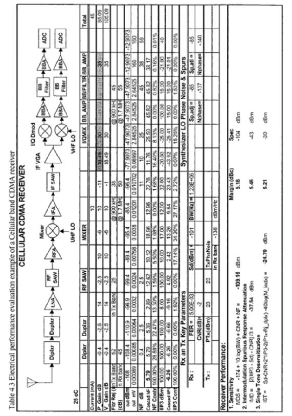
35 35

36 In the project work, more like this 36 From calculations:
37
TSEK38: Radio Frequency Transceiver Design Lecture 6: Receiver Synthesis (I)
") TSEK38: Radio Frequency Transceiver Design Lecture 6: Receiver Synthesis (I) Ted Johansson, ISY ted.johansson@liu.se Systematic Receiver Synthesis (1) 4.1 Introduction 4. Sensitivity, Noise Figure Receiver
TSEK38: Radio Frequency Transceiver Design Lecture 6: Receiver Synthesis (I) Ted Johansson, ISY ted.johansson@liu.se Systematic Receiver Synthesis (1) 4.1 Introduction 4. Sensitivity, Noise Figure Receiver
TSEK38 Radio Frequency Transceiver Design: Project work B
 TSEK38 Project Work: Task specification A 1(15) TSEK38 Radio Frequency Transceiver Design: Project work B Course home page: Course responsible: http://www.isy.liu.se/en/edu/kurs/tsek38/ Ted Johansson (ted.johansson@liu.se)
ELEN 701 RF & Microwave Systems Engineering. Lecture 4 October 11, 2006 Dr. Michael Thorburn Santa Clara University
 ELEN 7 RF & Microwave Systems Engineering Lecture 4 October, 26 Dr. Michael Thorburn Santa Clara University Lecture 5 Receiver System Analysis and Design, Part II Key Parameters Intermodulation Characteristics
ELEN 701 RF & Microwave Systems Engineering. Lecture 2 September 27, 2006 Dr. Michael Thorburn Santa Clara University
 ELEN 701 RF & Microwave Systems Engineering Lecture 2 September 27, 2006 Dr. Michael Thorburn Santa Clara University Lecture 2 Radio Architecture and Design Considerations, Part I Architecture Superheterodyne
TSEK38: Radio Frequency Transceiver Design Lecture 3: Superheterodyne TRX design
 TSEK38: Radio Frequency Transceiver Design Lecture 3: Superheterodyne TRX design Ted Johansson, ISY ted.johansson@liu.se 2 Outline of lecture 3 Introduction RF TRX architectures (3) Superheterodyne architecture
Receiver Architecture
 Receiver Architecture Receiver basics Channel selection why not at RF? BPF first or LNA first? Direct digitization of RF signal Receiver architectures Sub-sampling receiver noise problem Heterodyne receiver
RADIO RECEIVERS ECE 3103 WIRELESS COMMUNICATION SYSTEMS
 RADIO RECEIVERS ECE 3103 WIRELESS COMMUNICATION SYSTEMS FUNCTIONS OF A RADIO RECEIVER The main functions of a radio receiver are: 1. To intercept the RF signal by using the receiver antenna 2. Select the
TSEK02: Radio Electronics Lecture 8: RX Nonlinearity Issues, Demodulation. Ted Johansson, EKS, ISY
 TSEK02: Radio Electronics Lecture 8: RX Nonlinearity Issues, Demodulation Ted Johansson, EKS, ISY 2 RX Nonlinearity Issues, Demodulation RX nonlinearities (parts of 2.2) System Nonlinearity Sensitivity
ELEN 701 RF & Microwave Systems Engineering. Lecture 8 November 8, 2006 Dr. Michael Thorburn Santa Clara University
 ELEN 701 RF & Microwave Systems Engineering Lecture 8 November 8, 2006 Dr. Michael Thorburn Santa Clara University System Noise Figure Signal S1 Noise N1 GAIN = G Signal G x S1 Noise G x (N1+No) Self Noise
Session 3. CMOS RF IC Design Principles
 Session 3 CMOS RF IC Design Principles Session Delivered by: D. Varun 1 Session Topics Standards RF wireless communications Multi standard RF transceivers RF front end architectures Frequency down conversion
Introduction to Receivers
 Introduction to Receivers Purpose: translate RF signals to baseband Shift frequency Amplify Filter Demodulate Why is this a challenge? Interference Large dynamic range required Many receivers must be capable
TSEK02: Radio Electronics Lecture 8: RX Nonlinearity Issues, Demodulation. Ted Johansson, EKS, ISY
 TSEK02: Radio Electronics Lecture 8: RX Nonlinearity Issues, Demodulation Ted Johansson, EKS, ISY RX Nonlinearity Issues: 2.2, 2.4 Demodulation: not in the book 2 RX nonlinearities System Nonlinearity
Interference Issues between UMTS & WLAN in a Multi-Standard RF Receiver
 Interference Issues between UMTS & WLAN in a Multi-Standard RF Receiver Nastaran Behjou, Basuki E. Priyanto, Ole Kiel Jensen, and Torben Larsen RISC Division, Department of Communication Technology, Aalborg
RF Receiver Hardware Design
 RF Receiver Hardware Design Bill Sward bsward@rtlogic.com February 18, 2011 Topics Customer Requirements Communication link environment Performance Parameters/Metrics Frequency Conversion Architectures
26.8: A 1.9GHz Single-Chip CMOS PHS Cellphone
 26.8: A 1.9GHz Single-Chip CMOS PHS Cellphone William W. Si, Srenik Mehta, Hirad Samavati, Manolis Terrovitis, Michael Mack, KeithOnodera, SteveJen, Susan Luschas, Justin Hwang, SuniMendis, DavidSu, BruceWooley
Radio Receiver Architectures and Analysis
 Radio Receiver Architectures and Analysis Robert Wilson December 6, 01 Abstract This article discusses some common receiver architectures and analyzes some of the impairments that apply to each. 1 Contents
Receiver Architectures
 83080RA/1 Receiver Architectures Markku Renfors Tampere University of Technology Digital Media Institute/Telecommunications 83080RA/2 Topics 1. Main analog components for receivers - amplifiers - filters
IC-R8500 Test Report. By Adam Farson VA7OJ/AB4OJ
 IC-R8500 Test Report By Adam Farson VA7OJ/AB4OJ Iss. 1, Dec. 14, 2015. Figure 1: The Icom IC-R8500. Introduction: This report presents results of an RF lab test suite performed on the IC- R8500 receiver.
Analog Devices Welcomes Hittite Microwave Corporation NO CONTENT ON THE ATTACHED DOCUMENT HAS CHANGED
 Analog Devices Welcomes Hittite Microwave Corporation NO CONTENT ON THE ATTACHED DOCUMENT HAS CHANGED www.analog.com www.hittite.com THIS PAGE INTENTIONALLY LEFT BLANK 17 Product Application Notes Introduction
Analog Devices Welcomes Hittite Microwave Corporation NO CONTENT ON THE ATTACHED DOCUMENT HAS CHANGED
 Analog Devices Welcomes Hittite Microwave Corporation NO CONTENT ON THE ATTACHED DOCUMENT HAS CHANGED www.analog.com www.hittite.com THIS PAGE INTENTIONALLY LEFT BLANK v01.05.00 HMC141/142 MIXER OPERATION
ELT Receiver Architectures and Signal Processing Exam Requirements and Model Questions 2018
 TUT/ICE 1 ELT-44006 Receiver Architectures and Signal Processing Exam Requirements and Model Questions 2018 General idea of these Model Questions is to highlight the central knowledge expected to be known
ADI 2006 RF Seminar. Chapter II RF/IF Components and Specifications for Receivers
 ADI 2006 RF Seminar Chapter II RF/IF Components and Specifications for Receivers 1 RF/IF Components and Specifications for Receivers Fixed Gain and Variable Gain Amplifiers IQ Demodulators Analog-to-Digital
RF Integrated Circuits
 Introduction and Motivation RF Integrated Circuits The recent explosion in the radio frequency (RF) and wireless market has caught the semiconductor industry by surprise. The increasing demand for affordable
Receiver Design. Prof. Tzong-Lin Wu EMC Laboratory Department of Electrical Engineering National Taiwan University 2011/2/21
 Receiver Design Prof. Tzong-Lin Wu EMC Laboratory Department of Electrical Engineering National Taiwan University 2011/2/21 MW & RF Design / Prof. T. -L. Wu 1 The receiver mush be very sensitive to -110dBm
Low voltage LNA, mixer and VCO 1GHz
 DESCRIPTION The is a combined RF amplifier, VCO with tracking bandpass filter and mixer designed for high-performance low-power communication systems from 800-1200MHz. The low-noise preamplifier has a
RF/IF Terminology and Specs
 RF/IF Terminology and Specs Contributors: Brad Brannon John Greichen Leo McHugh Eamon Nash Eberhard Brunner 1 Terminology LNA - Low-Noise Amplifier. A specialized amplifier to boost the very small received
TSEK38: Radio Frequency Transceiver Design Lecture 1: Course Introduction
 TSEK38: Radio Frequency Transceiver Design Lecture 1: Course Introduction Ted Johansson, ISY ted.johansson@liu.se Objectives of the course 2 Understand wireless communication standards at the physical
APPLICATION NOTE 1962 Mar 26, 2003 Figure 1
 Maxim > Design Support > Technical Documents > Application Notes > Wireless and RF > APP 1962 Keywords: rf, rfic, wireless, td-scdma, evm, acir, acs, rf ics, rfics APPLICATION NOTE 1962 TD-SCDMA Reference
RFIC Design ELEN 351 Lecture 2: RFIC Architectures
 RFIC Design ELEN 351 Lecture 2: RFIC Architectures Instructor: Dr. Allen Sweet Copy right 2003 ELEN 351 1 RFIC Architectures Modulation Choices Receiver Architectures Transmitter Architectures VCOs, Phase
Tanbir Haque Alpaslan Demir
 A Direct Conversion, All Digital Gain Control Radio Receiver Suitable For User Equipment Applications Tanbir Haque Alpaslan Demir Abbreviations DC-AAGC: Direct conversion, all analog gain control DC-ADGC:
1GHz low voltage LNA, mixer and VCO
 DESCRIPTION The is a combined RF amplifier, VCO with tracking bandpass filter and mixer designed for high-performance low-power communication systems from 800-1200MHz. The low-noise preamplifier has a
Common RF Test On ATE
 Common RF Test On ATE ICTEST8 the 10 th test symposium COE Expert Engineer (ADVANTEST) Kevin.Yan 2017/12/15 All Rights Reserved - ADVANTEST CORPORATION 1 Agenda RF Typical test items Introduction Test
Status of supporting low level output powers for FDD base stations within the 3GPP RAN specifications today
 TSG-RAN meeting #19 Birmingham, Great Britain, 11 th -14 th March, 2003 RP-030194 Agenda Item: 9.10 Source: Title: Motorola Document for: Approval Introduction Status of supporting low level output powers
Reconfigurable 6 GHz Vector Signal Transceiver with I/Q Interface
 SPECIFICATIONS PXIe-5645 Reconfigurable 6 GHz Vector Signal Transceiver with I/Q Interface Contents Definitions...2 Conditions... 3 Frequency...4 Frequency Settling Time... 4 Internal Frequency Reference...
An All CMOS, 2.4 GHz, Fully Adaptive, Scalable, Frequency Hopped Transceiver
 An All CMOS, 2.4 GHz, Fully Adaptive, Scalable, Frequency Hopped Transceiver Farbod Behbahani John Leete Alexandre Kral Shahrzad Tadjpour Karapet Khanoyan Paul J. Chang Hooman Darabi Maryam Rofougaran
Data Sheet SC5317 & SC5318A. 6 GHz to 26.5 GHz RF Downconverter SignalCore, Inc. All Rights Reserved
 Data Sheet SC5317 & SC5318A 6 GHz to 26.5 GHz RF Downconverter www.signalcore.com 2018 SignalCore, Inc. All Rights Reserved Definition of Terms 1 Table of Contents 1. Definition of Terms... 2 2. Description...
Radioelectronics RF CMOS Transceiver Design
 Radioelectronics RF CMOS Transceiver Design http://www.ek.isy.liu.se/ courses/tsek26/ Jerzy Dąbrowski Division of Electronic Devices Department of Electrical Engineering (ISY) Linköping University e-mail:
6.976 High Speed Communication Circuits and Systems Lecture 20 Performance Measures of Wireless Communication
 6.976 High Speed Communication Circuits and Systems Lecture 20 Performance Measures of Wireless Communication Michael Perrott Massachusetts Institute of Technology Copyright 2003 by Michael H. Perrott
ADI 2006 RF Seminar. Chapter VI A Detailed Look at Wireless Signal Chain Architectures
 DI 2006 R Seminar Chapter VI Detailed Look at Wireless Chain rchitectures 1 Receiver rchitectures Receivers are designed to detect and demodulate the desired signal and remove unwanted blockers Receiver
RF System Aspects for SDR. A Tutorial. Dr. Ruediger Leschhorn, Rohde & Schwarz 29. November 2011
 RF System Aspects for SDR A Tutorial Dr. Ruediger Leschhorn, Rohde & Schwarz 29. November 2011 Content Radio System Some Basics Link Budget Cosite Examples Desensitization Blocking, Transmitter Noise,
Agilent EEsof EDA.
 Agilent EEsof EDA This document is owned by Agilent Technologies, but is no longer kept current and may contain obsolete or inaccurate references. We regret any inconvenience this may cause. For the latest
Co-existence. DECT/CAT-iq vs. other wireless technologies from a HW perspective
 Co-existence DECT/CAT-iq vs. other wireless technologies from a HW perspective Abstract: This White Paper addresses three different co-existence issues (blocking, sideband interference, and inter-modulation)
Understanding RF and Microwave Analysis Basics
 Understanding RF and Microwave Analysis Basics Kimberly Cassacia Product Line Brand Manager Keysight Technologies Agenda µw Analysis Basics Page 2 RF Signal Analyzer Overview & Basic Settings Overview
HF Receivers, Part 2
 HF Receivers, Part 2 Superhet building blocks: AM, SSB/CW, FM receivers Adam Farson VA7OJ View an excellent tutorial on receivers NSARC HF Operators HF Receivers 2 1 The RF Amplifier (Preamp)! Typical
Wideband Receiver for Communications Receiver or Spectrum Analysis Usage: A Comparison of Superheterodyne to Quadrature Down Conversion
 A Comparison of Superheterodyne to Quadrature Down Conversion Tony Manicone, Vanteon Corporation There are many different system architectures which can be used in the design of High Frequency wideband
PTX-0350 RF UPCONVERTER, MHz
 PTX-0350 RF UPCONVERTER, 300 5000 MHz OPERATING MODES I/Q upconverter RF = LO + IF upconverter RF = LO - IF upconverter Synthesizer 10 MHz REFERENCE INPUT/OUTPUT EXTERNAL LOCAL OSCILLATOR INPUT I/Q BASEBAND
PXIe Contents SPECIFICATIONS. 14 GHz and 26.5 GHz Vector Signal Analyzer
 SPECIFICATIONS PXIe-5668 14 GHz and 26.5 GHz Vector Signal Analyzer These specifications apply to the PXIe-5668 (14 GHz) Vector Signal Analyzer and the PXIe-5668 (26.5 GHz) Vector Signal Analyzer with
SC5306B 1 MHz to 3.9 GHz RF Downconverter Core Module. Datasheet SignalCore, Inc.
 SC5306B 1 MHz to 3.9 GHz RF Downconverter Core Module Datasheet 2015 SignalCore, Inc. support@signalcore.com SC5306B S PECIFICATIONS Definition of Terms The following terms are used throughout this datasheet
Variable-gain amplifier design (VGA) a.k.a Programmable-gain amplifier (PGA)
 a.k.a Programmable-gain amplifier (PGA)") 1 ariable-gain amplifier design (GA) a.k.a Programmable-gain amplifier (PGA) 2 GA/PGA design why a GA/PGA is needed? Important GA/PGA specs Commonly used GA/PGA topologies Linear db/ AGC control References
1 ariable-gain amplifier design (GA) a.k.a Programmable-gain amplifier (PGA) 2 GA/PGA design why a GA/PGA is needed? Important GA/PGA specs Commonly used GA/PGA topologies Linear db/ AGC control References
SC5307A/SC5308A 100 khz to 6 GHz RF Downconverter. Datasheet SignalCore, Inc.
 SC5307A/SC5308A 100 khz to 6 GHz RF Downconverter Datasheet 2017 SignalCore, Inc. support@signalcore.com P RODUCT S PECIFICATIONS Definition of Terms The following terms are used throughout this datasheet
Module 8 Theory. dbs AM Detector Ring Modulator Receiver Chain. Functional Blocks Parameters. IRTS Region 4
 Module 8 Theory dbs AM Detector Ring Modulator Receiver Chain Functional Blocks Parameters Decibel (db) The term db or decibel is a relative unit of measurement used frequently in electronic communications
The best radio for worst events. Over HF links. Hana Rafi - CEO Eder Yehuda - VP R&D
 MOBAT MICOM The best radio for worst events Increasing Data Throughput Over HF links Hana Rafi - CEO Eder Yehuda - VP R&D 1 Traditional HF Radio -Analog voice & 50,75 bps New Trends on HF - Digital voice,
Transceiver Architectures (III)
") Image-Reject Receivers Transceiver Architectures (III) Since the image and the signal lie on the two sides of the LO frequency, it is possible to architect the RX so that it can distinguish between the
Image-Reject Receivers Transceiver Architectures (III) Since the image and the signal lie on the two sides of the LO frequency, it is possible to architect the RX so that it can distinguish between the
QUICK START GUIDE FOR DEMONSTRATION CIRCUIT 678A 40MHZ TO 900MHZ DIRECT CONVERSION QUADRATURE DEMODULATOR
 DESCRIPTION QUICK START GUIDE FOR DEMONSTRATION CIRCUIT 678A LT5517 Demonstration circuit 678A is a 40MHz to 900MHz Direct Conversion Quadrature Demodulator featuring the LT5517. The LT 5517 is a direct
RF, HIL and Radar Test
 RF, HIL and Radar Test Abhay Samant Marketing Manager India, Russia and Arabia RF Hardware In The Loop Complex Radio Environment Components of RF HIL Communication Modems Channel Simulation GPS Simulation
LF to 4 GHz High Linearity Y-Mixer ADL5350
 LF to GHz High Linearity Y-Mixer ADL535 FEATURES Broadband radio frequency (RF), intermediate frequency (IF), and local oscillator (LO) ports Conversion loss:. db Noise figure:.5 db High input IP3: 25
TestData Summary of 5.2GHz WLAN Direct Conversion RF Transceiver Board
 Page 1 of 16 ========================================================================================= TestData Summary of 5.2GHz WLAN Direct Conversion RF Transceiver Board =========================================================================================
EECS 290C: Advanced circuit design for wireless Class Final Project Due: Thu May/02/2019
 EECS 290C: Advanced circuit design for wireless Class Final Project Due: Thu May/02/2019 Project: A fully integrated 2.4-2.5GHz Bluetooth receiver. The receiver has LNA, RF mixer, baseband complex filter,
EECS 242: Receiver Architectures
 : Receiver Architectures Outline Complex baseband equivalent of a bandpass signal Double-conversion single-quadrature (Superheterodyne) Direct-conversion (Single-conversion single-quad, homodyne, zero-)
LTE: System Specifications and Their Impact on RF & Base Band Circuits Application Note
 LTE: System Specifications and Their Impact on RF & Base Band Circuits Application Note Products: R&S FSW R&S SMU R&S SFU R&S FSV R&S SMJ R&S FSUP RF physical layer specifications (such as 3GPP TS36.104)
Today s communication
 From October 2009 High Frequency Electronics Copyright 2009 Summit Technical Media, LLC Selecting High-Linearity Mixers for Wireless Base Stations By Stephanie Overhoff Maxim Integrated Products, Inc.
NanoCom TR-600. Datasheet Nano-satellite transceiver
 NanoCom TR-600 Datasheet Nano-satellite transceiver 1 Table of Contents 1 TABLE OF CONTENTS... 2 2 OVERVIEW... 3 2.1 HIGHLIGHTED FEATURES... 3 2.2 BLOCK DIAGRAM... 4 2.3 AD9361 TRANSCEIVER DATASHEET...
3250 Series Spectrum Analyzer
 The most important thing we build is trust ADVANCED ELECTRONIC SOLUTIONS AVIATION SERVICES COMMUNICATIONS AND CONNECTIVITY MISSION SYSTEMS 3250 Series Spectrum Analyzer > Agenda Introduction
Radio Research Directions. Behzad Razavi Communication Circuits Laboratory Electrical Engineering Department University of California, Los Angeles
 Radio Research Directions Behzad Razavi Communication Circuits Laboratory Electrical Engineering Department University of California, Los Angeles Outline Introduction Millimeter-Wave Transceivers - Applications
NI PXIe-5601 Specifications
 NI PXIe-5601 Specifications RF Downconverter This document lists specifications for the NI PXIe-5601 RF downconverter (NI 5601). Use the NI 5601 with the NI PXIe-5622 IF digitizer and the NI PXI-5652 RF
SC5407A/SC5408A 100 khz to 6 GHz RF Upconverter. Datasheet. Rev SignalCore, Inc.
 SC5407A/SC5408A 100 khz to 6 GHz RF Upconverter Datasheet Rev 1.2 2017 SignalCore, Inc. support@signalcore.com P R O D U C T S P E C I F I C A T I O N S Definition of Terms The following terms are used
1 Introduction to Highly Integrated and Tunable RF Receiver Front Ends
 1 Introduction to Highly Integrated and Tunable RF Receiver Front Ends 1.1 Introduction With the ever-increasing demand for instant access to data over wideband communication channels, the quest for a
A 1.7-to-2.2GHz Full-Duplex Transceiver System with >50dB Self-Interference Cancellation over 42MHz Bandwidth
 A 1.7-to-2.2GHz Full-Duplex Transceiver System with >50dB Self-Interference Cancellation Tong Zhang, Ali Najafi, Chenxin Su, Jacques C. Rudell University of Washington, Seattle Feb. 8, 2017 International
 HF Receiver Testing: Issues & Advances (also presented at APDXC 2014, Osaka, Japan, November 2014) Adam Farson VA7OJ Copyright 2014 North Shore Amateur Radio Club NSARC HF Operators HF RX Testing 1 HF
ISSCC 2003 / SESSION 20 / WIRELESS LOCAL AREA NETWORKING / PAPER 20.5
 ISSCC 2003 / SESSION 20 / WIRELESS LOCAL AREA NETWORKING / PAPER 20.5 20.5 A 2.4GHz CMOS Transceiver and Baseband Processor Chipset for 802.11b Wireless LAN Application George Chien, Weishi Feng, Yungping
RF Basics June 2010 WLS 04
 www.silabs.com RF Basics June 2010 WLS 04 Agenda Basic link parameters Modulation Types Datarate Deviation RX Baseband BW Crystal selection Frequency error compensation Important t radio parameters Regulatory
Introduction to Surface Acoustic Wave (SAW) Devices
 Devices") May 31, 2018 Introduction to Surface Acoustic Wave (SAW) Devices Part 7: Basics of RF Circuits Ken-ya Hashimoto Chiba University k.hashimoto@ieee.org http://www.te.chiba-u.jp/~ken Contents Noise Figure
May 31, 2018 Introduction to Surface Acoustic Wave (SAW) Devices Part 7: Basics of RF Circuits Ken-ya Hashimoto Chiba University k.hashimoto@ieee.org http://www.te.chiba-u.jp/~ken Contents Noise Figure
A 1.9GHz Single-Chip CMOS PHS Cellphone
 A 1.9GHz Single-Chip CMOS PHS Cellphone IEEE JSSC, Vol. 41, No.12, December 2006 William Si, Srenik Mehta, Hirad Samavati, Manolis Terrovitis, Michael Mack, Keith Onodera, Steve Jen, Susan Luschas, Justin
ECEN620: Network Theory Broadband Circuit Design Fall 2014
 ECEN60: Network Theory Broadband Circuit Design Fall 014 Lecture 13: Frequency Synthesizer Examples Sam Palermo Analog & Mixed-Signal Center Texas A&M University Agenda Frequency Synthesizer Examples Design
SA620 Low voltage LNA, mixer and VCO 1GHz
 INTEGRATED CIRCUITS Low voltage LNA, mixer and VCO 1GHz Supersedes data of 1993 Dec 15 2004 Dec 14 DESCRIPTION The is a combined RF amplifier, VCO with tracking bandpass filter and mixer designed for high-performance
Low-Noise Amplifiers
 007/Oct 4, 31 1 General Considerations Noise Figure Low-Noise Amplifiers Table 6.1 Typical LNA characteristics in heterodyne systems. NF IIP 3 db 10 dbm Gain 15 db Input and Output Impedance 50 Ω Input
Bridging the Gap between System & Circuit Designers
 Bridging the Gap between System & Circuit Designers October 27, 2004 Presented by: Kal Kalbasi Q & A Marc Petersen Copyright 2003 Agilent Technologies, Inc. The Gap System Communication System Design System
INTRODUCTION TO TRANSCEIVER DESIGN ECE3103 ADVANCED TELECOMMUNICATION SYSTEMS
 INTRODUCTION TO TRANSCEIVER DESIGN ECE3103 ADVANCED TELECOMMUNICATION SYSTEMS FUNCTIONS OF A TRANSMITTER The basic functions of a transmitter are: a) up-conversion: move signal to desired RF carrier frequency.
PXIe Contents CALIBRATION PROCEDURE. Reconfigurable 6 GHz RF Vector Signal Transceiver with 200 MHz Bandwidth
 IBRATION PROCEDURE PXIe-5646 Reconfigurable 6 GHz Vector Signal Transceiver with 200 MHz Bandwidth This document contains the verification and adjustment procedures for the PXIe-5646 vector signal transceiver.
Keysight Technologies Making Accurate Intermodulation Distortion Measurements with the PNA-X Network Analyzer, 10 MHz to 26.5 GHz
 Keysight Technologies Making Accurate Intermodulation Distortion Measurements with the PNA-X Network Analyzer, 10 MHz to 26.5 GHz Application Note Overview This application note describes accuracy considerations
Today s mobile devices
 PAGE 1 NOVEMBER 2013 Highly Integrated, High Performance Microwave Radio IC Chipsets cover 6-42 GHz Bands Complete Upconversion & Downconversion Chipsets for Microwave Point-to-Point Outdoor Units (ODUs)
Reconfigurable Low-Power Continuous-Time Sigma-Delta Converter for Multi- Standard Applications
 ECEN-60: Mixed-Signal Interfaces Instructor: Sebastian Hoyos ASSIGNMENT 6 Reconfigurable Low-Power Continuous-Time Sigma-Delta Converter for Multi- Standard Applications ) Please use SIMULINK to design
Demo board DC365A Quick Start Guide.
 August 02, 2001. Demo board DC365A Quick Start Guide. I. Introduction The DC365A demo board is intended to demonstrate the capabilities of the LT5503 RF transmitter IC. This IC incorporates a 1.2 GHz to
GPS receivers built for various
 GNSS Solutions: Measuring GNSS Signal Strength angelo joseph GNSS Solutions is a regular column featuring questions and answers about technical aspects of GNSS. Readers are invited to send their questions
UHF RFID Reader Design
 IOT - Basics from the Expert EASP1 Design Case UHF RFID Reader Design Prof. Roland Küng, 2016 2004 The Big Bang of Internet of Things The Electronic Product Code (EPC) EPC provides unique* numbering scheme
Analog and RF circuit techniques in nanometer CMOS
 Analog and RF circuit techniques in nanometer CMOS Bram Nauta University of Twente The Netherlands http://icd.ewi.utwente.nl b.nauta@utwente.nl UNIVERSITY OF TWENTE. Outline Introduction Balun-LNA-Mixer
3GPP Radio Prototyping Using Radio420X. Technical Article. 3GPP Radio Prototyping Using Radio420X. nutaq.com
 Technical Article 3GPP Radio Prototyping Using Radio420X 1 3GPP Radio Prototyping Using Radio420X Written by M. Ahmed Ouameur, PhD, MBA Abstract This application note addresses 3GPP radio design and prototyping
Objectives Typical IMD Levels and Applications Emission Monitoring Solutions Measuring without Disrupting
 Objectives Typical IMD Levels and Applications Emission Monitoring Solutions Measuring without Disrupting Low PIM Filtering Solutions - Building Blocks for Reducing Uncertainty of Measurement High-Pass/Low-Pass
EVALUATION KIT AVAILABLE 1700MHz to 3000MHz High-Linearity, Low LO Leakage Base-Station Rx/Tx Mixer. Maxim Integrated Products 1
 1; Rev 0; 12/0 EVALUATION KIT AVAILABLE 100MHz to 00MHz High-Linearity, General Description The high-linearity passive upconverter or downconverter mixer is designed to provide approximately +31dBm of
Advances in RF and Microwave Measurement Technology
 1 Advances in RF and Microwave Measurement Technology Chi Xu Certified LabVIEW Architect Certified TestStand Architect New Demands in Modern RF and Microwave Test In semiconductor and wireless, technologies
Low Distortion Mixer AD831
 Low Distortion Mixer AD831 FEATURES Doubly Balanced Mixer Low Distortion +24 dbm Third Order Intercept (IP3) +1 dbm 1 db Compression Point Low LO Drive Required: 1 dbm Bandwidth 5 MHz RF and LO Input Bandwidths
An eighth order channel selection filter for low-if and zero-if DVB tuner applications
 Vol. 30, No. 11 Journal of Semiconductors November 009 An eighth order channel selection filter for low-if and zero-if DVB tuner applications Zou Liang( 邹亮 ) 1, Liao Youchun( 廖友春 ), and Tang Zhangwen(
3V DUAL MODE TRANSCEIVER 434 MHz BAND Product Code:
 3V DUAL MODE TRANSCEIVER 434 MHz BAND Product Code: 32001269 Rev. 1.6 PRODUCT SUMMARY: Dual-mode transceiver operating in the 434 MHz ISM band with extremely compact dimensions. The module operates as
SSB0260A Single Sideband Mixer GHz
 Single Sideband Mixer.2 6. GHz FEATURES LO/RF Frequency: Input IP3: Sideband Suppression: LO Leakage: LO Power: DC Power:.2 6. GHz +32 dbm -45 dbc (Typical) -5 dbm (Typical) -1 to +1 dbm +5V @ 5 ma DESCRIPTION
Low Distortion Mixer AD831
 a FEATURES Doubly-Balanced Mixer Low Distortion +2 dbm Third Order Intercept (IP3) + dbm 1 db Compression Point Low LO Drive Required: dbm Bandwidth MHz RF and LO Input Bandwidths 2 MHz Differential Current
A Comparative Analysis between Homodyne and Heterodyne Receiver Architecture Md Sarwar Hossain * & Muhammad Sajjad Hussain **
 A Comparative Analysis between Homodyne and Heterodyne Receiver Architecture Manarat International University Studies, 2 (1): 152-157, December 2011 ISSN 1815-6754 @ Manarat International University, 2011
Demo Circuit DC550A Quick Start Guide.
 May 12, 2004 Demo Circuit DC550A. Introduction Demo circuit DC550A demonstrates operation of the LT5514 IC, a DC-850MHz bandwidth open loop transconductance amplifier with high impedance open collector
PARAMETER CONDITIONS TYPICAL PERFORMANCE Operating Supply Voltage 3.1V to 3.5V Supply Current V CC = 3.3V, LO applied 152mA
 DESCRIPTION LT5578 Demonstration circuit 1545A-x is a high linearity upconverting mixer featuring the LT5578. The LT 5578 is a high performance upconverting mixer IC optimized for output frequencies in
High-Dynamic-Range, Direct Up-/Downconversion 750MHz to 1200MHz Quadrature Mod/Demod
 19-3918; Rev 1; 6/12 EVALUATION KIT AVAILABLE High-Dynamic-Range, Direct Up-/Downconversion General Description The low-noise, high-linearity, direct upconversion/downconversion quadrature modulator/demodulator
Understanding IP2 and IP3 Issues in Direct Conversion Receivers for WCDMA Wide Area Basestations
 L DESIGN FEATURES Understanding I and I3 Issues in Direct Conversion Receivers for Wide Area Basestations Introduction A direct conversion receiver architecture offers several advantages over the traditional