SEMATECH Defect Printability Studies
|
|
|
- Clemence Byrd
- 5 years ago
- Views:
Transcription


1 Accelerating the next technology revolution SEMATECH Defect Printability Studies Il Yong Jang 1, Jenah Harris-Jones 1, Ranganath Teki 1, Vibhu Jindal 1, Frank Goodwin 1 Masaki Satake 2, Ying Li 2, Danping Peng 2 Sungmin Huh 3, Seong-Sue Kim 3 1 SEMATECH 2 Luminescent Technologies 3 Samsung Electrinics Copyright 2012 SEMATECH, Inc. SEMATECH, and the SEMATECH logo are registered servicemarks of SEMATECH, Inc. International SEMATECH Manufacturing Initiative, ISMI, Advanced Materials Research Center and AMRC are servicemarks of SEMATECH, Inc. All other servicemarks and trademarks are the property of their respective owners.
2 Outline Introduction Experimental procedure and conditions Experimental results Multilayer Geometry CD error comparison Summary 2
 International EUVL Symposium Program Steering Committee Since last 5 years, mask yield and defect inspection infra.")
3 Major show stopper Ref.) International EUVL Symposium Program Steering Committee Since last 5 years, mask yield and defect inspection infra. has been the major show stopper. Defect levels of EUV mask blanks require further improvement 3
4 Recent report 22nm HP node is likely to be the real gateway for EUVL. Defects of 23nm SEVD start to be printed at the 22nm HP node, however it is not easy to predict the real printability just with SEVD. It is very important to know the printability of native defects having various dimension to understand phase defect printability. Simulation work is very important for studying the defect printability. SEMATECH had begun to study the printability of native defect using simulation and actinic exposure. 4


5 Experimental procedure 1 Substrate Insp.& marking 2 AFM analysis *Images courtesy of ML deposition 4 AFM analysis 5 Absorber deposition 6Absorber patterning 7 Wafer Exposure 8 Analysis 5

 Thickness : 59nm (3nm")

6 Absorber deposition at SEMATECH Absorber deposition with SEMATECH s IBD chamber Optical properties (n=0.9472, k=0.0304, measured@ CXRO, LBNL) Thickness : 59nm (3nm ARC + 56nm TaN) Roughness, stress, chemical durability and defectivity of the absorber film need to be verified as well. n&k value@13.5nm TEM image 6

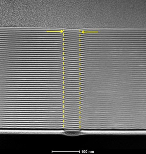
7 Absorber patterning Absorber patterning at Samsung mask Shop Patterning with high-end EBW tool and EUV mask etcher Modified etch chemistry due to 1.5 times slower ER than commercial absorber Acquired excellent pattern quality and critical dimension SEM AFM 88degs 2.8nm LWR MTT:1.9nm 88nm 108nm 128nm 7


8 Simulation Exposure Absorber ML geometry Simulation CD Analysis Smoothed D P S Conventional Ill. NA:0.25, σ:0.8 Position: X=0 Conformal R C W A (CD 1 CD 2 )x100 CD error = CD 1 Reconstructed Defect : 24/30/36/42/48nm on substrate Absorber pattern : 27nm with 88degs of SWA 8
9 ML Geometry ML growth is dependent on the process and configuration of H/W of ML deposition. Defect shape changes the ML geometry No universal ML growth model could give versatility in defect printability simulation It is very important to select the optimum ML geometry to increase simulation accuracy Used the AFM data measured from substrate and surface of ML to make a new ML geometry. 9
 Smoothed ML Geometry")

10 Smoothed Geometry (for 35nm defect) Smoothed ML Geometry 35nm ML pairs Defect dimension Good for any type of defect? 10


11 Conformal Geometry Conformal ML Geometry 75nm Which model should we use for simulation? Need to find out the optimum ML geometry for each defect 11


12 Normalized Dimension Surface β Substrate α Normalized dimension : Surf. dimension β / Sub. dimension α Measured and got the all normalized dimension from 24nm, 30nm, 36nm, 42nm and 48nm defects 12


13 Fitting ML geometry 13

14 Reconstructed ML geometry Defined each defect s dimension based on the fitting curve. Created Reconstructed ML geometry Compared the CD error simulated by three types of ML geometry. (Conformal vs Smoothed vs Reconstructed ML) 14
 Illumination Defocus NA=0.25, sigma=0.8 Focus = 0nm Simul.")
15 CD error with defect dimension EUV Mask Geometry Cutline Bump Through Center of Defect Position : X= X Mask Distance (nm) Illumination Defocus NA=0.25, sigma=0.8 Focus = 0nm Simul. image Wafer image 15
 Illumination Defocus NA=0.25, sigma=0.8 Focus = 0nm Simul. image Wafer image 16")
16 CD error with defect dimension Pit EUV Mask Geometry Cutline Through Center of Defect Position : X= X Mask Distance (nm) Illumination Defocus NA=0.25, sigma=0.8 Focus = 0nm Simul. image Wafer image 16
 Illumination Defect dim. NA=0.25, sigma=0.8 24nm Simul.")
17 CD error with defocus EUV Mask Geometry Cutline Bump Through Center of Defect Position : X= X Mask Distance (nm) Illumination Defect dim. NA=0.25, sigma=0.8 24nm Simul. image Wafer image
18 CD error with defocus Pit EUV Mask Geometry Cutline Through Center of Defect Position : X= X Mask Distance (nm) Illumination Defect dim. NA=0.25, sigma=0.8 24nm Simul. image Wafer image
19 DPS performance CD error from DPS, RCWA and wafer are within 2% range DPS S/W developed by Luminescent Technologies shows good simulation accuracy while taking less calculation time than that of RCWA simulation.
20 Summary Analyzed defect dimensions measured on the substrate and the ML surface and found correlation between defect dimension and ML geometry The reconstructed ML geometry predicts the CD error better than conventional conformal ML geometry. 24nm bump and pit defects on substrate occurs 7.6% and 17% of wafer CD error showing that the Teron can detect the most of defects which could be printed on wafer for 27nmHP node L&S pattern. DPS shows good accuracy and faster calculation time than RCWA simulator.
21 Acknowledgements. Dr. Tsukasa Abe and Naoya Hayashi, DNP for discussing mask manufacturing. Dr. Eric Gullikson from LBNL for providing metrology to measure the optical properties of SEMATECH s absorber. Gregg Inderhees from KLA-Tencor for providing blank inspection. Dr. Tae-Geun Kim and Dr. Sang-Hyun Kim from Samsung for supporting the defect analysis for this study.
Lithography Industry Collaborations
 Accelerating the next technology revolution Lithography Industry Collaborations SOKUDO Breakfast July 13, 2011 Stefan Wurm SEMATECH Copyright 2009 SEMATECH, Inc. SEMATECH, and the SEMATECH logo are registered
2009 International Workshop on EUV Lithography
 Contents Introduction Absorber Stack Optimization Non-flatness Correction Blank Defect and Its Mitigation Wafer Printing Inspection Actinic Metrology Cleaning and Repair Status Remaining Issues in EUV
State of the art EUV mask blank inspection with a Lasertec M7360 at the SEMATECH MBDC
 State of the art EUV mask blank inspection with a Lasertec M7360 at the SEMATECH MBDC Patrick Kearney a, Won-Il Cho a, Chan-Uk Jeon a, Eric Gullikson b, Anwei Jia c, Tomoya Tamura c, Atsushi Tajima c,
EUV Interference Lithography in NewSUBARU
 EUV Interference Lithography in NewSUBARU Takeo Watanabe 1, Tae Geun Kim 2, Yasuyuki Fukushima 1, Noki Sakagami 1, Teruhiko Kimura 1, Yoshito Kamaji 1, Takafumi Iguchi 1, Yuuya Yamaguchi 1, Masaki Tada
Challenges of EUV masks and preliminary evaluation
 Challenges of EUV masks and preliminary evaluation Naoya Hayashi Electronic Device Laboratory Dai Nippon Printing Co.,Ltd. EUV Mask Workshop 2004 1 Contents Recent Lithography Options on Roadmap Challenges
Comparison of actinic and non-actinic inspection of programmed defect masks
 Comparison of actinic and non-actinic inspection of programmed defect masks Funded by Kenneth Goldberg, Anton Barty Hakseung Han*, Stefan Wurm*, Patrick Kearney, Phil Seidel Obert Wood*, Bruno LaFontaine
EUV Substrate, Blank, and Mask Flatness Current Specifications & Issues Overview
 EUV Mask Flatness & Carrier/Loadport Workshop October 19 th 2006 - Barcelona Spain EUV Substrate, Blank, and Mask Flatness Current Specifications & Issues Overview Phil Seidel, Chris Van Peski Stefan Wurm
Progresses in NIL Template Fabrication Naoya Hayashi
 Progresses in NIL Template Fabrication Naoya Hayashi Electronic Device Operations Dai Nippon Printing Co., Ltd. Contents 1. Introduction Motivation NIL mask fabrication process 2. NIL mask resolution improvement
Light Sources for EUV Mask Metrology. Heiko Feldmann, Ulrich Müller
 Light Sources for EUV Mask Metrology Heiko Feldmann, Ulrich Müller Dublin, October 9, 2012 Agenda 1 2 3 4 Actinic Metrology in Mask Making The AIMS EUV Concept Metrology Performance Drivers and their Relation
Computational Lithography Requirements & Challenges for Mask Making. Naoya Hayashi, Dai Nippon Printing Co., Ltd
 Computational Lithography Requirements & Challenges for Mask Making Naoya Hayashi, Dai Nippon Printing Co., Ltd Contents Introduction Lithography Trends Computational lithography options More Complex OPC
Defect printability of thin absorber mask in EUV lithography with refined LER resist
 [#5, MA] Defect printability of thin absorber mask in EUV lithography with refined LER resist Takashi Kamo, Hajime Aoyama, Yukiyasu Arisawa, Mihoko Kijima, Toshihiko Tanaka and Osamu Suga e-mail: kamo.takashi@selete.co.jp
Progress in full field EUV lithography program at IMEC
 Progress in full field EUV lithography program at IMEC A.M. Goethals*, G.F. Lorusso*, R. Jonckheere*, B. Baudemprez*, J. Hermans*, F. Iwamoto 1, B.S. Kim 2, I.S. Kim 2, A. Myers 3, A. Niroomand 4, N. Stepanenko
Mask Technology Development in Extreme-Ultraviolet Lithography
 Mask Technology Development in Extreme-Ultraviolet Lithography Anthony Yen September 6, 2013 Projected End of Optical Lithography 2013 TSMC, Ltd 1976 1979 1982 1985 1988 1991 1994 1997 2000 2003 2007 2012
Characterization of Actinic Mask Blank Inspection for Improving Sensitivity
 Characterization of Actinic Mask Blank Inspection for Improving Sensitivity Yoshihiro Tezuka, Toshihiko Tanaka, Tsuneo Terasawa, Toshihisa Tomie * M-ASET, Tsukuba, Japan * M-ASRC, AIST, Tsukuba, Japan
Recent Development Activities on EUVL at ASET
 Title Recent Development Activities on at ASET Shinji Okazaki ASET Laboratory 2 nd International Workshop on 1 Overall Development Plan 98 99 00 01 02 03 04 05 06 07 08 ASET Basic Technologies 100% Government
Development of ultra-fine structure t metrology system using coherent EUV source
 2009 International Workshop On EUV Lithography, July 13-17,2009 Development of ultra-fine structure t metrology system using coherent EUV source University of Hyogo 1, Hiroo Kinoshita 1,3, Tetuo Harada
Recent Activities of the Actinic Mask Inspection using the EUV microscope at Center for EUVL
 Recent Activities of the Actinic Mask Inspection using the EUV microscope at Center for EUVL Takeo Watanabe, Tetsuo Harada, and Hiroo Kinoshita Center for EUVL, University of Hyogo Outline 1) EUV actinic
Evaluation of Technology Options by Lithography Simulation
 Evaluation of Technology Options by Lithography Simulation Andreas Erdmann Fraunhofer IISB, Erlangen, Germany Semicon Europe, Dresden, October 12, 2011 Outline Introduction: Resolution limits of optical
Impact of 3-D Mask Effects on CD and Overlay over Image Field in Extreme Ultraviolet Lithography
 Impact of 3-D Mask Effects on CD and Overlay over Image Field in Extreme Ultraviolet Lithography 5 th International EUV Symposium Barcelona, Spain Sven Trogisch Markus Bender Frank-Michael Kamm Disclaimer
Eun-Jin Kim, GukJin Kim, Seong-Sue Kim*, Han-Ku Cho*, Jinho Ahn**, Ilsin An, and Hye-Keun Oh
 Eun-Jin Kim, GukJin Kim, Seong-Sue Kim*, Han-Ku Cho*, Jinho Ahn**, Ilsin An, and Hye-Keun Oh Lithography Lab. Department of Applied Physics, Hanyang University, Korea *Samsung Electronics Co., LTD. Korea
R&D Status and Key Technical and Implementation Challenges for EUV HVM
 R&D Status and Key Technical and Implementation Challenges for EUV HVM Sam Intel Corporation Agenda Requirements by Process Node EUV Technology Status and Gaps Photoresists Tools Reticles Summary 2 Moore
TSMC Property. EUV Lithography. The March toward HVM. Anthony Yen. 9 September TSMC, Ltd
 EUV Lithography The March toward HVM Anthony Yen 9 September 2016 1 1 st EUV lithography setup and results, 1986 Si Stencil Mask SR W/C Multilayer Coating Optics λ=11 nm, provided by synchrotron radiation
EUV Multilayer Fabrication
 EUV Multilayer Fabrication Rigaku Innovative Technologies Inc. Yuriy Platonov, Michael Kriese, Jim Rodriguez ABSTRACT: In this poster, we review our use of tools & methods such as deposition flux simulation
Critical Challenges of EUV Mask Blank Volume Production
 Critical Challenges of EUV Mask Blank Volume Production Holger Seitz, Markus Renno, Thomas Leutbecher, Nathalie Olschewski, Helmut Popp, Torsten Reichardt, Ronny Walter, Günter Hess SCHOTT Lithotec AG,
Shot noise and process window study for printing small contacts using EUVL. Sang Hun Lee John Bjorkohlm Robert Bristol
 Shot noise and process window study for printing small contacts using EUVL Sang Hun Lee John Bjorkohlm Robert Bristol Abstract There are two issues in printing small contacts with EUV lithography (EUVL).
IMEC update. A.M. Goethals. IMEC, Leuven, Belgium
 IMEC update A.M. Goethals IMEC, Leuven, Belgium Outline IMEC litho program overview ASML ADT status 1 st imaging Tool description Resist projects Screening using interference litho K LUP / Novel resist
EUV Micro-Exposure Tool (MET) for Near-Term Development Using a High NA Projection System
 for Near-Term Development Using a High NA Projection System") EUV Micro-Exposure Tool (MET) for Near-Term Development Using a High NA Projection System John S. Taylor, Donald Sweeney, Russell Hudyma Layton Hale, Todd Decker Lawrence Livermore National Laboratory
EUV Micro-Exposure Tool (MET) for Near-Term Development Using a High NA Projection System John S. Taylor, Donald Sweeney, Russell Hudyma Layton Hale, Todd Decker Lawrence Livermore National Laboratory
Lithography Roadmap. without immersion lithography. Node Half pitch. 248nm. 193nm. 157nm EUVL. 3-year cycle: 2-year cycle: imec 2005
 Lithography Roadmap without immersion lithography Node Half pitch 180 nm 130 nm 90 nm 65 nm 45 nm 32 nm 22 nm 250 nm 180 nm 130 nm 90 nm 65 nm 45 nm 32 nm 248nm 193nm 157nm EUVL 3-year cycle: 2-year cycle:
The End of Thresholds: Subwavelength Optical Linewidth Measurement Using the Flux-Area Technique
 The End of Thresholds: Subwavelength Optical Linewidth Measurement Using the Flux-Area Technique Peter Fiekowsky Automated Visual Inspection, Los Altos, California ABSTRACT The patented Flux-Area technique
EUVL: Challenges to Manufacturing Insertion
 EUVL: Challenges to Manufacturing Insertion Obert R Wood II International Workshop on EUV Lithography CXRO, LBNL, Berkeley, California 14 June 2017 EUV Critical Issues List EUV Critical Issues, as identified
ISMI 450mm Transition Program
 SEMATECH Symposium Japan September 15, 2010 Accelerating Manufacturing Productivity ISMI 450mm Transition Program Scott Kramer VP Manufacturing Technology SEMATECH Copyright 2010 SEMATECH, Inc. SEMATECH,
Electron Multi-Beam Technology for Mask and Wafer Direct Write. Elmar Platzgummer IMS Nanofabrication AG
 Electron Multi-Beam Technology for Mask and Wafer Direct Write Elmar Platzgummer IMS Nanofabrication AG Contents 2 Motivation for Multi-Beam Mask Writer (MBMW) MBMW Tool Principles and Architecture MBMW
Diffractive optical elements and their potential role in high efficiency illuminators
 Diffractive optical elements and their potential role in high efficiency illuminators Patrick Naulleau Farhad Salmassi, Eric Gullikson, Erik Anderson Lawrence Berkeley National Laboratory Patrick Naulleau
Actinic Review of EUV Masks: Status and Recent Results of the AIMS TM EUV System
 Actinic Review of EUV Masks: Status and Recent Results of the AIMS TM EUV System Sascha Perlitz a, Jan Hendrik Peters a, Markus Weiss b, Dirk Hellweg b, Renzo Capelli b, Krister Magnusson b, Matt Malloy
Jung Sik Kim, Seongchul Hong, Jae Uk Lee, Seung Min Lee, and Jinho Ahn*
 Jung Sik Kim, Seongchul Hong, Jae Uk Lee, Seung Min Lee, and Jinho Ahn* Photon shot noise effect in EUVL Degrades stochastic imaging performance Suggestion of a thin attenuated PSM Comparing PSM with conventional
Progress towards Actinic Patterned Mask Inspection. Oleg Khodykin
 Progress towards Actinic Patterned Mask Inspection Oleg Khodykin Outline Status (technical) of EUV Actinic Reticle Inspection program Xe based LPP source as bright and reliable solution Requirements Choice
2008 European EUVL. EUV activities the EUVL shop future plans. Rob Hartman
 2008 European EUVL EUV activities the EUVL shop future plans Rob Hartman 2007 international EUVL Symposium 28-31 October 2007 2008 international EUVL Symposium 28 Sapporo, September Japan 1 October 2008
EUVL getting ready for volume introduction
 EUVL getting ready for volume introduction SEMICON West 2010 Hans Meiling, July 14, 2010 Slide 1 public Outline ASML s Lithography roadmap to support Moore s Law Progress on 0.25NA EUV systems Progress
ISMI 450mm Transition Program
 SEMATECH Symposium Taiwan September 7, 2010 Accelerating Manufacturing Productivity ISMI 450mm Transition Program Scott Kramer VP Manufacturing Technology SEMATECH Copyright 2010 SEMATECH, Inc. SEMATECH,
Key Challenges in EUV Mask Technology: Actinic Mask Inspection and Mask 3D Effects. Yow-Gwo Wang
 Key Challenges in EUV Mask Technology: Actinic Mask Inspection and Mask 3D Effects by Yow-Gwo Wang A dissertation submitted in partial satisfaction of the requirements for the degree of Doctor of Philosophy
Using the Normalized Image Log-Slope, part 2
 T h e L i t h o g r a p h y E x p e r t (Spring ) Using the Normalized Image Log-Slope, part Chris A. Mack, FINLE Technologies, A Division of KLA-Tencor, Austin, Texas As we saw in part of this column,
Holistic Lithography. Christophe Fouquet. Executive Vice President, Applications. 24 November 2014
 Holistic Lithography Christophe Fouquet Executive Vice President, Applications 24 Holistic Lithography Introduction Customer Problem: Beyond 20nm node scanner and non scanner contributions must be addressed
Actinic Review of EUV Masks: Performance Data and Status of the AIMS TM EUV System
 Actinic Review of EUV Masks: Performance Data and Status of the AIMS TM EUV System Dirk Hellweg*, Markus Koch, Sascha Perlitz, Martin Dietzel, Renzo Capelli Carl Zeiss SMT GmbH, Rudolf-Eber-Str. 2, 73447
ISMI Industry Productivity Driver
 SEMATECH Symposium Japan September 15, 2010 Accelerating Manufacturing Productivity ISMI Industry Productivity Driver Scott Kramer VP Manufacturing Technology SEMATECH Copyright 2010 SEMATECH, Inc. SEMATECH,
UV Nanoimprint Stepper Technology: Status and Roadmap. S.V. Sreenivasan Sematech Litho Forum May 14 th, 2008
 UV Nanoimprint Stepper Technology: Status and Roadmap S.V. Sreenivasan Sematech Litho Forum May 14 th, 2008 Overview Introduction Stepper technology status: Patterning and CD Control Through Etch Alignment
Lithography Simulation Tools Needed for 22nm HP and Beyond. Chris Mack
 Lithography Simulation Tools Needed for 22nm HP and Beyond Chris Mack www.lithoguru.com Slicing the Pie Simulation Tool Characteristics Precision Accuracy Capabilities (speed, features) Simulation Tool
Towards an affordable Cost of Ownership for EUVL. Melissa Shell Principal Engineer & Program Manager, EUVL Research Components Research October 2006
 Towards an affordable Cost of Ownership for EUVL Melissa Shell Principal Engineer & Program Manager, EUVL Research Components Research October 2006 1 Robert Bristol Heidi Cao Manish Chandhok Michael Leeson
EUVL Activities in China. Xiangzhao Wang Shanghai Inst. Of Opt. and Fine Mech. Of CAS. (SIOM) Shanghai, China.
 Shanghai, China.") EUVL Activities in China Xiangzhao Wang Shanghai Inst. Of Opt. and Fine Mech. Of CAS. (SIOM) Shanghai, China. wxz26267@siom.ac.cn Projection Optics Imaging System Surface Testing Optical Machining ML Coating
EUVL Activities in China Xiangzhao Wang Shanghai Inst. Of Opt. and Fine Mech. Of CAS. (SIOM) Shanghai, China. wxz26267@siom.ac.cn Projection Optics Imaging System Surface Testing Optical Machining ML Coating
EUV Actinic Blank Inspection Tool Development
 EUV Actinic Blank Inspection Tool Development EUVL Symposium 2011 Hiroki Miyai 1, Tomohiro Suzuki 1, Kiwamu Takehisa 1, Haruhiko Kusunose 1, Takeshi Yamane 2, Tsuneo Terasawa 2, Hidehiro Watanabe 2, Soichi
Optolith 2D Lithography Simulator
 2D Lithography Simulator Advanced 2D Optical Lithography Simulator 4/13/05 Introduction is a powerful non-planar 2D lithography simulator that models all aspects of modern deep sub-micron lithography It
OPC Rectification of Random Space Patterns in 193nm Lithography
 OPC Rectification of Random Space Patterns in 193nm Lithography Mosong Cheng, Andrew Neureuther, Keeho Kim*, Mark Ma*, Won Kim*, Maureen Hanratty* Department of Electrical Engineering and Computer Sciences
Advanced Patterning Techniques for 22nm HP and beyond
 Advanced Patterning Techniques for 22nm HP and beyond An Overview IEEE LEOS (Bay Area) Yashesh A. Shroff Intel Corporation Aug 4 th, 2009 Outline The Challenge Advanced (optical) lithography overview Flavors
EUV Lithography Transition from Research to Commercialization
 EUV Lithography Transition from Research to Commercialization Charles W. Gwyn and Peter J. Silverman and Intel Corporation Photomask Japan 2003 Pacifico Yokohama, Kanagawa, Japan Gwyn:PMJ:4/17/03:1 EUV
EUV Substrate and Blank Inspection
 EUV Substrate and Blank Inspection SEMATECH EUV Workshop 10/11/99 Steve Biellak KLA-Tencor RAPID Division *This work is partially funded by NIST-ATP project 98-06, Project Manager Purabi Mazumdar 1 EUV
Comparative Study of Binary Intensity Mask and Attenuated Phase Shift Mask using Hyper-NA Immersion Lithography for Sub-45nm Era
 Comparative Study of Binary Intensity Mask and Attenuated Phase Shift Mask using Hyper-NA Immersion Lithogr for Sub-45nm Era Tae-Seung Eom*, Jun-Taek Park, Sarohan Park, Sunyoung Koo, Jin-Soo Kim, Byoung-Hoon
MASK 3D EFFECTS FIRST EXPERIMENTAL MEASUREMENTS WITH NA 0.55 ANAMORPHIC IMAGING
 MASK 3D EFFECTS FIRST EXPERIMENTAL MEASUREMENTS WITH NA 0.55 ANAMORPHIC IMAGING VINCENT WIAUX, VICKY PHILIPSEN, ERIC HENDRICKX EUVL WORKSHOP. BERKELEY, JUNE 13 th, 2018. PUBLIC EUV MASK 3D EFFECTS EXPERIMENTAL
The future of EUVL. Outline. by Winfried Kaiser, Udo Dinger, Peter Kuerz, Martin Lowisch, Hans-Juergen Mann, Stefan Muellender,
 The future of EUVL by Winfried Kaiser, Udo Dinger, Peter Kuerz, Martin Lowisch, Hans-Juergen Mann, Stefan Muellender, William H. Arnold, Jos Benshop, Steven G. Hansen, Koen van Ingen-Schenau Outline Introduction
Lithography on the Edge
 Lithography on the Edge David Medeiros IBM Prague, Czech Republic 3 October 009 An Edge A line where an something begins or ends: A border, a discontinuity, a threshold Scaling Trend End of an Era? 0000
A Study of Wafer Plane Analysis with Mask MVM-SEM using 2D and 3D Images
 A Study of Wafer Plane Analysis with Mask MVM-SEM using 2D and 3D Images Takayuki Nakamura ADVANTEST CORPORATION February 24, 2015 San Jose, California Member 2015/2/20 All Rights Reserved - ADVANTEST
TECHNOLOGY ROADMAP 2011 EDITION LITHOGRAPHY FOR
 INTERNATIONAL TECHNOLOGY ROADMAP FOR SEMICONDUCTORS 2011 EDITION LITHOGRAPHY THE ITRS IS DEVISED AND INTENDED FOR TECHNOLOGY ASSESSMENT ONLY AND IS WITHOUT REGARD TO ANY COMMERCIAL CONSIDERATIONS PERTAINING
Copyright 2000 by the Society of Photo-Optical Instrumentation Engineers.
 Copyright 2000 by the Society of Photo-Optical Instrumentation Engineers. This paper was published in the proceedings of the 20 th Annual BACUS Symposium on Photomask Technology SPIE Vol. 4186, pp. 503-507.
Novel EUV Resist Development for Sub-14nm Half Pitch
 EUV Workshop 2015 Maui, HI P64 Novel EUV Resist Development for Sub-14nm Half Pitch Yoshi Hishiro JSR Micro Inc. EUV Workshop, June 17, 2015 1 Contents Requirement for sub-14nm HP EUV resist JSR strategy
Decomposition difficulty analysis for double patterning and. the impact on photomask manufacturability
 Decomposition difficulty analysis for double patterning and the impact on photomask manufacturability Yuichi Inazuki 1*, Nobuhito Toyama, Takaharu Nagai 1, Takanori Sutou 1, Yasutaka Morikawa 1, Hiroshi
Shooting for the 22nm Lithography Goal with the. Coat/Develop Track. SOKUDO Lithography Breakfast Forum 2010 July 14 (L1)
") Shooting for the 22nm Lithography Goal with the Coat/Develop Track SOKUDO Lithography Breakfast Forum 2010 July 14 (L1) Three (3) different exposure options for 22nm: Public External (L1) MAPPER Lithography
Shooting for the 22nm Lithography Goal with the Coat/Develop Track SOKUDO Lithography Breakfast Forum 2010 July 14 (L1) Three (3) different exposure options for 22nm: Public External (L1) MAPPER Lithography
450mm silicon wafers specification challenges. Mike Goldstein Intel Corp.
 450mm silicon wafers specification challenges Mike Goldstein Intel Corp. Outline Background 450mm transition program 450mm silicon evolution Mechanical grade wafers (spec case study) Developmental (test)
Scaling of Semiconductor Integrated Circuits and EUV Lithography
 Scaling of Semiconductor Integrated Circuits and EUV Lithography ( 半導体集積回路の微細化と EUV リソグラフィー ) December 13, 2016 EIDEC (Emerging nano process Infrastructure Development Center, Inc.) Hidemi Ishiuchi 1 OUTLINE
Line Width Roughness Control for EUV Patterning
 Line Width Roughness Control for EUV Patterning Shinichiro Kawakami, Lior Huli, Shannon Dunn, Akiteru Ko TEL Technology Center, America, LLC., 255 Fuller Road, STE 244, Albany, NY 12203 USA Karen Petrillo,
The SEMATECH Model: Potential Applications to PV
 Continually cited as the model for a successful industry/government consortium Accelerating the next technology revolution The SEMATECH Model: Potential Applications to PV Dr. Michael R. Polcari President
IMPACT Lithography/DfM Roundtable
 IMPACT Lithography/DfM Roundtable Focus Match Location Z 0 Neureuther Research Group Juliet Rubinstein, Eric Chin, Chris Clifford, Marshal Miller, Lynn Wang, Kenji Yamazoe Visiting Industrial Fellow, Canon,
Feature-level Compensation & Control
 Feature-level Compensation & Control 2 Lithography Andrew Neureuther and Costas Spanos, UCB Workshop & Review 04/15/2004 11/19/2003 - Lithography 3 Lithography: Andy Neureuther, UCB Research Themes: Linking
EUVL Challenges for Next Generation Devices
 EUVL Challenges for Next Generation Devices Center for Semiconductor Research & Development Advanced Lithography Process Technology Dept. Tatsuhiko Higashiki Contents Device Roadmap and Lithography Extendibility
TECHNOLOGY ROADMAP 2006 UPDATE LITHOGRAPHY FOR
 INTERNATIONAL TECHNOLOGY ROADMAP FOR SEMICONDUCTORS 2006 UPDATE LITHOGRAPHY THE ITRS IS DEVISED AND INTENDED FOR TECHNOLOGY ASSESSMENT ONLY AND IS WITHOUT REGARD TO ANY COMMERCIAL CONSIDERATIONS PERTAINING
Copyright 2000, Society of Photo-Optical Instrumentation Engineers This paper was published in Optical Microlithography XIII, Volume 4000 and is made
 Copyright 00, Society of Photo-Optical Instrumentation Engineers This paper was published in Optical Microlithography XIII, Volume 4000 and is made available as an electronic reprint with permission of
INTERNATIONAL TECHNOLOGY ROADMAP SEMICONDUCTORS 2001 EDITION LITHOGRAPHY FOR
 INTERNATIONAL TECHNOLOGY ROADMAP FOR SEMICONDUCTORS 2001 EDITION LITHOGRAPHY TABLE OF CONTENTS Scope...1 Difficult Challenges...1 Lithography Technology Requirements...3 Potential Solutions...14 Crosscut
Optical Lithography. Keeho Kim Nano Team / R&D DongbuAnam Semi
 Optical Lithography Keeho Kim Nano Team / R&D DongbuAnam Semi Contents Lithography = Photolithography = Optical Lithography CD : Critical Dimension Resist Pattern after Development Exposure Contents Optical
immersion optics Immersion Lithography with ASML HydroLith TWINSCAN System Modifications for Immersion Lithography by Bob Streefkerk
 immersion optics Immersion Lithography with ASML HydroLith by Bob Streefkerk For more than 25 years, many in the semiconductor industry have predicted the end of optical lithography. Recent developments,
High-NA EUV lithography enabling Moore s law in the next decade
 High-NA EUV lithography enabling Moore s law in the next decade Jan van Schoot, Kars Troost, Alberto Pirati, Rob van Ballegoij, Peter Krabbendam, Judon Stoeldraijer, Erik Loopstra, Jos Benschop, Jo Finders,
Closed Loop Registration Control (RegC ) Using PROVE as the Data Source for the RegC Process
 Using PROVE as the Data Source for the RegC Process") Invited Paper Closed Loop Registration Control (RegC ) Using PROVE as the Data Source for the RegC Process Erez Graitzer 1 ; Avi Cohen 1 ; Vladimir Dmitriev 1 ; Itamar Balla 1 ; Dan Avizemer 1 Dirk Beyer
Invited Paper Closed Loop Registration Control (RegC ) Using PROVE as the Data Source for the RegC Process Erez Graitzer 1 ; Avi Cohen 1 ; Vladimir Dmitriev 1 ; Itamar Balla 1 ; Dan Avizemer 1 Dirk Beyer
Double Patterning Combined with Shrink Technique to Extend ArF Lithography for Contact Holes to 22nm Node and Beyond
 Double Patterning Combined with Shrink Technique to Extend ArF Lithography for Contact Holes to 22nm Node and Beyond Xiangqun Miao* a, Lior Huli b, Hao Chen a, Xumou Xu a, Hyungje Woo a, Chris Bencher
In-line focus monitoring and fast determination of best focus using scatterometry
 In-line focus monitoring and fast determination of best focus using scatterometry a Steven Thanh Ha, a Benjamin Eynon, a Melany Wynia, a Jeff Schmidt, b Christian Sparka, b Antonio Mani, b Roie Volkovich,
Process Optimization
 Process Optimization Process Flow for non-critical layer optimization START Find the swing curve for the desired resist thickness. Determine the resist thickness (spin speed) from the swing curve and find
EUVL: Challenges to Manufacturing Insertion
 Journal of Photopolymer Science and Technology Volume 30, Number 5 (2017) 599-604 C 2017SPST Technical Paper EUVL: Challenges to Manufacturing Insertion Obert R. Wood II * Strategic Lithography Technology,
Multi-Beam activity from the 1980s. Apr 18, 2013 Panel Discussion Photomask Japan 2013
 Multi-Beam activity from the 1980s 1 Panel Discussion Multi-Beam Mask Writer Hans Loeschner IMS Nanofabrication AG Vienna, Austria Jiun Sonja (1718-1805) Buji Kore Kinin Only those who live simply, live
Discovering Electrical & Computer Engineering. Carmen S. Menoni Professor Week 3 armain.
 Discovering Electrical & Computer Engineering Carmen S. Menoni Professor Week 3 http://www.engr.colostate.edu/ece103/semin armain.html TOP TECH 2012 SPECIAL REPORT IEEE SPECTRUM PAGE 28, JANUARY 2012 P.E.
Collector development with IR suppression and EUVL optics refurbishment at RIT
 Collector development with IR suppression and EUVL optics refurbishment at RIT Yuriy Platonov, Michael Kriese, Raymond Crucet, Yang Li, Vladimir Martynov, Licai Jiang, Jim Rodriguez Rigaku Innovative Technologies
A process for, and optical performance of, a low cost Wire Grid Polarizer
 1.0 Introduction A process for, and optical performance of, a low cost Wire Grid Polarizer M.P.C.Watts, M. Little, E. Egan, A. Hochbaum, Chad Jones, S. Stephansen Agoura Technology Low angle shadowed deposition
Holistic View of Lithography for Double Patterning. Skip Miller ASML
 Holistic View of Lithography for Double Patterning Skip Miller ASML Outline Lithography Requirements ASML Holistic Lithography Solutions Conclusions Slide 2 Shrink Continues Lithography keeps adding value
III-V on Si for VLSI. 200 mm III-V on Si. Accelerating the next technology revolution. III-V nfet on 200 mm Si
 III-V on Si for VLSI Accelerating the next technology revolution 200 mm III-V on Si III-V nfet on 200 mm Si R. Hill, C. Park, J. Barnett, J. Huang, N. Goel, J. Oh, W.Y. Loh, J. Price, P. Kirsch, P, Majhi,
EUV Resists: Pushing to the Extreme
 Journal of Photopolymer Science and Technology Volume 27, Number 6 (2014) 725 730 2014SPST Technical Paper EUV Resists: Pushing to the Extreme Patrick Naulleau 1, Christopher Anderson 1, Weilun Chao 1,
Overlay accuracy a metal layer study
 Overlay accuracy a metal layer study Andrew Habermas 1, Brad Ferguson 1, Joel Seligson 2, Elyakim Kassel 2, Pavel Izikson 2 1 Cypress Semiconductor, 2401 East 86 th St, Bloomington, MN 55425, USA 2 KLA-Tencor,
Etch, Deposition, and Metrology Options for Cost-Effective Thin-Film Bulk Acoustic Resonator (FBAR) Production
 Production") Etch, Deposition, and Metrology Options for Cost-Effective Thin-Film Bulk Acoustic Resonator (FBAR) Production Figure 1 Veeco is driving System on a Chip Technology Frank M. Cumbo, Kurt E. Williams, John
Etch, Deposition, and Metrology Options for Cost-Effective Thin-Film Bulk Acoustic Resonator (FBAR) Production Figure 1 Veeco is driving System on a Chip Technology Frank M. Cumbo, Kurt E. Williams, John
The Coherent EUV Scatterometry Microscope for Actinic Mask Inspection and Metrology
 The Coherent EUV Scatterometry Microscope for Actinic Mask Inspection and Metrology Tetsuo Harada* 1,3, Masato Nakasuji 1,3, Teruhiko Kimura 1,3, Yutaka Nagata 2,3, Takeo Watanabe 1,3, Hiroo Kinoshita
Double Patterning Combined with Shrink Technique to Extend ArF Lithography for Contact Holes to 22nm Node and Beyond
 Double Patterning Combined with Shrink Technique to Extend ArF Lithography for Contact Holes to 22nm Node and Beyond Juliet Xiangqun Miao, Lior Huli b, Hao Chen, Xumou Xu, Hyungje Woo, Chris Bencher, Jen
Resist Process Window Characterization for the 45-nm Node Using an Interferometric Immersion microstepper
 Rochester Institute of Technology RIT Scholar Works Presentations and other scholarship 3-29-2006 Resist Process Window Characterization for the 45-nm Node Using an Interferometric Immersion microstepper
16nm with 193nm Immersion Lithography and Double Exposure
 16nm with 193nm Immersion Lithography and Double Exposure Valery Axelrad, Sequoia Design Systems, Inc. (United States) Michael C. Smayling, Tela Innovations, Inc. (United States) ABSTRACT Gridded Design
Tutor43.doc; Version 8/15/03 T h e L i t h o g r a p h y E x p e r t (November 2003)
") Tutor43.doc; Version /15/03 T h e L i t h o g r a p h y E x p e r t (November 2003) Scattering Bars Chris A. Mack, KLA-Tencor, FINLE Division, Austin, Texas Resolution enhancement technologies refer to
Tutor43.doc; Version /15/03 T h e L i t h o g r a p h y E x p e r t (November 2003) Scattering Bars Chris A. Mack, KLA-Tencor, FINLE Division, Austin, Texas Resolution enhancement technologies refer to
A New Inspection Method for a EUV Mask Defect Inspection System
 A New Inspection Method for a EUV Mask Defect Inspection System Ding Qi 1, Kuen-Yu Tsai* 1, Jia-Han Li 2 1 Department of Electrical Engineering 2 Department of Engineering Science and Ocean National Taiwan
Lithographic measurement of EUV flare in the 0.3-NA Micro Exposure Tool optic at the Advanced Light Source
 Lithographic measurement of EUV flare in the 0.3-NA Micro Exposure Tool optic at the Advanced Light Source Jason P. Cain, a1 Patrick Naulleau, b Costas J. Spanos a a Department of Electrical Engineering
Mask magnification at the 45-nm node and beyond
 Mask magnification at the 45-nm node and beyond Summary report from the Mask Magnification Working Group Scott Hector*, Mask Strategy Program Manager, ISMT Mask Magnification Working Group January 29,
EUV Resist Materials and Process for 16 nm Half Pitch and Beyond
 EUV Workshop 2013 June 13, 2013 EUV Resist Materials and Process for 16 nm Half Pitch and Beyond Yoshi Hishiro JSR Micro Inc. No13-2400-056 Challenge for EUV Resist & JSR approaches EUV Resist Resolution,