ISMI 450mm Transition Program
|
|
|
- Norma Hall
- 6 years ago
- Views:
Transcription


1 SEMATECH Symposium Taiwan September 7, 2010 Accelerating Manufacturing Productivity ISMI 450mm Transition Program Scott Kramer VP Manufacturing Technology SEMATECH Copyright 2010 SEMATECH, Inc. SEMATECH, and the SEMATECH logo are registered servicemarks of SEMATECH, Inc. International SEMATECH Manufacturing Initiative, ISMI, Advanced Materials Research Center and AMRC are servicemarks of SEMATECH, Inc. All other servicemarks and trademarks are the property of their respective owners.


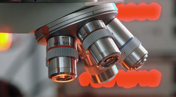
2 Wafer size the great cost equalizer 200mm 300mm 450mm ~ >2012 History shows that increasing wafer surface area by ~2.25X yields a 30% cost reduction and enables the inexpensively part of Moore s Law 2
3 ISMI 450mm program mission and organization ISMI s 450mm mission statement Enable a cost-effective 450mm transition through coordination and development of infrastructure, guidance, and industry readiness ISMI 450mm organization 450mm transition program Supplier engagement Factory integration readiness Test wafer operations Starting materials Vacuum platform development Equipment test methods and metrics 3
4 450mm progress 2007 thru 2010 Wafers Mechanical wafer bank Single crystal wafer bank test wafer generation Improved wafer quality supports equipment demonstrations Equipment Equipment concepts development Supplier engagement 1st 450mm tool (bare wafer particle detector) Equipment demonstrations Factory integration Interoperability Test Bed (ITB) prototype FI components Integrating components Full interoperability testing with standard compliant components Standards First draft ballots proposed for FOUPs and Loadports Mechanical wafer standard completed FOUP and loadport standards completed Developmental wafer standard completed
5 450mm starting materials activities 5
6 Silicon industry update All major silicon suppliers are engaged in the 450mm program and manufacturing developmental test wafers Wafer quality is continuously improving: Scratches have been eliminated Particle levels have been reduced dramatically Surface metals metrology is in development Inspection equipment is coming on line Wafer shipping methodology is in development ISMI is engaged with suppliers to close gaps in silicon manufacturing and inspection line 6


7 450mm surface quality improvements 450mm Surface Quality Improvement Wafer Defects (Lower is Better) Key Surface Parameter Target 2 0 Q3'09 Q4'09 Q1'10 Q2'10 Time Polishing has been improved scratches have been eliminated 2010 Cleaning has been improved particle levels have been reduced 10X 7
8 ISMI silicon activities Benchmark silicon suppliers state of the art Work with suppliers to improve wafer quality Continuous engagement with wafer inspection OEMs Validate wafers specification in preparation for prime wafer spec generation Wafer bank loan program has been complemented with OEMs starting to purchase wafers directly from suppliers SEMI spec M76 published for developmental 450mm polished single crystal silicon wafers We have expended our interface with materials suppliers beyond silicon (E.G. quartzware, sputtering targets), in support of ISMI process test wafers generation 8
9 ISMI test wafer operations 9
10 ISMI test wafer operations 450mm equipment installations continues Bare wafer particle/edge inspection Wafer cleaning Film thickness measurements EFEMs / wafer sorters FOUP wash 450mm test wafer processing experiments are progressing Wafer cleaning Metrology inspections ISMI continues working with suppliers on test wafer capabilities 10


11 ISMI prototype wafer cleans tool SSEC Wet clean tool installation complete in SEMATECH cleanroom SC1 / SC2 cleaning capability 12mm pitch loadport Cleaning experiments underway Cleaner wafers becoming available in ISMI wafer bank Particle experiments with loadports / carriers underway 11

12 450mm test wafer utilities matrix Collecting early 450mm utility projections Inputs will be used for 450mm test wafer facility planning Supplier surveys Consolidate surveys Supplier estimates for 450mm equipment facility requirements are requested 12
13 450mm demonstration test methodology 13
14 450 mm demonstration test methodology (450 DTM) The 450 DTM provides an efficient equipment demonstration model for the industry Consolidated inputs from IC makers and suppliers Clear and consistent procedures; standardized methodology for common equipment requirements Equipment demonstrations will focus on process repeatability, stability, and equipment reliability As demonstrations begin, engagement and input from IC maker and equipment suppliers is key 14
15 450mm factory integration 15
16 Reduced standards development time ISMI s ITB testing helped to enable a 60-65% time reduction in FI standards development vs. 300mm 300mm transition FI standards transition Org standards published Provisional or full standards published Decision to start wafer size transition and standards development Approved FI standards published 450mm transition Ongoing prototype testing


17 ITB lab testing focused on the latest FOUPs, MACs and load ports FOUPs Carriers 12mm Pitch Std FOUPs MAC Carrier 12mm Pitch Std MACs TDK 12 mm pitch load port under continuous cycling Completed >123 k cycles with FOUPs Gudeng 12mm Pitch Latch Key FOUP Brooks 12mm pitch load port, compatible with FOUPs and MACs cycling at supplier site Completed >34 k cycles with FOUPs Planning MAC testing in Q Sinfonia 12mm pitch load port cycling with latest FOUPs Completed >183 k cycles with FOUPs Working with Sinfonia to test new MAC/FOUP compatible Load port Entegris 12mm Pitch Latch Key FOUP 17

18 AMHS testing planned for H mm OHT 450mm Stocker New 450mm stockers and transport systems are under advanced development at suppliers sites ISMI will assess systems in H2 10 against ISMI 450mm guidelines and interoperability with 450mm standard carriers and load ports Goal is to demonstrate AMHS will be ready for 450mm pilot lines 18
19 Summary 450mm factory integration >5.0M robotic moves and >648k load port cycles completed in the ITB with prototype carriers Upgrades to prototype 12mm pitch Std FOUPs, load ports and EFEMs continued to demonstrate good interoperability and reliability Sun-setting ITB after completion of MAC, MAC load port (i.e., new standard load ports), and interoperability with FOUPs and MACs testing Working with AMHS Suppliers to complete evaluations of stockers and overhead hoist transport before end of
20 450mm vacuum platform development 20
21 450mm vacuum platform readiness 1st 450mm vacuum platform test is ongoing 450mm vacuum platform solutions are becoming available for EFEM and chamber integration ISMI will communicate additional guidelines to suppliers and industry organizations based on test results ISMI will continue to support the integration of process chamber and platform to enable prototype 450mm equipment development 21
22 450mm vacuum platform roadmap Phase I : Evaluation and Motivation Host ISMI 450mm workshop, with 16 suppliers Created preliminary ISMI 450mm platform guidelines Published ISMI 450mm EQP software guidelines Phase III : Evaluate the feasibility of platform standardization Project initiation Completed test plan (platform only) Engaged with 5 vacuum platform suppliers; received 1 st test proposals Completed early evaluation for 450mm platform standardization Test 1 st 450mm platform, at supplier site Encouraged suppliers to start on site test Phase II : Testing and Integration 22


23 1st 450mm platform configuration RORZE Type: Pentagon Interface # : 3 process chambers, 2 Load lock 300mm and 450mm wafer handling in the same platform 23

24 Accelerating the next technology revolution Research Development Manufacturing 24
ISMI 450mm Transition Program
 SEMATECH Symposium Japan September 15, 2010 Accelerating Manufacturing Productivity ISMI 450mm Transition Program Scott Kramer VP Manufacturing Technology SEMATECH Copyright 2010 SEMATECH, Inc. SEMATECH,
ISMI Industry Productivity Driver
 SEMATECH Symposium Japan September 15, 2010 Accelerating Manufacturing Productivity ISMI Industry Productivity Driver Scott Kramer VP Manufacturing Technology SEMATECH Copyright 2010 SEMATECH, Inc. SEMATECH,
ISMI 450 mm Industry Briefing
 Accelerating Manufacturing Productivity ISMI 450 mm Industry Briefing July 15th, 2009 SEMICON West Copyright 2009 SEMATECH, Inc. SEMATECH, and the SEMATECH logo are registered servicemarks of SEMATECH,
450mm silicon wafers specification challenges. Mike Goldstein Intel Corp.
 450mm silicon wafers specification challenges Mike Goldstein Intel Corp. Outline Background 450mm transition program 450mm silicon evolution Mechanical grade wafers (spec case study) Developmental (test)
The SEMATECH Model: Potential Applications to PV
 Continually cited as the model for a successful industry/government consortium Accelerating the next technology revolution The SEMATECH Model: Potential Applications to PV Dr. Michael R. Polcari President
G450C. Global 450mm Consortium at CNSE. Michael Liehr, General Manager G450C, Vice President for Research
 Global 450mm Consortium at CNSE Michael Liehr, General Manager G450C, Vice President for Research - CNSE Overview - G450C Vision - G450C Mission - Org Structure - Scope - Timeline The Road Ahead for Nano-Fabrication
Lithography Industry Collaborations
 Accelerating the next technology revolution Lithography Industry Collaborations SOKUDO Breakfast July 13, 2011 Stefan Wurm SEMATECH Copyright 2009 SEMATECH, Inc. SEMATECH, and the SEMATECH logo are registered
Accelerating Growth and Cost Reduction in the PV Industry
 Accelerating Growth and Cost Reduction in the PV Industry PV Technology Roadmaps and Industry Standards An Association s Approach Bettina Weiss / SEMI PV Group July 29, 2009 SEMI : The Global Association
State of the art EUV mask blank inspection with a Lasertec M7360 at the SEMATECH MBDC
 State of the art EUV mask blank inspection with a Lasertec M7360 at the SEMATECH MBDC Patrick Kearney a, Won-Il Cho a, Chan-Uk Jeon a, Eric Gullikson b, Anwei Jia c, Tomoya Tamura c, Atsushi Tajima c,
From Possible to Practical The Evolution of Nanoimprint for Patterned Media
 From Possible to Practical The Evolution of Nanoimprint for Patterned Media Paul Hofemann March 13, 2009 HDD Areal Density Industry Roadmap 10,000 Media Technology Roadmap Today Areal Density (Gbit/in
SEMATECH Defect Printability Studies
 Accelerating the next technology revolution SEMATECH Defect Printability Studies Il Yong Jang 1, Jenah Harris-Jones 1, Ranganath Teki 1, Vibhu Jindal 1, Frank Goodwin 1 Masaki Satake 2, Ying Li 2, Danping
SEMI E SPECIFICATION FOR ENHANCED CARRIER HANDOFF PARALLEL I/O INTERFACE
 SEMI E84-0301 SPECIFICATION FOR ENHANCED CARRIER HANDOFF PARALLEL I/O INTERFACE This specification was technically approved by the Global Physical Interfaces & Carriers Committee and is the direct responsibility
It s Time for 300mm Prime
 It s Time for 300mm Prime Iddo Hadar Managing Director, 300mm Prime Program Office SEMI Strategic Business Conference Napa Valley, California Tuesday, April 24, 2007 Safe Harbor Statement This presentation
Growing the Semiconductor Industry in New York: Challenges and Opportunities
 Accelerating the next technology revolution The SEMATECH New York Experience Growing the Semiconductor Industry in New York: Challenges and Opportunities Dan Armbrust President and CEO, SEMATECH April
Advancing Industry Productivity
 Advancing Industry Productivity Iddo Hadar Joint Productivity Working Group Session Austin, Texas Thursday, October 12, 2006 F O U N D A T I O N E N G I N E E R I N G G R O U P Safe Harbor Statement This
InAs Quantum-Well MOSFET for logic and microwave applications
 AWAD June 29 th 2012 Accelerating the next technology revolution InAs Quantum-Well MOSFET for logic and microwave applications T.-W. Kim, R. Hill, C. D. Young, D. Veksler, L. Morassi, S. Oktybrshky 1,
III-V on Si for VLSI. 200 mm III-V on Si. Accelerating the next technology revolution. III-V nfet on 200 mm Si
 III-V on Si for VLSI Accelerating the next technology revolution 200 mm III-V on Si III-V nfet on 200 mm Si R. Hill, C. Park, J. Barnett, J. Huang, N. Goel, J. Oh, W.Y. Loh, J. Price, P. Kirsch, P, Majhi,
26 June 2013 copyright 2013 G450C
 450 mm Equipment Demonstrations at G450C Statistics Used During Tests of the Semiconductor Industry s Latest Fab Equipment Transition Lorn Christal, G450C Program Manager Demonstration Test Execution 26
Semiconductor Technology America, Inc. COMPANY PROFILE STA. (Semiconductor Technology America, Inc.)
") COMPANY PROFILE STA () OUTLINE HISTORY 1999 Establishment 2003 Acquired ISO 9001 ; 2000 Certification 2004 Won a US$3million Export Tower Prize 2006 Won a US$5million Export Tower Prize FACILITIES Site
COMPANY PROFILE STA () OUTLINE HISTORY 1999 Establishment 2003 Acquired ISO 9001 ; 2000 Certification 2004 Won a US$3million Export Tower Prize 2006 Won a US$5million Export Tower Prize FACILITIES Site
IMI Labs Semiconductor Applications. June 20, 2016
 IMI Labs Semiconductor Applications June 20, 2016 Materials Are At the Core of Innovation in the 21st Century Weight Space Flexibility Heat Management Lightweight Energy Efficient Temperature Energy Efficient
Background: Line Item 3: Enhance the text description of the bounds of the COG volume to match the Figure 6 Modify 8.2.
 Background Statement for SEMI Draft Document #5375 Line Item Revisions to SEMI M80-1111, Mechanical Specification for Front-Opening Shipping Box Used to Transport and Ship 450 mm Wafers Notice: This background
REVISION TO SEMI M , MECHANICAL SPECIFICATION FOR FRONT-OPENING SHIPPING BOX USED TO TRANSPORT AND SHIP 300MM WAFERS
 Background Statement for SEMI Draft Document 4481B REVISION TO SEMI M31-0307, MECHANICAL SPECIFICATION FOR FRONT-OPENING SHIPPING BOX USED TO TRANSPORT AND SHIP 300MM WAFERS Note: This background statement
EUV Substrate, Blank, and Mask Flatness Current Specifications & Issues Overview
 EUV Mask Flatness & Carrier/Loadport Workshop October 19 th 2006 - Barcelona Spain EUV Substrate, Blank, and Mask Flatness Current Specifications & Issues Overview Phil Seidel, Chris Van Peski Stefan Wurm
Lithography. International SEMATECH: A Focus on the Photomask Industry
 Lithography S P E C I A L International SEMATECH: A Focus on the Photomask Industry by Wally Carpenter, International SEMATECH, Inc. (*IBM Corporation Assignee) It is well known that the semiconductor
Hard Disk Drive Industry Driving Areal Density and Lithography
 Hard Disk Drive Industry Driving Areal Density and Lithography September 18, 2008 Paul Hofemann Molecular Imprints Global Demand for Digital Storage Worldwide population penetration Internet at 20% PC
Industrial Innovation Information Days Brussels 3-4 October 2017
 Industrial Innovation Information Days Brussels 3-4 October 2017 NMBP Programme 2018 TOPICS FACTORIES OF THE FUTURE (FOF) DG RTD & DG CNECT DT-FOF-05-2019: Open Innovation for collaborative production
EUV Supporting Moore s Law
 EUV Supporting Moore s Law Marcel Kemp Director Investor Relations - Europe DB 2014 TMT Conference London September 4, 2014 Forward looking statements This document contains statements relating to certain
Plan Optik AG. Plan Optik AG PRODUCT CATALOGUE
 Plan Optik AG Plan Optik AG PRODUCT CATALOGUE 2 In order to service the high demand of wafers more quickly, Plan Optik provides off the shelf products in sizes from 2 up to 300mm diameter. Therefore Plan
Expert. Elemental Scientific VPD-ICPMS. Fully Automated Auto Scanning System ICP ICPMS AA
 Expert VPD-ICPMS Fully Automated Auto Scanning System Elemental Scientific ICP ICPMS AA Expert Features An indispensable tool for the determination of metal impurities in Si wafer Expert automates routine
MAPPER: High throughput Maskless Lithography
 MAPPER: High throughput Maskless Lithography Marco Wieland CEA- Leti Alterative Lithography workshop 1 Today s agenda Introduction Applications Qualification of on-tool metrology by in-resist metrology
Metal additive manufacturing for industrial applications. Global network of solutions centres. Applications expertise for a wide range of industries
 Brochure: Renishaw Solutions Centres for additive manufacturing Your partner for innovative manufacturing Metal additive manufacturing for industrial applications Global network of solutions centres Applications
R&D Status and Key Technical and Implementation Challenges for EUV HVM
 R&D Status and Key Technical and Implementation Challenges for EUV HVM Sam Intel Corporation Agenda Requirements by Process Node EUV Technology Status and Gaps Photoresists Tools Reticles Summary 2 Moore
Quality Assurance for the ATLAS Pixel Sensor
 Quality Assurance for the ATLAS Pixel Sensor 1st Workshop on Quality Assurance Issues in Silicon Detectors J. M. Klaiber-Lodewigs (Univ. Dortmund) for the ATLAS pixel collaboration Contents: - role of
(Complementary E-Beam Lithography)
") Extending Optical Lithography with C E B L (Complementary E-Beam Lithography) July 13, 2011 4008 Burton Drive, Santa Clara, CA 95054 Outline Complementary Lithography E-Beam Complements Optical Multibeam
Extending Optical Lithography with C E B L (Complementary E-Beam Lithography) July 13, 2011 4008 Burton Drive, Santa Clara, CA 95054 Outline Complementary Lithography E-Beam Complements Optical Multibeam
Hermetic Packaging Solutions using Borosilicate Glass Thin Films. Lithoglas Hermetic Packaging Solutions using Borosilicate Glass Thin Films
 Hermetic Packaging Solutions using Borosilicate Glass Thin Films 1 Company Profile Company founded in 2006 ISO 9001:2008 qualified since 2011 Headquarters and Production in Dresden, Germany Production
The Collaboration Engine: Enabling Innovation in Microelectronics
 The Collaboration Engine: Enabling Innovation in Microelectronics Karen Savala President, SEMI Americas Outline About SEMI Semiconductors: A History of Collaboration Collaboration in other Microelectronics
Action Line Cyber-Physical Systems Addressing the challenges and fostering innovation in Cyber-Physical Systems
 Action Line Cyber-Physical Systems Addressing the challenges and fostering innovation in Cyber-Physical Systems Dr. Holger Pfeifer Technische Universität München EIT ICT Labs Action Line Lead Cyber-Physical
Pharma Clean Assurance Programme.
 Pharma Clean Assurance Programme www.lcpackaging.com Cleaner, safer and sustainable 02 Innovative FIBC programme for premium pharma clean packaging The biggest challenge for the pharmaceutical industry
Manufacturing Case Studies: Copy Exactly (CE!) and the two-year cycle at Intel
 and the two-year cycle at Intel") Manufacturing Case Studies: Copy Exactly (CE!) and the two-year cycle at Intel Paolo A. Gargini Director Technology Strategy Intel Fellow 1 Agenda 2-year cycle Copy Exactly Conclusions 2 I see no reason
Manufacturing Case Studies: Copy Exactly (CE!) and the two-year cycle at Intel Paolo A. Gargini Director Technology Strategy Intel Fellow 1 Agenda 2-year cycle Copy Exactly Conclusions 2 I see no reason
450mm and Moore s Law Advanced Packaging Challenges and the Impact of 3D
 450mm and Moore s Law Advanced Packaging Challenges and the Impact of 3D Doug Anberg VP, Technical Marketing Ultratech SOKUDO Lithography Breakfast Forum July 10, 2013 Agenda Next Generation Technology
A Perspective on Semiconductor Equipment. R. B. Herring March 4, 2004
 A Perspective on Semiconductor Equipment R. B. Herring March 4, 2004 Outline Semiconductor Industry Overview of circuit fabrication Semiconductor Equipment Industry Some equipment business strategies Product
Technology & Manufacturing Readiness RMS
 Technology & Manufacturing Readiness Assessments @ RMS Dale Iverson April 17, 2008 Copyright 2007 Raytheon Company. All rights reserved. Customer Success Is Our Mission is a trademark of Raytheon Company.
Comparison of actinic and non-actinic inspection of programmed defect masks
 Comparison of actinic and non-actinic inspection of programmed defect masks Funded by Kenneth Goldberg, Anton Barty Hakseung Han*, Stefan Wurm*, Patrick Kearney, Phil Seidel Obert Wood*, Bruno LaFontaine
Proceedings. BiTS Shanghai October 21, Archive - Session BiTS Workshop Image: Zhu Difeng/Dollar Photo Club
 Proceedings Archive - Session 2 2015 BiTS Workshop Image: Zhu Difeng/Dollar Photo Club Proceedings With Thanks to Our Sponsors! Premier Honored Distinguished Publication Sponsor 2 Proceedings Presentation
Scaling of Semiconductor Integrated Circuits and EUV Lithography
 Scaling of Semiconductor Integrated Circuits and EUV Lithography ( 半導体集積回路の微細化と EUV リソグラフィー ) December 13, 2016 EIDEC (Emerging nano process Infrastructure Development Center, Inc.) Hidemi Ishiuchi 1 OUTLINE
ELECTRO-STATIC CHUCKS
 ELECTRO-STATIC CHUCKS REPAIR & RE-FURBISHING BY Q-FLEX INC TEL :-- 714-664-0101 E-MAIL : R.QFLEX@GMAIL.COM Q-FLEX WAS ESTABLISHED IN THE YEAR 1998 FOR MANUFACTUIIRNG FLEXIBLE AND RIGID CIRCUIT BOARDS AND
Electron Multi-Beam Technology for Mask and Wafer Direct Write. Elmar Platzgummer IMS Nanofabrication AG
 Electron Multi-Beam Technology for Mask and Wafer Direct Write Elmar Platzgummer IMS Nanofabrication AG Contents 2 Motivation for Multi-Beam Mask Writer (MBMW) MBMW Tool Principles and Architecture MBMW
Advanced Plasma Technology. High precision film thickness trimming for the TFH industry. Roth & Rau AG September 2009
 Advanced Plasma Technology High precision film thickness trimming for the TFH industry Roth & Rau AG September 2009 Product Overview IonScan Equipment for ultra-precise Surface Processing IonScan 800 Wafer
A Multi-Use Low-Cost, Integrated, Conductivity/Temperature Sensor
 A Multi-Use Low-Cost, Integrated, Conductivity/Temperature Sensor Guy J. Farruggia Areté Associates 1725 Jefferson Davis Hwy Suite 703 Arlington, VA 22202 phone: (703) 413-0290 fax: (703) 413-0295 email:
Organic Packaging Substrate Workshop Overview
 Organic Packaging Substrate Workshop Overview Organized by: International Electronics Manufacturing Initiative (inemi) Mario A. Bolanos November 17-18, 2009 1 Organic Packaging Substrate Workshop Work
Technology and Manufacturing Readiness Levels [Draft]
![Technology and Manufacturing Readiness Levels [Draft]](/thumbs/85/92049889.jpg "Technology and Manufacturing Readiness Levels [Draft]") MC-P-10-53 This paper provides a set of scales indicating the state of technological development of a technology and its readiness for manufacture, derived from similar scales in the military and aerospace
MC-P-10-53 This paper provides a set of scales indicating the state of technological development of a technology and its readiness for manufacture, derived from similar scales in the military and aerospace
Fully Automated Auto Scanning System VPD-ICPMS Expert
 Fully Automated Auto Scanning System VPD-ICPMS Expert www.vpdicpms.com An indispensable tool for analysis of metallic impurities in Si wafer Developed in cooperation with Samsung Electronics Co., Ltd.
Wafer-Edge Challenges
 Wafer-Edge Challenges SEMI STEP Wafer Edge Profile SEMICON/West 2006 Tetsuo Fukuda SEMI Japan (Fujitsu) Japan Advanced Wafer Geometry Task Force SEMI Japan Abstract Issues on edge profile are discussed
IN USE: CABLE AGING MANAGEMENT
 IN USE: CABLE AGING MANAGEMENT ISSUE STATEMENT Concerns exist that cable aging-related failures may impact nuclear plant safety and reliability. As a result, plant owners and regulators are requiring the
Economic Model Workshop, Philadelphia
 Economic Model Workshop, Philadelphia Denis Fandel, Project Manager, MM&P 1 August 2001 Meeting Guidelines Project Mission / Model Overview Early Production Test Program Fundamental Assumption Allocation
Light Sources for EUV Mask Metrology. Heiko Feldmann, Ulrich Müller
 Light Sources for EUV Mask Metrology Heiko Feldmann, Ulrich Müller Dublin, October 9, 2012 Agenda 1 2 3 4 Actinic Metrology in Mask Making The AIMS EUV Concept Metrology Performance Drivers and their Relation
Intel Technology Journal
 Volume 06 Issue 02 Published, May 16, 2002 ISSN 1535766X Intel Technology Journal Semiconductor Technology and Manufacturing The Intel Lithography Roadmap A compiled version of all papers from this issue
Fraunhofer IZM - ASSID
 FRAUNHOFER-INSTITUT FÜR Zuverlässigkeit und Mikrointegration IZM Fraunhofer IZM - ASSID All Silicon System Integration Dresden Heterogeneous 3D Wafer Level System Integration 3D system integration is one
This is a preview - click here to buy the full publication
 TECHNICAL REPORT IEC/TR 62794 Edition 1.0 2012-11 colour inside Industrial-process measurement, control and automation Reference model for representation of production facilities (digital factory) INTERNATIONAL
Whatever IT is... Custom &
 Automation au to ma tion [aw-tuh-mey-shuhn] noun A mechanical device, controlling a process that functions automatically; by highly automatic means. So, what is IT that you make? Whatever IT is... Custom
Semiconductor Process Diagnosis and Prognosis for DSfM
 Semiconductor Process Diagnosis and Prognosis for DSfM Department of Electronic Engineering Prof. Sang Jeen Hong Nov. 19, 2014 1/2 Agenda 1. Semiconductor Manufacturing Industry 2. Roles of Semiconductor
ITRS MOSFET Scaling Trends, Challenges, and Key Technology Innovations
 Workshop on Frontiers of Extreme Computing Santa Cruz, CA October 24, 2005 ITRS MOSFET Scaling Trends, Challenges, and Key Technology Innovations Peter M. Zeitzoff Outline Introduction MOSFET scaling and
Manufacturing Development of a New Electroplated Magnetic Alloy Enabling Commercialization of PwrSoC Products
 Manufacturing Development of a New Electroplated Magnetic Alloy Enabling Commercialization of PwrSoC Products Trifon Liakopoulos, Amrit Panda, Matt Wilkowski and Ashraf Lotfi PowerSoC 2012 CONTENTS Definitions
International SEMATECH Wafer Probe Benchmarking Project WAFER PROBE ROADMAP. Guidance For Wafer Probe R&D Resources Edition
 International SEMATECH Wafer Probe Benchmarking Project WAFER PROBE ROADMAP Guidance For Wafer Probe R&D Resources 2002 Edition Fred Taber, IBM Microelectronics Probe Project Chair Gavin Gibson, Infineon
Technology for the MEMS processing and testing environment. SUSS MicroTec AG Dr. Hans-Georg Kapitza
 Technology for the MEMS processing and testing environment SUSS MicroTec AG Dr. Hans-Georg Kapitza 1 SUSS MicroTec Industrial Group Founded 1949 as Karl Süss KG GmbH&Co. in Garching/ Munich San Jose Waterbury
WLP Probing Technology Opportunity and Challenge. Clark Liu
 WLP Probing Technology Opportunity and Challenge Founded Capital PTI Group Overview : May/15/97 : USD 246 Millions PTI HQ Total Assets : USD 2.2B Employees Major Services : 11,100 (Greatek included) :
WHITE PAPER FACILITY FOCUS: Next Generation Aseptic Manufacturing: An Eye-Opening Peek into the Future. By: Hite Baker
 WHITE PAPER FACILITY FOCUS: Next Generation Aseptic Manufacturing: An Eye-Opening Peek into the Future By: Hite Baker August 2017 Introduction This Facility Focus Survey Report explores how to design sterile
Designing machines and equipment for cleanroom use
 FRAUNHOFER INSTITUTE FOR MANUFACTURING ENGINEERING AND AUTOMATION IPA Designing machines and equipment for cleanroom use 1 Starting point More and more branches of industry need to manufacture their products
An Update from the LTE/SAE Trial Initiative
 Version 1.0 23 January 2009 An Update from the LTE/SAE Trial Initiative ATIS LTE Towards Mobile Broadband 26-27 January 2009 www.lstiforum.org 1 Contents LSTI s Objectives Who s involved? LSTI Activities
Transitioning Technology to Naval Ships. Dr. Norbert Doerry Technical Director, SEA 05 Technology Group SEA05TD
 Transitioning Technology to Naval Ships Transportation Research Board Public Meeting National Academy of Sciences June 10, 2010 Dr. Norbert Technical Director, SEA 05 Technology Group SEA05TD Norbert.doerry@navy.mil
EMERGING SUBSTRATE TECHNOLOGIES FOR PACKAGING
 EMERGING SUBSTRATE TECHNOLOGIES FOR PACKAGING Henry H. Utsunomiya Interconnection Technologies, Inc. Suwa City, Nagano Prefecture, Japan henryutsunomiya@mac.com ABSTRACT This presentation will outline
Volume 21 Issue IV News Review, News Analysis, Features, Research Review and much more.
 Volume 21 Issue IV 2015 @compoundsemi www.compoundsemiconductor.net Exposing a fl aw in p-type GaN Making MOSFETs for motoring Veeco A brighter future for LEDs Shares: The good, bad and ugly Instant imaging
Digital Innovation Hubs & Smart Specialisation
 Digital Innovation Hubs & Smart Specialisation Guidance material to prepare for Workshop EIT House (Brussels) 28 Nov 2017 NORTE REGION 1 Portugal PRODUTECH Digital Innovation Hub Platform Scope: National
WHO WE ARE MISSION STATEMENT
 WHO WE ARE Parker Life Sciences offers reliable fluidic and motion control products, MetaModules, and systems to customers in life sciences and in analytical instrumentation markets. As part of Parker
Flexible Hybrid Electronics Fabricated with High-Performance COTS ICs using RTI CircuitFilm TM Technology
 Flexible Hybrid Electronics Fabricated with High-Performance COTS ICs using RTI CircuitFilm TM Technology Scott Goodwin 1, Erik Vick 2 and Dorota Temple 2 1 Micross Advanced Interconnect Technology Micross
Instrumentation and Control
 Program Description Instrumentation and Control Program Overview Instrumentation and control (I&C) and information systems impact nuclear power plant reliability, efficiency, and operations and maintenance
Iridium NEXT SensorPODs: Global Access For Your Scientific Payloads
 Iridium NEXT SensorPODs: Global Access For Your Scientific Payloads 25 th Annual AIAA/USU Conference on Small Satellites August 9th 2011 Dr. Om P. Gupta Iridium Satellite LLC, McLean, VA, USA Iridium 1750
ITRS Update (and the European situation) Mart Graef Delft University of Technology
 Mart Graef Delft University of Technology") ITRS Update (and the European situation) Mart Graef Delft University of Technology Overview Roadmapping: Moore s Law & More than Moore Europe and the Roadmap Beyond CMOS: Nano-Tec Infrastructures: ENI2
ITRS Update (and the European situation) Mart Graef Delft University of Technology Overview Roadmapping: Moore s Law & More than Moore Europe and the Roadmap Beyond CMOS: Nano-Tec Infrastructures: ENI2
PROCESS SPECIFICATION SURFACE FINISH REQUIREMENTS
 3260 East Universal Way Tucson, Arizona 85756 PROCESS SPECIFICATION SURFACE FINISH REQUIREMENTS PS00000020 DATE OF ISSUE 08/14/2015 REVISION 02 PROPRIETARY NOTICE This document is not to be distributed
Standardization in Horizon2020. Andreea Gulacsi, Unit Manager Research Integration CEN-CENELEC Management Centre
 Standardization in Horizon2020 Andreea Gulacsi, Unit Manager Research Integration CEN-CENELEC Management Centre Policy Context The Innovation Union, 2010: Standards play an important role for innovation
ACCELERATING THE FUTURE OF SEMICONDUCTORS
 ACCELERATING THE FUTURE OF SEMICONDUCTORS 14 PRODUCTION FACILITIES 7R&D FACILITIES 10+ COUNTRIES VERSUM MATERIALS BY THE NUMBERS* *Fiscal year ending September 30, 2018. 250+ CUSTOMERS CORE INDUSTRIES
MINI-CIRCUITS AD FAMILY CUSTOMER SOLDERING OF MATTE TIN PLATING
 Application Note (AN-00-004) MINI-CIRCUITS AD FAMILY CUSTOMER SOLDERING OF MATTE TIN PLATING DATE ISSUED: JULY 07, 2004 AN-00-004 Rev.: C M150261 (04/14/15) File: AN00004.DOC Page 1 of 13 1.0 Introduction:
Jerome Tzau TARDEC System Engineering Group. UNCLASSIFIED: Distribution Statement A. Approved for public release. 14 th Annual NDIA SE Conf Oct 2011
 LESSONS LEARNED IN PERFORMING TECHNOLOGY READINESS ASSESSMENT (TRA) FOR THE MILESTONE (MS) B REVIEW OF AN ACQUISITION CATEGORY (ACAT)1D VEHICLE PROGRAM Jerome Tzau TARDEC System Engineering Group UNCLASSIFIED:
Proceedings. BiTS Shanghai October 21, Archive - Session BiTS Workshop Image: Zhu Difeng/Dollar Photo Club
 Proceedings Archive - Session 1 2015 BiTS Workshop Image: Zhu Difeng/Dollar Photo Club Proceedings With Thanks to Our Sponsors! Premier Honored Distinguished Publication Sponsor 2 Proceedings Presentation
Des MEMS aux NEMS : évolution des technologies et des concepts aux travers des développements menés au LETI
 Des MEMS aux NEMS : évolution des technologies et des concepts aux travers des développements menés au LETI Ph. Robert 1 Content LETI at a glance From MEMS to NEMS: 30 years of technological evolution
A Presentation to the National Academies July 29, Larry W. Sumney President/CEO Semiconductor Research Corporation1
 A Presentation to the National Academies July 29, 2009 Larry W. Sumney President/CEO Semiconductor Research Corporation1 What is SRC? World s leading consortium funding collaborative university research
(ksaligner & quintel resolution)
") Process [4.10] (ksaligner & quintel resolution) 1.0 Process Summary 1.1 Since Karl Suss ksaligner is heavily used and Quintel aligner is not, nanolab decided to compare the 2 micron line resolution from
Process [4.10] (ksaligner & quintel resolution) 1.0 Process Summary 1.1 Since Karl Suss ksaligner is heavily used and Quintel aligner is not, nanolab decided to compare the 2 micron line resolution from
AN INTERNATIONAL REVIEW OF INDUSTRIAL INNOVATION POLICIES:
 AN INTERNATIONAL REVIEW OF INDUSTRIAL INNOVATION POLICIES: LESSONS FOR BRAZIL S INDÚSTRIA 2027 Dr Carlos López-Gómez Head, Policy Links, Institute for Manufacturing, University of Cambridge MEETING AT
Climate Change Service
 Service C3S beyond 2020 C3S beyond 2020 Consolidation elements will have been operational only for 2 years New service elements based on user demand Decadal, attribution Take progressively advantage of
It is intended to provide an overall analysis of the Lao market and opportunities for improved cookstove (ICS) dissemination.
 dissemination.") Lao PDR Market Assessment Intervention Options July 2013 1 Introduction This Market Assessment was conducted by the Lao Institute for Renewable Energies (LIRE), under the supervision of Nexus, Carbon for
Lao PDR Market Assessment Intervention Options July 2013 1 Introduction This Market Assessment was conducted by the Lao Institute for Renewable Energies (LIRE), under the supervision of Nexus, Carbon for
IEEE-SA Overview. Don Wright IEEE Standards Association Treasurer. CCSA/IEEE-SA Internet of Things Workshop 5 June 2012 Beijing, China
 IEEE-SA Overview Don Wright IEEE Standards Association Treasurer CCSA/IEEE-SA Internet of Things Workshop 5 June 2012 Beijing, China IEEE Today The world s largest professional association advancing technology
CMP: Where have we been and where are we headed next? Robert L. Rhoades, Ph.D. NCCAVS CMPUG Meeting at Semicon West San Francisco, July 10, 2013
 CMP: Where have we been and where are we headed next? Robert L. Rhoades, Ph.D. NCCAVS CMPUG Meeting at Semicon West San Francisco, July 10, 2013 Outline Where have we been? Semiconductor Industry Birth
Progress due to: Feature size reduction - 0.7X/3 years (Moore s Law). Increasing chip size - 16% per year. Creativity in implementing functions.
. Increasing chip size - 16% per year. Creativity in implementing functions.") Introduction - Chapter 1 Evolution of IC Fabrication 1960 and 1990 integrated t circuits. it Progress due to: Feature size reduction - 0.7X/3 years (Moore s Law). Increasing chip size - 16% per year. Creativity
Introduction - Chapter 1 Evolution of IC Fabrication 1960 and 1990 integrated t circuits. it Progress due to: Feature size reduction - 0.7X/3 years (Moore s Law). Increasing chip size - 16% per year. Creativity
A Semiconductor Manufacturers Perspective on Obsolescence and Counterfeiting
 A Semiconductor Manufacturers Perspective on Obsolescence and Counterfeiting Peter Marston Business Development and Technical Consultant IIOM Conference June 2015 Topics Semiconductor Manufacturing - Historical
Active Sensors Unit assembly process for the ATLAS High Granularity Timing Device
 Active Sensors Unit assembly process for the ATLAS High Granularity Timing Device D. Lacour for LPNHE Paris group 1. Introduction: Calice Si-W calorimeter concept 2. Gluing and positioning automated device
Real-time non-contact wet or dry thickness measurement of pressure sensitive, water based, hot melt, laminating and other adhesives
 Real-time non-contact wet or dry thickness measurement of pressure sensitive, water based, hot melt, laminating and other adhesives Novel In-line coating thickness measurement technology Uses Ruggedized
Collaboration: The Semiconductor Industry s Path to Survival and Growth
 Collaboration: The Semiconductor Industry s Path to Survival and Growth Dr. Michael R. Polcari President and CEO SEMATECH 15 March 2005 3/17/2005 J:\ADMCTR\OCE\M_Polcari\ITPC 10-04 1 Outline Environment
RAPID FIELDING A Path for Emerging Concept and Capability Prototyping
 RAPID FIELDING A Path for Emerging Concept and Capability Prototyping Mr. Earl Wyatt Deputy Assistant Secretary of Defense, Rapid Fielding Office of the Assistant Secretary of Defense (Research and Engineering)
Radio Communications. Recommendation. Executive summary. Strategic context
 Radio Communications Recommendation That the Board: I. Note that AT has renewed its TeamTalk contract for another 12 months to ensure continuity of services for radio communications, within its existing
FI PPP. Necessity for Experimentation (in the continuity of the presentation delivered during the FIRE Week on in Lulea) Dr.
 Dr.") FI PPP Necessity Experimentation (in the continuity of the presentation delivered during the FIRE Week on 0.07.09 in Lulea) Dr. Didier Bourse 23..09 Stockholm FIA Kista Context & Status (/7) Future Internet
FI PPP Necessity Experimentation (in the continuity of the presentation delivered during the FIRE Week on 0.07.09 in Lulea) Dr. Didier Bourse 23..09 Stockholm FIA Kista Context & Status (/7) Future Internet