AKD4122A-A Evaluation board Rev.0 for AK4122A
|
|
|
- Rodney Wright
- 5 years ago
- Views:
Transcription
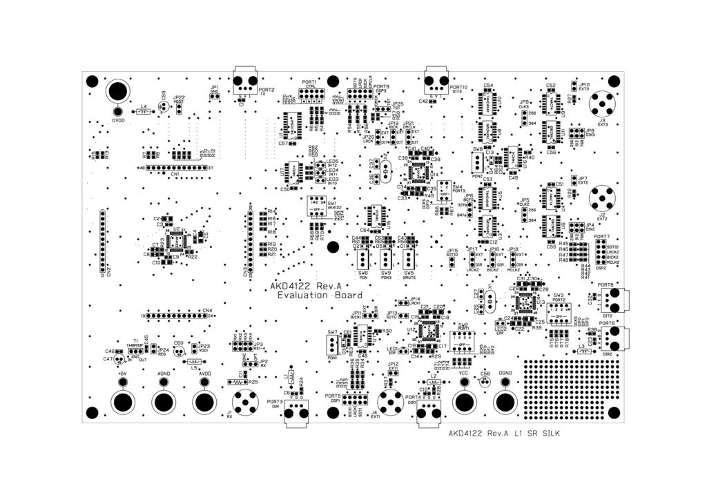
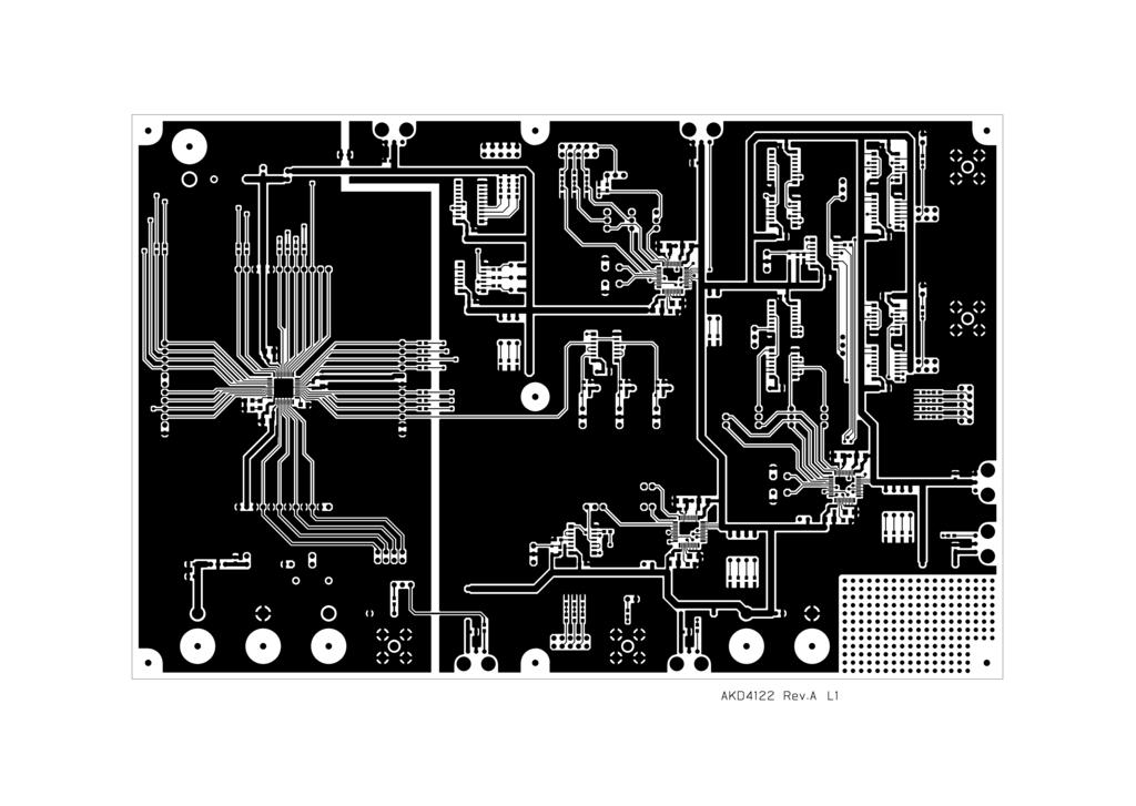
1 [K4-] K4- valuation board Rev.0 for K4 GNRL SRIPTION The K4- is an evaluation board for the digital sample rate converter, the K4 with built-in digital audio interface receiver (). The K4- has the digital audio interface and can achieve the interface with digital audio system via opt-connector. Ordering guide K valuation board for K4 (able for connecting with printer port of IM-T compatible P and control software are packed with this. This control software does not operate on Windows NT.) FUNTION /IT with optical input/output 0pin Header for KM / evaluation board N connector for an external clock input 0pin Header for serial control mode +5V V, V GN, GN Opt In K4 4 K44 Opt Out RG.V SP ata 0 pin Head er 0pi n Header SP ata K4 IK In l ock ivider MLK In igi tal In Opt In 0 pin Header ontrol ata MLK In lock i vi der 0pin H eader K44 Opt In Opt Out SP ata Figure. K4- lock iagram * ircuit diagram and P layout are attached at the end of this manual. - -
2 [K4-] valuation oard Manual Operation sequence ) Set up the power supply lines. [V] (red) =.0.V (typ..v, V pin) [V] (red) =.0.V (typ..v, V pin) [+5V] (orange) = +5V (for regulator) [V] (blue) =.0.V (typ..v, for digital logic) [GN] (black) = 0V [GN] (black) = 0V ach supply line should be distributed from the power supply unit. ) Set up the evaluation mode, jumper pins. (See the followings.) ) Power on. The K4 should be reset once bringing SW (PN) L upon power-up. valuation mode I/O ports and jumper pins on the board should be set according to the following explanation in order to evaluate each pass of the K4. The block diagram is shown in Figure. MKO INT0 INT INT R FILT RX RX RX RX RX4 RX RX RX4 OPS-0 TX TX PN IK LRK STI IK LRK STI PORT Serial udio I/F IPS-0 ISL-0 e-em Filter SR YPS OSL PORT Serial udio I/F LRK IK STO SMUT LRK IK STO PORT PLL OMLK IK LRK STIO IK LRK STIO Serial udio I/F M/S M/S MLK ontrol Register MK V VSS V VSS TO TI LK SN Figure. K4 lock iagram - -
3 [K4-] () K4 PORT SR K4 PORT Refer to page 5 for input port setting, and page 5 8 for output port setting. PORT4 U K44 U4 K44 PORT0 IT K4 PORT5 SP IK LRK ST I IK LRK STO OMLK PORT9 SP J4 ivider J Figure. K4 PORT SR K4 PORT () K4 PORT SR K4 PORT Refer to page 9 for input port setting, and page 5 8 for output port setting. PORT U K44 U4 K44 PORT0 IT K4 IK IK PORT7 SP LRK ST IO LRK STO PORT9 SP MLK OMLK J ivider ivider J Figure 4. K4 PORT SR K4 PORT () K4 SR K4 PORT Refer to page 0 for input port setting, and page 5 8 for output port setting. U4 K44 PORT0 IT PORT K4 RX I K RX LR K RX ST O PORT9 SP J RX RX4 OMLK ivider J Figure 5. K4 SR K4 PORT - -
4 [K4-] (4) K4 PORT SR K4PORT Refer to page 5 for input port setting, and page 4 for output port setting. PORT4 U K44 U K44 PORT8 IT K4 PORT5 SP IK LRK ST I IK LRK ST IO MLK PORT7 SP J4 ivider J Figure. K4 PORT SR K4 PORT (5) K4 SR K4 PORT Refer to page 0 for input port setting, and page 4 for output port setting. U K44 PORT8 IT PORT K4 RX IK RX LRK RX STIO PORT7 SP J RX RX4 MLK ivider J Figure 7. K4 SR K4 PORT () ypass Mode Refer to page 5 0 for input port setting, and output port setting should be master mode. The bypass mode of the K4 is set by the register. In bypass mode, the IT function of the K44 can not be used as the output port. 0pin PORT should be used instead. Input IK, LRK, and T are output from the output port side in the bypass mode
5 [K4-] () Setting for Input port (K4 PORT) (-) Slave Mode. When using function of K44 (U) When using PORT4 (), nothing should be connected to J4 () and PORT5 (SP). JP () should be short. JP IK JP JP STO JP4 LRK SW setting (See Table,Table ) Upper-side is H and lower-side is L. SW No. Name ON ( H ) OFF ( L ) OKS Fixed to L IF0 IF 4 IF K44 udio Format Setting Refer to Table Table. SW setting Mode udio I/F Format K44 K4 IF IF IF0 IF IF0 0 bit, LS justified bit, MS justified efault 4bit, I S ompatible 0 0 4bit, LS justified 0 Table. K44 udio interface format setting * IF-0 of the K4 is set by the register.. When connecting with the serial interface of UP, ROH & SHWRZ When using PORT5 (SP), nothing should be connected to PORT4 (). IK is input from J4 (), and the LRK and STI are supplied from UP. JP () should be open. JP IK JP JP STO JP4 LRK. ll clocks are fed through the 0pin port When using PORT5 (SP), nothing should be connected to J4 () and PORT4 (). JP () should be short. JP IK JP JP STO JP4 LRK - 5 -
6 [K4-] () Setting for Input port (K4 PORT) (-) Slave mode. When using function of K44 (U) When using PORT (), nothing should be connected to J () and PORT7 (SP). Set JP8 (MLK) to the when MLK is supplied to the K4. JP5 STIO JP IK JP7 LRK JP8 MLK SW setting (See Table,Table 4,Table 5) Upper-side is H and lower-side is L. SW No. Name ON ( H ) OFF ( L ) K44 Master lock Output Setting OKS Refer to Table 4 IF0 IF 4 IF K44 udio Format Setting Refer to Table 5 Table. SW setting Mode OKS MKO X tal fs 0 0 5fs 5fs 9kHz efault 5fs 5fs 48kHz Table 4. K44 MKO setting Mode udio I/F Format K44 K4 IF IF IF0 IIF IIF0 0 bit, LS justified bit, MS justified efault 4bit, I S ompatible 0 0 4bit, LS justified 0 Table 5. K44 udio interface format setting * IIF-0 of the K4 is set by the register. - -
7 [K4-]. When connecting with the serial interface of UP, ROH & SHWRZ When using PORT7 (SP), nothing should be connected to PORT (). MLK is input from J (), IK is supplied by using the clock dividing circuit on this evaluation board and the LRK and STI are supplied from UP. Set JP8 (MLK) to the when MLK is supplied to the K4. JP5 STIO JP IK JP7 LRK JP8 MLK lock Setting MLK is input from J (), IK is supplied by using the clock dividing circuit. JP4 (IV) and JP5 (LK) are set by referring to Table. JP (FS) selects the frequency of IK. JP7 () should be open. JP4 IV JP5 LK JP FS JP fs fs fs MLK JP4(IV) JP5(LK) 5fs =.048MHz 5 5 8kHz 84fs =.07MHz Open 84 5fs = 4.09MHz fs =.44MHz fs = 8.9MHz 5 5 khz 84fs =.88MHz Open 84 5fs =.84MHz fs = 4.57MHz fs =.89MHz kHz 84fs =.944MHz Open 84 5fs =.579MHz fs =.888MHz fs =.88MHz kHz 84fs = 8.4MHz Open 84 5fs = 4.57MHz fs =.84MHz kHz 5fs =.579MHz fs =.888MHz Open 84 9kHz 5fs = 4.57MHz fs =.84MHz Open 84 Table. xample for lock setting - 7 -
8 [K4-]. ll clocks are fed through the 0pin port When using PORT7 (SP), nothing should be connected to J () and PORT (). JP7 () should be short. JP5 STIO JP IK JP7 LRK JP8 MLK (-) Master mode MLK must be provided in the master mode.. When using function of K44 (U) When using PORT (), nothing should be connected to J () and PORT7 (SP). Set JP8 (MLK) to the in order to supply MLK to the K4. JP5 STIO JP IK JP7 LRK JP8 MLK SW setting (See Table 7,Table 8,Table 9) Upper-side is H and lower-side is L. SW No. Name ON ( H ) OFF ( L ) K44 Master lock Output Setting OKS Refer to Table 8 IF0 IF 4 IF K44 udio Format Setting Refer to Table 9 Table 7. SW setting Mode OKS MKO X tal fs 0 0 5fs 5fs 9kHz 5fs 5fs 48kHz Table 8. K44 MKO setting Mode udio I/F Format K44 K4 IF IF IF0 IIF IIF0 0 4bit, MS justified 0 0 4bit, I S ompatible 0 Table 9. K44 udio interface format setting * IIF-0 of the K4 is set by the register
9 [K4-]. ll clocks are fed through the 0pin port When using PORT7 (SP), nothing should be connected to J () and PORT (). JP7 () should be short. MLK is supplied to the K4, and the T that synchronizes with IK and LRK output from the K4 is supplied to the K4. JP5 STIO JP IK JP7 LRK JP8 MLK (-) SW setting Set SW according to the mode of the K4 PORT. SW No. Name ON ( H ) OFF ( L ) efault M/S Master Mode Slave Mode L M/S Master Mode Slave Mode L TST4 Fixed to L L Table 0. SW setting - 9 -
10 [K4-] () Setting for Input port (K4 ) (-) Setting for input The signal source of K4 s can be set by JP (RX) and JP (RX-4). V L 47u PORT V GN OUT OPT J RX R5 75 R4 470 JP RX N JP RX-4 RX RX RX RX4 RX RX RX RX4 Figure 8. input circuit JP RX JP RX JP RX-4 RX RX RX RX4 RX JP RX-4 Optical N RX N oaxial Figure 9. JP setting RX RX RX RX4 JP RX-4 RX RX RX RX4 JP RX-4 RX RX RX RX4 Figure 0. JP setting RX RX RX RX4 (-) Setting for through signal through signal of the K4 is output to TX pin via PORT (TX). TX V PORT IN V GN TX Figure. through signal - 0 -
11 [K4-] (4) Setting for Output port (K4 PORT) (4-) Slave mode. When using IT function of K44 (U) When using X tal (X) and PORT8 (IT), nothing should be connected to PORT () and PORT7 (SP). Set JP8 (MLK) to the when MLK is supplied to the K4. When MLK frequency is changed, the value of X tal (X) frequency should be changed according to MLK frequency. JP5 STIO JP IK JP7 LRK JP8 MLK SW setting (See Table,Table,Table ) Upper-side is H and lower-side is L. SW No. Name ON ( H ) OFF ( L ) K44 Master lock Output Setting OKS Refer to Table IF0 IF 4 IF K44 udio Format Setting Refer to Table Table. SW setting Mode OKS MKO X tal fs 0 0 5fs 5fs 9kHz efault 5fs 5fs 48kHz Table. K44 MKO setting Mode udio I/F Format K44 K4 IF IF IF0 IIF IIF0 0 4bit, MS justified bit, MS justified efault 4bit, I S ompatible 0 0 4bit, MS justified 0 0 Table. K44 udio interface format setting * IIF-0 of the K4 is set by the register. - -
12 [K4-]. When connecting with the serial interface of UP, ROH & SHWRZ When using PORT7 (SP), nothing should be connected to PORT (). MLK is input from J (), IK and LRK are supplied by using the clock dividing circuit on this evaluation board to the K4. Set JP8 (MLK) to the when MLK is supplied to the K4. JP5 STIO JP IK JP7 LRK JP8 MLK lock Setting MLK is input from J (), IK and LRK are generated by using the clock dividing circuit. JP4 (IV) and JP5 (LK) are set by referring to Table 4. JP (FS) selects the frequency of IK. JP7 () should be open. JP4 IV JP5 LK JP FS JP fs fs fs MLK JP4(IV) JP5(LK) 5fs = 8.9MHz 5 5 khz 84fs =.88MHz Open 84 5fs =.84MHz fs = 4.57MHz fs =.89MHz kHz 84fs =.944MHz Open 84 5fs =.579MHz fs =.888MHz fs =.88MHz kHz 84fs = 8.4MHz Open 84 5fs = 4.57MHz fs =.84MHz kHz 5fs =.579MHz fs =.888MHz Open 84 9kHz 5fs = 4.57MHz fs =.84MHz Open 84 Table 4. xample for lock setting. ll clocks are fed through the 0pin port When using PORT7 (SP), nothing should be connected to J () and PORT (). JP7 () should be short. JP5 STIO JP IK JP7 LRK JP8 MLK - -
13 [K4-] (4-) Master mode MLK must be provided in the master mode.. When using IT function of K44 (U) When using X tal (X) and PORT8 (IT), nothing should be connected to PORT () and PORT7 (SP). Set JP8 (MLK) to the when MLK is supplied to the K4. When MLK frequency is changed, the value of X tal (X) frequency should be changed according to MLK frequency. JP5 STIO JP IK JP7 LRK JP8 MLK SW setting (See Table 5,Table,Table 7) Upper-side is H and lower-side is L. SW No. Name ON ( H ) OFF ( L ) K44 Master lock Output Setting OKS Refer to Table IF0 IF 4 IF K44 udio Format Setting Refer to Table 7 Table 5. SW setting Mode OKS MKO X tal fs 0 0 5fs 5fs 9kHz 5fs 5fs 48kHz Table. K44 MKO setting Mode udio I/F Format K44 K4 IF IF IF0 IIF IIF0 0 4bit, MS justified 0 0 4bit, I S ompatible 0 Table 7. K44 udio interface format setting * IIF-0 of the K4 is set by the register. - -
14 [K4-]. When connecting with the serial interface of UP, ROH & SHWRZ When using PORT7 (SP), nothing should be connected to PORT () and PORT8 (IT). MLK is input from J (), IK LRK, and T are supplied from the K4. Set JP8 (MLK) to the in order to supply MLK to the K4. JP5 STIO JP IK JP7 LRK JP8 MLK lock Setting MLK is input from J (). JP7 () should be open. JP4 IV JP5 LK JP FS JP fs fs ll clocks are fed through the 0pin port When using PORT7 (SP), nothing should be connected to J (), PORT () and PORT8 (IT). JP7 () should be short. MLK is supplied to the K4, and IK, LRK and T are supplied from the K4. JP5 STIO JP IK JP7 LRK JP8 MLK (4-) SW setting Set SW according to the mode of the K4 PORT. SW No. Name ON ( H ) OFF ( L ) efault M/S Master Mode Slave Mode L M/S Master Mode Slave Mode L TST4 Fixed to L L Table 8. SW setting - 4 -
15 [K4-] (5) Setting for Output port (K4 PORT) (5-) Slave mode. When using IT function of K44 (U4) When using X tal (X) and PORT0 (IT), nothing should be connected to PORT9 (SP). Please set JP (OMLK) to the IT when MLK is supplied to the K4. When MLK frequency is changed, the value of X tal (X) frequency should be changed according to MLK frequency. JP9 IK JP0 LRK JP OMLK JP5 TST IT IT IT OMK TST SW4 setting (See Table 9,Table 0,Table ) Upper-side is H and lower-side is L. SW4 No. Name ON ( H ) OFF ( L ) OKS K44 Master lock Output Setting Refer to Table 0 IF0 K44 udio Format Setting Refer to Table Table 9. SW4 setting Mode OKS MKO X tal fs 0 0 5fs 5fs 9kHz efault 5fs 5fs 48kHz Table 0. K44 MKO setting Mode udio I/F Format K44 K4 IF0 OIF 0 4bit, MS justified 0 0 efault 4bit, I S ompatible Table. K44 udio interface format setting * OIF of the K4 is set by the register
16 [K4-]. When connecting with the serial interface of UP, ROH & SHWRZ When using PORT9 (SP), nothing should be connected to PORT0 (IT). MLK is input from J (), IK and LRK are supplied by using the clock dividing circuit on this evaluation board to the K4. Set JP (OMLK) to the when MLK is supplied to the K4. JP9 IK JP0 LRK JP OMLK JP5 TST IT IT IT OMK TST lock Setting MLK is input from J (), IK and LRK are generated by using the clock dividing circuit. JP8 (IV) and JP9 (LK) are set by referring to Table. JP0 () should be open. JP8 IV JP9 LK JP fs MLK JP8(IV) JP9(LK) 5fs = 8.9MHz 5 5 khz 84fs =.88MHz Open 84 5fs =.84MHz fs = 4.57MHz fs =.89MHz kHz 84fs =.944MHz Open 84 5fs =.579MHz fs =.888MHz fs =.88MHz kHz 84fs = 8.4MHz Open 84 5fs = 4.57MHz fs =.84MHz kHz 5fs =.579MHz fs =.888MHz Open 84 9kHz 5fs = 4.57MHz fs =.84MHz Open 84 Table. xample for lock setting. ll clocks are fed through the 0pin port When using PORT9 (SP), nothing should be connected to PORT0 (IT). Set JP5 (TST) to the OMK when MLK is supplied to the K4. JP0 () should be short. JP9 IK JP0 LRK JP OMLK JP5 TST IT IT IT OMK TST - -
17 [K4-] (5-) Master mode MLK must be provided in the master mode.. When using IT function of K44 (U4) When using X tal (X) and PORT0 (IT), nothing should be connected to PORT9 (SP). Set JP (OMLK) to the IT in order to supply MLK to the K4. When MLK frequency is changed, the value of X tal (X) frequency should be changed according to MLK frequency. JP9 IK JP0 LRK JP OMLK JP5 TST IT IT IT OMK TST SW4 setting (See Table,Table 4,Table 5) Upper-side is H and lower-side is L. SW4 No. Name ON ( H ) OFF ( L ) OKS K44 Master lock Output Setting Refer to Table 4 IF0 K44 udio Format Setting Refer to Table 5 Table. SW4 setting Mode OKS MKO X tal fs 0 0 5fs 5fs 9kHz 5fs 5fs 48kHz Table 4. K44 MKO setting Mode udio I/F Format K44 K4 IF0 OIF 0 4bit, MS justified 0 0 4bit, I S ompatible Table 5. K44 udio interface format setting * OIF of the K4 is set by the register
18 [K4-]. When connecting with the serial interface of UP, ROH & SHWRZ When using PORT9 (SP), nothing should be connected to PORT0 (IT). MLK is input from J (), IK LRK, and T are supplied from the K4. Set JP (OMLK) to the in order to supply MLK to the K4. JP9 IK JP0 LRK JP OMLK JP5 TST IT IT IT OMK TST lock Setting MLK is input from J (). JP0 () should be open. JP8 IV JP9 LK JP ll clocks are fed through the 0pin port When using PORT9 (SP), nothing should be connected to J () and PORT0 (IT). Set JP5 (TST) to the OMK in order to supply MLK to the K4. JP0 () should be short. MLK is supplied to the K4, and IK, LRK and T are supplied from the K4. JP9 IK JP0 LRK JP OMLK JP5 TST IT IT IT OMK TST (5-) SW setting Set SW according to the mode of the K4 PORT. SW No. Name ON ( H ) OFF ( L ) efault M/S Master Mode Slave Mode L M/S Master Mode Slave Mode L TST4 Fixed to L L Table. SW setting - 8 -
19 [K4-] Other jumper pins set up. JP (GN) : nalog ground and igital ground OPN: Separated. SHORT: ommon. (The connector GN can be open.) <efault>. JP (V) : V and V OPN: Separated. SHORT: ommon. (The connector V can be open.) <efault>. JP (V) : V and V OPN: Separated. SHORT: ommon. (The connector V can be open.) <efault> 4. JP4 (RG) : +5V and V OPN: Separated. SHORT: ommon. (The connector V can be open.) <efault> The regulator can be supplied.v to all circuits by shorting JP, and 4 and supplying 5V to +5V connector. The function of the toggle SW Upper-side is H and lower-side is L. [SW5] (SMUT): Soft mute of K4 [SW] (PN): Resets the K4. Keep H during normal operation. The K4 should be resets once bringing L upon power-up. [SW7] (PN): Resets the K44 (U). Keep H during normal operation. The K44 (U) should be resets once bringing L upon power-up. Keep L when K44 (U) is not used. [SW8] (PN): Resets the K44 (U). Keep H during normal operation. The K44 (U) should be resets once bringing L upon power-up. Keep L when K44 (U) is not used. [SW9] (PN): Resets the K44 (U4). Keep H during normal operation. The K44 (U4) should be resets once bringing L upon power-up. Keep L when K44 (U4) is not used
20 [K4-] Indication for L [L] (RF): Monitor INT0 pin of the K44 (U). L turns on when unlock or parity error occurs. [L] (RF): Monitor INT0 pin of the K44 (U). L turns on when unlock or parity error occurs. [L] (INT0): Monitor INT0 pin of the K4. [L4] (INT): Monitor INT pin of the K4. [L5] (INT): Monitor INT pin of the K4. Serial ontrol The K4 can be controlled via the printer port (parallel port) of IM-T compatible P. onnect PORT (TRL) with P by 0 wire flat cable packed with the K4-. 0 P onnect SN LK TI K4- TO 0 Wire Flat able 5 0pin onnector 0pin Header Figure. onnection of 0 wire flat cable - 0 -
21 [K4-] ontrol Software Manual Set-up of evaluation board and control software. Set up the K4- according to previous term.. onnect IM-T compatible P with K4- by 0-line type flat cable (packed with K4-). Take care of the direction of 0pin header. (Please install the driver in the -ROM when this control software is used on Windows 000/XP. Please refer Installation Manual of ontrol Software river by KM device control software. In case of Windows95/98/M, this installation is not needed. This control software does not operate on Windows NT.). Insert the -ROM labeled K4 valuation Kit into the -ROM drive. 4. ccess the -ROM drive and double-click the icon of K4-.exe to set up the control program. 5. Then please evaluate according to the follows. Operation flow Keep the following flow.. Set up the control program according to explanation above.. lick Port Setup button.. lick Write default button. Then set up the dialog and input data. xplanation of each buttons. [Port Setup] : Set up the printer port.. [Write default] : Initialize the register of K4.. [ll Read] : Read the all register of K4. 4. [Function] : ialog to write data by keyboard operation. 5. [Write] : ialog to write data by mouse operation.. [Read] : Read each register data by mouse operation. xplanation of each dialog. [Function ialog] : ialog to write data by keyboard operation ddress ox: ata ox: Input register address in figures of hexadecimal. Input register data in figures of hexadecimal. If you want to write the input data to K4, click OK button. If not, click ancel button.. [Write ialog] : ialog to write data by mouse operation There are dialogs corresponding to each register. lick the Write button corresponding to each register to set up the dialog. If you check the check box, data becomes H or. If not, L or 0. If you want to write the input data to K4, click OK button. If not, click ancel button. - -
22 [K4-] Indication of data Input data is indicated on the register map. Red letter indicates H or and blue one indicates L or 0. lank is the part that is not defined in the datasheet. - -
23 [K4-] MSURMNT RSULTS [Measurement condition] Measurement unit : udio Precision, System Two ascade Power Supply : V = V =.V and width : 0Hz FSO/ Temperature : Room Measurement Path : K4 PORT SR K4 PORT [Measurement Result] SR haracteristics Result Unit TH+N (Input = khz, 0dFS) FSO/FSI = 44.kHz/48kHz FSO/FSI = 48kHz/44.kHz FSO/FSI = khz/48khz FSO/FSI = 9kHz/kHz Worst ase (FSO/FSI = 48kHz/8kHz) d d d d d ynamic Range (Input = khz, 0dFS) FSO/FSI = 44.kHz/48kHz FSO/FSI = 48kHz/44.kHz FSO/FSI = khz/48khz FSO/FSI = 9kHz/kHz Worst ase (FSO/FSI = khz/44.khz) ynamic Range (Input = khz, 0dFS, -weighted) FSO/FSI = 44.kHz/48kHz d d d d d d - -
24 [K4-] [Plots] -00 K4 TH + N vs Input Level FSI = 44.kHz, SFO = 48kHz, fin = khz d F S akd4a.at7 Figure. TH+N vs. Input Level d F S K4 TH + N vs Input Frequency FSI = 44.kHz, SFO = 48kHz, Input = 0dFS akd4a.at7 Figure 4. TH+N vs. Input Frequency (Input = 0dFS) - 4 -
25 [K4-] d F S K4 TH + N vs Input Frequency FSI = 44.kHz, SFO = 48kHz, Input = -0dFS akd4a.at7 Figure 5. TH+N vs. Input Frequency (Input = -0dFS) +0 K4 Linearity FSI = 44.kHz, SFO = 48kHz, fin = khz d F S akd4a.at7 Figure. Linearity - 5 -
26 [K4-] d F S K4 Frequency Response FSI = 44.kHz, SFO = 48kHz, Input = 0dFS akd4a.at7 d F S Figure 7. Frequency Response K4 FFT FSI = 44.kHz, SFO = 48kHz, Input = 0dFS, fin = khz akd4a.at7 Figure 8. FFT Plot (Input = 0dFS) - -
27 [K4-] +0 K4 FFT FSI = 44.kHz, SFO = 48kHz, Input = -0dFS, fin = khz d F S akd4a.at7 Figure 9. FFT Plot (Input = -0dFS) - 7 -
28 [K4-] RVISION HISTORY ate Manual oard Reason Page ontents (yy/mm/dd) Revision Revision 09/0/0 KM First dition IMPORTNT NOTI These products and their specifications are subject to change without notice. When you consider any use or application of these products, please make inquiries the sales office of sahi Kasei M orporation (KM) or authorized distributors as to current status of the products. KM assumes no liability for infringement of any patent, intellectual property, or other rights in the application or use of any information contained herein. ny export of these products, or devices or systems containing them, may require an export license or other official approval under the law and regulations of the country of export pertaining to customs and tariffs, currency exchange, or strategic materials. KM products are neither intended nor authorized for use as critical components Note) in any safety, life support, or other hazard related device or system Note), and KM assumes no responsibility for such use, except for the use approved with the express written consent by Representative irector of KM. s used here: Note) critical component is one whose failure to function or perform may reasonably be expected to result, whether directly or indirectly, in the loss of the safety or effectiveness of the device or system containing it, and which must therefore meet very high standards of performance and reliability. Note) hazard related device or system is one designed or intended for life support or maintenance of safety or for applications in medicine, aerospace, nuclear energy, or other fields, in which its failure to function or perform may reasonably be expected to result in loss of life or in significant injury or damage to person or property. It is the responsibility of the buyer or distributor of KM products, who distributes, disposes of, or otherwise places the product with a third party, to notify such third party in advance of the above content and conditions, and the buyer or distributor agrees to assume any and all responsibility and liability for and hold KM harmless from any and all claims arising from the use of said product in the absence of such notification
29 V V PORT TRL SN LK TI TO R 47k R 47k R 47k R4 470 R5 470 R 470 U Y Y 4 Y 5 4 Y4 5 Y5 7 Y 8 7 Y7 9 8 Y8 G 9 G 74LV N 48 R R OMLK 4 R9 5 LRK 4 IK STO R0 R R INT 8 INT0 7 V PORT IN V GN TX 0u U TI LK 48 SN 47 VSS 4 V 45 VSS 44 + R 5 N OMLK 4 LRK 4 IK 4 STO 40 TX 9 8 INT 7 INT0 STIO N R4 5 STIO R5 5 TO IK 5 5 R 5 IK TST TST LRK 4 4 R7 5 LRK V INT 4 4 INT MLK R8 5 MLK PORT-IF R8 R9 R70 47K 47K 47K M/S M/S TST4 SW K TST TST M/S M/S K4 V VSS STI 0 IK u 0 9 R9 5 R0 5 STI IK SMUT 9 9 SMUT LRK 8 8 R 5 LRK V 0 0 TST4 PN 7 7 PN PORT V GN OUT J RX L 47u R4 470 OPT JP RX JP RX RX RX RX4 RX-4 RX RX RX RX4 7.n R u TST5 FILT N4 VSS 9 0 0u 4 V + TST 5 RX 7 TST7 8 RX TST8 9 0 RX TST9 RX4 TST0 TST 4 VSS R 5 R k 5 JP GN nalog Ground igital Ground R5 75 N V RX RX RX RX4 Title K4- Size ocument Number Rev K4 0 ate: Monday, March, 009 Sheet of - 9 -
30 V For K4 PORT J R 5 JP7 LK PR 0 L U Q 9 Q 8 U Q 4 4 Q 5 Q Q RO 5 7 NP 0 NT LK 9 LO LR 74 PR 4 Q 5 JP4 5 5 LK U5 5 JP5 0 4fs 78 Q LK Q 9 LK Q 7 RST Q IV 84 Q4 5 fs Q5 Q Q7 4 fs Q8 Q9 Q0 4 Q 5 Q 74H4040 L U JP FS U G V 4 GN 7 4 G Y 5 0 G Y 9 Y 8 4G 4 4Y 74VH5 V -MLK -IK -LRK U 74H4 V U8 V For K4 PORT J R7 5 JP0 LK PR 0 L U 4 5 U Q 9 Q 8 Q 4 Q Q Q RO 5 7 NP 0 NT LK 9 LO LR 74 PR 4 U Q 5 JP8 5 5 LK U0 5 JP9 0 LK Q 9 4fs 78 Q LK Q 7 RST Q IV 84 Q4 5 Q5 Q Q7 4 fs Q8 Q9 Q0 4 Q 5 Q 74H4040 L G V 4 GN 7 4 G Y 5 0 G Y 9 Y 8 4G 4 4Y 74VH5 -MLK -IK -LRK 4 U 74H4 Title K4- Size ocument Number Rev xternal lock 0 ate: Monday, March, 009 Sheet of - 0 -
31 V V HSU9 R 0k PORT4 V GN OUT 5 L 47u + 4 0u SW7 PN L H 0 U7 74H4 9 8 U7 74H4 44-PN R u R9 8k PORT-IF0 U IPS0 N IF0 4 TST 48 RX N 47 4 RX U7 5 74H4 R0 L k RF PORT-OKS IK LRK STI IK LRK STI PORT SP PORT-IF 44-PN PORT-IF JP IK 9 OKS IF0 IF IF 4 V 0u R7 R7 R7 R74 47K 47K 47K 47K PORT-OKS PORT-IF0 PORT-IF PORT-IF Title K4- Size ocument Number Rev PORT 0 ate: Monday, March, 009 Sheet of + 45 TST 44 RX N 4 4 RX0 VSS 4 VOM 40 R 9 V 8 7 INT INT0 OKS0 OKS M 5 4 R 00 R 00 R 00 5 IF M0 R4 0k R5 0k R 0k N K44 PN 7 IF XTI 0 8 IPS XTO 9 U7 74H4 4 U7 74H4 9 0 P/SN XTL0 UX 8 MKO 7 XTL VIN TV VSS 8 + J4 R7 5 JP 4 TX0 5 TX OUT 7 OUT 8 UOUT 9 VOUT 0 V VSS MKO 4 LRK IK STO 5 JP STO JP4 LRK SW PORT u U7F 74H4 - -
32 V V PORT V GN OUT L 47u R u u R9 8k SW8 PN 4 HSU9 L H R4 0k 0 U 74H4 9 8 U 74H4 44-PN U IPS0 48 RX N 47 4 RX 45 TST 44 RX N 4 4 RX0 VSS 4 VOM 40 R 9 V 8 7 INT INT0 U 74H4 5 R40 k L RF PORT-IF0 PORT-IF PORT-IF N IF0 TST IF N IF IPS P/SN K44 OKS0 5 OKS 4 M M0 PN XTI 0 XTO 9 UX 8 PORT-OKS 44-PN p X.89MHz 7 p MLK IK LRK STIO R45 0k R4 0k R47 0k R4 00 R4 00 R4 00 R44 00 R48 0k MLK IK LRK STIO PORT SP 0 XTL0 XTL VIN TV VSS 8 4 TX0 5 TX OUT 7 OUT 8 UOUT 9 VOUT 0 V VSS 9 MKO 4 LRK MKO 7 IK STO 5 JP5 STIO JP IK -IK R75 R7 R77 R78 47K 47K 47K 47K OKS IF0 IF IF 4 SW PORT V PORT-OKS PORT-IF0 PORT-IF PORT-IF 0 0u 0u JP7 LRK PORT8 IN V GN IT + + UF 74H4 JP8 MLK -LRK -MLK Title K4- Size ocument Number Rev PORT 0 ate: Monday, March, 009 Sheet 4 of - -
33 V V + 0u 5 HSU9 R5 0k u R49 8k SW9 PN L H U5 74H4 4 U5 74H4 44-PN U4 IPS0 48 RX N 47 4 RX 45 TST 44 RX N 4 4 RX0 VSS 4 VOM 40 R 9 V 8 7 INT INT0 TST JP5 TST TST PORT-IF0 PORT-IF N IF0 TST IF N IF IPS P/SN K44 OKS0 5 OKS 4 PORT-OKS M M0 PN 44-PN p XTI 0 X 4.57MHz XTO 9 7 p UX 8 OMLK IK LRK STO R54 0k R55 0k R5 0k R50 00 R5 00 R5 00 R5 00 R57 0k OMK PORT9 OMLK 0 IK LRK 9 8 STO SP 0 XTL0 MKO 7 XTL IK IT VIN TV VSS TX0 TX OUT OUT UOUT VOUT V VSS MKO LRK STO 5 JP9 IK -IK OKS IF0 SW4 PORT 4 V IT R R7 47K 47K PORT-OKS PORT-IF0 40 0u 4 0u JP0 LRK PORT0 IN V GN IT IT JP OMLK -LRK -MLK - - Title K4- Size ocument Number Rev PORT 0 ate: Monday, March, 009 Sheet 5 of
34 V HSU9 R58 0k SW5 SMUT L H 4 5 U5 74H4 9 8 U5 74H4 SMUT V L INT0 R59 k U7 74H4 INT0 V L4 INT R0 k 4 U7 74H4 INT HSU9 R 0k INT SW PN L H PN L5 INT R k 5 U7 74H4 44 U5F 74H4 0 U5 74H4 V V V +5V U7 74H For 74H4 x 4, 74H4040 x, 7474 x, 74 x, 74LV54 x u + JP V V 59 47u + L4 (short) JP V V L5 (short) u JP4 RG 45 T T48MF OUT GN IN u + U7 74H4 0 U7F 74H4 Title K4- Size ocument Number Rev 0 Power Supply ate: Monday, March, 009 Sheet of - 4 -
35 - 5 -
36 - -
37 - 7 -
Single Clock Generator
 ASAHI KASEI EMD CORPORATION Single Clock Generator AK8113 Features Output Frequency Range: 74.17582MHz / 74.25MHz (Selectable) Input Frequency: 27MHz Low Jitter Performance: 15 ps (Typ.) Period, 1σ Low
IR1011 Photovoltaic Infrared Sensor
 IR1011 Photovoltaic Infrared Sensor GENERAL DESCRIPTION IR1011 is the world smallest mid-infrared quantum photo diode, made of InSb. This surface mount type sensor can be operated at room temperature,
EM-3242 One-chip monolithic Rotation Angle Sensor Preliminary Specification
 EM-3242 One-chip monolithic Rotation Angle Sensor Preliminary Specification Characteristics These specifications are subject to change without notice Rotation Angle Sensor Device with Hall Element Inside
Output Coupling Capacitor-less Video Amp with LPF
 AK4250 Output Coupling Capacitorless Video Amp with LPF GENERAL DESCRIPTION The AK4250 is a Video Amp with LPF. The output coupling capacitor can be removed because the AK4250 includes the negative power
Spread Spectrum Clock Generator AK8126
 Spread Spectrum Clock Generator AK8126 Features Output Frequency Range: 16MHz 128MHz Configurable Spread Spectrum Modulation: - AKEMD s Original Spread Spectrum Profile - Modulation Ratio: Center Spread:
Spread Spectrum Clock Generator
 ASAHI KASEI EMD CORPORATION Features Output Frequency Range: 90MHz 128MHz 1X or Convert 27MHz to 100MHz (3.7X) Configurable Spread Spectrum Modulation: - AKEMD s Original Spread Spectrum Profile - Modulation
Absolute Maximum Ratings. Note) Stresses beyond these listed values may cause permanent damage to the device. Operating Conditions
 Stresses beyond these listed values may cause permanent damage to the device. Operating Conditions") MS-0082 Semiconductor Magnetoresistive Element Semiconductor Magnetoresistive Element Composition MS-0082 is used as rotation sensor for gear (module: M=0.8), combining bias magnet. MS-0082 generates A/B
MS-0082 Semiconductor Magnetoresistive Element Semiconductor Magnetoresistive Element Composition MS-0082 is used as rotation sensor for gear (module: M=0.8), combining bias magnet. MS-0082 generates A/B
Spread Spectrum Clock Generator
 Spread Spectrum Clock Generator AK8125AE Features Input Frequency: - Crystal: 6.1-36MHz - External: 6.1-49.92MHz Configurable Spread Spectrum Modulation: - Modulation Ratio: -0.25%,-0.5%,-1.5%, -3.0% ±0.125%,±0.25%,±0.75%,
2.5V, 3.3V LVCMOS 1:18 Clock Fanout Buffer
 2.5V, 3.3V LVCMOS 1:18 Clock Fanout Buffer Features 18 LVCMOS outputs enable to drive up to 36 clock lines LVCMOS/LVTTL input 2.5V or 3.3V power supply Clock output frequency up to 200MHz Output-to-output
Features. Support for external one-path, internal three-path D/A converter reference voltages
 AK2330 DAC Type 8-bit 8-channel Electronic Volume Features 8-bit 8 channels of built-in multiplication D/A converters Support for external one-path, internal three-path D/A converter reference voltages
AK4204. Stereo Cap-less LINE-Amp and Video-Amp
 AK4204 Stereo Cap-less LINE-Amp and Video-Amp GENERAL DESCRIPTION The AK4204 is an audio stereo cap-less line driver with 1-channel video driver. It eliminates the need for large DC-blocking capacitors
[AKD570-A] Board Outline Chart Outline Chart J J J JP JP5 JP SW JP JP JP9 J6 T T JP JP JP6 T T JP0 U JP SW JP SW U U JP7 JP8 Port Port J5 J J7 J8 Figu
![[AKD570-A] Board Outline Chart Outline Chart J J J JP JP5 JP SW JP JP JP9 J6 T T JP JP JP6 T T JP0 U JP SW JP SW U U JP7 JP8 Port Port J5 J J7 J8 Figu](/thumbs/90/103721021.jpg "[AKD570-A] Board Outline Chart Outline Chart J J J JP JP5 JP SW JP JP JP9 J6 T T JP JP JP6 T T JP0 U JP SW JP SW U U JP7 JP8 Port Port J5 J J7 J8 Figu") [AKD570-A] AK570 Evaluation Board Rev. GENERA DESCRIPTION AKD570-A is an evaluation board for AK570 which is low voltage bit analog-digital converter developed for digital audio system. It supports Jacks
[AKD570-A] AK570 Evaluation Board Rev. GENERA DESCRIPTION AKD570-A is an evaluation board for AK570 which is low voltage bit analog-digital converter developed for digital audio system. It supports Jacks
AK4201. Stereo Cap-less HP-Amp
 AK4201 Stereo Cap-less HP-Amp GENERAL DESCRIPTION The AK4201 is an audio stereo cap-less headphone amplifier. The AK4201 eliminates the need for large DC-blocking capacitors with a built-in Charge-pump
Device Outline. Features
 AK7864A 3 channel LED driver with Charge Pump Device Outline This product includes the charge pump power supply and the 3 channel LED driver who drives the LED of the anode common in the constant current.
3.3V LVPECL 1:4. Features. Description. Block Diagram AK8181D
 Preliminary 3.3V LVPECL 1:4 Clock Fanout Buffer AK8181D Features Four differential 3.3V LVPECL outputs Selectable differential PCLK0p/n or LVPECL clock inputs PCLK0p/n pair can accept the following differential
AK dB 96kHz 24-Bit 2ch ΔΣ DAC
 AK4386 100dB 96kHz 24-Bit 2ch ΔΣ DAC GENERAL DESCRIPTION The AK4386 is a 24bit low voltage & low power stereo DAC. The AK4386 uses the Advanced Multi-Bit ΔΣ architecture, this architecture achieves DR=100dB
2.5V, 3.3V LVCMOS 1:9 Clock Fanout Buffer AK8180B
 2.5V, 3.3V LVCMOS 1:9 Clock Fanout Buffer AK8180B Features 9 LVCMOS outputs Selectable LVCMOS inputs 2.5V or 3.3V power supply Clock frequency up to 350MHz Output-to-output skew : 150ps max Synchronous
AK2929 Zero Drift operational amplifiers
 AK2929 Zero Drift operational amplifiers Feature AK2929 is the dual channel CMOS operational amplifires which is available to output with very low input offset voltage (+/- 1. V) and near zero input offset
2.5V, 3.3V LVCMOS 1:12 Clock Fanout Buffer AK8180C
 2.5V, 3.3V LVCMOS 1:12 Clock Fanout Buffer AK8180C Features 12 LVCMOS outputs Selectable LVCMOS and LVPECL inputs 2.5V or 3.3V power supply Clock frequency up to 350MHz Output-to-output skew : 150ps max
ARCHIVE INFORMATION. Freescale Semiconductor, I MECL PLL COMPONENTS 8/9, 16/17 DUAL MODULUS PRESCALER ARCHIVED BY FREESCALE SEMICONDUCTOR, INC.
 nc. Order this document by M226A/ The M226 is a high frequency, low voltage dual modulus prescaler used in phase locked loop (PLL) applications. The M226A can be used with MOS synthesizers requiring positive
OM29110 NFC's SBC Interface Boards User Manual. Rev May
 Document information Info Content Keywords Abstract OM29110, NFC, Demo kit, Raspberry Pi, BeagleBone, Arduino This document is the user manual of the OM29110 NFC s SBC Interface Boards. Revision history
MECL PLL COMPONENTS 64/65, 128/129 DUAL MODULUS PRESCALER
 Order this document by M222LVA/ The M222LVA can be used with MOS synthesizers requiring positive edges to trigger internal counters such as Motorola s M45XXX series in a PLL to provide tuning signals up
Direct Digital Synthesizers (DDS)
") pplication Note irect igital Synthesizers (S) Using the nalog evices 9 bit S to Generate Precision Frequencies in the range 0 to 0MHz and Precision ontiguous Phase hanges down to ns. 0L udubon Road, Wakefield,
pplication Note irect igital Synthesizers (S) Using the nalog evices 9 bit S to Generate Precision Frequencies in the range 0 to 0MHz and Precision ontiguous Phase hanges down to ns. 0L udubon Road, Wakefield,
LV5232VH. Specifications. Bi-CMOS IC 16ch LED Driver. Absolute Maximum Ratings at Ta = 25 C. Recommended Operating Conditions at Ta = 25 C
 Ordering number : ENA1628D LV5232VH Bi-MOS I 16ch LED Driver http://onsemi.com Overview The LV5232VH is a semiconductor integrated circuit that incorporates a serial input and serial or parallel output
LC75836WS-T/D. 1/4-Duty General-Purpose LCD Driver
 1/4-Duty General-Purpose LCD Driver Overview The LC75836WS-T is 1/4-duty general-purpose microprocessor-controlled LCD driver that can be used in applications such as frequency display in products with
AK4554 Low Power & Small Package 16bit Σ CODEC
 AK4554 Low Power & Small Package 16bit Σ CODEC GENERAL DESCRIPTION The AK4554 is a low voltage 16bit A/D & D/A converter for portable digital audio system. In the AK4554, the loss of accuracy form clock
LP3943/LP3944 as a GPIO Expander
 LP3943/LP3944 as a GPIO Expander General Description LP3943/44 are integrated LED drivers with SMBUS/I 2 C compatible interface. They have open drain outputs with 25 ma maximum output current. LP3943 has
LM48821 Evaluation Board User's Guide
 National Semiconductor Application Note 1589 Kevin Hoskins May 2007 Quick Start Guide from the two amplifiers found on pins OUTR and OUTL, respectively. Apply power. Make measurements. Plug in a pair of
Product Specification PE42540
 PE42540 Product Description The PE42540 is a HaRP technology-enhanced absorptive SP4T RF switch developed on UltraCMOS process technology. This switch is designed specifically to support the requirements
EVDP610 IXDP610 Digital PWM Controller IC Evaluation Board
 IXDP610 Digital PWM Controller IC Evaluation Board General Description The IXDP610 Digital Pulse Width Modulator (DPWM) is a programmable CMOS LSI device, which accepts digital pulse width data from a
SN54HC161, SN74HC161 4-BIT SYNCHRONOUS BINARY COUNTERS
 Internal Look-head for Fast ounting arry Output for n-it ascading Synchronous ounting Synchronously Programmable Package Options Include Plastic Small-Outline () and eramic Flat (W) Packages, eramic hip
AK V Single channel PCM CODEC LSI
 AK2300 3.3V Single channel PCM CODEC LSI GENERAL DESCRIPTION The AK2300 is a single channel PCM CODEC for various applications for example, AFE. It includes the selectable linear PCM interface, A/µ-law
PCAN-MicroMod Evaluation Test and Development Environment for the PCAN-MicroMod. User Manual. Document version ( )
") PCAN-MicroMod Evaluation Test and Development Environment for the PCAN-MicroMod User Manual Document version.0. (0-0-) Relevant products Product Name Part number Model PCAN-MicroMod Evaluation Board IPEH-000
PCAN-MicroMod Evaluation Test and Development Environment for the PCAN-MicroMod User Manual Document version.0. (0-0-) Relevant products Product Name Part number Model PCAN-MicroMod Evaluation Board IPEH-000
P3-HSI High Speed Isolated Sinking/Sourcing Input
 To minimize the risk of potential safety problems, you should follow all applicable local and national codes that regulate the installation and operation of your equipment. These codes vary from area to
Guardian and DL3282 Modem Interface Technical Service Application Note
 Guardian and DL3282 Modem Interface Technical Service Application Note OVERVIEW The following document is designed to provide information for the implementation of the Guardian Wireless Modem/Analog Radio
LC75836W/D. 1/4-Duty General-Purpose LCD Driver
 1/4-Duty General-Purpose LCD Driver Overview The LC75836W is 1/4-duty general-purpose microprocessor-controlled LCD driver that can be used in applications such as frequency display in products with electronic
CW308 UFO Target Board. On-board LC low-pass filter to provide clean power supply for resistive shunt measurement.
 NewE Technology NewE Technology Inc. newae.com hipwhisperer Embedded Security nalysis Tools Stand-lone Targets W0 UFO Target oard Product atasheet Get probing! The hipwhisperer W0 UFO board is the ultimate
AK4388A. 192kHz 24-Bit 2ch ΔΣ DAC
 AK4388A 192kHz 24Bit 2ch ΔΣ DAC GENERAL DESCRIPTION The AK4388A offers the perfect mix for cost and performance based audio systems. Using AKM's multi bit architecture for its modulator, the AK4388A delivers
8-Ch/Dual 4-Ch High-Performance CMOS Analog Multiplexers
 8-Ch/ual 4-Ch High-Performance CMOS Analog Multiplexers ESCRIPTION The G48 is an 8-channel single-ended analog multiplexer designed to connect one of eight inputs to a common output as determined by a
AK5358A. 96kHz 24-Bit ΔΣ ADC
 AK5358A 96kHz 24-Bit ΔΣ ADC GENERAL DESCRIPTION The AK5358A is a stereo A/D Converter with wide sampling rate of 8kHz 96kHz and is suitable for coumer to professional audio system. The AK5358A achieves
AK4180. Touch Screen Controller
 AK4180 Features: Sampling Frequency: 125kHz(max) Pen Pressure Measurement On-Chip Thermo Sensor Two Auxiliary Analog Inputs Direct Battery Measurement 4-wire I/F On-Chip Voltage Reference(2.5V) 12 bit
Single 8-Ch/Differential 4-Ch CMOS Analog Multiplexers (Obsolete for non-hermetic. Use DG408/409 as pin-for-pin replacements.)
") G58A_MIL/59A_MIL Single 8-Ch/ifferential -Ch CMOS Analog Multiplexers (Obsolete for non-hermetic. Use G8/9 as pin-for-pin replacements.) Low On-Resistance: 2 TTL and CMOS Logic Compatible Low Power: 3
G58A_MIL/59A_MIL Single 8-Ch/ifferential -Ch CMOS Analog Multiplexers (Obsolete for non-hermetic. Use G8/9 as pin-for-pin replacements.) Low On-Resistance: 2 TTL and CMOS Logic Compatible Low Power: 3
Video signal switcher
 Video signal switcher BA76N / BA76F The BA76N and BA76F are three-channel analog multiplexers with built-in mute, 6dB amplifier and 75Ω driver. The ICs designed for use in video cassette recorders, and
DatasheetArchive.com. Request For Quotation
 DatasheetArchive.com Request For Quotation Order the parts you need from our real-time inventory database. Simply complete a request for quotation form with your part information and a sales representative
KAPPA-T868SO. Smart Radio Telemetry Module
 KAPPA-T6 Smart Radio Telemetry Module Features Simple and low cost channel receiver module Range up to 500metres digital input/outputs Minimal external components Secure data protocol Ultra low power..6v
Hardware Guide. Control Made Simple. Model 401A Signal Generator
 Control Made Simple Model 401A Signal Generator Hardware Guide ON OFF LIMIT 1 2 3 4 RXD TXD POWER West Coast Office 1263 El Camino Real Menlo Park, CA 94025 Phone (650) 853-1444 Fax (650) 853-1405 www.flashcutcnc.com
AK4552 3V 96kHz 24Bit Σ CODEC
 AK4552 3V 96kHz 24Bit Σ CODEC GENERAL DESCRIPTION The AK4552 is a low voltage 24bit 96kHz A/D & D/A converter for digital audio system. In the AK4552, the loss of accuracy form clock jitter is also improved
DEMO MANUAL DC2326A LTC /18-Bit, Octal 200ksps, SAR ADC. Description. assembly options
 Description Demonstration circuit 2326A shows the proper way to drive the LTC 2345 ADC. The LTC2345 is a low noise, high speed, simultaneous sampling 16-/18-bit successive approximation register (SAR)
OBSOLETE. 9 khz. Operation Frequency 9 khz. db 6000 MHz. db Return Loss RF1, RF2 and RFC
 Product Description The PE455 RF Switch is designed to support the requirements of the test equipment and ATE market. This broadband general purpose switch maintains excellent RF performance and linearity
LOW POWER SCHOTTKY. GUARANTEED OPERATING RANGES ORDERING INFORMATION
 The SN74LS64 is a high speed 8-Bit Serial-In Parallel-Out Shift Register. Serial data is entered through a 2-Input AN gate synchronous with the LOW to HIGH transition of the clock. The device features
JEITA Part No. 4-pin power minimold (Pb-Free) Note 1 kpcs/reel CAUTION
 Note 1 kpcs/reel CAUTION") NPN Silicon RF Transistor for High-Frequency Low Distortion Amplifier 4-Pin Power Minimold FEATURES Low distortion: IM2 = 59.0 db TYP., IM3 = 82.0 db TYP. @, IC = 50 ma Low noise NF = 1.5 db TYP. @,
NPN Silicon RF Transistor for High-Frequency Low Distortion Amplifier 4-Pin Power Minimold FEATURES Low distortion: IM2 = 59.0 db TYP., IM3 = 82.0 db TYP. @, IC = 50 ma Low noise NF = 1.5 db TYP. @,
DF Absolute position, rotary Electric Encoder
 F-60-2017-02, May 2017 F-60-2 bsolute position, rotary lectric ncoder The F-60 is a member of the F series of lectric ncoders, based on Netzer Precision proprietary technology. The lectric ncoder offers
DEMO MANUAL DC2349A LTC5586 6GHz High Linearity I/Q Demodulator with Wideband IF Amplifier DESCRIPTION BOARD PHOTO
 DESCRIPTION Demonstration circuit 2349A showcases the LTC 5586 wideband high linearity IQ demodulator with IF amplifier. The Linear Technology USB serial controller, DC590B, is required to control and
Video signal switcher
 Video signal switcher BA76N / BA76F The BA76N and BA76F are three-channel analog multiplexers with built-in mute, 6dB amplifier and 7Ω driver. The ICs designed for use in video cassette recorders, and
High-Speed, Low-Glitch D/CMOS Analog Switches
 G6, G62, G63 High-Speed, Low-Glitch /CMOS Analog Switches ESCRIPTION The G6, G62, G63 feature high-speed lowcapacitance lateral MOS switches. Charge injection has been minimized to optimize performance
GPS Evaluation Kit EVA1035-H
 GPS Evaluation Kit EVA1035-H A Description of the Evaluation Board for Vincotech s GPS Receiver / Smart Antenna Module A1035-H User s Manual Version 1.0 Hardware Revision 01 Revision History Rev. Date
PC Tune PC Tune Test Procedures for 5100 Series Portable Radios
 PC Tune PC Tune Test Procedures for 5100 Series Portable Radios Part Number 002-9998-6513014 August 2008 Copyright 2006, 2007, 2008 by EFJohnson Technologies The EFJohnson Technologies logo, PC Configure,
RF V TO 4.0V, 470MHz to 510MHz TRANSMIT/RECEIVE MODULE
 3.3V to 4.0V, 470MHz to 510MHz Transmit/Receive Module 3.3V TO 4.0V, 470MHz to 510MHz TRNSMIT/REEIVE MODULE Package: LG, 8-Pin, 5.5mm x 5.0mm VReg V 1 8 7 6 5 4 3 Features Tx Output Power: 30dm Separate
NBXDBA V, 75 MHz / 150 MHz LVPECL Clock Oscillator
 . V, 75 MHz / 150 MHz LVPECL Clock Oscillator The NBXBA009 dual frequency crystal oscillator (XO) is designed to meet today s requirements for. V LVPECL clock generation applications. The device uses a
BANTAM INSTRUMENTS SOFTWARE USER S MANUAL MIL-STD-461E PRE-COMPLIANCE MEASUREMENT SYSTEM MODEL EMC-461. Model EMC-461 Software User s Manual
 BANTAM INSTRUMENTS MIL-STD-461E PRE-COMPLIANCE MEASUREMENT SYSTEM MODEL EMC-461 SOFTWARE USER S MANUAL MIL-STD-461E PRE-COMPLIANCE MEASUREMENT SYSTEM MODEL EMC-461 Software User s Manual BANTAM INSTRUMENTS
DEMO MANUAL DC1797A LTC3536 1A, Low Noise, Wide V IN Buck-Boost DC/DC Converter Description
 DEMO MANUAL DC797A LTC56 A, Low Noise, Wide V IN Buck-Boost DC/DC Converter Description Demonstration circuit 797A is a combined step-up and step-down DC/DC converter using the LTC 56 monolithic synchronous
CCB is ON Semiconductor s original format. All addresses are managed by ON Semiconductor for this format.
 Ordering number : ENA0712A LC75832E LC75832W CMOS IC Static Drive, 1/2-Duty Drive General-Purpose LCD Display Driver http://onsemi.com Overview The LC75832E and 75832W are static drive or 1/2-duty drive,
GPS Evaluation Kit EVA1084-A
 GPS Evaluation Kit EVA1084-A A Description of the Evaluation Board for Vincotech s GPS Receiver Modules A1084-A/-B User s Manual Version 1.0 Hardware Revision 01 V1.0 Jan-09 User s Manual Page 1 of 18
AES-302N Digital Audio System
 Broadcast evices, Inc. Technical Reference Manual ES0N igital udio System Two Input igital udio Switcher Four Output igital istribution System KHz Bit igital to nalog onverter Without Silence Sensor Version
54AC11533, 74AC11533 OCTAL D-TYPE TRANSPARENT LATCHES WITH 3-STATE OUTPUTS
 5A1533, 7A1533 TAL D-TYPE TRANSPARENT LATHES SAS00 D257, JULY 187 REVISED APRIL 13 8-Latches in a Single Package 3-State Bus-Driving Inverting s Full Parallel Access for Loading Buffered ontrol Inputs
USB. FREQUENCY (MHz) FREQUENCY (MHz) 12 REF IN NORM OFF KEY TX ANALOG DIGITAL MICMODE USB USB CNTL BUS MADE IN CANADA MODEL # CODE TRANSMITTER
 FREQUENCY (MHz) 12 REF IN NORM OFF KEY TX ANALOG DIGITAL MICMODE USB USB CNTL BUS MADE IN CANADA MODEL # CODE TRANSMITTER") TECHNICL NOTES TN CIRCMG Multiple Link Controller MT Radio Systems The CIRCMG Multiple Link Controller provides control capability for up to four receiver / transmitter pairs in an MTE repeater radio system.
TECHNICL NOTES TN CIRCMG Multiple Link Controller MT Radio Systems The CIRCMG Multiple Link Controller provides control capability for up to four receiver / transmitter pairs in an MTE repeater radio system.
Chapter. F2-08DA-2, 8-Channel Analog. In This Chapter...
 F--, -hannel nalog Voltage Output hapter In This hapter... Module Specifications Setting the Module Jumpers onnecting the Field Wiring Module Operation Writing the ontrol Program hapter : F--, -hannel
Apr - 12, 05. Most recent REV DATE : page #
 Customer : P.O. number : Dewar number : Job Order number : Quote number : Components : GUMP Preamp, configured for 2 channels, includes external Analog, Digital and Power Supply cables Most recent REV
PCE04I Inmarsat Turbo Encoder. Small World Communications. PCE04I Features. Introduction. Signal Descriptions
 P4I Inmarsat Turbo Encoder Product Specification P4I Features 16 state Inmarsat compatible turbo encoder Rate 1/2 to 1/5 ata lengths from 8 to 2,764 bits Up to 484 MHz internal clock Up to 242 Mbit/s encoding
DEMO MANUAL DC2365A LTC2358/LTC2357/ LTC2353/LTC2333: 16-/18-Bit, Octal, Quad and Dual 200ksps/350ksps/550ksps/800ksps SAR ADCs DESCRIPTION
 LTC2358/LTC2357/ LTC2353/LTC2333: 16-/18-Bit, Octal, Quad and Dual 200ksps/350ksps/550ksps/800ksps SAR ADCs DESCRIPTION Demonstration circuit 2365A highlights the LTC 2358 family of buffered input ADCs.
0.5 Ω CMOS 1.65 V TO 3.6 V 4-Channel Multiplexer ADG804
 ata Sheet FEATURES.5 Ω typical on resistance.8 Ω maximum on resistance at 125 C 1.65 V to 3.6 V operation Automotive temperature range: 4 C to +125 C High current carrying capability: 3 ma continuous Rail-to-rail
2.64 Gbit/s Serial Link Piggyback Board
 PRODUCT DATASHEET Order this document by ING_TTC_DS 2.64 Gbit/s Serial Link Piggyback Board The piggyback boards ING_TTC and ING_RRC represent an easy-to-use implementation of a dual High-Speed link with
AK2711. High Speed DAC w/16-bit Resolution at 1.2 MSPS. Block Diagram. Features. Description
 High Speed DAC w/16-bit Resolution at 1.2 MSPS Features Block Diagram Monolithic 16-Bit Oversampled DAC 16 x Oversampling, 20 MSPS Clock Internal low jitter PLL allows clock input speeds of 2, 4, 8 and
SN54/74LS195A UNIVERSAL 4-BIT SHIFT REGISTER UNIVERSAL 4-BIT SHIFT REGISTER FAST AND LS TTL DATA 5-366
 UNIVERSAL 4-BIT SHIFT REGISTER The SN54 / 74LS95A is a high speed 4-Bit Shift Register offering typical shift frequencies of 39 MHz. It is useful for a wide variety of register and counting applications.
MECL PLL COMPONENTS 64/65, 128/129 LOW POWER DUAL MODULUS PRESCALER WITH STAND BY MODE
 Order this document by 253/ The 253 is a super low power 64/65, 2/29 dual modulus prescaler. Motorola s advanced ipolar MOSI V technology is utilized to achieve low power dissipation of 4.3 mw at a minimum
Dual-Band Wireless DPDT RF Switch
 Dual-Band Wireless DPDT RF Switch RF SWITCH CG2164X3 DESCRIPTION The CG2164X3 is a GaAs MMIC DPDT (Double Pole Double Throw) switch for 2.5 GHz and 6 GHz dual-band wireless LAN applications PACKAGE 6-pin
CMU232 User Manual Last Revised October 21, 2002
 CMU232 User Manual Last Revised October 21, 2002 Overview CMU232 is a new low-cost, low-power serial smart switch for serial data communications. It is intended for use by hobbyists to control multiple
INTEGRATED CIRCUITS. MF RC500 Active Antenna Concept. March Revision 1.0 PUBLIC. Philips Semiconductors
 INTEGRATED CIRCUITS Revision 1.0 PUBLIC March 2002 Philips Semiconductors Revision 1.0 March 2002 CONTENTS 1 INTRODUCTION...3 1.1 Scope...3 1.1 General Description...3 2 MASTER AND SLAVE CONFIGURATION...4
The operation of the S-5852A Series is explained in the user's manual. Contact our sales office for more information.
 www.ablicinc.com HIGH-ACCURACY DIGITAL TEMPERATURE SENSOR WITH THERMOSTAT FUNCTION ABLIC Inc., 2015-2016 The is a high-accuracy digital temperature sensor with thermostat function, which operates in 1.7
INSTALLATION & OPERATION MANUAL
 INSTALLATION & OPERATION MANUAL PREFACE This installation & operation manual is intended as an instruction manual for trained person who is in charge of installation, maintenance, repair, etc. Before installation
MotionC-P Technical Manual
 Motion- /++ rogrammable, Standalone, S -axis Servo or Stepper Motion ontroller with Opto-couplers, Solid State Relays,,, and high voltage I/Os Technical Manual icasso venue, Suite, avis, -, US Tel: --
200B Clipper Module User Manual
 Trig-Tek 200B Clipper Module User Manual Publication No. 980954 Rev. A Astronics Test Systems Inc. 4 Goodyear, Irvine, CA 92618 Tel: (800) 722-2528, (949) 859-8999; Fax: (949) 859-7139 atsinfo@astronics.com
DPDT SWITCH FOR 2.4 GHz AND 6 GHz DUAL-BAND WIRELESS LAN
 DPDT SWITCH FOR 2.4 GHz AND 6 GHz DUAL-BAND WIRELESS LAN DESCRIPTION GaAs INTEGRATED CIRCUIT The is a GaAs MMIC DPDT (Double Pole Double Throw) switch which was developed for 2.4 GHz and 6 GHz dual-band
HORNET Remote Control Systems
 HORNET Remote Control Systems Up to 100metres Range 1 3 Button versions 12-30Vdc 0r 230Vac versions Reliable FM Technology Up to four 1000W Relay switches Waterproof Receiver (IP68) Momentary or Latching
Chapter. F0-04AD-1, 4-Channel Analog Current Input. In This Chapter...
 F0-0-, -hannel nalog urrent Input hapter In This hapter... Module Specifications... Setting the Module Jumper... onnecting and isconnecting the Field Wiring... Wiring iagram... Module Operation... Special
Now cover 1296 MHz. TransFox Highlights
 Now cover 1296 MHz TransFox Highlights General coverage 1-1450 MHz Outstanding LO resolution (1Hz), phase noise & lock times thanks to SynFox technology Brings unique VHF, UHF and SHF coverage to SDR SDR
HAGERMAN T E C H N O L O G Y. Chime Gold. Vacuum Tube USB DAC. Made in USA
 HARMA T H O O Y hime old Vacuum Tube US A Made in USA hime old Vacuum Tube US A opyrights & Trademarks opyright Hagerman Technology 006. All rights reserved. o part of this document may be photocopied,
IC-400pro - RADIOAFICION.COM
 PROCEDURES IC-400pro - 5- PREPARATION When you adjust the contents on pages 5-5 and 5-6, SOFT- WARE, the optional CS-400PRO ADJ SOFTWARE (Rev..0 or later), *OPC- JIG CABLE (modified OPC- CLONING CABLE;
AK dB 96kHz 24-Bit Stereo 3.3V ΔΣ DAC
 AK4344 100dB 96kHz 24-Bit Stereo 3.3V ΔΣ DAC GENERAL DESCRIPTION The AK4344 is a 24bit low voltage & low power stereo. The AK4344 uses the Advanced Multi-Bit ΔΣ architecture, which achieves DR=100dB at
Is Now Part of To learn more about ON Semiconductor, please visit our website at
 Is Now Part of To learn more about ON Semiconductor, please visit our website at www.onsemi.com ON Semiconductor and the ON Semiconductor logo are trademarks of Semiconductor Components Industries, LLC
ST600 TRANSMITTER OPERATING INSTRUCTIONS
 ST600 TRANSMITTER OPERATING INSTRUCTIONS 1892 1273 These operating instructions are intended to provide the user with sufficient information to install and operate the unit correctly. The Wood and Douglas
LA6324N. Overview. Features. Specitications. Monolithic Linear IC High-Performance Quad Operational Amplifier
 Ordering number : ENN274 L6324N Monolithic Linear I HighPerformance Quad Operational mplifier http://onsemi.com Overview The L6324 consists of four independent, highperformance, internally phase compensated
NBXDBA019, NBXHBA019, NBXSBA V, 125 MHz / 250 MHz LVPECL Clock Oscillator
 NBXBA019, NBXHBA019, NBXSBA019. V, 15 MHz / 50 MHz LVPECL Clock Oscillator The single and dual frequency crystal oscillator (XO) is designed to meet today s requirements for. V LVPECL clock generation
150V, 1.5A, Unipolar Ultrasound Pulser Demoboard +5.0V VLL AVDD PWR VSS VDD VPP CWD VDD VDD VDD. Q[7:0] Data Latch. Shift Register D0 SDI SUB VSUB
![150V, 1.5A, Unipolar Ultrasound Pulser Demoboard +5.0V VLL AVDD PWR VSS VDD VPP CWD VDD VDD VDD. Q[7:0] Data Latch. Shift Register D0 SDI SUB VSUB](/thumbs/88/116190510.jpg "150V, 1.5A, Unipolar Ultrasound Pulser Demoboard +5.0V VLL AVDD PWR VSS VDD VPP CWD VDD VDD VDD. Q[7:0] Data Latch. Shift Register D0 SDI SUB VSUB") 5V,.5A, Unipolar Ultrasound Pulser Demoboard General Description The HV755 is a monolithic eight-channel, high-speed, high voltage, unipolar ultrasound transmitter pulser. This integrated, high performance
5V,.5A, Unipolar Ultrasound Pulser Demoboard General Description The HV755 is a monolithic eight-channel, high-speed, high voltage, unipolar ultrasound transmitter pulser. This integrated, high performance
BIPOLAR ANALOG INTEGRATED CIRCUIT
 DATA SHEET BIPOLAR ANALOG INTEGRATED CIRCUIT µpc2709t 5 V, MINIMOLD SILICON MMIC MEDIUM OUTPUT POWER AMPLIFIER DESCRIPTION The µpc2709t is a silicon monolithic integrated circuit designed as 1st IF amplifier
Digital Step Attenuator
 Surface Mount Digital Step Attenuator 50Ω 0 to 31.5, 0.5 Step DC to 4.0 GHz ZX76-31R5A+ Series The Big Deal Wideband, operates up to 4 GHz Immune to latchup High IP3, 52 m Control inputs buffered by Schmitt
September 2009 Rev FEATURES EN 1. L1 10uH. CZ2 2700pF. RZ2 8.06k D1 CMSH3-40MA. Fig. 1: XRP7657 Evaluation Board Schematics
 September 009 Rev..0.0 GENERAL DESCRIPTION The is a non synchronous voltage mode PWM step down (buck) regulator capable of a constant output current up to Amps. A wide 4.75V to 5V input voltage range allows
PLC ON A CHIP EZ LADDER CONFIGURATOON. EZ LADDER Configurations for PLC on a Chip & PLC on a Chip Module REV 3
 2005001 REV EZ LAD Configurations for PLC on a Chip & PLC on a Chip Module PLC ON A CHIP EZ LAD CONFIGURATOON Divelbiss Corporation 9778 Mt. Gilead Rd. Fredericktown, Ohio 4019 1-800-245-227 http://www.divelbiss.com
DS21600/DS21602/DS V/5V Clock Rate Adapter
 DS21600/DS21602/DS21604 3.3V/5V Clock Rate Adapter www.maxim-ic.com GENERAL DESCRIPTION The DS21600/DS21602/DS21604 are multiple-rate clock adapters that convert between E-carrier and T- carrier clocks
ICS1527. Video Clock Synthesizer
 Integrated ircuit Systems IS1527 Video lock Synthesizer General Description he IS1527 is a low-cost, high-performance frequency generator. It is suited to general purpose phase controlled clock synthesis