ANALOG COMMUNICATIONS. BY P.Swetha, Assistant Professor (Units 1, 2 & 5) K.D.K.Ajay, Assistant Professor (Units 3 & 4)
|
|
|
- Dayna Rich
- 5 years ago
- Views:
Transcription
1 ANALOG COMMUNICATIONS BY P.Swetha, Assistant Professor (Units 1, 2 & 5) K.D.K.Ajay, Assistant Professor (Units 3 & 4)
2 (R15A0409) ANALOG COMMUNICATIONS Course Objectives: Objective of the course is to: Emphasize on the study of principles of communication theory. Focus on the fundamentals of communication system. Introduce the techniques of transmitting and receiving information signals using analog carrier modulation techniques (AM, FM, PM) and evaluate their performance levels (SNR) in the presence of channel noise. Establish foundation for understanding the relationship among various technical factors useful in designing & operating communication system. UNIT I AMPLITUDE MODULATION: Introduction to communication system, Need for modulation, Frequency Division Multiplexing, Amplitude Modulation: Definition, Time domain and frequency domain description, single tone modulation, power relations in AM waves, Generation of AM waves: square law Modulator, Switching modulator, Detection of AM Waves: Square law detector, Envelope detector. DSB-SC modulation: Double side band suppressed carrier modulation, time domain and frequency domain description, Generation of DSBSC Waves: Balanced Modulators, Ring Modulator, Detection of DSBSC waves: Coherent detection, COSTAS Loop. Radio Transmitters- Classification of Transmitters.AM Transmitter block diagram and explanation of each block. UNIT II SSB MODULATION: Frequency domain description, Frequency discrimination method for generation of AM SSB Modulated Wave, Hilbert Transform & its Properties, Time domain description, Phase discrimination method for generating AM SSB Modulated waves. Demodulation of SSB Waves. Vestigial side band modulation: Frequency description, Generation of VSB Modulated wave, Time domain description, Envelope detection of a VSB Wave plus Carrier, Comparison of AM Techniques, Applications of different AM Systems. UNIT III ANGLE MODULATION: Basic concepts, Frequency Modulation: Single tone frequency modulation, Spectrum Analysis of Sinusoidal FM Wave, Narrow band FM, Wide band FM, Constant Average Power, Transmission bandwidth of FM Wave. Generation of FM Waves: Indirect FM, Direct FM: Varactor Diode and Reactance Modulator. Detection of FM Waves: Balanced Frequency discriminator, Zero crossing detector, Phase locked loop, Comparison of FM & AM., Pre-emphasis & de-emphasis, FM Transmitter block diagram and explanation of each block. UNIT IV NOISE: Noise in communication System, White Noise, Narrowband Noise In phase and Quadrature phase components. Noise Bandwidth, Noise Figure, Noise Temperature, Noise in DSB& SSB System Noise in AM System, Noise in Angle Modulation System, and Threshold effect in Angle Modulation System.
3 UNIT V RECEIVERS: Radio Receiver, Receiver Types: Tuned radio frequency receiver, Superhetrodyne receiver- RF section, Frequency mixers, tracking, Intermediate frequency, AGC. Receiver Parameters & Characteristics, FM Receiver and its comparison with AM Receiver. PULSE MODULATION: Types of Pulse modulation, PAM: Generation (Single polarity, double polarity) and Demodulation. PWM: Generation & demodulation of PWM, PPM, Generation and demodulation of PPM. TEXTBOOKS: 1. Communication Systems- Simon Haykin, 2 nd Edition, Wiley Publications. 2. Communication Systems B.P. Lathi, BS Publication, Principles of Communication Systems H Taub & D. Schilling, Gautam Sahe, TMH, rd Edition. REFERENCES: 1. Electronics & Communication System George Kennedy and Bernard Davis, TMH Communication Systems Second Edition R.P. Singh, SP Sapre, TMH, Analog & Digital Communication K.Sam Shanmugam, Wiley Fundamentals of Communication Systems - John G. Proakis, Masond, Salehi PEA, Electronic Communication Systems- Modulation & Transmission- Robert J.Schoenbeck, 2 nd Edition, PHI
4 Introduction to Communication System UNIT-I Communication is the process by which information is exchanged between individuals through a medium. Communication can also be defined as the transfer of information from one point in space and time to another point. The basic block diagram of a communication system is as follows. Transmitter: Couples the message into the channel using high frequency signals. Channel: The medium used for transmission of signals Modulation: It is the process of shifting the frequency spectrum of a signal to a frequency range in which more efficient transmission can be achieved. Receiver: Restores the signal to its original form. Demodulation: It is the process of shifting the frequency spectrum back to the original baseband frequency range and reconstructing the original form. Modulation: Modulation is a process that causes a shift in the range of frequencies in a signal. Signals that occupy the same range of frequencies can be separated. Modulation helps in noise immunity, attenuation - depends on the physical medium. The below figure shows the different kinds of analog modulation schemes that are available
5 Modulation is operation performed at the transmitter to achieve efficient and reliable information transmission. For analog modulation, it is frequency translation method caused by changing the appropriate quantity in a carrier signal. It involves two waveforms: A modulating signal/baseband signal represents the message. A carrier signal depends on type of modulation. Once this information is received, the low frequency information must be removed from the high frequency carrier. This process is known as Demodulation. Need for Modulation: Baseband signals are incompatible for direct transmission over the medium so, modulation is used to convey (baseband) signals from one place to another. Allows frequency translation: o Frequency Multiplexing o Reduce the antenna height o Avoids mixing of signals o Narrowbanding Efficient transmission Reduced noise and interference Types of Modulation: Three main types of modulations: Analog Modulation Amplitude modulation
6 Example: Double sideband with carrier (DSB-WC), Double- sideband suppressed carrier (DSB-SC), Single sideband suppressed carrier (SSB-SC), vestigial sideband (VSB) Angle modulation (frequency modulation & phase modulation) Example: Narrow band frequency modulation (NBFM), Wideband frequency modulation (WBFM), Narrowband phase modulation (NBPM), Wideband phase modulation (NBPM) Pulse Modulation Carrier is a train of pulses Example: Pulse Amplitude Modulation (PAM), Pulse width modulation (PWM), Pulse Position Modulation (PPM) Digital Modulation Modulating signal is analog o Example: Pulse Code Modulation (PCM), Delta Modulation (DM), Adaptive Delta Modulation (ADM), Differential Pulse Code Modulation (DPCM), Adaptive Differential Pulse Code Modulation (ADPCM) etc. Modulating signal is digital (binary modulation) o Example: Amplitude shift keying (ASK), frequency Shift Keying (FSK), Phase Shift Keying (PSK) etc Frequency Division Multiplexing Multiplexing is the name given to techniques, which allow more than one message to be transferred via the same communication channel. The channel in this context could be a transmission line, e.g. a twisted pair or co-axial cable, a radio system or a fibre optic system etc. FDM is derived from AM techniques in which the signals occupy the same physical line but in different frequency bands. Each signal occupies its own specific band of frequencies all the time, i.e. the messages share the channel bandwidth. FDM messages occupy narrow bandwidth all the time.
 Amplitude Modulation is the process of changing the amplitude of a relatively high frequency carrier signal in accordance with the amplitude")
7 Fig.1. Frequency Division Multiplexing Amplitude Modulation (AM) Amplitude Modulation is the process of changing the amplitude of a relatively high frequency carrier signal in accordance with the amplitude of the modulating signal (Information). The carrier amplitude varied linearly by the modulating signal which usually consists of a range of audio frequencies. The frequency of the carrier is not affected.
8 Application of AM - Radio broadcasting, TV pictures (video), facsimile transmission Frequency range for AM khz 1600 khz Bandwidth - 10 khz Various forms of Amplitude Modulation Conventional Amplitude Modulation (Alternatively known as Full AM or Double Sideband Large carrier modulation (DSBLC) /Double Sideband Full Carrier (DSBFC) Double Sideband Suppressed carrier (DSBSC) modulation Single Sideband (SSB) modulation Vestigial Sideband (VSB) modulation Time Domain and Frequency Domain Description It is the process where, the amplitude of the carrier is varied proportional to that of the message signal. Let m (t) be the base-band signal, m (t) M (ω) and c (t) be the carrier, c(t) = Ac cos(ωct). fc is chosen such that fc >> W, where W is the maximum frequency component of m(t). The amplitude modulated signal is given by s(t) = Ac [1 + kam(t)] cos(ωct) Fourier Transform on both sides of the above equation S(ω) = π Ac/2 (δ(ω ωc) + δ(ω + ωc)) + kaac/ 2 (M(ω ωc) + M(ω + ωc)) ka is a constant called amplitude sensitivity. kam(t) < 1 and it indicates percentage modulation. Fig.2. Amplitude modulation in time and frequency domain
9 Single Tone Modulation: Consider a modulating wave m(t ) that consists of a single tone or single frequency component given by Expanding the equation (2), we get
10 Power relations in AM waves: Fig.3. Frequency Domain characteristics of single tone AM Consider the expression for single tone/sinusoidal AM wave
11 The ratio of total side band power to the total power in the modulated wave is given by This ratio is called the efficiency of AM system Generation of AM waves: Two basic amplitude modulation principles are discussed. They are square law modulation and switching modulator. Square Law Modulator When the output of a device is not directly proportional to input throughout the operation, the device is said to be non-linear. The Input-Output relation of a non-linear device can be expressed as When the output is considered up to square of the input, the device is called a square law device and the square law modulator is as shown in the figure 4
12 Fig.4. Square Law Modulator Consider a non-linear device to which a carrier c(t)=accos(2πfct) and an information signal m(t) are fed simultaneously as shown in figure 4. The total input to the device at any instant is Therefore the square law device output 0 V consists of the dc component at f = 0. The information signal ranging from 0 to W Hz and its second harmonics are signal at fc and 2fc.
13 Spectrum is as shown below Switching Modulator Fig.5. Switching Modulator The total input for the diode at any instant is given by
14 When the peak amplitude of c(t) is maintained more than that of information signal, the operation is assumed to be dependent on only c(t) irrespective of m(t). When c(t) is positive, v2=v1since the diode is forward biased. Similarly, when c(t) is negative, v2=0 since diode is reverse biased. Based upon above operation, switching response of the diode is periodic rectangular wave with an amplitude unity and is given by The required AM signal centred at fc can be separated using band pass filter. The lower cut off-frequency for the band pass filter should be between w and fc-w and the upper cut-off frequency between fc+w and 2fc. The filter output is given by the equation
15 Detection of AM waves Demodulation is the process of recovering the information signal (base band) from the incoming modulated signal at the receiver. There are two methods, they are Square law Detector and Envelope Detector Square Law Detector Consider a non-linear device to which the AM signal s(t) is applied. When the level of s(t) is very small, output can be considered upto square of the input.
16 The device output consists of a dc component at f =0, information signal ranging from 0-W Hz and its second harmonics and frequency bands centered at fc and 2fc. The required information can be separated using low pass filter with cut off frequency ranging between W and fc-w. The filter output is given by When the information level is very low, the noise effect increases at the receiver, hence the system clarity is very low using square law demodulator. Envelope Detector It is a simple and highly effective system. This method is used in most of the commercial AM radio receivers. An envelope detector is as shown below.
17 Fig.7. Envelope Detector During the positive half cycles of the input signals, the diode D is forward biased and the capacitor C charges up rapidly to the peak of the input signal. When the input signal falls below this value, the diode becomes reverse biased and the capacitor C discharges through the load resistor RL. The discharge process continues until the next positive half cycle. When the input signal becomes greater than the voltage across the capacitor, the diode conducts again and the process is repeated. The charge time constant (rf+rs)c must be short compared with the carrier period, the capacitor charges rapidly and there by follows the applied voltage up to the positive peak when the diode is conducting.that is the charging time constant shall satisfy the condition, Where W is band width of the message signal. The result is that the capacitor voltage or detector output is nearly the same as the envelope of AM wave. Advantages and Disadvantages of AM: Advantages of AM:
18 Generation and demodulation of AM wave are easy. AM systems are cost effective and easy to build. Disadvantages: AM contains unwanted carrier component, hence it requires more transmission power. The transmission bandwidth is equal to twice the message bandwidth. To overcome these limitations, the conventional AM system is modified at the cost of increased system complexity. Therefore, three types of modified AM systems are discussed. DSBSC (Double Side Band Suppressed Carrier) modulation: In DSBC modulation, the modulated wave consists of only the upper and lower side bands. Transmitted power is saved through the suppression of the carrier wave, but the channel bandwidth requirement is the same as before. SSBSC (Single Side Band Suppressed Carrier) modulation: The SSBSC modulated wave consists of only the upper side band or lower side band. SSBSC is suited for transmission of voice signals. It is an optimum form of modulation in that it requires the minimum transmission power and minimum channel band width. Disadvantage is increased cost and complexity. VSB (Vestigial Side Band) modulation: In VSB, one side band is completely passed and just a trace or vestige of the other side band is retained. The required channel bandwidth is therefore in excess of the message bandwidth by an amount equal to the width of the vestigial side band. This method is suitable for the transmission of wide band signals.

19 DSB-SC MODULATION DSB-SC Time domain and Frequency domain Description: DSBSC modulators make use of the multiplying action in which the modulating signal multiplies the carrier wave. In this system, the carrier component is eliminated and both upper and lower side bands are transmitted. As the carrier component is suppressed, the power required for transmission is less than that of AM. Consequently, the modulated signal s(t) under goes a phase reversal, whenever the message signal m(t) crosses zero as shown below. Fig.1. (a) DSB-SC waveform (b) DSB-SC Frequency Spectrum The envelope of a DSBSC modulated signal is therefore different from the message signal and the Fourier transform of s(t) is given by
20 Generation of DSBSC Waves: Balanced Modulator (Product Modulator) A balanced modulator consists of two standard amplitude modulators arranged in a balanced configuration so as to suppress the carrier wave as shown in the following block diagram. It is assumed that the AM modulators are identical, except for the sign reversal of the modulating wave applied to the input of one of them. Thus, the output of the two modulators may be expressed as,
21 Hence, except for the scaling factor 2ka, the balanced modulator output is equal to the product of the modulating wave and the carrier. Ring Modulator Ring modulator is the most widely used product modulator for generating DSBSC wave and is shown below. The four diodes form a ring in which they all point in the same direction. The diodes are controlled by square wave carrier c(t) of frequency fc, which is applied longitudinally by means of two center-tapped transformers. Assuming the diodes are ideal, when the carrier is positive, the outer diodes D1 and D2 are forward biased where as the inner diodes D3 and D4 are reverse biased, so that the modulator multiplies the base band signal m(t) by c(t). When the carrier is negative, the diodes D1 and D2 are reverse biased and D3 and D4 are forward, and the modulator multiplies the base band signal m(t) by c(t). Thus the ring modulator in its ideal form is a product modulator for square wave carrier and the base band signal m(t). The square wave carrier can be expanded using Fourier series as From the above equation it is clear that output from the modulator consists entirely of modulation products. If the message signal m(t) is band limited to the frequency band w < f < w, the output spectrum consists of side bands centred at fc.
22 Detection of DSB-SC waves: Coherent Detection: The message signal m(t) can be uniquely recovered from a DSBSC wave s(t) by first multiplying s(t) with a locally generated sinusoidal wave and then low pass filtering the product as shown. It is assumed that the local oscillator signal is exactly coherent or synchronized, in both frequency and phase, with the carrier wave c(t) used in the product modulator to generate s(t). This method of demodulation is known as coherent detection or synchronous detection. Fig.6.Spectrum of output of the product modulator
23 From the spectrum, it is clear that the unwanted component (first term in the expression) can be removed by the low-pass filter, provided that the cut-off frequency of the filter is greater than W but less than 2fc-W. The filter output is given by The demodulated signal vo(t) is therefore proportional to m(t) when the phase error ϕ is constant. Costas Receiver (Costas Loop): Costas receiver is a synchronous receiver system, suitable for demodulating DSBSC waves. It consists of two coherent detectors supplied with the same input signal, Fig.7. Costas Receiver The frequency of the local oscillator is adjusted to be the same as the carrier frequency fc. The detector in the upper path is referred to as the in-phase coherent detector or I-channel, and that in the lower path is referred to as the quadrature-phase coherent detector or Q-channel. These two detector are coupled together to form a negative feedback system designed in such a way as to maintain the local oscillator synchronous with the carrier wave. Suppose
24 the local oscillator signal is of the same phase as the carrier c(t) = Accos(2πfct) wave used to generate the incoming DSBSC wave. Then we find that the I-channel output contains the desired demodulated signal m(t), where as the Q-channel output is zero due to quadrature null effect of the Q-channel. Suppose that the local oscillator phase drifts from its proper value by a small angle ϕ radians. The I-channel output will remain essentially unchanged, but there will be some signal appearing at the Q-channel output, which is proportional to sin (φ) φ for small ϕ. This Q-channel output will have same polarity as the I-channel output for one direction of local oscillator phase drift and opposite polarity for the opposite direction of local oscillator phase drift. Thus by combining the I-channel and Q-channel outputs in a phase discriminator (which consists of a multiplier followed by a LPF), a dc control signal is obtained that automatically corrects for the local phase errors in the voltage-controlled oscillator. Radio Transmitters There are two approaches in generating an AM signal. These are known as low and high level modulation. They're easy to identify: A low level AM transmitter performs the process of modulation near the beginning of the transmitter. A high level transmitter performs the modulation step last, at the last or "final" amplifier stage in the transmitter. Each method has advantages and disadvantages, and both are in common use. Low-Level AM Transmitter: Fig.8. Low-Level AM Transmitter Block Diagram There are two signal paths in the transmitter, audio frequency (AF) and radio frequency (RF). The RF signal is created in the RF carrier oscillator. At test point A the oscillator's output signal is present. The output of the carrier oscillator is a fairly small AC voltage, perhaps 200 to 400 mv RMS. The oscillator is a critical stage in any transmitter. It must produce an accurate and steady frequency. Every radio station is assigned a different carrier frequency. The dial (or display) of a receiver displays the carrier frequency. If the
25 oscillator drifts off frequency, the receiver will be unable to receive the transmitted signal without being readjusted. Worse yet, if the oscillator drifts onto the frequency being used by another radio station, interference will occur. Two circuit techniques are commonly used to stabilize the oscillator, buffering and voltage regulation. The buffer amplifier has something to do with buffering or protecting the oscillator. An oscillator is a little like an engine (with the speed of the engine being similar to the oscillator's frequency). If the load on the engine is increased (the engine is asked to do more work), the engine will respond by slowing down. An oscillator acts in a very similar fashion. If the current drawn from the oscillator's output is increased or decreased, the oscillator may speed up or slow down slightly. Buffer amplifier is a relatively low-gain amplifier that follows the oscillator. It has a constant input impedance (resistance). Therefore, it always draws the same amount of current from the oscillator. This helps to prevent "pulling" of the oscillator frequency. The buffer amplifier is needed because of what's happening "downstream" of the oscillator. Right after this stage is the modulator. Because the modulator is a nonlinear amplifier, it may not have a constant input resistance -- especially when information is passing into it. But since there is a buffer amplifier between the oscillator and modulator, the oscillator sees a steady load resistance, regardless of what the modulator stage is doing. Voltage Regulation: An oscillator can also be pulled off frequency if its power supply voltage isn't held constant. In most transmitters, the supply voltage to the oscillator is regulated at a constant value. The regulated voltage value is often between 5 and 9 volts; zener diodes and three-terminal regulator ICs are commonly used voltage regulators. Voltage regulation is especially important when a transmitter is being powered by batteries or an automobile's electrical system. As a battery discharges, its terminal voltage falls. The DC supply voltage in a car can be anywhere between 12 and 16 volts, depending on engine RPM and other electrical load conditions within the vehicle. Modulator: The stabilized RF carrier signal feeds one input of the modulator stage. The modulator is a variable-gain (nonlinear) amplifier. To work, it must have an RF carrier signal and an AF information signal. In a low-level transmitter, the power levels are low in the oscillator, buffer, and modulator stages; typically, the modulator output is around 10 mw (700 mv RMS into 50 ohms) or less. AF Voltage Amplifier: In order for the modulator to function, it needs an information signal. A microphone is one way of developing the intelligence signal, however, it only produces a few millivolts of signal. This simply isn't enough to operate the modulator, so a voltage amplifier is used to boost the microphone's signal. The signal level at the output of the AF voltage amplifier is usually at least 1 volt RMS; it is highly dependent upon the transmitter's design. Notice that the AF amplifier in the transmitter is only providing a voltage gain, and not necessarily a current gain for the microphone's signal. The power levels are quite small at the output of this amplifier; a few mw at best.
26 RF Power Amplifier: At test point D the modulator has created an AM signal by impressing the information signal from test point C onto the stabilized carrier signal from test point B at the buffer amplifier output. This signal (test point D) is a complete AM signal, but has only a few milliwatts of power. The RF power amplifier is normally built with several stages. These stages increase both the voltage and current of the AM signal. We say that power amplification occurs when a circuit provides a current gain. In order to accurately amplify the tiny AM signal from the modulator, the RF power amplifier stages must be linear. You might recall that amplifiers are divided up into "classes," according to the conduction angle of the active device within. Class A and class B amplifiers are considered to be linear amplifiers, so the RF power amplifier stages will normally be constructed using one or both of these type of amplifiers. Therefore, the signal at test point E looks just like that of test point D; it's just much bigger in voltage and current. Antenna Coupler: The antenna coupler is usually part of the last or final RF power amplifier, and as such, is not really a separate active stage. It performs no amplification, and has no active devices. It performs two important jobs: Impedance matching and filtering. For an RF power amplifier to function correctly, it must be supplied with a load resistance equal to that for which it was designed. The antenna coupler also acts as a low-pass filter. This filtering reduces the amplitude of harmonic energies that may be present in the power amplifier's output. (All amplifiers generate harmonic distortion, even "linear" ones.) For example, the transmitter may be tuned to operate on 1000 khz. Because of small nonlinearities in the amplifiers of the transmitter, the transmitter will also produce harmonic energies on 2000 khz (2nd harmonic), 3000 khz (3rd harmonic), and so on. Because a low-pass filter passes the fundamental frequency (1000 khz) and rejects the harmonics, we say that harmonic attenuation has taken place. High-Level AM Transmitter: Fig.9. Low-Level AM Transmitter Block Diagram The high-level transmitter of Figure 9 is very similar to the low-level unit. The RF section begins just like the low-level transmitter; there is an oscillator and buffer amplifier. The difference in the high level transmitter is where the modulation takes place. Instead of
27 adding modulation immediately after buffering, this type of transmitter amplifies the unmodulated RF carrier signal first. Thus, the signals at points A, B, and D in Figure 9 all look like unmodulated RF carrier waves. The only difference is that they become bigger in voltage and current as they approach test point D. The modulation process in a high-level transmitter takes place in the last or final power amplifier. Because of this, an additional audio amplifier section is needed. In order to modulate an amplifier that is running at power levels of several watts (or more), comparable power levels of information are required. Thus, an audio power amplifier is required. The final power amplifier does double-duty in a high-level transmitter. First, it provides power gain for the RF carrier signal, just like the RF power amplifier did in the low-level transmitter. In addition to providing power gain, the final PA also performs the task of modulation. The final power amplifier in a high-level transmitter usually operates in class C, which is a highly nonlinear amplifier class. Comparison: Low Level Transmitters Can produce any kind of modulation; AM, FM, or PM. Require linear RF power amplifiers, which reduce DC efficiency and increases production costs. High Level Transmitters Have better DC efficiency than low-level transmitters, and are very well suited for battery operation. Are restricted to generating AM modulation only.
28 UNIT-II Introduction of SSB-SC Standard AM and DSBSC require transmission bandwidth equal to twice the message bandwidth. In both the cases spectrum contains two side bands of width W Hz, each. But the upper and lower sides are uniquely related to each other by the virtue of their symmetry about the carrier frequency. That is, given the amplitude and phase spectra of either side band, the other can be uniquely determined. Thus if only one side band is transmitted, and if both the carrier and the other side band are suppressed at the transmitter, no information is lost. This kind of modulation is called SSBSC and spectral comparison between DSBSC and SSBSC is shown in the figures 1 and 2. Frequency Domain Description
29 side band is transmitted; the resulting SSB modulated wave has the spectrum shown in figure 6. Similarly, the lower side band is represented in duplicate by the frequencies below fc and those above -fc and when only the lower side band is transmitted, the spectrum of the corresponding SSB modulated wave shown in figure 5.Thus the essential function of the SSB modulation is to translate the spectrum of the modulating wave, either with or without inversion, to a new location in the frequency domain. The advantage of SSB modulation is reduced bandwidth and the elimination of high power carrier wave. The main disadvantage is the cost and complexity of its implementation. Generation of SSB wave: Frequency discrimination method Consider the generation of SSB modulated signal containing the upper side band only. From a practical point of view, the most severe requirement of SSB generation arises from the unwanted sideband, the nearest component of which is separated from the desired side band by twice the lowest frequency component of the message signal. It implies that, for the generation of an SSB wave to be possible, the message spectrum must have an energy gap centered at the origin as shown in figure 7. This requirement is naturally satisfied by voice signals, whose energy gap is about 600Hz wide.
30 The frequency discrimination or filter method of SSB generation consists of a product modulator, which produces DSBSC signal and a band-pass filter to extract the desired side band and reject the other and is shown in the figure 8. Application of this method requires that the message signal satisfies two conditions: 1. The message signal m(t) has no low-frequency content. Example: speech, audio, music. 2. The highest frequency component W of the message signal m(t) is much less than the carrier frequency fc. Then, under these conditions, the desired side band will appear in a non-overlapping interval in the spectrum in such a way that it may be selected by an appropriate filter. In designing the band pass filter, the following requirements should be satisfied: 1.The pass band of the filter occupies the same frequency range as the spectrum of the desired SSB modulated wave. 2. The width of the guard band of the filter, separating the pass band from the stop band, where the unwanted sideband of the filter input lies, is twice the lowest frequency component of the message signal. When it is necessary to generate an SSB modulated wave occupying a frequency band that is much higher than that of the message signal, it becomes very difficult to design an appropriate filter that will pass the desired side band and reject the other. In such a situation it is necessary to resort to a multiple-modulation process so as to ease the filtering
31 requirement. This approach is illustrated in the following figure 9 involving two stages of modulation. The SSB modulated wave at the first filter output is used as the modulating wave for the second product modulator, which produces a DSBSC modulated wave with a spectrum that is symmetrically spaced about the second carrier frequency f2. The frequency separation between the side bands of this DSBSC modulated wave is effectively twice the first carrier frequency f1, thereby permitting the second filter to remove the unwanted side band. Hilbert Transform & its Properties: The Fourier transform is useful for evaluating the frequency content of an energy signal, or in a limiting case that of a power signal. It provides mathematical basis for analyzing and designing the frequency selective filters for the separation of signals on the basis of their frequency content.another method of separating the signals is based on phase selectivity, which uses phase shifts between the appropriate signals (components) to achieve the desired separation. In case of a sinusoidal signal, the simplest phase shift of 180 o is obtained by Ideal transformer (polarity reversal). When the phase angles of all the components of a given signal are shifted by 90 o, the resulting function of time is called the Hilbert transform of the signal. Consider an LTI system with transfer function defined by equation 1
32 The device which possesses such a property is called Hilbert transformer. Whenever a signal is applied to the Hilbert transformer, the amplitudes of all frequency components of the input signal remain unaffected. It produces a phase shift of -90 o for all positive frequencies, while a phase shifts of 90 o for all negative frequencies of the signal. If x(t) is an input signal, then its Hilbert transformer is denoted by xˆ(t ) and shown in the following diagram.
33 Now consider any input x(t) to the Hilbert transformer, which is an LTI system. Let the impulse response of the Hilbert transformer is obtained by convolving the input x(t) and impulse response h(t) of the system.
34 Properties: Time Domain Description: The time domain description of an SSB wave s(t) in the canonical form is given by the equation 1.
35
36
37 Following the same procedure, we can find the canonical representation for an SSB wave s(t) obtained by transmitting only the lower side band is given by Phase discrimination method for generating SSB wave: Time domain description of SSB modulation leads to another method of SSB generation using the equations 9 or 10. The block diagram of phase discriminator is as shown in figure 15.
38 The phase discriminator consists of two product modulators I and Q, supplied with carrier waves in-phase quadrature to each other. The incoming base band signal m(t) is applied to product modulator I, producing a DSBSC modulated wave that contains reference phase sidebands symmetrically spaced about carrier frequency fc. The Hilbert transform mˆ (t) of m (t) is applied to product modulator Q, producing a DSBSC modulated that contains side bands having identical amplitude spectra to those of modulator I, but with phase spectra such that vector addition or subtraction of the two modulator outputs results in cancellation of one set of side bands and reinforcement of the other set. The use of a plus sign at the summing junction yields an SSB wave with only the lower side band, whereas the use of a minus sign yields an SSB wave with only the upper side band. This modulator circuit is called Hartley modulator. Demodulation of SSB Waves:
39 Introduction to Vestigial Side Band Modulation Vestigial sideband is a type of Amplitude modulation in which one side band is completely passed along with trace or tail or vestige of the other side band. VSB is a compromise between SSB and DSBSC modulation. In SSB, we send only one side band, the Bandwidth required to send SSB wave is w. SSB is not appropriate way of modulation when the message signal contains significant components at extremely low frequencies. To overcome this VSB is used. Frequency Domain Description The following Fig illustrates the spectrum of VSB modulated wave s (t) with respect to the message m (t) (band limited) Assume that the Lower side band is modified into the vestigial side band. The vestige of the lower sideband compensates for the amount removed from the upper sideband. The bandwidth required to send VSB wave is
40 The vestige of the Upper sideband compensates for the amount removed from the Lower sideband. The bandwidth required to send VSB wave is B = w+fv, where fv is the width of the vestigial side band. Therefore, VSB has the virtue of conserving bandwidth almost as efficiently as SSB modulation, while retaining the excellent low-frequency base band characteristics of DSBSC and it is standard for the transmission of TV signals. Generation of VSB Modulated Wave VSB modulated wave is obtained by passing DSBSC through a sideband shaping filter as shown in fig below. Fig.17. Block Diagram of VSB Modulator The exact design of this filter depends on the spectrum of the VSB waves. The relation between filter transfer function H (f) and the spectrum of VSB waves is given by S(f) = Ac /2 [M (f - fc) + M(f + fc)]h(f) (1) Where M(f) is the spectrum of Message Signal. Now, we have to determine the specification for the filter transfer function H(f) It can be obtained by passing s(t) to a
41 coherent detector and determining the necessary condition for undistorted version of the message signal m(t). Thus, s (t) is multiplied by a locally generated sinusoidal wave cos (2πfct) which is synchronous with the carrier wave Accos(2πfct) in both frequency and phase, as in fig below,
42 The spectrum of Vo (f) is in fig below, Similarly, the transfer function H (f) of the filter for sending Lower sideband along with the vestige of the Upper sideband is shown in fig below,
43 Time Domain Description: Time domain representation of VSB modulated wave, procedure is similar to SSB Modulated waves. Let s(t) denote a VSB modulated wave and assuming that s(t) containing Upper sideband along with the Vestige of the Lower sideband. VSB modulated wave s(t) is the output from Sideband shaping filter, whose input is DSBSC wave. The filter transfer function H(f) is of the form as in fig below, Fig (2) Low pass equivalent to H(f)
44
45 Note: 1. If vestigial side band is increased to full side band, VSB becomes DSCSB,i.e., mq(t) = 0.
46 Envelope detection of a VSB Wave plus Carrier

47 Comparison of AM Techniques: Applications of different AM systems: Amplitude Modulation: AM radio, Short wave radio broadcast DSB-SC: Data Modems, Color TV s color signals. SSB: Telephone VSB: TV picture signals
48 UNIT III ANGLE MODULATION Basic concepts Frequency Modulation Single tone frequency modulation Spectrum Analysis of Sinusoidal FM Wave Narrow band FM, Wide band FM, Constant Average Power Transmission bandwidth of FM Wave Generation of FM Waves: o Indirect FM, Direct FM: Varactor Diode and Reactance Modulator Detection of FM Waves: o Balanced Frequency discriminator, Zero crossing detector, Phase locked loop Comparison of FM & AM Pre-emphasis & de-emphasis FM Transmitter block diagram and explanation of each block
49 Instantaneous Frequency The frequency of a cosine function x(t) that is given by x c ( t) cos t 0 is equal to c since it is a constant with respect to t, and the phase of the cosine is the constant 0. The angle of the cosine (t) = ct +0 is a linear relationship with respect to t (a straight line with slope of c and y intercept of 0). However, for other sinusoidal functions, the frequency may itself be a function of time, and therefore, we should not think in terms of the constant frequency of the sinusoid but in terms of the INSTANTANEOUS frequency of the sinusoid since it is not constant for all t. Consider for example the following sinusoid y( t) cos ( t), where (t) is a function of time. The frequency of y(t) in this case depends on the function of (t) and may itself be a function of time. The instantaneous frequency of y(t) given above is defined as d ( t) i ( t). dt As a checkup for this definition, we know that the instantaneous frequency of x(t) is equal to its frequency at all times (since the instantaneous frequency for that function is constant) and is equal to c. Clearly this satisfies the definition of the instantaneous frequency since (t) = ct +0 and therefore i(t) = c. If we know the instantaneous frequency of some sinusoid from to sometime t, we can find the angle of that sinusoid at time t using t ( t) i ( ) d. Changing the angle (t) of some sinusoid is the bases for the two types of angle modulation: Phase and Frequency modulation techniques. Phase Modulation (PM) In this type of modulation, the phase of the carrier signal is directly changed by the message signal. The phase modulated signal will have the form
50 g PM ( t ) A cos ct k pm ( t ), where A is a constant, c is the carrier frequency, m(t) is the message signal, and kp is a parameter that specifies how much change in the angle occurs for every unit of change of m(t). The phase and instantaneous frequency of this signal are ( t ) t k m ( t ), PM c p dm () t i ( t ) c k p c k pm ( t ). dt So, the frequency of a PM signal is proportional to the derivative of the message signal. Frequency Modulation (FM) This type of modulation changes the frequency of the carrier (not the phase as in PM) directly with the message signal. The FM modulated signal is t g FM ( t ) A cos ct k f m ( ) d, where kf is a parameter that specifies how much change in the frequency occurs for every unit change of m(t). The phase and instantaneous frequency of this FM are ( t ) t k m ( ) d, FM c f t t d i ( t ) c k f m ( ) d c k f m ( t ). dt Relation between PM and FM PM and FM are tightly related to each other. We see from the phase and frequency relations for PM and FM given above that replacing m(t) in the PM signal with m( ) d gives an FM signal and replacing m(t) in the FM signal with is illustrated in the following block diagrams. dm () t dt t gives a PM signal. This
51 Frequency Modulator (FM) m(t) t () d t m () t d Phase Modulator (PM) g FM (t) Phase Modulator (PM) m(t) d () dt dm () t dt Frequency Modulator (FM) g PM (t) Frequency Modulation In Frequency Modulation (FM) the instantaneous value of the information signal controls the frequency of the carrier wave. This is illustrated in the following diagrams. Notice that as the information signal increases, the frequency of the carrier increases, and as the information signal decreases, the frequency of the carrier decreases.
52 The frequency fi of the information signal controls the rate at which the carrier frequency increases and decreases. As with AM, fi must be less than fc. The amplitude of the carrier remains constant throughout this process. When the information voltage reaches its maximum value then the change in frequency of the carrier will have also reached its maximum deviation above the nominal value. Similarly when the information reaches a minimum the carrier will be at its lowest frequency below the nominal carrier frequency value. When the information signal is zero, then no deviation of the carrier will occur. The maximum change that can occur to the carrier from its base value fc is called the frequency deviation, and is given the symbol fc. This sets the dynamic range (i.e. voltage range) of the transmission. The dynamic range is the ratio of the largest and smallest analogue information signals that can be transmitted. Bandwidth of FM and PM Signals The bandwidth of the different AM modulation techniques ranges from the bandwidth of the message signal (for SSB) to twice the bandwidth of the message signal (for DSBSC and Full AM). When FM signals were first proposed, it was thought that their bandwidth can be reduced to an arbitrarily small value. Compared to the bandwidth of different AM modulation techniques, this would in theory be a big advantage. It was assumed that a signal with an instantaneous frequency that changes over of range of f Hz would have a bandwidth of f Hz. When experiments were done, it was discovered that this was not the case. It was discovered that the bandwidth of FM signals for a specific message signal was at least equal to the bandwidth of the corresponding AM signal. In fact, FM signals can be classified into two types: Narrowband and Wideband FM signals depending on the bandwidth of each of these signals Narrowband FM and PM The general form of an FM signal that results when modulating a signals m(t) is t g FM ( t ) A cos ct k f m ( ) d. A narrow band FM or PM signal satisfies the condition For FM and k a( t ) 1 f
53 k p For PM, where m ( t ) 1 t a( t ) m ( ) d, such that a change in the message signal does not results in a lot of change in the instantaneous frequency of the FM signal. Now, we can write the above as g ( t ) A cos t k a( t ). FM c f Starting with FM, to evaluate the bandwidth of this signal, we need to expand it using a power series expansion. So, we will define a slightly different signal j ct k f a() t jct jk f a() t gˆ () t A e A e e. FM Remember that so j ct k f a( t ) ˆ FM ( ) cos c f ( ) sin c f ( ) g t A e A t k a t ja t k a t, g ( t ) Re gˆ ( t ). FM FM jk f a( t ) Now we can expand the term e in gˆ () t, which gives FM j k a ( t ) j k a ( t ) j k a ( t ) jct f f f gˆ FM ( t ) A e 1 jk f a( t ) 2! 3! 4! k a ( t ) jk a ( t ) k a ( t ) jct jct f jct f jct f jct A e jk f a() t e e e e 2! 3! 4! Since kf and a(t) are real (a(t) is real because it is the integral of a real function m(t)), and since Re{e jct } = cos(ct) and Re{ je jct } = sin(ct), then
54 g ( t ) Re gˆ ( t ) FM FM k a ( t ) k a ( t ) k a ( t ) f f f A cos( ct ) k f a( t )sin( ct ) cos( ct ) sin( ct ) cos( ct ) 2! 3! 4! The assumption we made for narrowband FM is ( k a( t ) 1). This assumption will result in f making all the terms with powers of k a() t f greater than 1 to be small compared to the first two terms. So, the following is a reasonable approximation for gfm () t g ( t ) A cos( t ) k a( t )sin( t ), when k a( t ) 1. FM ( Narrowband ) c f c It must be stressed that the above approximation is only valid for narrowband FM signals that satisfy the condition ( k a( t ) 1). The above signal is simply the addition (or actually the f subtraction) of a cosine (the carrier) with a DSBSC signal (but using a sine as the carrier). The message signal that modulates the DSBSC signal is not m(t) but its integration a(t). One of the properties of the Fourier transform informs us that the bandwidth of a signal m(t) and its integration a(t) (and its derivative too) are the same (verify this). Therefore, the bandwidth of the narrowband FM signal is f BW BW 2BW. FM ( Narrowband ) DSBSC m ( t ) We will see later that when the condition (kf << 1) is not satisfied, the bandwidth of the FM signal becomes higher that twice the bandwidth of the message signal. Similar relationships hold for PM signals. That is g PM ( Narrowband )( t ) A cos( ct ) k pm ( t )sin( ct ), when k ( ) 1 p m t, and BW BW 2BW. PM ( Narrowband ) DSBSC m ( t ) Construction of Narrowband Frequency and Phase Modulators The above approximations for narrowband FM and PM can be easily used to construct modulators for both types of signals
55 k f <<1 m(t) t () d a(t) X k f sin( c t) /2 A g FM (NarrowBand) (t) cos( c t) Narrowband FM Modulator m(t) X k p <<1 k p sin( c t) /2 A g PM (NarrowBand) (t) cos( c t) Narrowband PM Modulator Generation of Wideband FM Signals Consider the following block diagram m(t) Narrowband FM Modulator (. ) P g FM (WB) (t) g FM (NB) (t) Assume a BPF is included in this block to pass the signal with the highest carrier freuqnecy and reject all others A narrowband FM signal can be generated easily using the block diagram of the narrowband FM modulator that was described in a previous lecture. The narrowband FM modulator generates a narrowband FM signal using simple components such as an integrator (an OpAmp), oscillators, multipliers, and adders. The generated narrowband FM signal can be converted to a wideband FM signal by simply passing it through a non linear device with power P. Both the carrier frequency and the frequency deviation f of the narrowband signal
56 are increased by a factor P. Sometimes, the desired increase in the carrier frequency and the desired increase in f are different. In this case, we increase f to the desired value and use a frequency shifter (multiplication by a sinusoid followed by a BPF) to change the carrier frequency to the desired value. SINGLE-TONE FREQUENCY MODULATION Time-Domain Expression Since the FM wave is a nonlinear function of the modulating wave, the frequency modulation is a nonlinear process. The analysis of nonlinear process is the difficult task. In this section, we will study single-tone frequency modulation in detail to simplify the analysis and to get thorough understanding about FM. Let us consider a single-tone sinusoidal message signal defined by n(t) = An cos(2nƒnt) (5.13) The instantaneous frequency from Eq. (5.8) is then ƒ(t) = ƒc + kƒan cos(2nƒnt) = ƒc + ƒ cos(2nƒnt) (5.14) where ƒ = kƒan
57 is the modulation index of the FM wave. Therefore, the single-tone FM wave is expressed by sfm(t) = Ac cos[2nƒct + þƒ sin(2nƒnt)] (5.18) This is the desired time-domain expression of the single-tone FM wave Similarly, single-tone phase modulated wave may be determined from Eq.as spm(t) = Ac cos[2nƒct + kpan cos(2nƒnt)] or, spm(t) = Ac cos[2nƒct + þp cos(2nƒnt)] (5.19) where þp = kpan (5.20)
58 is the modulation index of the single-tone phase modulated wave. The frequency deviation of the single-tone PM wave is Spectral Analysis of Single-Tone FM Wave The above Eq. can be rewritten as s FM (t) = Re{A c e j2nƒct e jþ sin(2nƒnt) } For simplicity, the modulation index of FM has been considered as þ instead of þƒ afterward. Since sin(2nƒnt) is periodic with fundamental period T = 1 ƒn, the complex expontial e jþ sin(2nƒ nt) is also periodic with the same fundamental period. Therefore, this complex exponential can be expanded in Fourier series representation as where the Fourier series coefficients cn are obtained as
59
60
61 TRANSMISSION BANDWIDTH OF FM WAVE The transmission bandwidth of an FM wave depends on the modulation index þ. The modulation index, on the other hand, depends on the modulating amplitude and modulating frequency. It is almost impossible to determine the exact bandwidth of the FM wave. Rather, we use a rule-of-thumb expression for determining the FM bandwidth. For single-tone frequency modulation, the approximated bandwidth is determined by the expression This expression is regarded as the Carson s rule. The FM bandwidth determined by this rule accommodates at least 98 % of the total power. For an arbitrary message signal n(t) with bandwidth or maximum frequency W, the bandwidth of the corresponding FM wave may be determined by Carson s rule as GENERATION OF FM WAVES FM waves are normally generated by two methods: indirect method and direct method. Indirect Method (Armstrong Method) of FM Generation In this method, narrow-band FM wave is generated first by using phase modulator and then the wideband FM with desired frequency deviation is obtained by using frequency multipliers.
62 The above eq is the expression for narrow band FM wave In this case Fig: Narrowband FM Generator The frequency deviation ƒ is very small in narrow-band FM wave. To produce wideband FM, we have to increase the value of ƒ to a desired level. This is achieved by means of one or multiple frequency multipliers. A frequency multiplier consists of a nonlinear device and a bandpass filter. The n th order nonlinear device produces a dc component and n number of frequency modulated waves with carrier frequencies ƒc, 2ƒc, nƒc and frequency deviations ƒ, 2 ƒ, n ƒ, respectively. If we want an FM wave with frequency deviation of 6 ƒ, then we may use a 6 th order nonlinear device or one 2 nd order and one 3 rd order nonlinear devices in cascade followed by a bandpass filter centered at 6ƒc. Normally, we may require very high value of frequency deviation. This automatically increases the carrier frequency by the same factor which may be higher than the required carrier frequency. We may shift the carrier frequency to the desired level by using mixer which does not change the frequency deviation. The narrowband FM has some distortion due to the approximation made in deriving the expression of narrowband FM from the general expression. This produces some amplitude modulation in the narrowband FM which is removed by using a limiter in frequency multiplier.
63 Direct Method of FM Generation In this method, the instantaneous frequency ƒ(t) of the carrier signal c(t) is varied directly with the instantaneous value of the modulating signal n(t). For this, an oscillator is used in which any one of the reactive components (either C or L) of the resonant network of the oscillator is varied linearly with n(t). We can use a varactor diode or a varicap as a voltagevariable capacitor whose capacitance solely depends on the reverse-bias voltage applied across it. To vary such capacitance linearly with n(t), we have to reverse-bias the diode by the fixed DC voltage and operate within a small linear portion of the capacitance-voltage characteristic curve. The unmodulated fixed capacitance C0 is linearly varied by n(t) such that the resultant capacitance becomes C(t) = C0 kn(t) where the constant k is the sensitivity of the varactor diode (measured in capacitance per volt). fig: Hartley oscillator for FM generation The above figure shows the simplified diagram of the Hartley oscillator in which is implemented the above discussed scheme. The frequency of oscillation for such an oscillator is given
64 is the frequency sensitivity of the modulator. The Eq. (5.42) is the required expression for the instantaneous frequency of an FM wave. In this way, we can generate an FM wave by direct method. Direct FM may be generated also by a device in which the inductance of the resonant circuit is linearly varied by a modulating signal n(t); in this case the modulating signal being the current. The main advantage of the direct method is that it produces sufficiently high frequency deviation, thus requiring little frequency multiplication. But, it has poor frequency stability. A feedback scheme is used to stabilize the frequency in which the output frequency is compared with the constant frequency generated by highly stable crystal oscillator and the error signal is feedback to stabilize the frequency. DEMODULATION OF FM WAVES The process to extract the message signal from a frequency modulated wave is known as frequency demodulation. As the information in an FM wave is contained in its instantaneous frequency, the frequency demodulator has the task of changing frequency variations to amplitude variations. Frequency demodulation method is generally categorized into two types: direct method and indirect method. Under direct method category, we will discuss about limiter discriminator method and under indirect method, phase-locked loop (PLL) will be discussed.
65 Limiter Discriminator Method Recalling the expression of FM signal, s(t) = Ac cos [2nƒct + 2nkƒ ƒ n(t)dt] 0 In this method, extraction of n(t) from the above equation involves the three steps: amplitude limit, discrimination, and envelope detection. A. Amplitude Limit During propagation of the FM signal from transmitter to receiver the amplitude of the FM wave (supposed to be constant) may undergo changes due to fading and noise. Therefore, before further processing, the amplitude of the FM signal is limited to reduce the effect of fading and noise by using limiter as discussed in the section 5.9. The amplitude limitation will not affect the message signal as the amplitude of FM does not carry any information of the message signal. t B. Discrimination/ Differentiation In this step we differentiate the FM signal as given by Here both the amplitude and frequency of this signal are modulated. In this case, the differentiator is nothing but a circuit that converts change in frequency into corresponding change in voltage or current as shown in Fig The ideal differentiator has transfer function H(jw) = j2nƒ
66 Figure : Transfer function of ideal differentiator. Instead of ideal differentiator, any circuit can be used whose frequency response is linear for some band in positive slope. This method is known as slope detection. For this, linear segment with positive slope of RC high pass filter or LC tank circuit can be used. Figure 5.13 shows the use of an LC circuit as a differentiator. The drawback is the limited linear portion in the slope of the tank circuit. This is not suitable for wideband FM where the peak frequency deviation is high. Figure : Use of LC tank circuit as a differentiator. A better solution is the ratio or balanced slope detector in which two tank circuits tuned at ƒc + ƒ and ƒc ƒ are used to extend the linear portion as shown in below figure.
67 Figure : Frequency response of balanced slope detector. Another detector called Foster-seely discriminator eliminates two tank circuits but still offer the same linear as the ratio detector. C. Envelope Detection The third step is to send the differentiated signal to the envelope detector to recover the message signal. Phase-Locked Loop (PLL) as FM Demodulator A PLL consists of a multiplier, a loop filter, and a VCO connected together to form a feedback loop as shown in Fig Let the input signal be an FM wave as defined by s(t) = A c cos[2nƒ ct + 1(t)] Fig: PLL Demodulator
68 Let the VCO output be defined by vvco(t) = Av sin[2nƒct + 2(t)] where t 2(t) = 2nkv ƒ v(t)dt 0 The high-frequency component is removed by the low-pass filtering of the loop filter. Therefore, the input signal to the loop filter can be considered as The difference 2(t) 1(t) = e(t) constitutes the phase error. Let us assume that the PLL is in phase lock so that the phase error is very small. Then,
69
70 Since the control voltage of the VCO is proportional to the message signal, v(t) is the demodulated signal. We observe that the output of the loop filter with frequency response H(ƒ) is the desired message signal. Hence the bandwidth of H(ƒ) should be the same as the bandwidth W of the message signal. Consequently, the noise at the output of the loop filter is also limited to the bandwidth W. On the other hand, the output from the VCO is a wideband FM signal with an instantaneous frequency that follows the instantaneous frequency of the received FM signal. PREEMPHASIS AND DEEMPHASIS NETWORKS In FM, the noise increases linearly with frequency. By this, the higher frequency components of message signal are badly affected by the noise. To solve this problem, we can use a preemphasis filter of transfer function Hp(ƒ) at the transmitter to boost the higher frequency components before modulation. Similarly, at the receiver, the deemphasis filter of transfer function Hd(ƒ)can be used after demodulator to attenuate the higher frequency components thereby restoring the original message signal. The preemphasis network and its frequency response are shown in Figure 5.19 (a) and (b) respectively. Similarly, the counter part for deemphasis network is shown in Figure Figure ;(a) Preemphasis network. (b) Frequency response of preemphasis network.
71 Figure (a) Deemphasis network. (b) Frequency response of Deemphasis network. In FM broadcasting, ƒ1 and ƒ2 are normally chosen to be 2.1 khz and 30 khz respectively. The frequency response of preemphasis network is
72 Comparison of AM and FM: S.NO AMPLITUDE MODULATION FREQUENCY MODULATION 1. Band width is very small which is one of It requires much wider channel ( 7 to 15 the biggest advantage times ) as compared to AM. 2. The amplitude of AM signal varies depending on modulation index. The amplitude of FM signal is constant and independent of depth of the modulation. 3. Area of reception is large The are of reception is small since it is limited to line of sight. 4. Transmitters are relatively simple & cheap. 5. The average power in modulated wave is greater than carrier power. This added power is provided by modulating source. 6. More susceptible to noise interference and has low signal to noise ratio, it is more difficult to eliminate effects of noise. 7. it is not possible to operate without interference. 8. The maximum value of modulation index = 1, other wise over-modulation would result in distortions. Transmitters are complex and hence expensive. The average power in frequency modulated wave is same as contained in un-modulated wave. Noise can be easily minimized amplitude variations can be eliminated by using limiter. it is possible to operate several independent transmitters on same frequency. No restriction is placed on modulation index. FM Transmitter The FM transmitter is a single transistor circuit. In the telecommunication, the frequency modulation (FM)transfers the information by varying the frequency of carrier wave according to the message signal. Generally, the FM transmitter uses VHF radio frequencies of 87.5 to MHz to transmit & receive the FM signal. This transmitter accomplishes the most excellent range with less power. The performance and working of the wireless audio transmitter circuit is depends on the induction coil & variable capacitor. This article will explain about the working of the FM transmitter circuit with its applications. The FM transmitter is a low power transmitter and it uses FM waves for transmitting the sound, this transmitter transmits the audio signals through the carrier wave by the difference of frequency. The carrier wave frequency is equivalent to the audio signal of the amplitude and the FM transmitter produce VHF band of 88 to 108MHZ.Plese follow the below link for: Know all About Power Amplifiers for FM Transmitter

73 Block Diagram of FM Transmitter Working of FM Transmitter Circuit The following circuit diagram shows the FM transmitter circuit and the required electrical and electronic components for this circuit is the power supply of 9V, resistor, capacitor, trimmer capacitor, inductor, mic, transmitter, and antenna. Let us consider the microphone to understand the sound signals and inside the mic there is a presence of capacitive sensor. It produces according to the vibration to the change of air pressure and the AC signal. FM Transmitter circuit The formation of the oscillating tank circuit can be done through the transistor of 2N3904 by using the inductor and variable capacitor. The transistor used in this circuit is an NPN transistor used for general purpose amplification. If the current is passed at the inductor L1 and variable capacitor then the tank circuit will oscillate at the resonant carrier frequency of the FM modulation. The negative feedback will be the capacitor C2 to the oscillating tank circuit. To generate the radio frequency carrier waves the FM transmitter circuit requires an oscillator. The tank circuit is derived from the LC circuit to store the energy for oscillations.
74 The input audio signal from the mic penetrated to the base of the transistor, which modulates the LC tank circuit carrier frequency in FM format. The variable capacitor is used to change the resonant frequency for fine modification to the FM frequency band. The modulated signal from the antenna is radiated as radio waves at the FM frequency band and the antenna is nothing but copper wire of 20cm long and 24 gauge. In this circuit the length of the antenna should be significant and here you can use the inches long copper wire of the antenna. Application of Fm Transmitter The FM transmitters are used in the homes like sound systems in halls to fill the sound with the audio source. These are also used in the cars and fitness centers. The correctional facilities have used in the FM transmitters to reduce the prison noise in common areas. Advantages of the FM Transmitters The FM transmitters are easy to use and the price is low The efficiency of the transmitter is very high It has a large operating range This transmitter will reject the noise signal from an amplitude variation.
75 UNIT IV NOISE Noise in communication System, White Noise Narrowband Noise In phase and Quadrature phase components Noise Bandwidth Noise Figure Noise Temperature Noise in DSB& SSB System Noise in AM System Noise in Angle Modulation System Threshold effect in Angle Modulation System
 Receiver cannot distinguish signal from noise Efficiency of communication system reduces Types of noise Noise temperature Thermal noise/white noise/johnson noise or fluctuation noise Shot")
76 Noise in communication system Noise is unwanted signal that affects wanted signal Noise is random signal that exists in communication systems Effect of noise Degrades system performance (Analog and digital) Receiver cannot distinguish signal from noise Efficiency of communication system reduces Types of noise Noise temperature Thermal noise/white noise/johnson noise or fluctuation noise Shot noise Noise temperature Quantization noise Equivalent noise temperature is not the physical temperature of amplifier, but a theoretical construct, that is an equivalent temperature that produces that amount of noise power Te = (F 1) White noise One of the very important random processes is the white noise process. Noises in many practical situations are approximated by the white noise process. Most importantly, the white noise plays an important role in modelling of WSS signals. A white noise process all frequencies. Thus is a random process that has constant power spectral density at
77 where is a real constant and called the intensity of the white noise. The corresponding autocorrelation function is given by where is the Dirac delta. The average power of white noise The autocorrelation function and the PSD of a white noise process is shown in Figure 1 below. NARROWBAND NOISE (NBN) fig: auto correlation and psd of white noise In most communication systems, we are often dealing with band-pass filtering of signals. Wideband noise will be shaped into band limited noise. If the bandwidth of the band limited noise is relatively small compared to the carrier frequency, we refer to this as narrowband noise. the narrowband noise is expressed as as where fc is the carrier frequency within the band occupied by the noise. x(t) and y(t) are known as the quadrature components of the noise n(t). The Hibert transform of
78 n(t) is Proof. The Fourier transform of n(t) is Let N^ ( f ) be the Fourier transform of n^ ( t). In the frequency domain, N^ (f) = N(f)[-j sgn(f)]. We simply multiply all positive frequency components of N(f) by -j and all negative frequency components of N(f) by j. Thus The quadrature components x(t) and y(t) can now be derived from equations x(t) = n(t)co2fct + n^ (t)sin 2fct \ and y(t) = n(t)cos 2fct - n^ (t)sin 2fct Fig: generation of narrow band noise
79 Fig: Generation of quadrature components of n(t). Filters at the receiver have enough bandwidth to pass the desired signal but not too big to pass excess noise. Narrowband (NB) fc center frequency is much bigger that the bandwidth. Noise at the output of such filters is called narrowband noise (NBN). NBN has spectral concentrated about some mid-band frequency fc The sample function of such NBN n(t) appears as a sine wave of frequency fc which modulates slowly in amplitude and phase
80 Noise figure The Noise figure is the amount of noise power added by the electronic circuitry in the receiver to the thermal noise power from the input of the receiver. The thermal noise at the input to the receiver passes through to the demodulator. This noise is present in the receive channel and cannot be removed. The noise figure of circuits in the receiver such as amplifiers and mixers, adds additional noise to the receive channel. This raises the noise floor at the demodulator. Noise Bandwidth A filter s equivalent noise bandwidth (ENBW) is defined as the bandwidth of a perfect rectangular filter that passes the same amount of power as the cumulative bandwidth of the channel selective filters in the receiver. At this point we would like to know the noise floor in our receiver, i.e. the noise power in the receiver intermediate frequency (IF) filter bandwidth that comes from ktb. Since the units of ktb are Watts/ Hz, calculate the noise floor in the channel bandwidth by multiplying the noise power in a 1 Hz bandwidth by the overall equivalent noise bandwidth in Hz. NOISE IN DSB-SC SYSTEM: Let the transmitted signal is The received signal at the output of the receiver noise- limiting filter : Sum of this signal and filtered noise.a filtered noise process can be expressed in terms of its in-phase and quadrature components as where n c (t) is in-phase component and n s (t) is quadrature component
81 Received signal (Adding the filtered noise to the modulated signal) Demodulate the received signal by first multiplying r(t) by a locally generated sinusoid cos(2 f c t + ), where is the phase of the sinusoid.then passing the product signal through an ideal lowpass filter having a bandwidth W. The low pass filter rejects the double frequency components and passes only the low pass components. the effect of a phase difference between the received carrier and a locally generated carrier at the receiver is a drop equal to cos 2 ( ) in the received signal power. Phase-locked loop The effect of a phase-locked loop is to generate phase of the received carrier at the receiver. If a phase-locked loop is employed, then = 0 and the demodulator is called a coherent or synchronous demodulator. In our analysis in this section, we assume that we are employing a coherent demodulator. With this assumption, we assume that = 0 Therefore, at the receiver output, the message signal and the noise components are additive and we are able to define a meaningful SNR. The message signal power is given by
82 Power P M is the content of the message signal The noise power is given by The power content of n(t) can be found by noting that it is the result of passing n w (t) through a filter with bandwidth B c.therefore, the power spectral density of n(t) is given by which is identical to baseband SNR. In DSB-SC AM, the output SNR is the same as the SNR for a baseband system. DSB-SC AM does not provide any SNR improvement over a simple baseband communication system. NOISE IN SSB-SC SYSTEM: Let SSB modulated signal is

83 Input to the demodulator Assumption : Demodulation with an ideal phase reference. Hence, the output of the lowpass filter is the in-phase component (with a coefficient of ½) of the preceding signal. The signal-to-noise ratio in an SSB system is equivalent to that of a DSB system. Noise in Conventional AM Where a is the modulation index m n (t) is normalized so that its minimum value is -1 If a synchronous demodulator is employed, the situation is basically similar to the DSB case, except that we have 1 + am n (t) instead of m(t).
84 In practical applications, the modulation index a is in the range of Power content of the normalized message process depends on the message source. Speech signals : Large dynamic range, P M is about 0.1. The overall loss in SNR, when compared to a baseband system, is a factor of or equivalent to a loss of 11 db. The reason for this loss is that a large part of the transmitter power is used to send the carrier component of the modulated signal and not the desired signal. To analyze the envelope-detector performance in the presence of noise, we must use certain approximations. This is a result of the nonlinear structure of an envelope detector, which makes an exact analysis difficult In this case, the demodulator detects the envelope of the received signal and the noise process. The input to the envelope detector is Therefore, the envelope of r ( t ) is given by
85 Now we assume that the signal component in r ( t ) is much stronger than the noise component. Then Therefore, we have a high probability that After removing the DC component, we obtain which is basically the same as y(t) for the synchronous demodulation without the ½ coefficient. This coefficient, of course, has no effect on the final SNR. So we conclude that, under the assumption of high SNR at the receiver input, the performance of synchronous and envelope demodulators is the same. However, if the preceding assumption is not true, that is, if we assume that, at the receiver input, the noise power is much stronger than the signal power, Then
86 We observe that, at the demodulator output, the signal and the noise components are no longer additive. In fact, the signal component is multiplied by noise and is no longer distinguishable. In this case, no meaningful SNR can be defined. We say that this system is operating below the threshold. The subject of threshold and its effect on the performance of a communication system will be covered in more detail when we discuss the noise performance in angle modulation. Effect of threshold in angle modulation system: FM THRESHOLD EFFECT FM threshold is usually defined as a Carrier-to-Noise ratio at which demodulated Signal-to-Noise ratio falls 1dB below the linear relationship. This is the effect produced in an FM receiver when noise limits the desired information signal. It occurs at about 10 db, as earlier stated in 5 the introduction, which is at a point where the FM signal-to-noise improvement is measured. Below the FM threshold point, the noise signal (whose amplitude and phase are randomly varying) may instantaneously have amplitude greater than that of the wanted signal. When this happens, the noise will produce a sudden change in the phase of the FM demodulator output. In an audio system, this sudden phase change makes a click. In video applications the term click noise is used to describe short horizontal black and white lines that appear randomly over a picture An important aspect of analogue FM satellite systems is FM threshold effect. In FM systems where the signal level is well above noise received carrier-to-noise ratio and demodulated signal-to-noise ratio are related by: The expression however does not apply when the carrier-to-noise ratio decreases below a certain point. Below this critical point the signal-to-noise ratio decreases significantly. This is
87 known as the FM threshold effect (FM threshold is usually defined as the carrier-to-noise ratio at which the demodulated signal-to-noise ratio fall 1 db below the linear relationship given in Eqn 9. It generally is considered to occur at about 10 db). Below the FM threshold point the noise signal (whose amplitude and phase are randomly varying), may instantaneously have an amplitude greater than that of the wanted signal. When this happens the noise will produce a sudden change in the phase of the FM demodulator output. In an audio system this sudden phase change makes a "click". In video applications the term "click noise" is used to describe short horizontal black and white lines that appear randomly over a picture, because satellite communications systems are power limited they usually operate with only a small design margin above the FM threshold point (perhaps a few db). Because of this circuit designers have tried to devise techniques to delay the onset of the FM threshold effect. These devices are generally known as FM threshold extension demodulators. Techniques such as FM feedback, phase locked loops and frequency locked loops are used to achieve this effect. By such techniques the onset of FM threshold effects can be delayed till the C/N ratio is around 7 db. Noise in Angle Modulated Systems Like AM, noise performance of angle modulated systems is characterized by parameter γ Note: if bandwidth ratio is increased by a factor 2.Then increases by a factor 4 This exchange of bandwidth and noise performance is an important feature of FM
88

89 UNIT-V Receivers Introduction to Radio Receivers: In radio communications, a radio receiver (receiver or simply radio) is an electronic device that receives radio waves and converts the information carried by them to a usable form. Types of Receivers: Tuned Radio Frequency Receiver: Fig.1. TRF Receiver


90 Problems in TRF Receivers:


91 Fig.2. Block diagram of Super heterodyne Receiver.

92 Characteristics of Radio Receiver:


93 Fig.3. Typical Fidelity curve


94 Blocks in Super heterodyne Receiver: Basic principle o Mixing o Intermediate frequency of 455 KHz o Ganged tuning RF section o Tuning circuits reject interference and reduce noise figure o Wide band RF amplifier Local Oscillator o 995 KHz to 2105 KHz o Tracking IF amplifier o Very narrow band width Class A amplifier selects 455 KHz only o Provides much of the gain o Double tuned circuits Detector o RF is filtered to ground
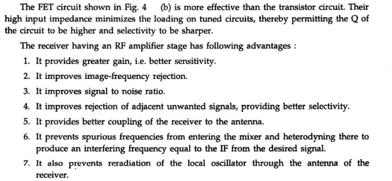
95 1. RF Amplifier:


96 2. Mixer Separately Excited Mixer: Fig.5 Separately Excited FET Mixer


97 Self Excited Mixer: Fig.6. Self Excited Mixer 3. Tracking


98 4. Local Oscillator 5. IF Amplifier Fig.7 Two Stage IF Amplifier


99 Choice of Intermediate Frequency: 6. Automatic Gain Control Fig.8. Simple AGC circuit


100 Fig.9. Delayed AGC circuit Fig.10. Response of receiver with various AGC circuits.

101 FM Receiver: Fig.11. FM Receiver Block diagram


102 Comparisons with AM Receivers


103 Amplitude Limiter:


104
105
106 PULSE MODULATION Introduction: Pulse Modulation Carrier is a train of pulses Example: Pulse Amplitude Modulation (PAM), Pulse width modulation (PWM), Pulse Position Modulation (PPM) Types of Pulse Modulation: The immediate result of sampling is a pulse-amplitude modulation (PAM) signal PAM is an analog scheme in which the amplitude of the pulse is proportional to the amplitude of the signal at the instant of sampling Another analog pulse-forming technique is known as pulse-duration modulation (PDM). This is also known as pulse-width modulation (PWM) Pulse-position modulation is closely related to PDM Pulse Amplitude Modulation: In PAM, amplitude of pulses is varied in accordance with instantaneous value of modulating signal. PAM Generation: The carrier is in the form of narrow pulses having frequency fc. The uniform sampling takes place in multiplier to generate PAM signal. Samples are placed Ts sec away from each other.
107 The circuit is simple emitter follower. Fig.12. PAM Modulator In the absence of the clock signal, the output follows input. The modulating signal is applied as the input signal. Another input to the base of the transistor is the clock signal. The frequency of the clock signal is made equal to the desired carrier pulse train frequency. The amplitude of the clock signal is chosen the high level is at ground level(0v) and low level at some negative voltage sufficient to bring the transistor in cutoff region. When clock is high, circuit operates as emitter follower and the output follows in the input modulating signal. When clock signal is low, transistor is cutoff and output is zero. Thus the output is the desired PAM signal. PAM Demodulator: The PAM demodulator circuit which is just an envelope detector followed by a second order op-amp low pass filter (to have good filtering characteristics) is as shown below Fig.13. PAM Demodulator

108 Pulse Width Modulation: In this type, the amplitude is maintained constant but the width of each pulse is varied in accordance with instantaneous value of the analog signal. In PWM information is contained in width variation. This is similar to FM. In pulse width modulation (PWM), the width of each pulse is made directly proportional to the amplitude of the information signal. Pulse Position Modulation: In this type, the sampled waveform has fixed amplitude and width whereas the position of each pulse is varied as per instantaneous value of the analog signal. PPM signal is further modification of a PWM signal. PPM & PWM Modulator: Fig.14. PWM & PPM Modulator The PPM signal can be generated from PWM signal. The PWM pulses obtained at the comparator output are applied to a mono stable multi vibrator which is negative edge triggered.
Speech, music, images, and video are examples of analog signals. Each of these signals is characterized by its bandwidth, dynamic range, and the
 Speech, music, images, and video are examples of analog signals. Each of these signals is characterized by its bandwidth, dynamic range, and the nature of the signal. For instance, in the case of audio
B.Tech II Year II Semester (R13) Supplementary Examinations May/June 2017 ANALOG COMMUNICATION SYSTEMS (Electronics and Communication Engineering)
 Supplementary Examinations May/June 2017 ANALOG COMMUNICATION SYSTEMS (Electronics and Communication Engineering)") Code: 13A04404 R13 B.Tech II Year II Semester (R13) Supplementary Examinations May/June 2017 ANALOG COMMUNICATION SYSTEMS (Electronics and Communication Engineering) Time: 3 hours Max. Marks: 70 PART A
Code: 13A04404 R13 B.Tech II Year II Semester (R13) Supplementary Examinations May/June 2017 ANALOG COMMUNICATION SYSTEMS (Electronics and Communication Engineering) Time: 3 hours Max. Marks: 70 PART A
Outline. Communications Engineering 1
 Outline Introduction Signal, random variable, random process and spectra Analog modulation Analog to digital conversion Digital transmission through baseband channels Signal space representation Optimal
Lecture 6. Angle Modulation and Demodulation
 Lecture 6 and Demodulation Agenda Introduction to and Demodulation Frequency and Phase Modulation Angle Demodulation FM Applications Introduction The other two parameters (frequency and phase) of the carrier
UNIT I AMPLITUDE MODULATION
 UNIT I AMPLITUDE MODULATION Prepared by: S.NANDHINI, Assistant Professor, Dept. of ECE, Sri Venkateswara College of Engineering, Sriperumbudur, Tamilnadu. CONTENTS Introduction to communication systems
Amplitude Modulated Systems
 Amplitude Modulated Systems Communication is process of establishing connection between two points for information exchange. Channel refers to medium through which message travels e.g. wires, links, or
Amplitude Modulation II
 Lecture 6: Amplitude Modulation II EE 3770: Communication Systems Lecture 6 Amplitude Modulation II AM Limitations DSB-SC Modulation SSB Modulation VSB Modulation Multiplexing Mojtaba Vaezi 6-1 Contents
UNIT-I AMPLITUDE MODULATION (2 Marks Questions and Answers)
") UNIT-I AMPLITUDE MODULATION (2 Marks Questions and Answers) 1. Define modulation? Modulation is a process by which some characteristics of high frequency carrier Signal is varied in accordance with the
UNIT-I AMPLITUDE MODULATION (2 Marks Questions and Answers) 1. Define modulation? Modulation is a process by which some characteristics of high frequency carrier Signal is varied in accordance with the
AM Limitations. Amplitude Modulation II. DSB-SC Modulation. AM Modifications
 Lecture 6: Amplitude Modulation II EE 3770: Communication Systems AM Limitations AM Limitations DSB-SC Modulation SSB Modulation VSB Modulation Lecture 6 Amplitude Modulation II Amplitude modulation is
(b) What are the differences between FM and PM? (c) What are the differences between NBFM and WBFM? [9+4+3]
![(b) What are the differences between FM and PM? (c) What are the differences between NBFM and WBFM? [9+4+3]](/thumbs/85/91561193.jpg "(b) What are the differences between FM and PM? (c) What are the differences between NBFM and WBFM? [9+4+3]") Code No: RR220401 Set No. 1 1. (a) The antenna current of an AM Broadcast transmitter is 10A, if modulated to a depth of 50% by an audio sine wave. It increases to 12A as a result of simultaneous modulation
Code No: RR220401 Set No. 1 1. (a) The antenna current of an AM Broadcast transmitter is 10A, if modulated to a depth of 50% by an audio sine wave. It increases to 12A as a result of simultaneous modulation
Charan Langton, Editor
 Charan Langton, Editor SIGNAL PROCESSING & SIMULATION NEWSLETTER Baseband, Passband Signals and Amplitude Modulation The most salient feature of information signals is that they are generally low frequency.
Code No: R Set No. 1
 Code No: R05220405 Set No. 1 II B.Tech II Semester Regular Examinations, Apr/May 2007 ANALOG COMMUNICATIONS ( Common to Electronics & Communication Engineering and Electronics & Telematics) Time: 3 hours
Master Degree in Electronic Engineering
 Master Degree in Electronic Engineering Analog and telecommunication electronic course (ATLCE-01NWM) Miniproject: Baseband signal transmission techniques Name: LI. XINRUI E-mail: s219989@studenti.polito.it
Communication Channels
 Communication Channels wires (PCB trace or conductor on IC) optical fiber (attenuation 4dB/km) broadcast TV (50 kw transmit) voice telephone line (under -9 dbm or 110 µw) walkie-talkie: 500 mw, 467 MHz
CHAPTER 2! AMPLITUDE MODULATION (AM)
") CHAPTER 2 AMPLITUDE MODULATION (AM) Topics 2-1 : AM Concepts 2-2 : Modulation Index and Percentage of Modulation 2-3 : Sidebands and the Frequency Domain 2-4 : Single-Sideband Modulation 2-5 : AM Power
CHAPTER 2 AMPLITUDE MODULATION (AM) Topics 2-1 : AM Concepts 2-2 : Modulation Index and Percentage of Modulation 2-3 : Sidebands and the Frequency Domain 2-4 : Single-Sideband Modulation 2-5 : AM Power
UNIT-2 Angle Modulation System
 UNIT-2 Angle Modulation System Introduction There are three parameters of a carrier that may carry information: Amplitude Frequency Phase Frequency Modulation Power in an FM signal does not vary with modulation
EXPERIMENT WISE VIVA QUESTIONS
 EXPERIMENT WISE VIVA QUESTIONS Pulse Code Modulation: 1. Draw the block diagram of basic digital communication system. How it is different from analog communication system. 2. What are the advantages of
Angle Modulated Systems
 Angle Modulated Systems Angle of carrier signal is changed in accordance with instantaneous amplitude of modulating signal. Two types Frequency Modulation (FM) Phase Modulation (PM) Use Commercial radio
Analog Communication.
 Analog Communication Vishnu N V Tele is Greek for at a distance, and Communicare is latin for to make common. Telecommunication is the process of long distance communications. Early telecommunications
Amplitude Modulation, II
 Amplitude Modulation, II Single sideband modulation (SSB) Vestigial sideband modulation (VSB) VSB spectrum Modulator and demodulator NTSC TV signsals Quadrature modulation Spectral efficiency Modulator
3.1 Introduction 3.2 Amplitude Modulation 3.3 Double Sideband-Suppressed Carrier Modulation 3.4 Quadrature-Carrier Multiplexing 3.
 Chapter 3 Amplitude Modulation Wireless Information Transmission System Lab. Institute of Communications Engineering g National Sun Yat-sen University Outline 3.1 Introduction 3. Amplitude Modulation 3.3
Communications and Signals Processing
 Communications and Signals Processing Department of Communications An Najah National University 2012/2013 1 3.1 Amplitude Modulation 3.2 Virtues, Limitations, and Modifications of Amplitude Modulation
3.1 Introduction to Modulation
 Haberlesme Sistemlerine Giris (ELE 361) 9 Eylul 2017 TOBB Ekonomi ve Teknoloji Universitesi, Guz 2017-18 Dr. A. Melda Yuksel Turgut & Tolga Girici Lecture Notes Chapter 3 Amplitude Modulation Speech, music,
S.E. (Electronics/Electronics and Telecommunication Engg.) (Second Semester) EXAMINATION, 2014 COMMUNICATION THEORY (2008 PATTERN)
 (Second Semester) EXAMINATION, 2014 COMMUNICATION THEORY (2008 PATTERN)") Total No. of Questions 12] [Total No. of Printed Pages 7 Seat No. [4657]-49 S.E. (Electronics/Electronics and Telecommunication Engg.) (Second Semester) EXAMINATION, 2014 COMMUNICATION THEORY (2008 PATTERN)
Total No. of Questions 12] [Total No. of Printed Pages 7 Seat No. [4657]-49 S.E. (Electronics/Electronics and Telecommunication Engg.) (Second Semester) EXAMINATION, 2014 COMMUNICATION THEORY (2008 PATTERN)
Lecture-3 Amplitude Modulation: Single Side Band (SSB) Modulation
 Modulation") Lecture-3 Amplitude Modulation: Single Side Band (SSB) Modulation 3.0 Introduction. 3.1 Baseband Signal SSB Modulation. 3.1.1 Frequency Domain Description. 3.1. Time Domain Description. 3. Single Tone
Lecture-3 Amplitude Modulation: Single Side Band (SSB) Modulation 3.0 Introduction. 3.1 Baseband Signal SSB Modulation. 3.1.1 Frequency Domain Description. 3.1. Time Domain Description. 3. Single Tone
4.1 REPRESENTATION OF FM AND PM SIGNALS An angle-modulated signal generally can be written as
 1 In frequency-modulation (FM) systems, the frequency of the carrier f c is changed by the message signal; in phase modulation (PM) systems, the phase of the carrier is changed according to the variations
ELEC 350 Communications Theory and Systems: I. Review. ELEC 350 Fall
 ELEC 350 Communications Theory and Systems: I Review ELEC 350 Fall 007 1 Final Examination Saturday, December 15-3 hours Two pages of notes allowed Calculator Tables provided Fourier transforms Table.1
Communication Engineering Prof. Surendra Prasad Department of Electrical Engineering Indian Institute of Technology, Delhi
 Communication Engineering Prof. Surendra Prasad Department of Electrical Engineering Indian Institute of Technology, Delhi Lecture - 10 Single Sideband Modulation We will discuss, now we will continue
Data Conversion Circuits & Modulation Techniques. Subhasish Chandra Assistant Professor Department of Physics Institute of Forensic Science, Nagpur
 Data Conversion Circuits & Modulation Techniques Subhasish Chandra Assistant Professor Department of Physics Institute of Forensic Science, Nagpur Data Conversion Circuits 2 Digital systems are being used
Signals and Systems Lecture 9 Communication Systems Frequency-Division Multiplexing and Frequency Modulation (FM)
") Signals and Systems Lecture 9 Communication Systems Frequency-Division Multiplexing and Frequency Modulation (FM) April 11, 2008 Today s Topics 1. Frequency-division multiplexing 2. Frequency modulation
Signals and Systems Lecture 9 Communication Systems Frequency-Division Multiplexing and Frequency Modulation (FM) April 11, 2008 Today s Topics 1. Frequency-division multiplexing 2. Frequency modulation
 UNIT I FUNDAMENTALS OF ANALOG COMMUNICATION Introduction In the Microbroadcasting services, a reliable radio communication system is of vital importance. The swiftly moving operations of modern communities
ELEC3242 Communications Engineering Laboratory Amplitude Modulation (AM)
") ELEC3242 Communications Engineering Laboratory 1 ---- Amplitude Modulation (AM) 1. Objectives 1.1 Through this the laboratory experiment, you will investigate demodulation of an amplitude modulated (AM)
ELEC3242 Communications Engineering Laboratory 1 ---- Amplitude Modulation (AM) 1. Objectives 1.1 Through this the laboratory experiment, you will investigate demodulation of an amplitude modulated (AM)
Amplitude Modulation. Ahmad Bilal
 Amplitude Modulation Ahmad Bilal 5-2 ANALOG AND DIGITAL Analog-to-analog conversion is the representation of analog information by an analog signal. Topics discussed in this section: Amplitude Modulation
DIGITAL COMMUNICATIONS SYSTEMS. MSc in Electronic Technologies and Communications
 DIGITAL COMMUNICATIONS SYSTEMS MSc in Electronic Technologies and Communications Bandpass binary signalling The common techniques of bandpass binary signalling are: - On-off keying (OOK), also known as
COMMUNICATION SYSTEMS
 COMMUNICATION SYSTEMS 1. A cordless telephone using separate frequencies for transmission in base and portable units is known as A. duplex arrangement B. half duplex arrangement C. either (a) or (b) D.
Introduction to Amplitude Modulation
 1 Introduction to Amplitude Modulation Introduction to project management. Problem definition. Design principles and practices. Implementation techniques including circuit design, software design, solid
Wireless Communication Fading Modulation
 EC744 Wireless Communication Fall 2008 Mohamed Essam Khedr Department of Electronics and Communications Wireless Communication Fading Modulation Syllabus Tentatively Week 1 Week 2 Week 3 Week 4 Week 5
Chapter 3. Amplitude Modulation Fundamentals
 Chapter 3 Amplitude Modulation Fundamentals Topics Covered 3-1: AM Concepts 3-2: Modulation Index and Percentage of Modulation 3-3: Sidebands and the Frequency Domain 3-4: AM Power 3-5: Single-Sideband
Modulation Methods Frequency Modulation
 Modulation Methods Frequency Modulation William Sheets K2MQJ Rudolf F. Graf KA2CWL The use of frequency modulation (called FM) is another method of adding intelligence to a carrier signal. While simple
ELEC3242 Communications Engineering Laboratory Frequency Shift Keying (FSK)
") ELEC3242 Communications Engineering Laboratory 1 ---- Frequency Shift Keying (FSK) 1) Frequency Shift Keying Objectives To appreciate the principle of frequency shift keying and its relationship to analogue
ELEC3242 Communications Engineering Laboratory 1 ---- Frequency Shift Keying (FSK) 1) Frequency Shift Keying Objectives To appreciate the principle of frequency shift keying and its relationship to analogue
Internal Examination I Answer Key DEPARTMENT OF CSE & IT. Semester: III Max.Marks: 100
 NH 67, Karur Trichy Highways, Puliyur C.F, 639 114 Karur District Internal Examination I Answer Key DEPARTMENT OF CSE & IT Branch & Section: II CSE & IT Date & Time: 06.08.15 & 3 Hours Semester: III Max.Marks:
VALLIAMMAI ENGINEERING COLLEGE
 VALLIAMMAI ENGINEERING COLLEGE SRM Nagar, Kattankulathur 603 203. DEPARTMENT OF ELECTRONICS & COMMUNICATION ENGINEERING QUESTION BANK SUBJECT : EC6402 COMMUNICATION THEORY SEM / YEAR: IV / II year B.E.
EC2252: COMMUNICATION THEORY SEM / YEAR: II year DEPARTMENT OF ELECTRONICS AND COMMUNICATION ENGINEERING
 EC2252: COMMUNICATION THEORY SEM / YEAR: II year DEPARTMENT OF ELECTRONICS AND COMMUNICATION ENGINEERING QUESTION BANK SUBJECT CODE : EC2252 SEM / YEAR : II year SUBJECT NAME : COMMUNICATION THEORY UNIT
Part A: Question & Answers UNIT I AMPLITUDE MODULATION
 PANDIAN SARASWATHI YADAV ENGINEERING COLLEGE DEPARTMENT OF ELECTRONICS & COMMUNICATON ENGG. Branch: ECE EC6402 COMMUNICATION THEORY Semester: IV Part A: Question & Answers UNIT I AMPLITUDE MODULATION 1.
Amplitude Modulation Chapter 2. Modulation process
 Question 1 Modulation process Modulation is the process of translation the baseband message signal to bandpass (modulated carrier) signal at frequencies that are very high compared to the baseband frequencies.
COMM 601: Modulation I
 Prof. Ahmed El-Mahdy, Communications Department The German University in Cairo Text Books [1] Couch, Digital and Analog Communication Systems, 7 th edition, Prentice Hall, 2007. [2] Simon Haykin, Communication
Amplitude Modulation Fundamentals
 3 chapter Amplitude Modulation Fundamentals In the modulation process, the baseband voice, video, or digital signal modifies another, higher-frequency signal called the carrier, which is usually a sine
Elements of Communication System Channel Fig: 1: Block Diagram of Communication System Terminology in Communication System
 Content:- Fundamentals of Communication Engineering : Elements of a Communication System, Need of modulation, electromagnetic spectrum and typical applications, Unit V (Communication terminologies in communication
 Modulations Analog Modulations Amplitude modulation (AM) Linear modulation Frequency modulation (FM) Phase modulation (PM) cos Angle modulation FM PM Digital Modulations ASK FSK PSK MSK MFSK QAM PAM Etc.
4- Single Side Band (SSB)
") 4- Single Side Band (SSB) It can be shown that: s(t) S.S.B = m(t) cos ω c t ± m h (t) sin ω c t -: USB ; +: LSB m(t) X m(t) cos ω c t -π/ cos ω c t -π/ + s S.S.B m h (t) X m h (t) ± sin ω c t 1 Tone Modulation:
4- Single Side Band (SSB) It can be shown that: s(t) S.S.B = m(t) cos ω c t ± m h (t) sin ω c t -: USB ; +: LSB m(t) X m(t) cos ω c t -π/ cos ω c t -π/ + s S.S.B m h (t) X m h (t) ± sin ω c t 1 Tone Modulation:
PRODUCT DEMODULATION - SYNCHRONOUS & ASYNCHRONOUS
 PRODUCT DEMODULATION - SYNCHRONOUS & ASYNCHRONOUS INTRODUCTION...98 frequency translation...98 the process...98 interpretation...99 the demodulator...100 synchronous operation: ω 0 = ω 1...100 carrier
ELE636 Communication Systems
 ELE636 Communication Systems Chapter 5 : Angle (Exponential) Modulation 1 Phase-locked Loop (PLL) The PLL can be used to track the phase and the frequency of the carrier component of an incoming signal.
Problems from the 3 rd edition
 (2.1-1) Find the energies of the signals: a) sin t, 0 t π b) sin t, 0 t π c) 2 sin t, 0 t π d) sin (t-2π), 2π t 4π Problems from the 3 rd edition Comment on the effect on energy of sign change, time shifting
EE390 Final Exam Fall Term 2002 Friday, December 13, 2002
 Name Page 1 of 11 EE390 Final Exam Fall Term 2002 Friday, December 13, 2002 Notes 1. This is a 2 hour exam, starting at 9:00 am and ending at 11:00 am. The exam is worth a total of 50 marks, broken down
15.Calculate the local oscillator frequency if incoming frequency is F1 and translated carrier frequency
 DEPARTMENT OF ELECTRONICS & COMMUNICATION ENGINEERING SUBJECT NAME:COMMUNICATION THEORY YEAR/SEM: II/IV SUBJECT CODE: EC 6402 UNIT I:l (AMPLITUDE MODULATION) PART A 1. Compute the bandwidth of the AMP
Angle Modulation, II. Lecture topics. FM bandwidth and Carson s rule. Spectral analysis of FM. Narrowband FM Modulation. Wideband FM Modulation
 Angle Modulation, II Lecture topics FM bandwidth and Carson s rule Spectral analysis of FM Narrowband FM Modulation Wideband FM Modulation Bandwidth of Angle-Modulated Waves Angle modulation is nonlinear
1B Paper 6: Communications Handout 2: Analogue Modulation
 1B Paper 6: Communications Handout : Analogue Modulation Ramji Venkataramanan Signal Processing and Communications Lab Department of Engineering ramji.v@eng.cam.ac.uk Lent Term 16 1 / 3 Modulation Modulation
ECE5713 : Advanced Digital Communications
 ECE5713 : Advanced Digital Communications Bandpass Modulation MPSK MASK, OOK MFSK 04-May-15 Advanced Digital Communications, Spring-2015, Week-8 1 In-phase and Quadrature (I&Q) Representation Any bandpass
Communications I (ELCN 306)
") Communications I (ELCN 306) c Samy S. Soliman Electronics and Electrical Communications Engineering Department Cairo University, Egypt Email: samy.soliman@cu.edu.eg Website: http://scholar.cu.edu.eg/samysoliman
Communications I (ELCN 306) c Samy S. Soliman Electronics and Electrical Communications Engineering Department Cairo University, Egypt Email: samy.soliman@cu.edu.eg Website: http://scholar.cu.edu.eg/samysoliman
Modulation is the process of impressing a low-frequency information signal (baseband signal) onto a higher frequency carrier signal
 onto a higher frequency carrier signal") Modulation is the process of impressing a low-frequency information signal (baseband signal) onto a higher frequency carrier signal Modulation is a process of mixing a signal with a sinusoid to produce
Modulation is the process of impressing a low-frequency information signal (baseband signal) onto a higher frequency carrier signal Modulation is a process of mixing a signal with a sinusoid to produce
AM, PM and FM mo m dula l ti t o i n
 AM, PM and FM modulation What is amplitude modulation In order that a radio signal can carry audio or other information for broadcasting or for two way radio communication, it must be modulated or changed
(Refer Slide Time: 3:11)
") Digital Communication. Professor Surendra Prasad. Department of Electrical Engineering. Indian Institute of Technology, Delhi. Lecture-2. Digital Representation of Analog Signals: Delta Modulation. Professor:
Digital Communication. Professor Surendra Prasad. Department of Electrical Engineering. Indian Institute of Technology, Delhi. Lecture-2. Digital Representation of Analog Signals: Delta Modulation. Professor:
Q.P. Code : [ TURN OVER]
![Q.P. Code : [ TURN OVER]](/thumbs/90/103239233.jpg "Q.P. Code : [ TURN OVER]") Q.P. Code : 587801 8ADF85B2CAF8DDC703193679392A86308ADF85B2CAF8DDC703193679392A86308ADF85B2CAF8DDC703193679392A86308ADF85B2CAF8DDC703193679392A86308ADF85B2CAF8DDC70 6308ADF85B2CAF8DDC703193679392A86308ADF85B2CAF8DDC703193679392A86308ADF85B2CAF8DDC703193679392A86308ADF85B2CAF8DDC703193679392A86308ADF85B2CAF8DDC703
Q.P. Code : 587801 8ADF85B2CAF8DDC703193679392A86308ADF85B2CAF8DDC703193679392A86308ADF85B2CAF8DDC703193679392A86308ADF85B2CAF8DDC703193679392A86308ADF85B2CAF8DDC70 6308ADF85B2CAF8DDC703193679392A86308ADF85B2CAF8DDC703193679392A86308ADF85B2CAF8DDC703193679392A86308ADF85B2CAF8DDC703193679392A86308ADF85B2CAF8DDC703
Chapter 3: Analog Modulation Cengage Learning Engineering. All Rights Reserved.
 Contemporary Communication Systems using MATLAB Chapter 3: Analog Modulation 2013 Cengage Learning Engineering. All Rights Reserved. 3.1 Preview In this chapter we study analog modulation & demodulation,
Part-I. Experiment 6:-Angle Modulation
 Part-I Experiment 6:-Angle Modulation 1. Introduction 1.1 Objective This experiment deals with the basic performance of Angle Modulation - Phase Modulation (PM) and Frequency Modulation (FM). The student
EEE 309 Communication Theory
 EEE 309 Communication Theory Semester: January 2017 Dr. Md. Farhad Hossain Associate Professor Department of EEE, BUET Email: mfarhadhossain@eee.buet.ac.bd Office: ECE 331, ECE Building Types of Modulation
Introduction. Amplitude Modulation System Angle Modulation System
 Introduction Amplitude Modulation System Angle Modulation System Frequency Modulation Phase Modulation Digital Communication Elements of Information Theory Advanced Communication Techniques 1 Tools for
Pulse-Width Modulation (PWM)
") Pulse-Width Modulation (PWM) Modules: Integrate & Dump, Digital Utilities, Wideband True RMS Meter, Tuneable LPF, Audio Oscillator, Multiplier, Utilities, Noise Generator, Speech, Headphones. 0 Pre-Laboratory
Pulse-Width Modulation (PWM) Modules: Integrate & Dump, Digital Utilities, Wideband True RMS Meter, Tuneable LPF, Audio Oscillator, Multiplier, Utilities, Noise Generator, Speech, Headphones. 0 Pre-Laboratory
Amplitude Modulation Early Radio EE 442 Spring Semester Lecture 6
 Amplitude Modulation Early Radio EE 442 Spring Semester Lecture 6 f f f LO audio baseband m http://www.technologyuk.net/telecommunications/telecom_principles/amplitude_modulation.shtml AM Modulation --
ANALOGUE TRANSMISSION OVER FADING CHANNELS
 J.P. Linnartz EECS 290i handouts Spring 1993 ANALOGUE TRANSMISSION OVER FADING CHANNELS Amplitude modulation Various methods exist to transmit a baseband message m(t) using an RF carrier signal c(t) =
DT Filters 2/19. Atousa Hajshirmohammadi, SFU
 1/19 ENSC380 Lecture 23 Objectives: Signals and Systems Fourier Analysis: Discrete Time Filters Analog Communication Systems Double Sideband, Sub-pressed Carrier Modulation (DSBSC) Amplitude Modulation
EE3723 : Digital Communications
 EE3723 : Digital Communications Week 8-9: Bandpass Modulation MPSK MASK, OOK MFSK 04-May-15 Muhammad Ali Jinnah University, Islamabad - Digital Communications - EE3723 1 In-phase and Quadrature (I&Q) Representation
! Amplitude of carrier wave varies a mean value in step with the baseband signal m(t)
") page 7.1 CHAPTER 7 AMPLITUDE MODULATION Transmit information-bearing (message) or baseband signal (voice-music) through a Communications Channel Baseband = band of frequencies representing the original
page 7.1 CHAPTER 7 AMPLITUDE MODULATION Transmit information-bearing (message) or baseband signal (voice-music) through a Communications Channel Baseband = band of frequencies representing the original
 DEPARTMENT OF COMPUTER GCE@Bodi_ SCIENCE GCE@Bodi_ AND ENIGNEERING GCE@Bodi_ GCE@Bodi_ GCE@Bodi_ Analog and Digital Communication GCE@Bodi_ DEPARTMENT OF CsE Subject Name: Analog and Digital Communication
 VALLIAMMAI ENGINEERING COLLEGE SRM Nagar, Kattankulathur 603 203. DEPARTMENT OF ELECTRONICS & COMMUNICATION ENGINEERING QUESTION BANK EC6402 COMMUNICATION THEORY III YEAR / VI SEMESTER ACADEMIC YEAR 2015-16(EVEN)
Outline. Communications Engineering 1
 Outline Introduction Signal, random variable, random process and spectra Analog modulation Analog to digital conversion Digital transmission through baseband channels Signal space representation Optimal
S.R.M. Institute of Science & Technology School of Electronics & Communication Engineering
 S.R.M. Institute of Science & Technology School of Electronics & Communication Engineering QUESTION BANK Subject Code : EC314 Subject Name : Communication Engineering Year & Sem : III Year, 6th Sem (EEE)
AN INTRODUCTION OF ANALOG AND DIGITAL MODULATION TECHNIQUES IN COMMUNICATION SYSTEM
 AN INTRODUCTION OF ANALOG AND DIGITAL MODULATION TECHNIQUES IN COMMUNICATION SYSTEM Rashmi Pandey Vedica Institute of Technology, Bhopal Department of Electronics & Communication rashmipandey07@rediffmail.com
OBJECTIVES EQUIPMENT LIST
 1 Reception of Amplitude Modulated Signals AM Demodulation OBJECTIVES The purpose of this experiment is to show how the amplitude-modulated signals are demodulated to obtain the original signal. Also,
Laboratory Assignment 5 Amplitude Modulation
 Laboratory Assignment 5 Amplitude Modulation PURPOSE In this assignment, you will explore the use of digital computers for the analysis, design, synthesis, and simulation of an amplitude modulation (AM)
ANALOG COMMUNICATION
 ANALOG COMMUNICATION TRAINING LAB Analog Communication Training Lab consists of six kits, one each for Modulation (ACL-01), Demodulation (ACL-02), Modulation (ACL-03), Demodulation (ACL-04), Noise power
V. CHANDRA SEKAR Professor and Head Department of Electronics and Communication Engineering SASTRA University, Kumbakonam
 V. CHANDRA SEKAR Professor and Head Department of Electronics and Communication Engineering SASTRA University, Kumbakonam 1 Contents Preface v 1. Introduction 1 1.1 What is Communication? 1 1.2 Modulation
Chapter 5. Amplitude Modulation
 Chapter 5 Amplitude Modulation So far we have developed basic signal and system representation techniques which we will now apply to the analysis of various analog communication systems. In particular,
EE4512 Analog and Digital Communications Chapter 6. Chapter 6 Analog Modulation and Demodulation
 Chapter 6 Analog Modulation and Demodulation Chapter 6 Analog Modulation and Demodulation Amplitude Modulation Pages 306-309 309 The analytical signal for double sideband, large carrier amplitude modulation
Description of the AM Superheterodyne Radio Receiver
 Superheterodyne AM Radio Receiver Since the inception of the AM radio, it spread widely due to its ease of use and more importantly, it low cost. The low cost of most AM radios sold in the market is due
RF/IF Terminology and Specs
 RF/IF Terminology and Specs Contributors: Brad Brannon John Greichen Leo McHugh Eamon Nash Eberhard Brunner 1 Terminology LNA - Low-Noise Amplifier. A specialized amplifier to boost the very small received
Electronics Interview Questions
 Electronics Interview Questions 1. What is Electronic? The study and use of electrical devices that operate by controlling the flow of electrons or other electrically charged particles. 2. What is communication?
ECE513 RF Design for Wireless
 1 ECE513 RF Design for Wireless MODULE 1 RF Systems LECTURE 1 Modulation Techniques Chapter 1, Sections 1.1 1.3 Professor Michael Steer http://www4.ncsu.edu/~mbs 2 Module 1: RF Systems Amplifiers, Mixers
Keywords Internet, LabVIEW, Smart Classroom-cum-Laboratory, Teaching and Learning process of communication.
 Volume 4, Issue 10, October 2014 ISSN: 2277 128X International Journal of Advanced Research in Computer Science and Software Engineering Research Paper Available online at: www.ijarcsse.com Smart Classroom-cum-Laboratory
EXAMINATION FOR THE DEGREE OF B.E. Semester 1 June COMMUNICATIONS IV (ELEC ENG 4035)
") EXAMINATION FOR THE DEGREE OF B.E. Semester 1 June 2007 101902 COMMUNICATIONS IV (ELEC ENG 4035) Official Reading Time: Writing Time: Total Duration: 10 mins 120 mins 130 mins Instructions: This is a closed
EXAMINATION FOR THE DEGREE OF B.E. Semester 1 June 2007 101902 COMMUNICATIONS IV (ELEC ENG 4035) Official Reading Time: Writing Time: Total Duration: 10 mins 120 mins 130 mins Instructions: This is a closed
EE 400L Communications. Laboratory Exercise #7 Digital Modulation
 EE 400L Communications Laboratory Exercise #7 Digital Modulation Department of Electrical and Computer Engineering University of Nevada, at Las Vegas PREPARATION 1- ASK Amplitude shift keying - ASK - in
UNIT 1 QUESTIONS WITH ANSWERS
 UNIT 1 QUESTIONS WITH ANSWERS 1. Define modulation? Modulation is a process by which some characteristics of high frequency carrier signal is varied in accordance with the instantaneous value of the modulating
EE470 Electronic Communication Theory Exam II
 EE470 Electronic Communication Theory Exam II Open text, closed notes. For partial credit, you must show all formulas in symbolic form and you must work neatly!!! Date: November 6, 2013 Name: 1. [16%]
S.R.M Institute of Science and Technology (Deemed University) Department of Electronics & Communication Engineering
 Department of Electronics & Communication Engineering") S.R.M Institute of Science and Technology (Deemed University) Department of Electronics & Communication Engineering QUESTION BANK Subject Code : EC211 Subject Name : Communication Engineering Year & Sem
S.R.M Institute of Science and Technology (Deemed University) Department of Electronics & Communication Engineering QUESTION BANK Subject Code : EC211 Subject Name : Communication Engineering Year & Sem
EE 460L University of Nevada, Las Vegas ECE Department
 EE 460L PREPARATION 1- ASK Amplitude shift keying - ASK - in the context of digital communications is a modulation process which imparts to a sinusoid two or more discrete amplitude levels. These are related
PHASE DIVISION MULTIPLEX
 PHASE DIVISION MULTIPLEX PREPARATION... 70 the transmitter... 70 the receiver... 71 EXPERIMENT... 72 a single-channel receiver... 72 a two-channel receiver... 73 TUTORIAL QUESTIONS... 74 Vol A2, ch 8,
DEPARTMENT OF E.C.E.
 PVP SIDDHARTHA INSTITUTE OF TECHNOLOGY, KANURU, VIJAYAWADA-7 DEPARTMENT OF E.C.E. ANALOG COMMUNICATIONS LAB MANUAL Department of Electronics & Communication engineering Prasad V.Potluri Siddhartha Institute
ANALOG AND DIGITAL COMMUNICATION DATA AND PULSE COMMUNICATION HISTORY OF DATA COMMUNICATION, STANDARDS ORGANIZATIONS FOR DATA COMMUNICATION.
 UNIT III DATA AND PULSE COMMUNICATION 3.1 DATA COMMUNICATION: HISTORY OF DATA COMMUNICATION, STANDARDS ORGANIZATIONS FOR DATA COMMUNICATION. Data communication can be defined as two personal computers
two computers. 2- Providing a channel between them for transmitting and receiving the signals through it.
 1. Introduction: Communication is the process of transmitting the messages that carrying information, where the two computers can be communicated with each other if the two conditions are available: 1-
cosω t Y AD 532 Analog Multiplier Board EE18.xx Fig. 1 Amplitude modulation of a sine wave message signal
 University of Saskatchewan EE 9 Electrical Engineering Laboratory III Amplitude and Frequency Modulation Objectives: To observe the time domain waveforms and spectra of amplitude modulated (AM) waveforms