ELEC3242 Communications Engineering Laboratory Frequency Shift Keying (FSK)
|
|
|
- Hope McCoy
- 5 years ago
- Views:
Transcription
1 ELEC3242 Communications Engineering Laboratory Frequency Shift Keying (FSK) 1) Frequency Shift Keying Objectives To appreciate the principle of frequency shift keying and its relationship to analogue frequency modulation To generate a two-level (binary) frequency shift keyed signal and investigate the spectrum and bandwidth associated with it To investigate the demodulation of an FSK signal To understand the concept of Minimum shift keying and its use to limit the bandwidth of an FSK signal To generate and subsequently demodulate a minimum shift keyed signal To appreciate the concept of multi-level FSK (MFSK) and to generate 4, 8 and 16 level MFSK signals To investigate the spectrum occupied by an MFSK signal and its relationship to symbol rate 2) Bessel Function and FM Modulation The equation of a sinusoidal voltage waveform is given by: where: v is the instantaneous voltage, v = V max.sin(ωt+ø) V max is the maximum voltage amplitude, ω is the angular frequency, Ø is the phase.
2 A steady voltage corresponding to the above equation conveys little information. To convey information the waveform must be made to vary so that the variations represent the information. This process is called modulation. Any of these may be varied to convey information. Frequency Modulation Frequency modulation uses variations in frequency to convey information. The wave whose frequency is being varied is called the carrier wave. The signal doing the variation is called the modulating signal. For simplicity, suppose both carrier wave and modulating signal are sinusoidal; ie: (c denotes carrier) and (m denotes modulation) v c = V c sin ω c t v m = V m cos ω m t What is Frequency? If the frequency is varying, how can it be defined? You can no longer count the number of cycles over a longish interval to determine the cycles per second. Instead, frequency is defined as the rate of change of phase.
3 This is consistent with the simple definition because, at a constant (angular) frequency ω radians/second, the phase is changing at ω radians per second, which is ω/2π cycles per second. Since the instantaneous frequency can only be defined by reference to the phase, the phase must be examined in order to arrive at an expression for the frequency-modulated signal. Phase of the FM Signal For the unmodulated carrier v c = V c sin ω c t, the phase is: φ = ω c t The modulating signal varies the carrier frequency, ω c, so that its frequency takes the form: ω = ω c + D cos ω m t (where D denotes the peak value of the deviation). It is related to the amplitude of the modulating signal v m by the 'frequency slope' of the frequency modulator (VCO), say k radians/s per V. The peak value of v m produces deviation D, so: D = k V m The total phase change undergone at time t is found by integrating the angular frequency. It is φ = (ω c + D cos ω m t) dt = ω c t + (D/ω m ) sin ω m t (If you are not familiar with integration you will have to take this result on trust). So the FM signal can be expressed as: V c sin [ω c t + (D/ω m ) sin ω m t]
4 Modulation Index In the expression for the FM signal: V c sin [ω c t + (D/ω m ) sin ω m t] the coefficient D/ω m turns out to be quite important and is given the name modulation index. It is often represented by the Greek letter beta, β. So we may write the FM signal as: v c = V c sin (ω c t + βsin ω m ) t where β is the modulation index D/ω m. In this expression, the factor sin (ω c t + βsin ω m )t (let us call it F) is of the form sin(a + b), which can be expanded to sin a cos b + cos a sin b. Applying this expansion to F, we get: F = sin ω c t cos(sin βω m ) t + cos ω c t sin (sin βω m ) t FM Sidebands These complicated functions can be expanded, using mathematics too elaborate to explain here, into a series of terms like this: F = J 0 (β) sin ω c t+ J 1 (β) [ sin (ω c + ω m )t - sin (ω c - ω m )t ] + J 2 (β) [ sin (ω c + 2ω m )t - sin (ω c - 2ω m )t ] + J 3 (β) [ sin (ω c + 3ω m )t - sin (ω c - 3ω m )t ] + J 4 (β) [ sin (ω c + 4ω m )t - sin (ω c - 4ω m )t ] +... where J 0 (β), J 1 (β), J 2 (β) etc are constants whose values depend only on β. They are called Bessel Functions. There is an infinite series of these functions, and so an infinite number of FM sidebands. But, in practice the values of the Bessel functions become very small as the series goes on. For example, when β = 2

5 J 0 (2) = J 1 (2) = J 2 (2) = J 3 (2) = J 4 (2) = J 5 (2) = A Practical Approximate Rule Because the higher-order sidebands become very small, in practice the bandwidth of the FM signal may be restricted to a finite bandwidth. The practical rule that is used, often called Carson s Rule, is to take the bandwidth required as: B = 2 ( F d + F m ) where B is the bandwidth, F d the deviation and F m is the bandwidth of the modulation, all in the same units. 3) The Phase Locked Loop A phase locked loop (PLL) is a sub system that enables an oscillator to be synchronized in frequency and phase to an incoming signal. The block diagram shows the building blocks that make up a phase locked loop. Imagine that the voltage controlled oscillator (VCO) is oscillating near to the incoming signal frequency. The output of the phase/frequency comparator is a signal that represents the frequency error between the VCO and the incoming signal. This signal is applied to the frequency control input of the VCO, which then changes its frequency to be equal to the incoming signal. The output of the comparator then compares the phases of the two signals and uses the VCO frequency control to match the two phases. The system is now in lock. If either the signal or the VCO moves in phase with respect to each other the comparator output moves the VCO so that the two are always locked together. In fact most PLLs only use a phase comparator (detector). This is because phase detectors, when presented with two different frequencies, produce an ac signal equal in frequency to the difference between them. This has the effect of swinging the VCO up and
6 down in frequency and, as it passes the signal frequency, the loop locks. Loop Stability One of the problems that will almost certainly arise, unless steps are taken to stop it, is instability. The loop relies on the system operating with negative feedback, i.e. if the VCO moves, the polarity of the control signal brings it back. This is easily done when the system is operating at, or near to, dc. However, a problem arises if you consider the loop moving in response to a fast changing frequency. The control signal will contain an ac component. All systems are subject to delays and phase shifts, which become more significant at higher frequencies. Remembering that 180 degrees phase shift is equivalent to inverting a signal, inevitably there is going to be a frequency at which the phase shift round the loop is enough to cause the polarity to reverse and positive feedback will be applied. This results in the system oscillating back and forth at the frequency which produces the positive feedback. There is another subtle problem that results in the design of a PLL system being more difficult then you might imagine. Remember that we are using the frequency of an oscillator to control its phase. Now phase is the integral of frequency and so there is already a 90 degree shift caused by the VCO. This means that there only has to be another 90 degrees of phase shift before instability, not 180 as you might have thought.
7 The same problem occurs, for example, in a mechanical position control system that uses speed control, because position is the integral of speed. The phase lock loop is a control system and exactly the same mathematics can be used to describe a PLL as is used to describe a position control servo. Of course, instability can only occur if there is enough gain in the loop at the problem frequency. This is where the loop filter can solve the problem, as it reduces gain at higher frequencies while maintaining control over phase. There will be a frequency that the loop filter produces 90 degrees of phase shift, but the gain will be low and so instability will not arise. The critical frequency is when the overall loop gain is 1 and the overall added phase shift must be less than 90 degrees at this point. The amount by which it is less is called phase margin and, in practice, should be about 45 degrees for good stable performance. The design of the loop filter is not simple and has to be done knowing all the gains and phase shifts in the system. Many phase comparators produce a control signal that contains a significant amount of high frequency energy but this is not normally a problem as it is removed by the loop filter. In PLLs that use phase only comparators, the bandwidth of the loop filter also determines the range over which the loop will lock on, or capture, a signal as the comparator only generates an ac signal off lock. The range over which the loop will capture a signal is called its capture range. The range over which the loop will remain locked, once lock is achieved, is called the lock range. The time to achieve lock can be important and is referred to as lock time. Phase Comparator A number of circuits will operate as phase comparators or detectors. A multiplier is often used. If the two inputs of a multiplier are fed with two signals that are at the same frequency, but with different phases, the output will comprise a twice-frequency component and a dc component that represents the phase error. There are some important restrictions to this, in that it will only operate over 180 degrees and has zero output at 90 degrees, not zero. The graph shows the output voltage for such a detector plotted against input phase difference.
8 This shows that the output repeats for 180 to 360, albeit in the other polarity. This phase range problem is not significant as, in a properly operating loop, the gain is such that only a small error has to occur before the VCO is corrected. There are other types of comparator. The logic function exclusive OR is exactly the same in action as the multiplier and is often used in digital circuits. More complex digital circuits have advantages, such as: acting as frequency comparators as well as phase comparators; operating over 360 degrees; and having less ac signal component in the output. Most of these are based on circuits using D type flip-flops. These D type comparators have the disadvantage of making the loop much less tolerant of noise in the signal. They are used in applications such as frequency synthesizers, while the multipliers and OR gates are used in applications such as demodulators or carrier reference recovery. The design of PLLs is a complex compromise of performance parameters, the relative importance of each performance parameter depends, to a large extent, on the application. Applications Many phase lock loops are used to recover some sort of constant frequency component to provide a reference for a demodulator. Another very common application is in frequency synthesizers, where an oscillator is frequency divided to some low frequency and a PLL locks it to an external reference. By changing the divider ratio, different frequencies that are all multiples of the reference frequency can be generated or synthesised. The PLL can also be used to demodulate FM as, when locked to the FM signal, the VCO tracks the frequency modulation. Therefore the control signal to the VCO contains the modulation, plus a dc component. This dc component can easily be removed using a high pass filter. In this case the loop filter bandwidth must be high enough to pass the modulation or the VCO will not be able to follow and the loop will come out of lock. In most
9 cases the output is passed through a post detection filter, which will remove any remaining high frequency components but, because it is outside the loop, will not affect loop stability. 4) Inter-symbol Interference Inter-symbol interference is a particular type of distortion applicable to digital signals. It simply refers to the fact that the present symbol may be distorted by the values of the symbols on either side of it. For example, if a post detection filter had insufficient bandwidth and the signal did not have time to reach its maximum output during a 1 symbol, if the previous symbol was zero, then this would be regarded as inter-symbol interference. More subtle problems may occur if there are reflections in a cable, or on radio signals, causing energy from other symbol periods to arrive at the same time. All communication systems use filtering to maximize the signal-to-noise ratio or prevent other signals causing interference. Any filtering will cause some inter-symbol interference and it is necessary to find the right compromise between too little filtering and too much distortion. Some systems, such as GMSK (Gaussian Minimum Shift Keying), are designed to tolerate significant distortion, in order to reduce their occupied bandwidth. 5) Symbol Rate and Bit Rate The concepts of symbols, bits, symbol rate and bit rate are important terms in digital communications. The concept of a bit (a binary digit) should be familiar as a one or zero in a binary data stream. The bit rate is simply the rate at which the bits change. For example, imagine a system that digitized an audio signal at 32k samples per second, each sample being digitized at 256 possible levels. This means each sample is an 8 bit word. In order to send this stream over a simple link it would have to be turned into serial data. This means the serial data stream would run at 32k x 8 = 256k bits per second. This is the bit rate. In this example we are assuming that there is no extra data for synchronization or for error correction. These bits are then modulated onto the carrier in some form. In order to be modulated they have to be converted to change some parameter of the carrier: its amplitude, frequency or phase. In a simple system there would be only two states: off or on, one frequency or the other, one of two phases etc. These states are called symbols. In the simplest binary system there are only two symbols and each bit has two possible states so the bits are directly mapped to symbols. This means that the symbol rate is equal to the bit rate. There is no reason why there have to be only two possible carrier states. In an amplitude shift keying (ASK) system there could be more than two possible amplitude states, or in phase shift keying (PSK) system there could be other possible phases than zero and 180 degrees. If there you had a PSK system with four possible states then each transmitted data symbol can be decoded as being one of four states. Therefore, not one but two bits can be carried per symbol. Now, if the bit rate remains the same, we only need to transmit symbols at half the rate. In such a system the symbol
10 rate is half the bit rate. If there were 16 symbols available then 4 bits per symbol could be Carried and the symbol rate would be one quarter the bit rate. Such systems are called M-ary, where M is the number of possible symbols, sometimes referred to as the order of the modulation scheme. In such a system the bit rate (B) is: B = Slog 2 M where S is the symbol rate and M the number of possible symbols. To avoid confusion this bit rate is sometimes called the gross bit rate It is important to remember that it is the symbol rate that is the rate at which the carrier changes state. Therefore, it determines the occupied bandwidth. It is clear that for a given bandwidth, the higher the order of the modulation scheme the less bandwidth is used. However there is a penalty to be paid. When demodulated, the higher the order of the scheme the more likely there are to be errors. This is obvious because, for example, it is clearly easier to detect the difference between 0 and 180 degrees than zero, 90, 180, and 270. There is another compromise to be made if error correcting data is added in that, although adding extra data reduces the number of errors, the bit rate has to rise, with a consequential increase in occupied bandwidth and received noise.
11 In order to calculate the amount of useful data that can be transmitted through a digital system, first find the symbol rate. Then calculate the bit rate by using the number of bits per symbol. The useful data, sometimes referred to as the payload, can then be calculated by subtracting the extra data added for error correction, data identification and synchronisation. In a multiplexed system more than one data stream may be present and you may have to find out what proportion of the data stream is allocated to a particular set of data. In very complex systems this proportion may not even be constant!
12 6) Practical 1: Generating and Demodulating Frequency Shift Keying Objectives and Background Frequency shift keying (FSK) is the transmission of digital data using frequency modulation. The simplest form of digital data, a binary bit stream, only contains two levels and these would be directly mapped to two frequencies. This means that the carrier simply switches between two discrete frequencies. There are also systems that use multi-level digital signals in order to conserve bandwidth by increasing the symbol rate. One advantage of frequency shift keying is that there are no amplitude changes; it is the frequency that moves, therefore advancing or retarding the phase linearly during a bit period. A signal that has no changes in amplitude can be passed, without distortion, through amplifiers that have non linear amplitude characteristics. All amplifiers are slightly nonlinear and this can result in unwanted sidebands being produced and thus the occupied bandwidth increases. This is often referred to as spectrum re-growth. Frequency modulated signals, analogue or digital, can be passed without problems through amplifiers that are highly non-linear. The advantage of this is that amplifiers can be made very power efficient at the expense of linearity and this is important where heat dissipation or battery life is an issue. A VCO can be used to generate FSK by simply feeding the control input with two voltage levels, representing one and zero. The magnitude of the voltage change is the deviation, referred to in FSK as the frequency shift. The value of frequency shift can vary widely. It can be a few percent of the carrier frequency or a factor of two to one, depending on the application. The occupied bandwidth depends not only on the frequency shift but also, of course, on the rate at which the frequency is switched. This is the bandwidth of the keying signal. Carson s rule still applies, as FSK is simply FM with a square wave signal as the modulation. There is usually some effort made to limit the maximum rate of frequency shift by using a pre-modulation filter. This has to be wide enough not to introduce too much inter-symbol interference. FSK has been used from the early days of digital communication systems, when the most advanced technology was a radio link and a teleprinter. It is still widely used today in applications as diverse as radio systems and telephone modems. In this Practical you will generate FSK using a VCO modulated by a square wave signal that represents a bit stream. You will demodulate it using a PLL. The techniques are very similar to those used for analogue FM. The next Practical will address the concepts ofminimum shift keying and aggressive premodulation filtering, which together reduce bandwidth requirements.
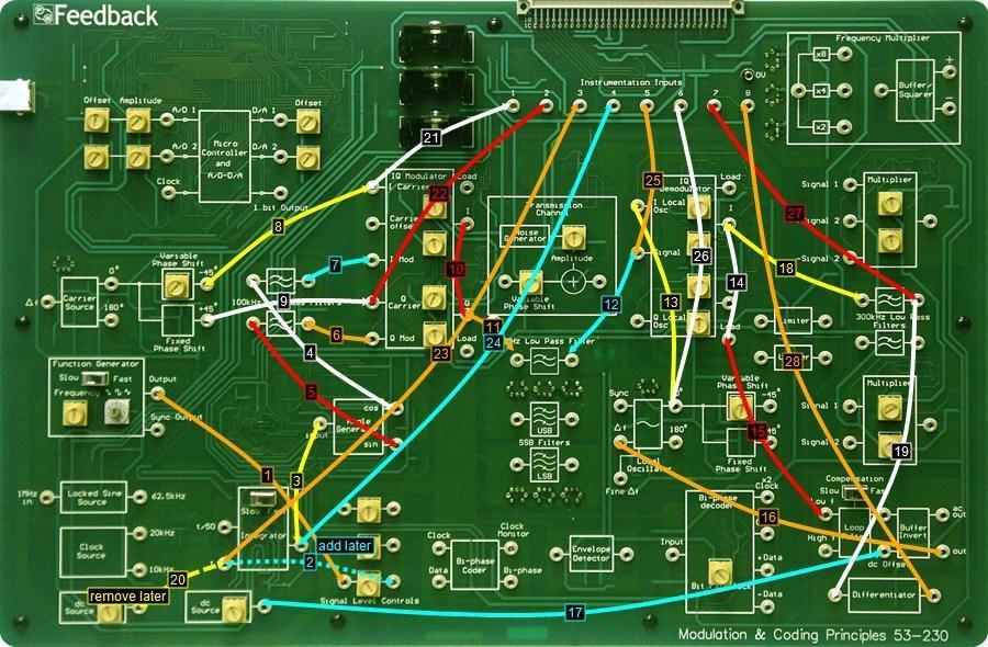
13 Block Diagram Make Connections Diagram
14 7) Practical 1: Generating and Demodulating Frequency Shift Keying Perform Practical Use the Make Connections diagram to show the required connections on the hardware. Initially you have connected up the circuit such that the Pre-modulation filter is not in circuit. Open the oscilloscope and the frequency counter. Set the Function Generator to Fast and select a square wave. Set the Signal Level Control to full scale to give maximum modulation. Set the IQ Demodulator controls to half scale. Set the Frequency of the Function Generator to about 7kHz. This is the frequency of the modulation. Note the data signal (square wave) on the lower oscilloscope trace and the upper trace (the carrier) showing no amplitude variation. Increase the oscilloscope time-base to maximum speed and use the x expand to see the individual cycles of the carrier. Change the trigger to Channel 1 by deselecting Y2 Trig. You should be able to see the carrier changing between two frequencies. Use the Defaults button to return the oscilloscope to the original settings. Open the spectrum analyser and note that the two possible frequencies for the carrier are clearly visible. Adjust the modulation amplitude using the Signal Level Control and note how the frequency shift changes. Use the Function Generator Frequency control to increase the frequency of the data (modulating) signal to about 40kHz. Note that the spectrum now shows a number of sidebands and the bandwidth is greater than the frequency shift. Refer to the Make Connections diagram and remove connection 3 and add connections 2 and 4. This has now connected the Pre-modulation filter into the circuit. Move the oscilloscope Channel 2 probe (yellow) to the output of the Pre-modulation filter (monitor point 3). Note, using the spectrum analyser, that the bandwidth of the signal has been reduced and, on Channel 1 of the oscilloscope, that the output of the pre-modulation filter shows the edges of the data signal are less sharp. Adjust the Frequency of the data signal and note the effect as the frequency nears the cut-off of the filter. Ensure that the Loop Filter Compensation switch is set to Fast. Set the Frequency of the modulating data signal to 3kHz.
15 Open the voltmeter and the use it to set the amplitude to 0.15 volts ac peak to peak. Move the oscilloscope Channel 1 probe (blue) to the output of the post detection filter (monitor point 4). Set the oscilloscope time-base to 50µS per division. You should be able to see the phase lock loop demodulating the signal. You may need to adjust the dc offset into the loop filter for the loop to lock (use the dc Source control). Use the Signal Level Control to increase the amplitude of the modulation and thus increase the frequency shift above the PLL loop filter bandwidth. You will see that the loop cannot maintain lock. Use the Function Generator Frequency control to increase the data (modulation) frequency. Note that as the frequency is increased the demodulated output becomes more sinusoidal as the frequency nears the loop filter cut-off.
16 8) Practical 2: Minimum Shift Keying Objectives and Background The control of signal bandwidth is an important consideration in a communications system. Of course, there are other considerations, such as noise immunity, or how easy the system is to implement. This last consideration might be very important in a system such as a mobile phone where the size and power consumption of a handset is critical. Frequency shift keying (FSK) has the advantage of there being no amplitude variation and so is able to pass through high efficiency, non-linear amplifiers without distortion. In Practical 1 you investigated frequency shift keying and it may have seemed that the choice of frequency shift is somewhat arbitrary. However, you saw that the smaller the shift the narrower the signal bandwidth (remembering that it cannot be less than the bandwidth of the data signal). However, a very small shift could be almost impossible to detect. What might be the optimum value to keep the bandwidth low but still make demodulation easy? Such a system is called minimum shift keying (MSK) and can be shown to be when the shift is made half the symbol rate. MSK has another important feature, the understanding of which depends on the relationship between frequency and phase. In MSK, the phase advances when the upper frequency is sent such that it reaches +90 degrees at the end of the symbol. When the lower frequency is sent the phase retards and is 90 degrees at the end of the symbol. This means that phase detection techniques can be used both to modulate and demodulate MSK. This is quite attractive, as generating an accurate frequency deviation is very difficult but, by using the I and Q techniques, the detection of 90 degree phase shifts is easier. All these features make MSK very suitable for mobile phone systems. A derivative of MSK called GMSK (Gaussian Minimum Shift Keying) is used in the GSM phone network. In this Practical you will use an IQ modulator to generate an MSK signal. A simple phase demodulator is then used to demodulate the signal. The output of the demodulator represents the phase changes in signal, not the frequency changes. However, as we know that the derivative of phase is frequency, the output can simply be passed through a differentiator block to recover the original data. Unfortunately, such a block has a high pass filter characteristic and therefore has the effect of making any noise in the system more significant. In a real MSK system, the phase detector output would be used directly and processed so to minimize noise. Note also that in this practical only a stream of ones and zeros is used. In a real system there will be situations when two ones or two zero follow each other. This means that the total phase shift will be greater than plus or minus 90 degrees. This would be dealt with by
17 using an IQ demodulator, rather than the simple phase demodulator used in this Practical. Note also that, when you examine the MSK signal with the phasescope, there is a continuous frequency difference between the carrier and the modulated signal. This is not significant, since it is the phase difference at the end of each symbol that is important. However, it does make it difficult to see the 90 degree shift on the phasescope. In the Practical, this problem is resolved by using the local oscillator of the demodulator as the reference channel of the phasescope. The local oscillator is locked to the residual carrier of the modulated signal by a phase lock loop and hence follows the carrier frequency. As you have seen, the bandwidth of the modulated signal depends on the deviation, the symbol rate and the rate of change at the symbol transitions. By adding a filter in the data signal, such that its magnitude only just reaches the symbol value at the end of the symbol, the occupied bandwidth is minimized. The filter has to have a characteristic such that, while providing filtering, the phases of all the harmonic components of the signal are preserved as much as possible. Of the various types of filter available the Gaussian filter offers the best compromise. By adding such a filter the bandwidth is minimized and the system is referred to as Gaussian Minimum Shift Keying, or GMSK. In this Practical you will use a square wave to represent data. This is the equivalent of a series of ones and zeros. Note that, since a symbol is a one or zero and each cycle of the square wave is a one and a zero, the equivalent symbol rate is twice the square wave frequency.

18 Block Diagram Make Connections Diagram
19 9) Practical 2: Minimum Shift Keying Perform Practical Use the Make Connections diagram to show the required connections on the hardware. Set the Integrator switch to Fast, the Function Generator switch to Fast and the Loop Filter Compensation switch to Slow. Set the IQ Modulator and IQ Demodulator controls to half scale. Open the phasescope and use the Variable Phase Shift control associated with the Carrier Source block to set the I and Q carrier phase difference to 90 degrees. The first part of the Practical is to estimate the deviation sensitivity of the frequency modulator block. You will do this by using dc voltages to set the modulation input and then measuring the resulting frequencies. Open the voltmeter and frequency counter. Use the dc Source control to set the voltage to the Integrator to +0.4 volts and measure the output frequency. Note the value and set the dc voltage to 0.4v. Measure the frequency again. Now calculate the frequency difference divided by the voltage difference. This will be the modulation sensitivity in khz per volt. Refer to the Make Connections diagram and remove connection 20 and add connection 2. This changes the modulation source to the Function Generator output. Open the oscilloscope. Select a square wave from the Function Generator. Move the oscilloscope Channel 2 probe (yellow) to monitor point 2. Move the frequency counter probe (orange) to the Signal Level Control output (monitor point 3). Set the Function Generator Frequency to about 15kHz. Set the voltmeter to ac p-p and use the Signal Level Control to set the ac amplitude to about 0.2 volts p-p. Move the phasescope main channel probe (blue) to the MSK Generator output (monitor point 5) and set the phasescope to Constellation. Note that you can see the phase shift but the reference position is moving. In reality it is moving round at a speed that the phasescope cannot track. Move the reference probe (yellow) to the local oscillator VCO output (monitor point 6). You should now have a stable display, with the phase varying over an arc of phases (probably 20 degrees total variation, centred on somewhere less than 90 degrees). If you do not, adjust the dc Source control to lock the VCO and thus give a stable display. Use the Signal Level Control to increase the modulation amplitude until the arc over which the phase shift varies is 90 degrees. This is not easy to estimate but do your best. Now measure the modulation ac p-p amplitude on the voltmeter. By using the value you have calculated for the frequency sensitivity of the modulator, you can now calculate the frequency deviation required for this 90 degrees shift per symbol. Remember here that the
20 symbol rate is represented by twice the function generator frequency. This should confirm that the deviation is half the symbol rate for MSK. On the oscilloscope you should be able to see the phase changing over the 90 degree range. Move the oscilloscope channel 1 probe (blue) to the output of the integrator (monitor point 4). The signal should be an integrated square wave (i.e. a triangle). You will have to adjust the oscilloscope timebase to see this clearly. Compare this to the phase detector output at the post detection filter (monitor point 7). The differentiated output at monitor point 8 should be similar the original data (on monitor point 3), although the differentiated output will probably be somewhat rounded. Move the Y2 probe (blue) back to the phase detector output (monitor point 7) and increase the Signal Level Control to increase the deviation, so the phase shift is greater than 90 degrees. Observe the fact that the output is no longer a triangle wave but has become distorted.
21 10) Practical 3: Multi-level Frequency Shift Keying Objectives and Background In Practical 1 binary FSK was generated, where two frequencies were transmitted. It is possible to have a system where the data causes the carrier to switch between one of, say, 4 or 8 frequencies. Such as system is called multi frequency shift keying or MFSK. Many different systems exist, using anything from 4 to 50 frequencies. They can be very efficient but, as the number of frequencies increases, so does the difficulty in demodulating them. Using more than two frequencies will increase the bit rate for a constant symbol rate. MFSK can also be used to increase the noise immunity of a system by keeping the bit rate the same but increasing the number of frequencies and hence reducing the symbol rate. Note also that the bandwidth depends on the symbol rate BUT cannot be less than the total range of the FSK frequencies. This means that, in a system that uses MFSK to increase noise immunity, the bandwidth is often increased as a consequence. Demodulation of higher order MFSK is usually performed by using DSP, because implementing all the required analogue filtering would need so much electronic hardware. In this Practical you will see 4, 8 and 16 frequencies being used.

22 Block Diagram Make Connections Diagram
23 11) Practical 3: Multi-level Frequency Shift Keying Perform Practical Use the Make Connections diagram to show the required connections on the hardware. Set the Signal Level Control to half scale. Open the oscilloscope and note the lower trace (yellow) showing the signal being applied to the VCO. Use the buttons on the block diagram to change to 8 level and 4 level data and check that the number of levels corresponds with the changes in data format. You may need to increase the size of the oscilloscope to verify this. Increase the timebase speed on the oscilloscope and change the trigger to Channel 1 (deselect Y2 Trig). Note the carrier frequency (blue trace) changing. Set the Compensation switch associated with the Loop Filter to Fast. Move the Channel 1 probe (blue) to the post detection filter demodulated output (monitor point 4). The PLL may not be locked so you may not see demodulated recognisable data. Turn the modulation deviation down (using the Signal Level Control) and use the dc Source control to lock the loop. You should be able to see the multilevel data on the demodulated output. Again you should appreciate that although more data is carried per symbol it is more likely that the wrong symbol will be recovered. Move the oscilloscope Channel 1 probe back to the VCO output (monitor point 1). Use the button on the block diagram to select 4 level data. Open the spectrum analyser. Use the default button on the oscilloscope to return the settings to the original ones. Use the Signal Level Control to turn the modulation deviation to maximum. You should be able to see a typical FSK spectrum on the analyser. Change the data to 8 level and 16 level. The spectrum becomes less like a binary FSK signal. In order to see the individual frequencies, use the buttons on the block diagram to reduce the symbol rate to 5 symbols per second. You can now see the individual frequencies on the spectrum analyser. Increase the oscilloscope timebase speed and use the expand control so you can see individual carrier cycles. Trigger off Channel 1 (deselect Y2 Trig) and now see
24 how the frequency is changing. Change the number of levels in the data and compare the number of individual frequencies shown on the spectrum analyser to the number of levels in the data.
ELEC3242 Communications Engineering Laboratory Amplitude Modulation (AM)
") ELEC3242 Communications Engineering Laboratory 1 ---- Amplitude Modulation (AM) 1. Objectives 1.1 Through this the laboratory experiment, you will investigate demodulation of an amplitude modulated (AM)
ELEC3242 Communications Engineering Laboratory 1 ---- Amplitude Modulation (AM) 1. Objectives 1.1 Through this the laboratory experiment, you will investigate demodulation of an amplitude modulated (AM)
Department of Electronic and Information Engineering. Communication Laboratory. Phase Shift Keying (PSK) & Quadrature Phase Shift Keying (QPSK)
 & Quadrature Phase Shift Keying (QPSK)") Department of Electronic and Information Engineering Communication Laboratory Phase Shift Keying (PSK) & Quadrature Phase Shift Keying (QPSK) Objectives To familiar with the concept of describing phase
Department of Electronic and Information Engineering Communication Laboratory Phase Shift Keying (PSK) & Quadrature Phase Shift Keying (QPSK) Objectives To familiar with the concept of describing phase
Modulation is the process of impressing a low-frequency information signal (baseband signal) onto a higher frequency carrier signal
 onto a higher frequency carrier signal") Modulation is the process of impressing a low-frequency information signal (baseband signal) onto a higher frequency carrier signal Modulation is a process of mixing a signal with a sinusoid to produce
Modulation is the process of impressing a low-frequency information signal (baseband signal) onto a higher frequency carrier signal Modulation is a process of mixing a signal with a sinusoid to produce
Department of Electronic and Information Engineering. Communication Laboratory
 Department of Electronic and Information Engineering Communication Laboratory Frequency Shift Keying (FSK) & Differential Phase Shift Keying (DPSK) & Differential Quadrature Phase Shift Keying (DQPSK)
EE 400L Communications. Laboratory Exercise #7 Digital Modulation
 EE 400L Communications Laboratory Exercise #7 Digital Modulation Department of Electrical and Computer Engineering University of Nevada, at Las Vegas PREPARATION 1- ASK Amplitude shift keying - ASK - in
ELEC2202 Communications Engineering Laboratory Frequency Modulation (FM)
") ELEC Counications Engineering Laboratory ---- Frequency Modulation (FM) 1. Objectives On copletion of this laboratory you will be failiar with: Frequency odulators (FM), Modulation index, Bandwidth, FM
ELEC Counications Engineering Laboratory ---- Frequency Modulation (FM) 1. Objectives On copletion of this laboratory you will be failiar with: Frequency odulators (FM), Modulation index, Bandwidth, FM
Department of Electronics & Telecommunication Engg. LAB MANUAL. B.Tech V Semester [ ] (Branch: ETE)
![Department of Electronics & Telecommunication Engg. LAB MANUAL. B.Tech V Semester [ ] (Branch: ETE)](/thumbs/86/93078052.jpg "Department of Electronics & Telecommunication Engg. LAB MANUAL. B.Tech V Semester [ ] (Branch: ETE)") Department of Electronics & Telecommunication Engg. LAB MANUAL SUBJECT:-DIGITAL COMMUNICATION SYSTEM [BTEC-501] B.Tech V Semester [2013-14] (Branch: ETE) KCT COLLEGE OF ENGG & TECH., FATEHGARH PUNJAB TECHNICAL
Department of Electronics & Telecommunication Engg. LAB MANUAL SUBJECT:-DIGITAL COMMUNICATION SYSTEM [BTEC-501] B.Tech V Semester [2013-14] (Branch: ETE) KCT COLLEGE OF ENGG & TECH., FATEHGARH PUNJAB TECHNICAL
T.J.Moir AUT University Auckland. The Ph ase Lock ed Loop.
 T.J.Moir AUT University Auckland The Ph ase Lock ed Loop. 1.Introduction The Phase-Locked Loop (PLL) is one of the most commonly used integrated circuits (ICs) in use in modern communications systems.
CHAPTER 2 DIGITAL MODULATION
 2.1 INTRODUCTION CHAPTER 2 DIGITAL MODULATION Referring to Equation (2.1), if the information signal is digital and the amplitude (lv of the carrier is varied proportional to the information signal, a
EE 460L University of Nevada, Las Vegas ECE Department
 EE 460L PREPARATION 1- ASK Amplitude shift keying - ASK - in the context of digital communications is a modulation process which imparts to a sinusoid two or more discrete amplitude levels. These are related
EE-4022 Experiment 3 Frequency Modulation (FM)
") EE-4022 MILWAUKEE SCHOOL OF ENGINEERING 2015 Page 3-1 Student Objectives: EE-4022 Experiment 3 Frequency Modulation (FM) In this experiment the student will use laboratory modules including a Voltage-Controlled
EE-4022 MILWAUKEE SCHOOL OF ENGINEERING 2015 Page 3-1 Student Objectives: EE-4022 Experiment 3 Frequency Modulation (FM) In this experiment the student will use laboratory modules including a Voltage-Controlled
Communication Engineering Prof. Surendra Prasad Department of Electrical Engineering Indian Institute of Technology, Delhi
 Communication Engineering Prof. Surendra Prasad Department of Electrical Engineering Indian Institute of Technology, Delhi Lecture - 16 Angle Modulation (Contd.) We will continue our discussion on Angle
Universitas Sumatera Utara
 Amplitude Shift Keying & Frequency Shift Keying Aim: To generate and demodulate an amplitude shift keyed (ASK) signal and a binary FSK signal. Intro to Generation of ASK Amplitude shift keying - ASK -
Exercise 2: FM Detection With a PLL
 Phase-Locked Loop Analog Communications Exercise 2: FM Detection With a PLL EXERCISE OBJECTIVE When you have completed this exercise, you will be able to explain how the phase detector s input frequencies
Communication Engineering Prof. Surendra Prasad Department of Electrical Engineering Indian Institute of Technology, Delhi
 Communication Engineering Prof. Surendra Prasad Department of Electrical Engineering Indian Institute of Technology, Delhi Lecture - 23 The Phase Locked Loop (Contd.) We will now continue our discussion
ECE513 RF Design for Wireless
 1 ECE513 RF Design for Wireless MODULE 1 RF Systems LECTURE 1 Modulation Techniques Chapter 1, Sections 1.1 1.3 Professor Michael Steer http://www4.ncsu.edu/~mbs 2 Module 1: RF Systems Amplifiers, Mixers
Costas Loop. Modules: Sequence Generator, Digital Utilities, VCO, Quadrature Utilities (2), Phase Shifter, Tuneable LPF (2), Multiplier
, Phase Shifter, Tuneable LPF (2), Multiplier") Costas Loop Modules: Sequence Generator, Digital Utilities, VCO, Quadrature Utilities (2), Phase Shifter, Tuneable LPF (2), Multiplier 0 Pre-Laboratory Reading Phase-shift keying that employs two discrete
Costas Loop Modules: Sequence Generator, Digital Utilities, VCO, Quadrature Utilities (2), Phase Shifter, Tuneable LPF (2), Multiplier 0 Pre-Laboratory Reading Phase-shift keying that employs two discrete
CHETTINAD COLLEGE OF ENGINEERING & TECHNOLOGY NH-67, TRICHY MAIN ROAD, PULIYUR, C.F , KARUR DT.
 CHETTINAD COLLEGE OF ENGINEERING & TECHNOLOGY NH-67, TRICHY MAIN ROAD, PULIYUR, C.F. 639 114, KARUR DT. DEPARTMENT OF ELECTRONICS AND COMMUNICATION ENGINEERING COURSE MATERIAL Subject Name: Analog & Digital
EXPERIMENT WISE VIVA QUESTIONS
 EXPERIMENT WISE VIVA QUESTIONS Pulse Code Modulation: 1. Draw the block diagram of basic digital communication system. How it is different from analog communication system. 2. What are the advantages of
PRODUCT DEMODULATION - SYNCHRONOUS & ASYNCHRONOUS
 PRODUCT DEMODULATION - SYNCHRONOUS & ASYNCHRONOUS INTRODUCTION...98 frequency translation...98 the process...98 interpretation...99 the demodulator...100 synchronous operation: ω 0 = ω 1...100 carrier
Internal Examination I Answer Key DEPARTMENT OF CSE & IT. Semester: III Max.Marks: 100
 NH 67, Karur Trichy Highways, Puliyur C.F, 639 114 Karur District Internal Examination I Answer Key DEPARTMENT OF CSE & IT Branch & Section: II CSE & IT Date & Time: 06.08.15 & 3 Hours Semester: III Max.Marks:
Experiment One: Generating Frequency Modulation (FM) Using Voltage Controlled Oscillator (VCO)
 Using Voltage Controlled Oscillator (VCO)") Experiment One: Generating Frequency Modulation (FM) Using Voltage Controlled Oscillator (VCO) Modified from original TIMS Manual experiment by Mr. Faisel Tubbal. Objectives 1) Learn about VCO and how
Experiment One: Generating Frequency Modulation (FM) Using Voltage Controlled Oscillator (VCO) Modified from original TIMS Manual experiment by Mr. Faisel Tubbal. Objectives 1) Learn about VCO and how
Outline. Communications Engineering 1
 Outline Introduction Signal, random variable, random process and spectra Analog modulation Analog to digital conversion Digital transmission through baseband channels Signal space representation Optimal
Communication Systems Lab
 LAB MANUAL Communication Systems Lab (EE-226-F) Prepared by: Varun Sharma (Lab In-charge) Dayal C. Sati (Faculty In-charge) B R C M CET BAHAL DEPARTMENT OF ELECTRONICS & COMMUNICATION ENGINEERING Page
Alternative View of Frequency Modulation
 Alternative View of Frequency Modulation dsauersanjose@aol.com 8/16/8 When a spectrum analysis is done on a FM signal, a odd set of side bands show up. This suggests that the Frequency modulation is a
Experiment No. 3 Pre-Lab Phase Locked Loops and Frequency Modulation
 Experiment No. 3 Pre-Lab Phase Locked Loops and Frequency Modulation The Pre-Labs are informational and although they follow the procedures in the experiment, they are to be completed outside of the laboratory.
Signals and Systems Lecture 9 Communication Systems Frequency-Division Multiplexing and Frequency Modulation (FM)
") Signals and Systems Lecture 9 Communication Systems Frequency-Division Multiplexing and Frequency Modulation (FM) April 11, 2008 Today s Topics 1. Frequency-division multiplexing 2. Frequency modulation
Signals and Systems Lecture 9 Communication Systems Frequency-Division Multiplexing and Frequency Modulation (FM) April 11, 2008 Today s Topics 1. Frequency-division multiplexing 2. Frequency modulation
Glossary of VCO terms
 Glossary of VCO terms VOLTAGE CONTROLLED OSCILLATOR (VCO): This is an oscillator designed so the output frequency can be changed by applying a voltage to its control port or tuning port. FREQUENCY TUNING
Wireless Communication Fading Modulation
 EC744 Wireless Communication Fall 2008 Mohamed Essam Khedr Department of Electronics and Communications Wireless Communication Fading Modulation Syllabus Tentatively Week 1 Week 2 Week 3 Week 4 Week 5
AM, PM and FM mo m dula l ti t o i n
 AM, PM and FM modulation What is amplitude modulation In order that a radio signal can carry audio or other information for broadcasting or for two way radio communication, it must be modulated or changed
 UNIT 2 DIGITAL COMMUNICATION DIGITAL COMMUNICATION-Introduction The techniques used to modulate digital information so that it can be transmitted via microwave, satellite or down a cable pair is different
Lecture 6. Angle Modulation and Demodulation
 Lecture 6 and Demodulation Agenda Introduction to and Demodulation Frequency and Phase Modulation Angle Demodulation FM Applications Introduction The other two parameters (frequency and phase) of the carrier
Digital Communication
 Digital Communication Laboratories bako@ieee.org DigiCom Labs There are 5 labs related to the digital communication. Study of the parameters of metal cables including: characteristic impendance, attenuation
RFID Systems: Radio Architecture
 RFID Systems: Radio Architecture 1 A discussion of radio architecture and RFID. What are the critical pieces? Familiarity with how radio and especially RFID radios are designed will allow you to make correct
Let us consider the following block diagram of a feedback amplifier with input voltage feedback fraction,, be positive i.e. in phase.
 P a g e 2 Contents 1) Oscillators 3 Sinusoidal Oscillators Phase Shift Oscillators 4 Wien Bridge Oscillators 4 Square Wave Generator 5 Triangular Wave Generator Using Square Wave Generator 6 Using Comparator
 UNIT I FUNDAMENTALS OF ANALOG COMMUNICATION Introduction In the Microbroadcasting services, a reliable radio communication system is of vital importance. The swiftly moving operations of modern communities
Signal Characteristics
 Data Transmission The successful transmission of data depends upon two factors:» The quality of the transmission signal» The characteristics of the transmission medium Some type of transmission medium
DIGITAL COMMUNICATIONS SYSTEMS. MSc in Electronic Technologies and Communications
 DIGITAL COMMUNICATIONS SYSTEMS MSc in Electronic Technologies and Communications Bandpass binary signalling The common techniques of bandpass binary signalling are: - On-off keying (OOK), also known as
EXPERIMENT 2: Frequency Shift Keying (FSK)
") EXPERIMENT 2: Frequency Shift Keying (FSK) 1) OBJECTIVE Generation and demodulation of a frequency shift keyed (FSK) signal 2) PRELIMINARY DISCUSSION In FSK, the frequency of a carrier signal is modified
EXPERIMENT 2: Frequency Shift Keying (FSK) 1) OBJECTIVE Generation and demodulation of a frequency shift keyed (FSK) signal 2) PRELIMINARY DISCUSSION In FSK, the frequency of a carrier signal is modified
Experiment 7: Frequency Modulation and Phase Locked Loops
 Experiment 7: Frequency Modulation and Phase Locked Loops Frequency Modulation Background Normally, we consider a voltage wave form with a fixed frequency of the form v(t) = V sin( ct + ), (1) where c
Communication Engineering Prof. Surendra Prasad Department of Electrical Engineering Indian Institute of Technology, Delhi
 Communication Engineering Prof. Surendra Prasad Department of Electrical Engineering Indian Institute of Technology, Delhi Lecture - 10 Single Sideband Modulation We will discuss, now we will continue
The quality of the transmission signal The characteristics of the transmission medium. Some type of transmission medium is required for transmission:
 Data Transmission The successful transmission of data depends upon two factors: The quality of the transmission signal The characteristics of the transmission medium Some type of transmission medium is
Analogue & Digital Telecommunications
 Analogue & Digital Telecommunications 53-004 Tuned Circuits & Filters Amplifiers & Oscillators Description Modulation & Coding This modern training system provides a learning platform that involves the
ECE5713 : Advanced Digital Communications
 ECE5713 : Advanced Digital Communications Bandpass Modulation MPSK MASK, OOK MFSK 04-May-15 Advanced Digital Communications, Spring-2015, Week-8 1 In-phase and Quadrature (I&Q) Representation Any bandpass
Non-linear Control. Part III. Chapter 8
 Chapter 8 237 Part III Chapter 8 Non-linear Control The control methods investigated so far have all been based on linear feedback control. Recently, non-linear control techniques related to One Cycle
UNIT-2 Angle Modulation System
 UNIT-2 Angle Modulation System Introduction There are three parameters of a carrier that may carry information: Amplitude Frequency Phase Frequency Modulation Power in an FM signal does not vary with modulation
note application Measurement of Frequency Stability and Phase Noise by David Owen
 application Measurement of Frequency Stability and Phase Noise note by David Owen The stability of an RF source is often a critical parameter for many applications. Performance varies considerably with
Lecture 3: Wireless Physical Layer: Modulation Techniques. Mythili Vutukuru CS 653 Spring 2014 Jan 13, Monday
 Lecture 3: Wireless Physical Layer: Modulation Techniques Mythili Vutukuru CS 653 Spring 2014 Jan 13, Monday Modulation We saw a simple example of amplitude modulation in the last lecture Modulation how
DELTA MODULATION. PREPARATION principle of operation slope overload and granularity...124
 DELTA MODULATION PREPARATION...122 principle of operation...122 block diagram...122 step size calculation...124 slope overload and granularity...124 slope overload...124 granular noise...125 noise and
AC LAB ECE-D ecestudy.wordpress.com
 PART B EXPERIMENT NO: 1 AIM: PULSE AMPLITUDE MODULATION (PAM) & DEMODULATION DATE: To study Pulse Amplitude modulation and demodulation process with relevant waveforms. APPARATUS: 1. Pulse amplitude modulation
SEQUENTIAL NULL WAVE Robert E. Green Patent Pending
 SEQUENTIAL NULL WAVE BACKGROUND OF THE INVENTION [0010] Field of the invention [0020] The area of this invention is in communication and wave transfer of energy [0030] Description of the Prior Art [0040]
Data Conversion Circuits & Modulation Techniques. Subhasish Chandra Assistant Professor Department of Physics Institute of Forensic Science, Nagpur
 Data Conversion Circuits & Modulation Techniques Subhasish Chandra Assistant Professor Department of Physics Institute of Forensic Science, Nagpur Data Conversion Circuits 2 Digital systems are being used
Spread Spectrum Communications and Jamming Prof. Debarati Sen G S Sanyal School of Telecommunications Indian Institute of Technology, Kharagpur
 Spread Spectrum Communications and Jamming Prof. Debarati Sen G S Sanyal School of Telecommunications Indian Institute of Technology, Kharagpur Lecture 07 Slow and Fast Frequency Hopping Hello students,
Angle Modulated Systems
 Angle Modulated Systems Angle of carrier signal is changed in accordance with instantaneous amplitude of modulating signal. Two types Frequency Modulation (FM) Phase Modulation (PM) Use Commercial radio
YEDITEPE UNIVERSITY ENGINEERING FACULTY COMMUNICATION SYSTEMS LABORATORY EE 354 COMMUNICATION SYSTEMS
 YEDITEPE UNIVERSITY ENGINEERING FACULTY COMMUNICATION SYSTEMS LABORATORY EE 354 COMMUNICATION SYSTEMS EXPERIMENT 3: SAMPLING & TIME DIVISION MULTIPLEX (TDM) Objective: Experimental verification of the
University of Manchester. CS3282: Digital Communications 06. Section 9: Multi-level digital modulation & demodulation
 University of Manchester CS3282: Digital Communications 06 Section 9: Multi-level digital modulation & demodulation 2/05/06 CS3282 Sectn 9 1 9.1. Introduction: So far, mainly binary signalling using ASK,
EE3723 : Digital Communications
 EE3723 : Digital Communications Week 8-9: Bandpass Modulation MPSK MASK, OOK MFSK 04-May-15 Muhammad Ali Jinnah University, Islamabad - Digital Communications - EE3723 1 In-phase and Quadrature (I&Q) Representation
4.1 REPRESENTATION OF FM AND PM SIGNALS An angle-modulated signal generally can be written as
 1 In frequency-modulation (FM) systems, the frequency of the carrier f c is changed by the message signal; in phase modulation (PM) systems, the phase of the carrier is changed according to the variations
Charan Langton, Editor
 Charan Langton, Editor SIGNAL PROCESSING & SIMULATION NEWSLETTER Baseband, Passband Signals and Amplitude Modulation The most salient feature of information signals is that they are generally low frequency.
Exercise 3-2. Digital Modulation EXERCISE OBJECTIVE DISCUSSION OUTLINE DISCUSSION. PSK digital modulation
 Exercise 3-2 Digital Modulation EXERCISE OBJECTIVE When you have completed this exercise, you will be familiar with PSK digital modulation and with a typical QPSK modulator and demodulator. DISCUSSION
College of information Technology Department of Information Networks Telecommunication & Networking I Chapter 5. Analog Transmission
 Analog Transmission 5.1 DIGITAL-TO-ANALOG CONVERSION Digital-to-analog conversion is the process of changing one of the characteristics of an analog signal based on the information in digital data. The
UNIT III ANALOG MULTIPLIER AND PLL
 UNIT III ANALOG MULTIPLIER AND PLL PART A (2 MARKS) 1. What are the advantages of variable transconductance technique? [AUC MAY 2012] Good Accuracy Economical Simple to integrate Reduced error Higher bandwidth
Module 5. DC to AC Converters. Version 2 EE IIT, Kharagpur 1
 Module 5 DC to AC Converters Version 2 EE IIT, Kharagpur 1 Lesson 37 Sine PWM and its Realization Version 2 EE IIT, Kharagpur 2 After completion of this lesson, the reader shall be able to: 1. Explain
Digital data (a sequence of binary bits) can be transmitted by various pule waveforms.
 can be transmitted by various pule waveforms.") Chapter 2 Line Coding Digital data (a sequence of binary bits) can be transmitted by various pule waveforms. Sometimes these pulse waveforms have been called line codes. 2.1 Signalling Format Figure 2.1
Chapter 2 Line Coding Digital data (a sequence of binary bits) can be transmitted by various pule waveforms. Sometimes these pulse waveforms have been called line codes. 2.1 Signalling Format Figure 2.1
Modulation Methods Frequency Modulation
 Modulation Methods Frequency Modulation William Sheets K2MQJ Rudolf F. Graf KA2CWL The use of frequency modulation (called FM) is another method of adding intelligence to a carrier signal. While simple
Chapter 14 FSK Demodulator
 Chapter 14 FSK Demodulator 14-1 : Curriculum Objectives 1. To understand the operation theory of FSK demodulator. 2. To implement the FSK detector circuit by using PLL. 3. To understand the operation theory
An Investigation into the Effects of Sampling on the Loop Response and Phase Noise in Phase Locked Loops
 An Investigation into the Effects of Sampling on the Loop Response and Phase oise in Phase Locked Loops Peter Beeson LA Techniques, Unit 5 Chancerygate Business Centre, Surbiton, Surrey Abstract. The majority
Implementation of Digital Signal Processing: Some Background on GFSK Modulation
 Implementation of Digital Signal Processing: Some Background on GFSK Modulation Sabih H. Gerez University of Twente, Department of Electrical Engineering s.h.gerez@utwente.nl Version 5 (March 9, 2016)
Exercise 3. Differential QAM (DQAM) EXERCISE OBJECTIVE DISCUSSION OUTLINE DISCUSSION. Review of phase ambiguity
 EXERCISE OBJECTIVE DISCUSSION OUTLINE DISCUSSION. Review of phase ambiguity") Exercise 3 Differential QAM (DQAM) EXERCISE OBJECTIVE When you have completed this exercise, you will be familiar with the use of differential encoding, using the ITU-T V.22 bis recommendation, to overcome
Exercise 3 Differential QAM (DQAM) EXERCISE OBJECTIVE When you have completed this exercise, you will be familiar with the use of differential encoding, using the ITU-T V.22 bis recommendation, to overcome
Part-I. Experiment 6:-Angle Modulation
 Part-I Experiment 6:-Angle Modulation 1. Introduction 1.1 Objective This experiment deals with the basic performance of Angle Modulation - Phase Modulation (PM) and Frequency Modulation (FM). The student
(Refer Slide Time: 3:11)
") Digital Communication. Professor Surendra Prasad. Department of Electrical Engineering. Indian Institute of Technology, Delhi. Lecture-2. Digital Representation of Analog Signals: Delta Modulation. Professor:
Digital Communication. Professor Surendra Prasad. Department of Electrical Engineering. Indian Institute of Technology, Delhi. Lecture-2. Digital Representation of Analog Signals: Delta Modulation. Professor:
Lecture Topics. Doppler CW Radar System, FM-CW Radar System, Moving Target Indication Radar System, and Pulsed Doppler Radar System
 Lecture Topics Doppler CW Radar System, FM-CW Radar System, Moving Target Indication Radar System, and Pulsed Doppler Radar System 1 Remember that: An EM wave is a function of both space and time e.g.
CARRIER ACQUISITION AND THE PLL
 CARRIER ACQUISITION AND THE PLL PREPARATION... 22 carrier acquisition methods... 22 bandpass filter...22 the phase locked loop (PLL)....23 squaring...24 squarer plus PLL...26 the Costas loop...26 EXPERIMENT...
UNIT 1 QUESTIONS WITH ANSWERS
 UNIT 1 QUESTIONS WITH ANSWERS 1. Define modulation? Modulation is a process by which some characteristics of high frequency carrier signal is varied in accordance with the instantaneous value of the modulating
Basic Electronics Learning by doing Prof. T.S. Natarajan Department of Physics Indian Institute of Technology, Madras
 Basic Electronics Learning by doing Prof. T.S. Natarajan Department of Physics Indian Institute of Technology, Madras Lecture 26 Mathematical operations Hello everybody! In our series of lectures on basic
Satellite Communications: Part 4 Signal Distortions & Errors and their Relation to Communication Channel Specifications. Howard Hausman April 1, 2010
 Satellite Communications: Part 4 Signal Distortions & Errors and their Relation to Communication Channel Specifications Howard Hausman April 1, 2010 Satellite Communications: Part 4 Signal Distortions
CME 312-Lab Communication Systems Laboratory
 Objective: By the end of this experiment, the student should be able to: 1. Demonstrate the Modulation and Demodulation of the AM. 2. Observe the relation between modulation index and AM signal envelope.
Experiment # 4. Frequency Modulation
 ECE 416 Fall 2002 Experiment # 4 Frequency Modulation 1 Purpose In Experiment # 3, a modulator and demodulator for AM were designed and built. In this experiment, another widely used modulation technique
Local Oscillator Phase Noise and its effect on Receiver Performance C. John Grebenkemper
 Watkins-Johnson Company Tech-notes Copyright 1981 Watkins-Johnson Company Vol. 8 No. 6 November/December 1981 Local Oscillator Phase Noise and its effect on Receiver Performance C. John Grebenkemper All
 Modulations Analog Modulations Amplitude modulation (AM) Linear modulation Frequency modulation (FM) Phase modulation (PM) cos Angle modulation FM PM Digital Modulations ASK FSK PSK MSK MFSK QAM PAM Etc.
Exercise 2: Demodulation (Quadrature Detector)
") Analog Communications Angle Modulation and Demodulation Exercise 2: Demodulation (Quadrature Detector) EXERCISE OBJECTIVE When you have completed this exercise, you will be able to explain demodulation
Analog Communications Angle Modulation and Demodulation Exercise 2: Demodulation (Quadrature Detector) EXERCISE OBJECTIVE When you have completed this exercise, you will be able to explain demodulation
DIGITAL COMMUNICATIONS LAB
 DIGITAL COMMUNICATIONS LAB List of Experiments: 1. PCM Generation and Detection. 2. Differential Pulse Code modulation. 3. Delta modulation. 4. Time Division Multiplexing of 2band Limited Signals. 5. Frequency
UMAINE ECE Morse Code ROM and Transmitter at ISM Band Frequency
 UMAINE ECE Morse Code ROM and Transmitter at ISM Band Frequency Jamie E. Reinhold December 15, 2011 Abstract The design, simulation and layout of a UMAINE ECE Morse code Read Only Memory and transmitter
ELE636 Communication Systems
 ELE636 Communication Systems Chapter 5 : Angle (Exponential) Modulation 1 Phase-locked Loop (PLL) The PLL can be used to track the phase and the frequency of the carrier component of an incoming signal.
Video Course on Electronics Prof. D. C. Dube Department of Physics Indian Institute of Technology, Delhi
 Video Course on Electronics Prof. D. C. Dube Department of Physics Indian Institute of Technology, Delhi Module No. # 02 Transistors Lecture No. # 09 Biasing a Transistor (Contd) We continue our discussion
DETECTING THE RATIO OF I AC
 T E C H N O L O G Y F O R P O L A R I Z A T I O N M E A S U R E M E N T DETECTING THE RATIO OF I AC MEASUREMENT OF THE RAGE INTENSITY OF A MODULATED LIGHT BEAM In any experiment using photoelastic modulators
Revision of Previous Six Lectures
 Revision of Previous Six Lectures Previous six lectures have concentrated on Modem, under ideal AWGN or flat fading channel condition Important issues discussed need to be revised, and they are summarised
Operating Manual Ver 1.1
 Frequency Modulation and Demodulation Trainer ST2203 Operating Manual Ver 1.1 An ISO 9001 : 2000 company 94-101, Electronic Complex Pardesipura, Indore- 452010, India Tel : 91-731- 2570301/02, 4211100
EE-4022 Experiment 2 Amplitude Modulation (AM)
") EE-4022 MILWAUKEE SCHOOL OF ENGINEERING 2015 Page 2-1 Student objectives: EE-4022 Experiment 2 Amplitude Modulation (AM) In this experiment the student will use laboratory modules to implement operations
EE-4022 MILWAUKEE SCHOOL OF ENGINEERING 2015 Page 2-1 Student objectives: EE-4022 Experiment 2 Amplitude Modulation (AM) In this experiment the student will use laboratory modules to implement operations
Antenna Measurements using Modulated Signals
 Antenna Measurements using Modulated Signals Roger Dygert MI Technologies, 1125 Satellite Boulevard, Suite 100 Suwanee, GA 30024-4629 Abstract Antenna test engineers are faced with testing increasingly
ISSN:
 507 CMOS Digital-Phase-Locked-Loop for 1 Gbit/s Clock Recovery Circuit KULDEEP THINGBAIJAM 1, CHIRAG SHARMA 2 1 Department of E&CE, Nitte Meenaskhi Institute of Technology, Yelahanka, Bangalore-560064,
Helicity Clock Generator
 Helicity Clock Generator R. Wojcik, N. Sinkin, C. Yan Jefferson Lab, 12000 Jefferson Ave, Newport News, VA 23606 Tech Note: JLAB-TN-01-035 ABSTRACT Based on the phased-locked loop (PLL) technique, a versatile
FM AND BESSEL ZEROS TUTORIAL QUESTIONS using the WAVE ANALYSER without a WAVE ANALYSER...137
 FM AND BESSEL ZEROS PREPARATION... 132 introduction... 132 EXPERIMENT... 133 spectral components... 134 locate the carrier... 134 the method of Bessel zeros... 136 looking for a Bessel zero... 136 using
Detecting the Ratio of I ac. /I ave. photoelastic modulators
 Measurement of the Average Intensity of a Modulated Light Beam In any experiment using (PEMs it is necessary to compare the time average intensity of the light at the detector with the amplitude of a single
Laboratory Exercise 6 THE OSCILLOSCOPE
 Introduction Laboratory Exercise 6 THE OSCILLOSCOPE The aim of this exercise is to introduce you to the oscilloscope (often just called a scope), the most versatile and ubiquitous laboratory measuring
UTILIZATION OF AN IEEE 1588 TIMING REFERENCE SOURCE IN THE inet RF TRANSCEIVER
 UTILIZATION OF AN IEEE 1588 TIMING REFERENCE SOURCE IN THE inet RF TRANSCEIVER Dr. Cheng Lu, Chief Communications System Engineer John Roach, Vice President, Network Products Division Dr. George Sasvari,
(Refer Slide Time: 00:03:22)
") Analog ICs Prof. K. Radhakrishna Rao Department of Electrical Engineering Indian Institute of Technology, Madras Lecture - 27 Phase Locked Loop (Continued) Digital to Analog Converters So we were discussing
Analog ICs Prof. K. Radhakrishna Rao Department of Electrical Engineering Indian Institute of Technology, Madras Lecture - 27 Phase Locked Loop (Continued) Digital to Analog Converters So we were discussing
Basic Communication Laboratory Manual. Shimshon Levy&Harael Mualem
 Basic Communication Laboratory Manual Shimshon Levy&Harael Mualem September 2006 CONTENTS 1 The oscilloscope 2 1.1 Objectives... 2 1.2 Prelab... 2 1.3 Background Theory- Analog Oscilloscope...... 3 1.4
Agilent AN 1275 Automatic Frequency Settling Time Measurement Speeds Time-to-Market for RF Designs
 Agilent AN 1275 Automatic Frequency Settling Time Measurement Speeds Time-to-Market for RF Designs Application Note Fast, accurate synthesizer switching and settling are key performance requirements in
Introduction to Amplitude Modulation
 1 Introduction to Amplitude Modulation Introduction to project management. Problem definition. Design principles and practices. Implementation techniques including circuit design, software design, solid