Advanced Optical Inspection Techniques
|
|
|
- Kelly Lynch
- 6 years ago
- Views:
Transcription

1 Advanced Optical Inspection Techniques September 9, 2010 Andrei Brunfeld
2 Contents Introduction Current Challenges Areal Density (Tb/in2) Areal Density and Critical Defect Size - Expected Evolution Areal Density - Low Estimate (Tb/in²) Areal Density - High Estimate (Tb/in²) Critical Particle Size (µm) Critical particle size (um) Year 200nm 100nm 50nm Xyratex solution Surface under testdiffracted field Detector U1 (from every cell) U2 Laser beam U 0 Cells region Propagation region Π surf Rz 2 Main defect categories images Summary 2
3 In-Line Testing Challenges Brief Review
4 Areal Density and Bit Dimension Bit aspect ratio continues to decline Required critical defect detectability more stringent Current in-line inspection is limited Detectability vs. Speed Classification Special requirements 4
5 Key Production Concerns: Substrate Media Drive Drive reliability (at fly-height sub 3 nm range) Thermal Asperities & Head damage Embedded particles Buried defect Fly height variations Bumps Shallow defects (slider wavelength based) Raised scratches Soft defects (parametric thresholds) Fly height variations Shallow defects parametric variations Scratches Shallow pass then fail when head changes slightly Grown defects Presputter contamination Yield Requirements vary from Drive Company to Drive Company Defect counts Presputter Scratches Sputter voids Surface roughness Thermal Asperities (see above) Servo failures PES failures most likely due to scratches Drive reliability and yield requirements ARE conflicting! 5
")


6 Main Defect Categories Shallow defects Area Pits (short, long) Bumps Craters Large waviness slider wavelength related Stains film/coating H= -8nm W= 30000nm Shallow defects Scratches Ridges (raised scratches) Particles/Protrusions Grown defects Voids Handling damages Thermal asperities Particulates Line Point H= -1.3nm W= 50nm 6
7 Drive sensitivity to spacing loss (scratches/shallow defects) 25% signal loss critical for servo, 50% critical for drive error rate Spacing Loss vs. Year A = A πd/λ % Signal Loss 2.50 Depth (nm) % Signal Loss Year Required spacing variation currently at around 2 nm Future challenge heading toward 1nm 7
8 Particle Size Detectability Estimation Areal Density and Critical Defect Size - Expected Evolution Areal Density - Low Estimate (Tb/in²) Areal Density - High Estimate (Tb/in²) Critical Particle Size (µm) Areal Density (Tb/in2) Critical particle size (um) nm 100nm Year 50nm Current production requirements about 100nm PSL equivalent Future requirements toward 50nm PSL equivalent or less 8
9 Main Reasons for/against Optical Testing For Optical But Defect concerns are similar for substrate, media, drive Sensitive, fast and repeatable Possible 100% surface inspection Can be used at any step in process Simple, well-known, traceable Similar optical defects have different effects in singular applications Optical Mechanical Magnetic Only optical information available Thorough classification is required Within limits 9
10 Critical Requirements for Optical Detection Shallow defects: 1 2 nm depths 10,000-50,000nm diameter Up/Down discrimination Scattering Optical Signals Phase/Height/Polarization Scratch sensitivity: 1-2nm depths <100nm width Side discrimination (transparent substrates) Particles: 100nm PSL detection (less in the near future) Potential for separating removable from non removable Side discrimination (transparent substrates) All requirements to match production line throughput, approx 2000pph 10
11 Current optical inspection systems concepts Monolithic: Single inspection head, single spindle High sensitivity Multiple signal channels: dark-field, bright-field, polarization, etc. Small spot size High classification level Limited speed Monolithic: Single inspection head, multiple spindles High speed Dark-field and bright-field Large spot size Limited classification Modular: Multiple inspection heads, multiple spindles Miniature optical head High sensitivity and high speed Dark-field and bright-field Medium spot size High classification versatility Distributed test recipes available for each head+spindle system Special tests (e.g. for glass: side discrimination, cracked disk) 11
12 Xyratex Sensor
13 Concept Mathematical model for actual electromagnetic field propagation Surface roughness considered in the model Accurate evaluation of signal for each detector Good optimization possibilities Proven results consistent with experiments Single source - dual detection Simple and efficient, dark field and bright field channels Scattering and non-scattering defects Correlation between two channels for classification Side discrimination Miniature sensor Complete separation between dark and bright field channels Modular construction Sensor Tester Production cell 13
14 Diffraction and Propagation Surface under test Diffracted field Detector U1 (from every cell) U2 R propagation operator U Complex amplitude Laser beam U 0 Cells region Propagation region Π Phase (height) function Π surf Rz 2 U [ U ] z = R z Πsurface z= 0 ( ) 2iπh x, y 2iπ Π ( x,y) = exp = 1+ h x, y ( ) surface m n λ λ m,n exp(ikz) iπ 2 Rz[ U ]( r2) = exp ( 2 ) U( )d iλz r r r r λz exp(ikz) 2iπ iπ U = U + h exp ( r r) U( r)dr ideal 2 z z mn 2 iλz λ m,n λz r m,n Define surface in optical terms: cells Define cells interaction with the laser beam Introduce defect function as an abnormal cell Propagate through the optical system Calculate the optical amplitude and the signal 14
15 Area Shallow Defects Modeling Results Shallow Defects - Estimated Differential Signal 25µm width 50µm width 100µm width 10 Optical signal for 100% reflectivity (%) Defect depth (nanometers) Note the decrease of the signal with increased defect size 15
16 Particle Defects Detection Modeling Results (PSL) Summary of Expected PSL Sensitivity Various Substrates and Spot Sizes 25 Al 9 x 4.5 Al 13 x 6.5 Glass 9 x 4.5 Glass 13 x 6.5 Expected Gaussian Interraction (um) PSL Size (nm) Note the non-linear relation with the particle diameter 16
17 Main Defect Categories - Images
 100 0-100 -200-300 -400-500 0 1000 2000 3000 4000 5000 6000 7000 8000")
18 Area Shallow Defect Crater (glass substrate) HRV 2 Amplitude (mv) HRV 2 Amplitude (mv) Microns 18
 Depth x Width 1.")
19 Linear Shallow Defect - Light Scratch (Al substrate) Depth x Width 1.5nm x 50nm 19
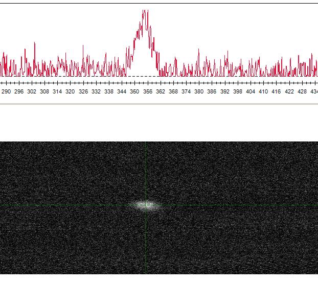


20 Particle Sensitivity (glass substrate) 90nm PSL 100nm PSL 20
21 Side Discrimination Glass Substrates Medium Scratch Defect on Side A Defect on Side B Signal (mv) Backside detection <0.2% Distance (um) The current head has less than 0.2% cross talk 21

22 Advanced Algorithm for Side Discrimination Most defects easily detected and side defined Scratch Shallow-Disk 5 Defect On Bottom Ghost Elimination 22
23 Summary Focus on optical testing Bit density vs. defect size Production concerns Optical testing pro and contra Detection requirements/challenges Throughput Xyratex sensor Concept Modularity Maps of main detector categories Contributors Andrei Brunfeld Bryan Clark Gregory Toker Morey Roscrow Peter Goglia Entire Titan project team 23
EUV Substrate and Blank Inspection
 EUV Substrate and Blank Inspection SEMATECH EUV Workshop 10/11/99 Steve Biellak KLA-Tencor RAPID Division *This work is partially funded by NIST-ATP project 98-06, Project Manager Purabi Mazumdar 1 EUV
Perpendicular Media - Metrology and Inspection Challenges. Sri Venkataram KLA-Tencor Corporation Sept 19, 2007
 Perpendicular Media - Metrology and Inspection Challenges Sri Venkataram KLA-Tencor Corporation Sept 19, 2007 Agenda Perpendicular Media Adoption PMR Metrology & Inspection Implementation Solutions Review
Dark Field Technologies
 Dark Field Technologies High Speed Solid State Laser Inspection of Flexible Substrates AIMCAL Meeting 2012 Solid State Laser Reflection (SSLR) Technology for Clear and Reflective Webs Laser Scanners Pros
Bringing Answers to the Surface
 3D Bringing Answers to the Surface 1 Expanding the Boundaries of Laser Microscopy Measurements and images you can count on. Every time. LEXT OLS4100 Widely used in quality control, research, and development
HDD Technology Trends
 R e s e a r c h HDD Technology Trends Dr. Richard New Director of Research Hitachi Global Storage Technologies HDD Technology Challenges Storage Technology Capabilities Storage Usage Requirements Storage
attocfm I for Surface Quality Inspection NANOSCOPY APPLICATION NOTE M01 RELATED PRODUCTS G
 APPLICATION NOTE M01 attocfm I for Surface Quality Inspection Confocal microscopes work by scanning a tiny light spot on a sample and by measuring the scattered light in the illuminated volume. First,
Point Autofocus Probe Surface Texture Measuring Instrument. PF-60 technical report
 Point Autofocus Probe Surface Texture Measuring Instrument PF-60 technical report ISO approved Mitaka measuring method for areal surface texture (ISO 25178-605) Document No, Title Published ISO 25178-6
Titelfoto. Advanced Laser Beam Shaping - for Optimized Process Results and Quality Inspection in the PV Production - Maja Thies.
 2010 LIMO Lissotschenko Mikrooptik GmbH www.limo.de Titelfoto Advanced Laser Beam Shaping - for Optimized Process Results and Quality Inspection in the PV Production - Maja Thies Photonics Key Technology
Resolution. Diffraction from apertures limits resolution. Rayleigh criterion θ Rayleigh = 1.22 λ/d 1 peak at 2 nd minimum. θ f D
 Microscopy Outline 1. Resolution and Simple Optical Microscope 2. Contrast enhancement: Dark field, Fluorescence (Chelsea & Peter), Phase Contrast, DIC 3. Newer Methods: Scanning Tunneling microscopy (STM),
Large Field of View, High Spatial Resolution, Surface Measurements
 Large Field of View, High Spatial Resolution, Surface Measurements James C. Wyant and Joanna Schmit WYKO Corporation, 2650 E. Elvira Road Tucson, Arizona 85706, USA jcwyant@wyko.com and jschmit@wyko.com
PhE102-VASE. PHE102 Variable Angle Spectroscopic Ellipsometer. Angstrom Advanced Inc. Angstrom Advanced. Angstrom Advanced
 Angstrom Advanced PhE102-VASE PHE102 Variable Angle Spectroscopic Ellipsometer Angstrom Advanced Instruments for Thin Film and Semiconductor Applications sales@angstromadvanced.com www.angstromadvanced.com
Sintec Optronics Technology Pte Ltd 10 Bukit Batok Crescent #07-02 The Spire Singapore Tel: Fax:
 Sintec Optronics Technology Pte Ltd 10 Bukit Batok Crescent #07-02 The Spire Singapore 658079 Tel: +65 63167112 Fax: +65 63167113 High-power Nd:YAG Self-floating Laser Cutting Head We supply the laser
Dr. Ralf Freiberger. TEMA GmbH / Mühlbauer Group
 Welcome to ADF&PCD Paris 2018 Inline Final Inspection of Aerosol Cans Dr. Ralf Freiberger TEMA GmbH / Mühlbauer Group Overview 1. Purpose 2. State of the Art: Integration in Line 3. New: Inspection at
450mm and Moore s Law Advanced Packaging Challenges and the Impact of 3D
 450mm and Moore s Law Advanced Packaging Challenges and the Impact of 3D Doug Anberg VP, Technical Marketing Ultratech SOKUDO Lithography Breakfast Forum July 10, 2013 Agenda Next Generation Technology
Lithography. Taking Sides to Optimize Wafer Surface Uniformity. Backside Inspection Applications In Lithography
 Lithography D E F E C T I N S P E C T I O N Taking Sides to Optimize Wafer Surface Uniformity Backside Inspection Applications In Lithography Kay Lederer, Matthias Scholze, Ulrich Strohbach, Infineon Technologies
The End of Thresholds: Subwavelength Optical Linewidth Measurement Using the Flux-Area Technique
 The End of Thresholds: Subwavelength Optical Linewidth Measurement Using the Flux-Area Technique Peter Fiekowsky Automated Visual Inspection, Los Altos, California ABSTRACT The patented Flux-Area technique
Sensor Fusion Enables Comprehensive Analysis of Laser Processing in Additive Manufacturing
 MKS Instruments 1 of 6 Sensor Fusion Enables Comprehensive Analysis of Laser Processing in Additive Manufacturing By Kevin Kirkham, Senior Manager, Product Development, Ophir Sensor: "A device that detects
GRADE A ENGRAVING. Application-focused DPSS laser outshines industry favorite fiber laser counterpart when marking components
 GRADE A ENGRAVING by Marin Iliev, R&D manager, RMI Laser Application-focused DPSS laser outshines industry favorite fiber laser counterpart when marking components No doubt fiber lasers are the most common
Enabling Areal Density Growth
 Shrinking the Magnetic Spacing for Advanced PMR Heads Diskcon Asia 2007 Enabling Areal Density Growth Shrinking the magnetic spacing remains one of the biggest levers for areal density growth! Areal Density
BEAM HALO OBSERVATION BY CORONAGRAPH
 BEAM HALO OBSERVATION BY CORONAGRAPH T. Mitsuhashi, KEK, TSUKUBA, Japan Abstract We have developed a coronagraph for the observation of the beam halo surrounding a beam. An opaque disk is set in the beam
LASER. Analog Laser Displacement Transducer. LAS Series. Key-Features:
 LASER Analog Laser Displacement Transducer LAS Series Key-Features: Content: Measurement Principle & Installation...2 Overview of the Series...3 Technical Data.4 Technical Drawing...7 Linearity & Resolution...8
Lecture 20: Optical Tools for MEMS Imaging
 MECH 466 Microelectromechanical Systems University of Victoria Dept. of Mechanical Engineering Lecture 20: Optical Tools for MEMS Imaging 1 Overview Optical Microscopes Video Microscopes Scanning Electron
Inspection. Wafer Inspection Technology Challenges for ULSI Manufacturing Part II F E A T U R E S
 Inspection F E A T U R E S Wafer Inspection Technology Challenges for ULSI Manufacturing Part II by Stan Stokowski, Ph.D., Chief Scientist; Mehdi Vaez-Irvani, Ph.D., Principal Research Scientist Continued
ASM Webinar Digital Microscopy for Materials Science
 Digital Microscopy Defined The term Digital Microscopy applies to any optical platform that integrates a digital camera and software to acquire images; macroscopes, stereomicroscopes, compound microscopes
High-Resolution Bubble Printing of Quantum Dots
 SUPPORTING INFORMATION High-Resolution Bubble Printing of Quantum Dots Bharath Bangalore Rajeeva 1, Linhan Lin 1, Evan P. Perillo 2, Xiaolei Peng 1, William W. Yu 3, Andrew K. Dunn 2, Yuebing Zheng 1,*
Nanonics Systems are the Only SPMs that Allow for On-line Integration with Standard MicroRaman Geometries
 Nanonics Systems are the Only SPMs that Allow for On-line Integration with Standard MicroRaman Geometries 2002 Photonics Circle of Excellence Award PLC Ltd, England, a premier provider of Raman microspectral
Coherent Laser Measurement and Control Beam Diagnostics
 Coherent Laser Measurement and Control M 2 Propagation Analyzer Measurement and display of CW laser divergence, M 2 (or k) and astigmatism sizes 0.2 mm to 25 mm Wavelengths from 220 nm to 15 µm Determination
Optical Components for Laser Applications. Günter Toesko - Laserseminar BLZ im Dezember
 Günter Toesko - Laserseminar BLZ im Dezember 2009 1 Aberrations An optical aberration is a distortion in the image formed by an optical system compared to the original. It can arise for a number of reasons
LED Displacement Sensor
 LED Displacement Sensor Low-cost LED Displacement Sensor Offers 10-micron Resolution of 25 mm (0.98 in) with measurement range of ±4 mm (0.16 in). Easy-to-use, built-in amplifier. Fast 5-millisecond response.
NON-AMPLIFIED HIGH SPEED PHOTODETECTOR USER S GUIDE
 NON-AMPLIFIED HIGH SPEED PHOTODETECTOR USER S GUIDE Thank you for purchasing your Non-amplified High Speed Photodetector. This user s guide will help answer any questions you may have regarding the safe
Rear Side Processing of Soda-Lime Glass Using DPSS Nanosecond Laser
 Lasers in Manufacturing Conference 215 Rear Side Processing of Soda-Lime Glass Using DPSS Nanosecond Laser Juozas Dudutis*, Paulius Gečys, Gediminas Račiukaitis Center for Physical Sciences and Technology,
State of the art EUV mask blank inspection with a Lasertec M7360 at the SEMATECH MBDC
 State of the art EUV mask blank inspection with a Lasertec M7360 at the SEMATECH MBDC Patrick Kearney a, Won-Il Cho a, Chan-Uk Jeon a, Eric Gullikson b, Anwei Jia c, Tomoya Tamura c, Atsushi Tajima c,
Fundamental Characterizations of Diamond Disc, Pad, and Retaining Ring Wear in Chemical Mechanical Planarization Processes
 Fundamental Characterizations of Diamond Disc, Pad, and Retaining Ring Wear in Chemical Mechanical Planarization Processes Yun Zhuang 1,2, Len Borucki 1, Ara Philipossian 1,2 1. Araca, Inc., Tucson, Arizona
Standard Operating Procedure of Atomic Force Microscope (Anasys afm+)
") Standard Operating Procedure of Atomic Force Microscope (Anasys afm+) The Anasys Instruments afm+ system incorporates an Atomic Force Microscope which can scan the sample in the contact mode and generate
Standard Operating Procedure of Atomic Force Microscope (Anasys afm+) The Anasys Instruments afm+ system incorporates an Atomic Force Microscope which can scan the sample in the contact mode and generate
attosnom I: Topography and Force Images NANOSCOPY APPLICATION NOTE M06 RELATED PRODUCTS G
 APPLICATION NOTE M06 attosnom I: Topography and Force Images Scanning near-field optical microscopy is the outstanding technique to simultaneously measure the topography and the optical contrast of a sample.
Experimental study of slider dynamics induced by contacts with disk asperities
 Microsyst Technol (2013) 19:1369 1375 DOI 10.1007/s00542-013-1822-z TECHNICAL PAPER Experimental study of slider dynamics induced by contacts with disk asperities Wenping Song Liane Matthes Andrey Ovcharenko
NON-AMPLIFIED PHOTODETECTOR USER S GUIDE
 NON-AMPLIFIED PHOTODETECTOR USER S GUIDE Thank you for purchasing your Non-amplified Photodetector. This user s guide will help answer any questions you may have regarding the safe use and optimal operation
SMART LASER SENSORS SIMPLIFY TIRE AND RUBBER INSPECTION
 PRESENTED AT ITEC 2004 SMART LASER SENSORS SIMPLIFY TIRE AND RUBBER INSPECTION Dr. Walt Pastorius LMI Technologies 2835 Kew Dr. Windsor, ON N8T 3B7 Tel (519) 945 6373 x 110 Cell (519) 981 0238 Fax (519)
White Paper CoverTest Compensation and Protection Layer Application System for Stamper and Disc
 White Paper CoverTest Compensation and Protection Layer Application System for Stamper and Disc Table of Contents 01. CoverTest in brief... 2 02. Overview... 3 03. CoverTest foil... 7 a. CoverTest design...
Fiber Optic Communications Communication Systems
 INTRODUCTION TO FIBER-OPTIC COMMUNICATIONS A fiber-optic system is similar to the copper wire system in many respects. The difference is that fiber-optics use light pulses to transmit information down
Deep- Space Optical Communication Link Requirements
 Deep- Space Optical Communication Link Requirements Professor Chester S. Gardner Department of Electrical and Computer Engineering University of Illinois cgardner@illinois.edu Link Equation: For a free-
Introduction Visible light is an electromagnetic wave, characterized by a wavelength, an amplitude
 Thin Film Interferences of SiO2 and TiO2 : Thickness and Iridescence Eman Mousa Alhajji North Carolina State University Department of Materials Science and Engineering MSE 355 Lab Report 201 A Matthew
LASER. Analog Laser Displacement Transducer. LAS Series. Key-Features:
 LASER Analog Laser Displacement Transducer LAS Series KeyFeatures: Content: Measurement Principle & Installation Overview of the Series Technical Data Technical Drawing Linearity & Resolution Order Code
Precision Cold Ablation Material Processing using High-Power Picosecond Lasers
 Annual meeting Burgdorf Precision Cold Ablation Material Processing using High-Power Picosecond Lasers Dr. Kurt Weingarten kw@time-bandwidth.com 26 November 2009 Background of Time-Bandwidth Products First
Dark Field Technologies In-Situ Defect Detection Practical Considerations and Results
 Dark Field Technologies In-Situ Defect Detection Practical Considerations and Results June 21, 2017 In-Situ Defect Detection The need for In-Situ Defect Detection Solid State Laser Reflection Practical
SUPRA Optix 3D Optical Profiler
 SUPRA Optix 3D Optical Profiler Scanning White-light Interferometric Microscope SWIM Series Applications The SUPRA Optix is the latest development in the field of Scanning White-light Interferometry. With
FUTURE PROSPECTS FOR CMOS ACTIVE PIXEL SENSORS
 FUTURE PROSPECTS FOR CMOS ACTIVE PIXEL SENSORS Dr. Eric R. Fossum Jet Propulsion Laboratory Dr. Philip H-S. Wong IBM Research 1995 IEEE Workshop on CCDs and Advanced Image Sensors April 21, 1995 CMOS APS
Review of Solidstate Photomultiplier. Developments by CPTA & Photonique SA
 Review of Solidstate Photomultiplier Developments by CPTA & Photonique SA Victor Golovin Center for Prospective Technologies & Apparatus (CPTA) & David McNally - Photonique SA 1 Overview CPTA & Photonique
CHAPTER 6 CARBON NANOTUBE AND ITS RF APPLICATION
 CHAPTER 6 CARBON NANOTUBE AND ITS RF APPLICATION 6.1 Introduction In this chapter we have made a theoretical study about carbon nanotubes electrical properties and their utility in antenna applications.
Säntis 300 Full wafer cathodoluminescence control up to 300 mm diameter
 Säntis 300 Full wafer cathodoluminescence control up to 300 mm diameter Overview The Säntis 300 system has been designed for fully automated control of 150, 200 and 300 mm wafers. Attolight s Quantitative
Hamidreza Karbasi, P. Eng., PhD Conestoga College ITAL Oct. 7, 2010
 Presented at the COMSOL Conference 2010 Boston Presented by: Hamidreza Karbasi, P. Eng., PhD Conestoga College ITAL Oct. 7, 2010 Creating and Building Sustainable Environments Outline Background Objectives
Examination Optoelectronic Communication Technology. April 11, Name: Student ID number: OCT1 1: OCT 2: OCT 3: OCT 4: Total: Grade:
 Examination Optoelectronic Communication Technology April, 26 Name: Student ID number: OCT : OCT 2: OCT 3: OCT 4: Total: Grade: Declaration of Consent I hereby agree to have my exam results published on
Exercise 8: Interference and diffraction
 Physics 223 Name: Exercise 8: Interference and diffraction 1. In a two-slit Young s interference experiment, the aperture (the mask with the two slits) to screen distance is 2.0 m, and a red light of wavelength
plasmonic nanoblock pair
 Nanostructured potential of optical trapping using a plasmonic nanoblock pair Yoshito Tanaka, Shogo Kaneda and Keiji Sasaki* Research Institute for Electronic Science, Hokkaido University, Sapporo 1-2,
All-Glass Gray Scale PhotoMasks Enable New Technologies. Che-Kuang (Chuck) Wu Canyon Materials, Inc.
 Wu Canyon Materials, Inc.") All-Glass Gray Scale PhotoMasks Enable New Technologies Che-Kuang (Chuck) Wu Canyon Materials, Inc. 1 Overview All-Glass Gray Scale Photomask technologies include: HEBS-glasses and LDW-glasses HEBS-glass
All-Glass Gray Scale PhotoMasks Enable New Technologies Che-Kuang (Chuck) Wu Canyon Materials, Inc. 1 Overview All-Glass Gray Scale Photomask technologies include: HEBS-glasses and LDW-glasses HEBS-glass
Optical Microscopy and Imaging ( Part 2 )
") 1 Optical Microscopy and Imaging ( Part 2 ) Chapter 7.1 : Semiconductor Science by Tudor E. Jenkins Saroj Kumar Patra, Department of Electronics and Telecommunication, Norwegian University of Science and
1 Optical Microscopy and Imaging ( Part 2 ) Chapter 7.1 : Semiconductor Science by Tudor E. Jenkins Saroj Kumar Patra, Department of Electronics and Telecommunication, Norwegian University of Science and
Non-amplified Photodetectors
 Non-amplified Photodetectors User Guide (800)697-6782 sales@eotech.com www.eotech.com Page 1 of 9 EOT NON-AMPLIFIED PHOTODETECTOR USER S GUIDE Thank you for purchasing your Non-amplified Photodetector
PHY 431 Homework Set #5 Due Nov. 20 at the start of class
 PHY 431 Homework Set #5 Due Nov. 0 at the start of class 1) Newton s rings (10%) The radius of curvature of the convex surface of a plano-convex lens is 30 cm. The lens is placed with its convex side down
Chapter 4: Fourier Optics
 Chapter 4: Fourier Optics P4-1. Calculate the Fourier transform of the function rect(2x)rect(/3) The rectangular function rect(x) is given b 1 x 1/2 rect( x) when 0 x 1/2 P4-2. Assume that ( gx (, )) G
Correlation of Wafer Backside Defects to Photolithography Hot Spots Using Advanced Macro Inspection
 Correlation of Wafer Defects to Photolithography Hot Spots Using Advanced Macro Inspection Alan Carlson* a, Tuan Le* a a Rudolph Technologies, 4900 West 78th Street, Bloomington, MN, USA 55435; Presented
Diffraction Single-slit Double-slit Diffraction grating Limit on resolution X-ray diffraction. Phys 2435: Chap. 36, Pg 1
 Diffraction Single-slit Double-slit Diffraction grating Limit on resolution X-ray diffraction Phys 2435: Chap. 36, Pg 1 Single Slit New Topic Phys 2435: Chap. 36, Pg 2 Diffraction: bending of light around
Measurement of Surface Profile and Layer Cross-section with Wide Field of View and High Precision
 Hitachi Review Vol. 65 (2016), No. 7 243 Featured Articles Measurement of Surface Profile and Layer Cross-section with Wide Field of View and High Precision VS1000 Series Coherence Scanning Interferometer
Copyright 2000 Society of Photo Instrumentation Engineers.
 Copyright 2000 Society of Photo Instrumentation Engineers. This paper was published in SPIE Proceedings, Volume 4043 and is made available as an electronic reprint with permission of SPIE. One print or
Comparison of actinic and non-actinic inspection of programmed defect masks
 Comparison of actinic and non-actinic inspection of programmed defect masks Funded by Kenneth Goldberg, Anton Barty Hakseung Han*, Stefan Wurm*, Patrick Kearney, Phil Seidel Obert Wood*, Bruno LaFontaine
SUPPLEMENTARY INFORMATION
 SUPPLEMENTARY INFORMATION doi:0.038/nature727 Table of Contents S. Power and Phase Management in the Nanophotonic Phased Array 3 S.2 Nanoantenna Design 6 S.3 Synthesis of Large-Scale Nanophotonic Phased
A tracking detector to study O(1 GeV) ν μ CC interactions
 ν μ CC interactions") A tracking detector to study O(1 GeV) ν μ CC interactions Laura Pasqualini on behalf of the mm-tracker Collaboration IPRD16, 3-6 October 2016, Siena Motivations ν/μ Tracking system for a light magnetic
A tracking detector to study O(1 GeV) ν μ CC interactions Laura Pasqualini on behalf of the mm-tracker Collaboration IPRD16, 3-6 October 2016, Siena Motivations ν/μ Tracking system for a light magnetic
New Lasers Improve Glass Cutting Methods
 New Lasers Improve Glass Cutting Methods Over the past decade, glass has become an increasingly sophisticated structural and functional component in uses as varied as flat panel displays (FPDs), automobiles
Non-amplified High Speed Photodetectors
 Non-amplified High Speed Photodetectors User Guide (800)697-6782 sales@eotech.com www.eotech.com Page 1 of 6 EOT NON-AMPLIFIED HIGH SPEED PHOTODETECTOR USER S GUIDE Thank you for purchasing your Non-amplified
arxiv:hep-ex/ v1 19 Apr 2002
 STUDY OF THE AVALANCHE TO STREAMER TRANSITION IN GLASS RPC EXCITED BY UV LIGHT. arxiv:hep-ex/0204026v1 19 Apr 2002 Ammosov V., Gapienko V.,Kulemzin A., Semak A.,Sviridov Yu.,Zaets V. Institute for High
Diffuser / Homogenizer - diffractive optics
 Diffuser / Homogenizer - diffractive optics Introduction Homogenizer (HM) product line can be useful in many applications requiring a well-defined beam shape with a randomly-diffused intensity profile.
Fiber Optic Communications
 Fiber Optic Communications ( Chapter 2: Optics Review ) presented by Prof. Kwang-Chun Ho 1 Section 2.4: Numerical Aperture Consider an optical receiver: where the diameter of photodetector surface area
Ti/Au TESs as photon number resolving detectors
 Ti/Au TESs as photon number resolving detectors LAPO LOLLI, E. MONTICONE, C. PORTESI, M. RAJTERI, E. TARALLI SIF XCVI National Congress, Bologna 20 24 September 2010 1 Introduction: What are TES? TESs
2. Pulsed Acoustic Microscopy and Picosecond Ultrasonics
 1st International Symposium on Laser Ultrasonics: Science, Technology and Applications July 16-18 2008, Montreal, Canada Picosecond Ultrasonic Microscopy of Semiconductor Nanostructures Thomas J GRIMSLEY
Measurement of Microscopic Three-dimensional Profiles with High Accuracy and Simple Operation
 238 Hitachi Review Vol. 65 (2016), No. 7 Featured Articles Measurement of Microscopic Three-dimensional Profiles with High Accuracy and Simple Operation AFM5500M Scanning Probe Microscope Satoshi Hasumura
KNIFE-EDGE RIGHT-ANGLE PRISM MIRRORS
 KNIFE-EDGE RIGHT-ANGLE PRISM MIRRORS Precision Cut Prisms Feature Bevel-Free 90 Angle Dielectric, Silver, Gold, and Aluminum Coatings Available 25 mm x 25 mm Faces Application Idea MRAK25-M01 Mounted on
EE119 Introduction to Optical Engineering Spring 2003 Final Exam. Name:
 EE119 Introduction to Optical Engineering Spring 2003 Final Exam Name: SID: CLOSED BOOK. THREE 8 1/2 X 11 SHEETS OF NOTES, AND SCIENTIFIC POCKET CALCULATOR PERMITTED. TIME ALLOTTED: 180 MINUTES Fundamental
PHYS 241 FINAL EXAM December 11, 2006
 1. (5 points) Light of wavelength λ is normally incident on a diffraction grating, G. On the screen S, the central line is at P and the first order line is at Q, as shown. The distance between adjacent
Design and Performance of a Pinned Photodiode CMOS Image Sensor Using Reverse Substrate Bias
 Design and Performance of a Pinned Photodiode CMOS Image Sensor Using Reverse Substrate Bias 13 September 2017 Konstantin Stefanov Contents Background Goals and objectives Overview of the work carried
2009 International Workshop on EUV Lithography
 Contents Introduction Absorber Stack Optimization Non-flatness Correction Blank Defect and Its Mitigation Wafer Printing Inspection Actinic Metrology Cleaning and Repair Status Remaining Issues in EUV
E-Beam Hard Disk Drive Using Gated Carbon Nano Tube Source and Phase Change Media
 E-Beam Hard Disk Drive Using Gated Carbon Nano Tube Source and Phase Change Media William S. Oakley NanoScale Storage Systems, Inc willoakley1@earthlink.net Abstract A novel high speed, high capacity electron-beam
Photoacoustic Imaging of Blood Vessels in Tissue
 of Blood Vessels in Tissue F.F.M. de Mul (University of Twente, Enschede, the Netherlands) FdM [µm] Imaging methods for hidden structures in turbid media (tissue) OCT/ OPS (C)M TOF / FM NIR green C(M)
Surface Finish Measurement Methods and Instrumentation
 125 years of innovation Surface Finish Measurement Methods and Instrumentation Contents Visual Inspection Surface Finish Comparison Plates Contact Gauges Inductive / Variable Reluctance (INTRA) Piezo Electric
Computer Generated Holograms for Optical Testing
 Computer Generated Holograms for Optical Testing Dr. Jim Burge Associate Professor Optical Sciences and Astronomy University of Arizona jburge@optics.arizona.edu 520-621-8182 Computer Generated Holograms
Sensitive measurement of partial coherence using a pinhole array
 1.3 Sensitive measurement of partial coherence using a pinhole array Paul Petruck 1, Rainer Riesenberg 1, Richard Kowarschik 2 1 Institute of Photonic Technology, Albert-Einstein-Strasse 9, 07747 Jena,
Mask Technology Development in Extreme-Ultraviolet Lithography
 Mask Technology Development in Extreme-Ultraviolet Lithography Anthony Yen September 6, 2013 Projected End of Optical Lithography 2013 TSMC, Ltd 1976 1979 1982 1985 1988 1991 1994 1997 2000 2003 2007 2012
1 Propagating Light. Reflection and Refraction
 PRACTICE FINAL 1 1) An ac source of period T and maximum voltage V is connected to a single unknown ideal element that is either a resistor, and inductor, or a capacitor. At time t = 0 the voltage is zero.
The Wave Nature of Light
 The Wave Nature of Light Physics 102 Lecture 7 4 April 2002 Pick up Grating & Foil & Pin 4 Apr 2002 Physics 102 Lecture 7 1 Light acts like a wave! Last week we saw that light travels from place to place
The below identified patent application is available for licensing. Requests for information should be addressed to:
 DEPARTMENT OF THE NAVY OFFICE OF COUNSEL NAVAL UNDERSEA WARFARE CENTER DIVISION 1176 HOWELL STREET NEWPORT Rl 0841-1708 IN REPLY REFER TO Attorney Docket No. 300048 7 February 017 The below identified
GenePix Application Note
 GenePix Application Note Biological Relevance of GenePix Results Shawn Handran, Ph.D. and Jack Y. Zhai, Ph.D. Axon Instruments, Inc. 3280 Whipple Road, Union City, CA 94587 Last Updated: Aug 22, 2003.
3D Optical Motion Analysis of Micro Systems. Heinrich Steger, Polytec GmbH, Waldbronn
 3D Optical Motion Analysis of Micro Systems Heinrich Steger, Polytec GmbH, Waldbronn SEMICON Europe 2012 Outline Needs and Challenges of measuring Micro Structure and MEMS Tools and Applications for optical
INTRODUCTION 提夫自控技术 ( 上海 ) 有限公司 LAS laser sensors cover measurement ranges from 1 to mm. The integrated micro-controller delivers an accur
 有限公司 LAS laser sensors cover measurement ranges from 1 to mm. The integrated micro-controller delivers an accur") LASER Analog Laser Displacement Transducer LAS Series Key-Features: Content: Measurement Principle & Installation...2 Overview of the Series...3 Technical Data.4 Technical Drawings...9 Diagrams...10 Order
LASER Analog Laser Displacement Transducer LAS Series Key-Features: Content: Measurement Principle & Installation...2 Overview of the Series...3 Technical Data.4 Technical Drawings...9 Diagrams...10 Order
Manufacturing Metrology Team
 The Team has a range of state-of-the-art equipment for the measurement of surface texture and form. We are happy to discuss potential measurement issues and collaborative research Manufacturing Metrology
HIGH SPEED FIBER PHOTODETECTOR USER S GUIDE
 HIGH SPEED FIBER PHOTODETECTOR USER S GUIDE Thank you for purchasing your High Speed Fiber Photodetector. This user s guide will help answer any questions you may have regarding the safe use and optimal
Microphotonics Readiness for Commercial CMOS Manufacturing. Marco Romagnoli
 Microphotonics Readiness for Commercial CMOS Manufacturing Marco Romagnoli MicroPhotonics Consortium meeting MIT, Cambridge October 15 th, 2012 Passive optical structures based on SOI technology Building
Radial Polarization Converter With LC Driver USER MANUAL
 ARCoptix Radial Polarization Converter With LC Driver USER MANUAL Arcoptix S.A Ch. Trois-portes 18 2000 Neuchâtel Switzerland Mail: info@arcoptix.com Tel: ++41 32 731 04 66 Principle of the radial polarization
DATA SHEET. OD Precision. Displacement sensors for precise and comprehensive measurement tasks
 DATA SHEET OD Precision Displacement sensors for precise and comprehensive measurement tasks OD Precision Displacement sensors for precise and comprehensive measurement tasks Displacement sensors from
Capabilities of Flip Chip Defects Inspection Method by Using Laser Techniques
 Capabilities of Flip Chip Defects Inspection Method by Using Laser Techniques Sheng Liu and I. Charles Ume* School of Mechanical Engineering Georgia Institute of Technology Atlanta, Georgia 3332 (44) 894-7411(P)
VISUAL PHYSICS ONLINE DEPTH STUDY: ELECTRON MICROSCOPES
 VISUAL PHYSICS ONLINE DEPTH STUDY: ELECTRON MICROSCOPES Shortly after the experimental confirmation of the wave properties of the electron, it was suggested that the electron could be used to examine objects
Advanced 3D Optical Profiler using Grasshopper3 USB3 Vision camera
 Advanced 3D Optical Profiler using Grasshopper3 USB3 Vision camera Figure 1. The Zeta-20 uses the Grasshopper3 and produces true color 3D optical images with multi mode optics technology 3D optical profiling
APPLICATION NOTE. Understanding the PV Specification. Introduction. Problems with PV
 APPLICATION NOTE Understanding the PV Specification Introduction An array of non-standard, arbitrary practices are frequently used in the optics industry to demonstrate conformance of a part to the traditional