DDR Verification Approaches. designinsight seminar
|
|
|
- Alberta Wade
- 6 years ago
- Views:
Transcription


1 DDR Verification Approaches designinsight seminar

 Complexity of JEDEC Conformance Tests Vref / Vih / Vil")

2 DDR Test Challenges Signal Access & Probing Easy-to-use / reliable connections Bandwidth & Signal Integrity Affordable Isolation of Read/Write bursts Triggering or Post-Processing (ASM) Complexity of JEDEC Conformance Tests Vref / Vih / Vil Derating Results Validity / Statistics Effective Reporting / Archiving Advanced Analysis Characterization Debug 2 designinsight seminar


3 Challenge 1: Probing DDR Memory Computer Systems use standardized DIMM s for which several probing solutions are available Memory in Embedded Designs is usually directly mounted on the PCB All DDR2 & DDR3 Components use BGA Packages Probing a BGA package is Difficult Unable to probe at the Balls of the Device Signal Access Solutions Component Interposers Direct Probing Analog Probing DQ, DQS, Clock Digital Probing Address Command Power, Reset, and Reference Component Interposer Analog and Digital Probing 3 designinsight seminar *Courtesy Micron Technologies Direct Probing


4 Analog Solder-In Probing Solutions for DDR P7500 Series Tri-Mode Probes Socket Cable xx TriMode Micro-Coax Tip 4GHz P75TRLST Solder Tip up to 20GHz 4 designinsight seminar


5 Nexus DDR3 BGA Chip Interposers For Oscilloscopes Retention Socket BGA Chip Interposer 5 designinsight seminar
 6 designinsight")
6 BGA Chip Access For DDR2, DDR3 Unique, reusable socket design allows for multiple chip exchanges Able to use both analog and digital probes Nexus DDR Interposers sold by Tektronix DDR2 and DDR3 versions X4/x8, x16 pins Socket and solder models (See MSR for details) 6 designinsight seminar

7 BGA Chip Interposer Signal Fidelity Filters are available to de-embed analog effects Library of filters is provided with the interposer Filters were developed based on the actual S-parameters of the interposer + probe tip Available for DPO/DSA/MSO70000 and DPO7000 scopes Eye - unfiltered Eye with filter 7 designinsight seminar
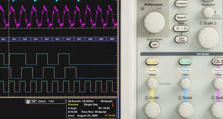
 Locate the precise edges of each burst")
 DDR3 Read Burst DDR3 Write Burst 8")
8 Challenge 2: Burst Identification Locate the right kind of bursts (read vs write) Locate the precise edges of each burst Refine burst identity based on other criteria (rank, secondary bus state, etc) DDR3 Read Burst DDR3 Write Burst 8 designinsight seminar
 9 designinsight")
9 HW Triggering on DDR Reads / Writes Window Trigger - useful for real-time DDR read /write isolation DQS goes high for writes, low for reads (DDR3) 9 designinsight seminar
10 Advanced Search & Mark (ASM) and Long Records Easily identify & measure all Read / Write bursts in the acquisition Based on the Advanced Search & Mark feature Scroll through marked reads / writes across the entire waveform record 10 designinsight seminar

11 Burst Identification on an MSO Using bus state, specific transactions can be isolated For example, locate only Reads from a specific memory rank Advanced Search & Mark is used for fine burst positioning 11 designinsight seminar


12 Challenge 3: Measurement Setup JEDEC Standards specify measurements & methods 12 designinsight seminar

13 Ease of Use - DDRA Wizard Step #1 Select DDR Generation Select DDR Rate Step #2 13 designinsight seminar Choose measurements (Read / Write / CLK / Addr & Command)
14 Comprehensive Measurement Support Option DDRA supports a broad range of JEDEC-specified measurements for DDR, DDR2, DDR3, LP-DDR Example measurements list for DDR2 : tipw tis (base) tck(avg) tds - diff (base) tih (base) tck(abs) tds - SE (base) tis - DERATED tch(avg) tds -diff - DERATED tih - DERATED tch(abs) tds -SE - DERATED Vid - diff (AC) tcl(avg) tdh - diff (base) Vix (AC) - DQS tcl(abs) tdh - SE (base) Vix (AC) - CLK thp tdh -diff - DERATED Vox (AC) - DQS tjit(duty) tdh -SE - DERATED Vox (AC) - CLK tjit(per) tdipw Input Slew-Rise (DQS), tjit(cc) tac - diff terr(02) tdqsck -diff Input Slew-Fall (DQS), terr(03) tdqsck - SE Input Slew-Rise (CLK), terr(04) tdqsq - diff Input Slew-Fall (CLK), terr(05) tdqsq - SE AC - Overshoot Amplitude - diff terr( 6-10 per) tqh AC -Undershoot Amplitude - diff terr(11-50 per) tdqss AC - Overshoot Amplitude - SE tdqsh tdss AC - Undershoot Amplitude - SE tdsh Data Eye Width 14 designinsight seminar
15 Measurement De-rating JEDEC stipulates de-rating of DDR2 and DDR3 pass / fail limits for Setup & Hold measurements based on signal slew rate* Option DDRA automatically calculates slew rates and applies the appropriate de-rating values to the measurement limits. tds - diff (base) tds -diff - DERATED tds - SE (base) tds -SE - DERATED tdh - diff (base) tdh -diff - DERATED tdh - SE (base) tdh -SE - DERATED tis (base) tis - DERATED tih (base) tih - DERATED 15 designinsight seminar * JESD79-2E, JESD79-3C specifications

16 Challenge 4: Results and Statistical Validity To have confidence in your test results, you need 100 s, 1000 s or even more observations of each measurement As a practical matter, measurement throughput is essential 16 designinsight seminar

17 Challenge 5: Reporting and Archiving HTML Reports Source Waveforms 17 designinsight seminar

18 Challenge 6: Advanced Analysis and Debug DDRA has access to all plotting & debug tools in DPOJET 18 designinsight seminar

19 DDR Analog Validation & Debug Tektronix Solutions Signal Access - Probing P7500 TriMode Probing Single probe for diff, CM and single-ended measurements Up to 20 GHz bandwidth to the probe tip P6780 Logic Probe 16 channel Active Differential probe with 2.5 GHz bandwidth Socketed BGA interposers for multiple exchanges Signal Acquisition Automatically trigger and capture DDR signals Identify and trigger directly on DQ, DQS in real-time to isolate Reads/Writes Command Bus triggering with user-defined decode files Capture long time duration at high resolution Direct connection to DPOJET for signal analysis Time trend view for analysis of low frequency effects Signal Analysis DDRA Automated setup, read/write burst detection, JEDEC pass/fail meas. DPOJET The most powerful Jitter, Eye and Timing analysis tool Time, Amplitude, Histogram, measurements Advanced Jitter, Eye diagram measurements and Pass/Fail testing Many display and plotting options Report generator 19 designinsight seminar
20 Resources Tektronix Knowledge Center: DDR Application Note: 20 designinsight seminar
Jerry Chu 2010/08/23 Vincent Chang 2010/08/23
 Product Model Name: AD1U400A1G3 Product Specification: DDR-400(CL3) 184-Pin U-DIMM 1GB (128M x 64-bits) Issuing Date: 2010/08/23 Version: 0 Item: 1. General Description 2. Features 3. Pin Assignment 4.
Industrial DDR SO-DIMM Information. Features
 Industrial DDR3 1333 SODIMM Information Part Number Capacity Organization Rank Height DIMM type Note TS256MSK64V3NI 2GB 256Mx8 1 30.00mm SODIMM antisulfur Features 1. Operating Temperature : 40 C to +85
REV /2003 NANYA TECHNOLOGY CORP. NANYA TECHNOLOGY CORP. reserves the right to change Products and Specifications without notice.
 200pin Unbuffered DDR SO-DIMM Based on DDR333/266 16Mx16 SDRAM Features JEDEC Standard 200-Pin Small Outline Dual In-Line Memory Module (SO-DIMM) 32Mx64 Double Unbuffered DDR SO-DIMM based on 16Mx16 DDR
REV /2010 NANYA TECHNOLOGY CORP. NANYA TECHNOLOGY CORP. reserves the right to change Products and Specifications without notice.
 240pin Unbuffered DDR2 SDRAM MODULE Based on 128Mx8 DDR2 SDRAM G-die Features Performance: PC2-5300 PC2-6400 PC2-8500 Speed Sort -3C -AC -BD DIMM Latency * 5 5 6 f CK Clock Frequency 333 400 533 MHz t
Visual Triggering. Technical Brief
 Visual Triggering Technical Brief Capturing and finding the right characteristic of a complex signal can require hours of collecting and sorting through thousands of acquisitions for the event of interest.
512MB Unbuffered DDR2 SDRAM DIMM
 512MB Unbuffered DDR2 SDRAM DIMM (64M words 64 bits, 1 Rank) Specifications Density: 512MB Organization 64M words 64 bits, 1 rank Mounting 8 pieces of 512M bits DDR2 SDRAM sealed in FBGA Package: 240-pin
512Mb DDRII SDRAM Specification
 512Mb DDRII SDRAM Specification P3R12E30CBF Deutron Electronics Corp. Deutron Electronics Corp. V1.0 Specifications Features Density: 512M bits Organization 16M words 8 bits 4 banks (P3R12E30CBF) 8M words
A Time-Saving Method for Analyzing Signal Integrity in DDR Memory Buses
 A Time-Saving Method for Analyzing Signal Integrity in DDR Memory Buses Application Note 1591 This application note covers new tools and measurement techniques for characterizing and validating signal
Soldering a P7500 to a Nexus DDR Component Interposer
 Soldering a P7500 to a Nexus DDR Component Interposer Introduction This document shows an example of how to solder P7500 tips to the oscilloscope version of a Nexus DDR Component Interposer board. The
NT256D64S88AMGM is an unbuffered 200-Pin Double Data Rate (DDR) Synchronous DRAM Dual In-Line Memory Module (DIMM),
 Synchronous DRAM Dual In-Line Memory Module (DIMM),") 200pin One Bank Unbuffered DDR SO-DIMM Based on DDR266/200 32Mx8 SDRAM Features JEDEC Standard 200-Pin Small Outline Dual In-Line Memory Module (SO-DIMM) 32Mx64 Double Unbuffered DDR SO-DIMM based on 32Mx8
200pin One Bank Unbuffered DDR SO-DIMM Based on DDR266/200 32Mx8 SDRAM Features JEDEC Standard 200-Pin Small Outline Dual In-Line Memory Module (SO-DIMM) 32Mx64 Double Unbuffered DDR SO-DIMM based on 32Mx8
UFS v2.0 PHY and Protocol Testing for Compliance. Copyright 2013 Chris Loberg, Tektronix
 UFS v2.0 PHY and Protocol Testing for Compliance Copyright 2013 Chris Loberg, Tektronix Agenda Introduction to MIPI Architecture & Linkage to UFS Compliance Testing Ecosystem UFS Testing Challenges Preparing
Approval Sheet. Rev 1.0 DDR2 UDIMM. Customer M2UK-1GSF7C06-J. Product Number PC Module speed. 240 Pin. Pin. Operating Temp 0 C ~ 85 C
 Approval Sheet Customer Product Number Module speed Pin M2UK-1GSF7C06-J PC2-6400 240 Pin CL-tRCD-tRP 6-6-6 Operating Temp 0 C ~ 85 C Date 25 th Approval by Customer P/N: Signature: Date: Sales: Sr. Technical
icapture TM Analog MUX
 icapture TM Analog MUX WHITEPAPER Introduction icapture Analog MUX is a unique Tektronix innovation for viewing an electrical signal in digital and analog forms simultaneously using a single voltage probe.
D59C1512(404/804/164) ZT HIGH PERFORMANCE 512 Mbit DDR2 SDRAM 4 BANKS X 32Mbit X 4 (404) 4 BANKS X 16Mbit X 8 (804) 4 BANKS X 8Mbit X 16 (164)
 ZT HIGH PERFORMANCE 512 Mbit DDR2 SDRAM 4 BANKS X 32Mbit X 4 (404) 4 BANKS X 16Mbit X 8 (804) 4 BANKS X 8Mbit X 16 (164)") HIGH PERFORMANCE 512 Mbit DDR2 SDRAM 4 BANKS X 32Mbit X 4 (404) 4 BANKS X 16Mbit X 8 (804) 4 BANKS X 8Mbit X 16 (164) 37 3 25A 25 19A DDR2-533 DDR2-667 DDR2-800 DDR2-800 DDR2-1066 Clock Cycle Time (t CK3
HIGH PERFORMANCE 512 Mbit DDR2 SDRAM 4 BANKS X 32Mbit X 4 (404) 4 BANKS X 16Mbit X 8 (804) 4 BANKS X 8Mbit X 16 (164) 37 3 25A 25 19A DDR2-533 DDR2-667 DDR2-800 DDR2-800 DDR2-1066 Clock Cycle Time (t CK3
High Speed Digital Design & Verification Seminar. Measurement fundamentals
 High Speed Digital Design & Verification Seminar Measurement fundamentals Agenda Sources of Jitter, how to measure and why Importance of Noise Select the right probes! Capture the eye diagram Why measure
Digital and Mixed Signal Oscilloscopes MSO/DPO70000 Series Datasheet
 Digital and Mixed Signal Oscilloscopes MSO/DPO70000 Series Datasheet Four-channel Simultaneous Performance Up to 23 GHz Bandwidth Up to 50 GS/s Real-time Sample Rate Up to 500 Megasample Record Length
A3R12E30CBF A3R12E40CBF
 512Mb DDRII SDRAM Specification A3R12E30CBF Industrial Version Zentel Electronics Corp. I Revision 1.0 Specifications Features Density: 512M bits Organization 16M words 8 bits 4 banks (A3R12E30CBF) 8M
512Mb DDRII SDRAM Specification A3R12E30DBF A3R12E40DBF
 512Mb DDRII SDRAM Specification A3R12E30DBF Zentel Electronics Corp. Specifications Features Density: 512 bits Organization 16M words 8 bits 4 banks (A3R12E30DBF) 8M words 16 bits 4 banks () Package 60-ball
EtronTech EM6A M x 16 DDR Synchronous DRAM (SDRAM)
") EtronTech EM6A9160 8M x 16 DDR Synchronous DRAM (SDRAM) (Rev. 1.4 May/2006) Features Pin Assignment (Top View) Fast clock rate: 300/275/250/200MHz Differential Clock & / Bi-directional DQS DLL enable/disable
EtronTech EM6A9160 8M x 16 DDR Synchronous DRAM (SDRAM) (Rev. 1.4 May/2006) Features Pin Assignment (Top View) Fast clock rate: 300/275/250/200MHz Differential Clock & / Bi-directional DQS DLL enable/disable
Getting Started. MSO/DPO Series Oscilloscopes. Basic Concepts
 Getting Started MSO/DPO Series Oscilloscopes Basic Concepts 001-1523-00 Getting Started 1.1 Getting Started What is an oscilloscope? An oscilloscope is a device that draws a graph of an electrical signal.
Product Specifications
 Product Specificatio M383L2923E-CC L383L2923E-CC RE: General Information 1GB 128MX72 DDR SDRAM REGISTERED 18 PIN DIMM ECC Description: The M/L383L2923E is a 128M X 72 Double Data Rate SDRAM high deity
R&S RTO-K92 emmc Compliance Test Test Procedures
 R&S RTO-K92 emmc Compliance Test Test Procedures (=Q3Þ2) Test Procedures 1333.0380.02 03 This manual describes the emmc compliance test procedures with the following options: R&S RTO-K92 (1329.6958.02)/(1333.0444.02)
184PIN DDR333 Unbuffered DIMM 256MB With 32Mx8 CL2.5. Description. Placement. Features PCB : Transcend Information Inc. 1
 Description Placement The TS32MLD64V3F5 is a 32M x 64bits Double Data Rate high-density for 333. The TS32MLD64V3F5 consists of 8pcs CMOS 32Mx8 bits Double Data Rate s in 66 pin TSOP-II 400mil packages
HY5DU Banks x 8M x 8Bit Double Data Rate SDRAM
 4 Banks x 8M x 8Bit Double Data Rate SDRAM PRELIMINARY DESCRIPTION The Hyundai HY5DU56822 is a 268,435,456-bit CMOS Double Data Rate(DDR) Synchronous DRAM, ideally suited for the main memory applications
TriMode Probe Family. P7500 Series Datasheet. Features & Benefits. Applications
 TriMode Probe Family P7500 Series Datasheet P7516 with optional P75PDPM Features & Benefits TriMode Probe One Setup, Three Measurements without Adjusting Probe Tip Connections Differential Single Ended
A Solution of Test, Inspection and Evaluation for Blind Signal Waveform on a Board
 A Solution of Test, Inspection and Evaluation for Blind Signal Waveform on a Board Tatsumi Watabe, Makoto Kawamura, & Hiroyuki Yamakoshi S.E.R. Corporation Conference Ready mm/dd/2014 2016 BiTS Workshop
Digital Debug With Oscilloscopes Lab Experiment
 Digital Debug With Oscilloscopes A collection of lab exercises to introduce you to digital debugging techniques with a digital oscilloscope. Revision 1.0 Page 1 of 23 Revision 1.0 Page 2 of 23 Copyright
In this lecture, we will first examine practical digital signals. Then we will discuss the timing constraints in digital systems.
 1 In this lecture, we will first examine practical digital signals. Then we will discuss the timing constraints in digital systems. The important concepts are related to setup and hold times of registers
Keysight N6462A/N6462B DDR4 Compliance Test Application
 Keysight N6462A/N6462B DDR4 Compliance Test Application Methods of Implementation Notices Keysight Technologies 2014-2018 No part of this manual may be reproduced in any form or by any means (including
W9464G6KH 1M 4 BANKS 16 BITS DDR SDRAM. Table of Contents-
 1M 4 BANKS 16 BITS DDR SDRAM Table of Contents- 1. GENERAL DESCRIPTION... 4 2. FEATURES... 4 3. ORDER INFORMATION... 4 4. KEY PARAMETERS... 5 5. PIN CONFIGURATION... 6 6. PIN DESCRIPTION... 7 7. BLOCK
HY5DV Banks x 1M x 16Bit DOUBLE DATA RATE SDRAM
 4 Banks x M x 6Bit DOUBLE DATA RATE SDRAM PRELIMINARY DESCRIPTION The Hyundai is a 67,08,864-bit CMOS Double Data Rate(DDR) Synchronous DRAM, ideally suited for the point to point applications which require
W9412G2IB 1M 4 BANKS 32 BITS GDDR SDRAM. Table of Contents- Publication Release Date: Aug. 30, Revision A06
 1M 4 BANKS 32 BITS GDDR SDRAM Table of Contents- 1. GENERAL DESCRIPTION...4 2. FEATURES...4 3. KEY PARAMETERS...5 4. BALL CONFIGURATION...6 5. BALL DESCRIPTION...7 6. BLOCK DIAGRAM...9 7. FUNCTIONAL DESCRIPTION...10
W9425G6KH 4 M 4 BANKS 16 BITS DDR SDRAM. Table of Contents- Publication Release Date: Jul. 02, Revision: A01
 4 M 4 BANKS 16 BITS DDR SDRAM Table of Contents- 1. GENERAL DESCRIPTION... 4 2. FEATURES... 4 3. ORDER INFORMATION... 4 4. KEY PARAMETERS... 5 5. PIN CONFIGURATION... 6 6. PIN DESCRIPTION... 7 7. BLOCK
Revision History Revision 1.0 (July, 2003) - First release Revision 1.1 (August, 2003) - Finalized Revision 1.2 (March, 2004) - Corrected package dime
 - First release Revision 1.1 (August, 2003) - Finalized Revision 1.2 (March, 2004) - Corrected package dime") Unbuffered SODIMM (DDR400 Module) 200pin Unbuffered SODIMM based on 256Mb E-die 64/72-bit ECC/Non ECC Revision 1.2 March. 2004 Revision History Revision 1.0 (July, 2003) - First release Revision 1.1 (August,
Unbuffered SODIMM (DDR400 Module) 200pin Unbuffered SODIMM based on 256Mb E-die 64/72-bit ECC/Non ECC Revision 1.2 March. 2004 Revision History Revision 1.0 (July, 2003) - First release Revision 1.1 (August,
W9412G6IH 2M 4 BANKS 16 BITS DDR SDRAM. Table of Contents-
 2M 4 BANKS 16 BITS DDR SDRAM Table of Contents- 1. GENERAL DESCRIPTION... 4 2. FEATURES... 4 3. KEY PARAMETERS... 5 4. PIN CONFIGURATION...6 5. PIN DESCRIPTION... 7 6. BLOCK DIAGRAM... 8 7. FUNCTIONAL
JEDEC STANDARD. DDR3 SDRAM Standard JESD79-3D. (Revision of JESD79-3C, November 2008) JEDEC SOLID STATE TECHNOLOGY ASSOCIATION.
 JEDEC SOLID STATE TECHNOLOGY ASSOCIATION.") JEDEC STANDARD DDR3 SDRAM Standard JESD79-3D Revision of JESD79-3C, November 2008 September 2009 JEDEC SOLID STATE TECHNOLOGY ASSOCIATION NOTICE JEDEC standards and publications contain material that has
JEDEC STANDARD DDR3 SDRAM Standard JESD79-3D Revision of JESD79-3C, November 2008 September 2009 JEDEC SOLID STATE TECHNOLOGY ASSOCIATION NOTICE JEDEC standards and publications contain material that has
W9412G6JH 2M 4 BANKS 16 BITS DDR SDRAM. Table of Contents-
 2M 4 BANKS 16 BITS DDR SDRAM Table of Contents- 1. GENERAL DESCRIPTION... 4 2. FEATURES... 4 3. ORDER INFORMATION... 5 4. KEY PARAMETERS... 5 5. PIN CONFIGURATION... 6 6. PIN DESCRIPTION... 7 7. BLOCK
DDR2 Unbuffered SDRAM MODULE
 DDR2 Unbuffered SDRAM MODULE 240pin Unbuffered Module based on 2Gb A-die 64/72-bit Non-ECC/ECC 68FBGA with Lead-Free and Halogen-Free (RoHS compliant) INFORMATION IN THIS DOCUMENT IS PROVIDED IN RELATION
512M Bit (4 bank x 2M word x 64 bit) Consumer Applications Specific Memory for SiP
 Consumer Applications Specific Memory for SiP") FUJITSU MICROELECTRONICS DATA SHEET DS5-464-E MEMORY Consumer FCM TM CMOS 52M Bit (4 bank x 2M word x 64 bit) Consumer Applications Specific Memory for SiP DESCRIPTION The Fujitsu is a CMOS Fast Cycle
FUJITSU MICROELECTRONICS DATA SHEET DS5-464-E MEMORY Consumer FCM TM CMOS 52M Bit (4 bank x 2M word x 64 bit) Consumer Applications Specific Memory for SiP DESCRIPTION The Fujitsu is a CMOS Fast Cycle
1Gb F-die DDR2 SDRAM Industrial. 60FBGA/84FBGA with Lead-Free & Halogen-Free (RoHS compliant)
") , Aug. 2010 K4T1G084QF K4T1G164QF 1Gb F-die DDR2 SDRAM Industrial 60FBGA/84FBGA with Lead-Free & Halogen-Free (RoHS compliant) datasheet SAMSUNG ELECTRONICS RESERVES THE RIGHT TO CHANGE PRODUCTS, INFORMATION
, Aug. 2010 K4T1G084QF K4T1G164QF 1Gb F-die DDR2 SDRAM Industrial 60FBGA/84FBGA with Lead-Free & Halogen-Free (RoHS compliant) datasheet SAMSUNG ELECTRONICS RESERVES THE RIGHT TO CHANGE PRODUCTS, INFORMATION
REV /02/2005 NANYA TECHNOLOGY CORPORATION NANYA reserves the right to change products and specifications without notice.
 200 pin Unbuffered DDR2 SO-DIMM Based on DDR2-400/533 32Mx16 SDRAM Features 200-Pin Small Outline Dual In-Line Memory Module (SO-DIMM) 32Mx64 and 64Mx64 Unbuffered DDR2 SO-DIMM based on 32Mx16 DDR SDRAM
10GBASE-KR/KR4 Compliance and Debug Solution
 10GBASE-KR/KR4 Compliance and Debug Solution 10G-KR Datasheet Features & Benefits Option 10G-KR automates compliance measurements for IEEE 802.3ap-2007 specifications Option 10G-KR includes both an automation
IS43/46DR81280C IS43/46DR16640C
 IS43/46DR81280C IS43/46DR16640C 128Mx8, 64Mx16 DDR2 DRAM FEATURES Vdd = 1.8V ±0.1V, Vddq = 1.8V ±0.1V JEDEC standard 1.8V I/O (SSTL_18-compatible) Double data rate interface: two data transfers per clock
Asian IBIS Summit, Tokyo, Japan
 Asian IBIS Summit, Tokyo, Japan Satoshi Nakamizo / 中溝哲士 12 Nov. 2018 Keysight Technologies Japan K.K. T h e d a t a e y e i s c l o s i n g 1600 3200 6400 Memory channel BW limited Rj improving slowly
PDS Impact for DDR Low Cost Design
 PDS Impact for DDR3-1600 Low Cost Design Jack W.C. Lin Sr. AE Manager jackl@cadence.com Aug. g 13 2013 Cadence, OrCAD, Allegro, Sigrity and the Cadence logo are trademarks of Cadence Design Systems, Inc.
Table of Contents 1.0 DDR2 Unbuffered DIMM Ordering Information Features Address Configuration x64 DIMM Pin Configurations (Fr
 DDR2 Unbuffered SDRAM MODULE 240pin Unbuffered Module based on 1Gb Q-die 64/72-bit Non-ECC/ECC 60FBGA & 84FBGA with Lead-Free and Halogen-Free (RoHS compliant) INFORMATION IN THIS DOCUMENT IS PROVIDED
P7500 Series Probes Tip Selection, Rework and Soldering Guide
 How-to-Guide P7500 Series Probes Tip Selection, Rework and For Use with Memory Component Interposers P7500 Series Probe Tip Selection, Rework and for Use with Memory Component Interposers Introduction
240pin Unbuffered DIMM based on 1Gb F-die. 60 & 84 FBGA with Lead-Free & Halogen-Free (RoHS compliant)
") , Jul. 2010 M378T2863FBS M378T5663FB3 M391T2863FB3 M391T5663FB3 240pin Unbuffered DIMM based on 1Gb F-die 60 & 84 FBGA with Lead-Free & Halogen-Free (RoHS compliant) SAMSUNG ELECTRONICS RESERVES THE RIGHT
, Jul. 2010 M378T2863FBS M378T5663FB3 M391T2863FB3 M391T5663FB3 240pin Unbuffered DIMM based on 1Gb F-die 60 & 84 FBGA with Lead-Free & Halogen-Free (RoHS compliant) SAMSUNG ELECTRONICS RESERVES THE RIGHT
200pin Unbuffered DDR SDRAM SO-DIMMs based on 512Mb B ver. (TSOP)
") based on 512Mb B ver. (TSOP) This Hynix unbuffered Small Outline, Dual InLine Memory Module (DIMM) series consists of 512Mb B ver. DDR SDRAMs in 400mil TSOP II packages on a 200pin glassepoxy substrate.
based on 512Mb B ver. (TSOP) This Hynix unbuffered Small Outline, Dual InLine Memory Module (DIMM) series consists of 512Mb B ver. DDR SDRAMs in 400mil TSOP II packages on a 200pin glassepoxy substrate.
SSTV V 13-bit to 26-bit SSTL_2 registered buffer for stacked DDR DIMM
 INTEGRATED CIRCUITS 2000 Dec 01 File under Integrated Circuits ICL03 2002 Feb 19 FEATURES Stub-series terminated logic for 2.5 V (SSTL_2) Optimized for stacked DDR (Double Data Rate) SDRAM applications
N2750A/51A/52A InfiniiMode Differential Active Probes
 N2750A/51A/52A InfiniiMode Differential Active Probes Data Sheet Key Features Measurement Versatility 1.5 GHz, 3.5 GHz, and 6 GHz probe bandwidth models Dual attenuation ratio (2:1/10:1) High input resistance
Debugging EMI Using a Digital Oscilloscope. Dave Rishavy Product Manager - Oscilloscopes
 Debugging EMI Using a Digital Oscilloscope Dave Rishavy Product Manager - Oscilloscopes 06/2009 Nov 2010 Fundamentals Scope Seminar of DSOs Signal Fidelity 1 1 1 Debugging EMI Using a Digital Oscilloscope
Debugging SENT Automotive Buses with an Oscilloscope APPLICATION NOTE
 Debugging SENT Automotive Buses with an Oscilloscope Introduction Increasingly, automotive designs are adopting Single Edge Nibble Transmission (SENT) protocol for low-cost, asynchronous, point-topoint
184PIN DDR333 Unbuffered DIMM 512MB With 32Mx8 CL2.5. Description. Placement. Features PCB : Transcend Information Inc. 1
 184PIN 333 Unbuffered DIMM Description The TS64MLD64V3F5 is a 64Mx64bits Double Data Rate high density for 333. The TS64MLD64V3F5 consists of 16pcs CMOS 32Mx8 bits Double Data Rate s in 66 pin TSOP-II
SDRAM EDE1104ABSE (256M
 Specifications DATA SHEET G bits DDR2 SDRAM EDE4ABSE (256M words 4 bits) EDE8ABSE (28M words 8 bits) EDE6ABSE (64M words 6 bits) Density: G bits Organization 32M words 4 bits 8 banks (EDE4ABSE) 6M words
JEDEC STANDARD DDR3 SDRAM S JESD79-3. (Revision of JESD79-3, 20 ) JEDEC SOLID STATE TECHNOLOGY ASSOCIATION J 201
 JEDEC SOLID STATE TECHNOLOGY ASSOCIATION J 201") JEDEC STANDARD DDR3 SDRAM S JESD79-3 Revision of JESD79-3, 20 J 201 JEDEC SOLID STATE TECHNOLOGY ASSOCIATION NOTICE JEDEC standards and publications contain material that has been prepared, reviewed, and
JEDEC STANDARD DDR3 SDRAM S JESD79-3 Revision of JESD79-3, 20 J 201 JEDEC SOLID STATE TECHNOLOGY ASSOCIATION NOTICE JEDEC standards and publications contain material that has been prepared, reviewed, and
Wave Inspector Navigation and Search: Simplifying Waveform Analysis
 Wave Inspector Navigation and Search: Simplifying Waveform Analysis Our thanks to Tektronix for allowing us to reprint the following article. Introduction As Moore s Law pushes electronic technology faster,
MIL-STD 1553 Triggering and Hardwarebased Decode (Option 553) for Agilent s InfiniiVision Series Oscilloscopes
 for Agilent s InfiniiVision Series Oscilloscopes") MIL-STD 1553 Triggering and Hardwarebased Decode (Option 553) for Agilent s InfiniiVision Series Oscilloscopes Data Sheet Debug the physical layer characteristics of your MIL-STD 1553 bus faster Introduction
MIL-STD 1553 Triggering and Hardwarebased Decode (Option 553) for Agilent s InfiniiVision Series Oscilloscopes Data Sheet Debug the physical layer characteristics of your MIL-STD 1553 bus faster Introduction
TLA5000 Golden Demo for Hardware Engineers
 Overview Introduction Who Should Use this Demo? Anyone that needs to demo the capabilities of the TLA5000 and has access to a TLA5000 and the TLA5000 demo board. Target Audience for Demo: Demo Details
Using Signaling Rate and Transfer Rate
 Application Report SLLA098A - February 2005 Using Signaling Rate and Transfer Rate Kevin Gingerich Advanced-Analog Products/High-Performance Linear ABSTRACT This document defines data signaling rate and
Switched Mode Power Supply Measurements
 Power Analysis 1 Switched Mode Power Supply Measurements AC Input Power measurements Safe operating area Harmonics and compliance Efficiency Switching Transistor Losses Measurement challenges Transformer
Advanced Statistical Analysis Using Waveform Database Acquisition
 Advanced Statistical Analysis Using Waveform Database Acquisition This brief provides an overview of the specialized acquisition capabilites of the TDS/CSA7000B, TDS6000 and TDS5000 Waveform Database acquisition
Introduction to Oscilloscopes Instructor s Guide
 Introduction to Oscilloscopes A collection of lab exercises to introduce you to the basic controls of a digital oscilloscope in order to make common electronic measurements. Revision 1.0 Page 1 of 25 Copyright
行動裝置高速數位介面及儲存技術. 克服 MIPI PHY UniPro UniPort-M UFS 與 (LP)DDR4 測試挑戰 Master the latest MIPI PHY UniPro UniPort-M UFS and (LP)DDR4 Test Challenges
DDR4 測試挑戰 Master the latest MIPI PHY UniPro UniPort-M UFS and (LP)DDR4 Test Challenges") 行動裝置高速數位介面及儲存技術 克服 MIPI PHY UniPro UniPort-M UFS 與 (LP)DDR4 測試挑戰 Master the latest MIPI PHY UniPro UniPort-M UFS and (LP)DDR4 Test Challenges Dec. 2016 Jacky Yu 1 Agenda 2 MIPI 實體層測試 C-PHY D-PHY M-PHY
行動裝置高速數位介面及儲存技術 克服 MIPI PHY UniPro UniPort-M UFS 與 (LP)DDR4 測試挑戰 Master the latest MIPI PHY UniPro UniPort-M UFS and (LP)DDR4 Test Challenges Dec. 2016 Jacky Yu 1 Agenda 2 MIPI 實體層測試 C-PHY D-PHY M-PHY
128Mb F-die SDRAM Specification
 128Mb F-die SDRAM Specification Revision 0.2 November. 2003 * Samsung Electronics reserves the right to change products or specification without notice. Revision History Revision 0.0 (Agust, 2003) - First
Debugging a Boundary-Scan I 2 C Script Test with the BusPro - I and I2C Exerciser Software: A Case Study
 Debugging a Boundary-Scan I 2 C Script Test with the BusPro - I and I2C Exerciser Software: A Case Study Overview When developing and debugging I 2 C based hardware and software, it is extremely helpful
ICSSSTV DDR 24-Bit to 48-Bit Registered Buffer. Integrated Circuit Systems, Inc. Pin Configuration. Truth Table 1.
 Integrated Circuit Systems, Inc. ICSSSTV32852 DDR 24-Bit to 48-Bit Registered Buffer Recommended Application: DDR Memory Modules Provides complete DDR DIMM logic solution with ICS93V857 or ICS95V857 SSTL_2
What the LSA1000 Does and How
 2 About the LSA1000 What the LSA1000 Does and How The LSA1000 is an ideal instrument for capturing, digitizing and analyzing high-speed electronic signals. Moreover, it has been optimized for system-integration
100GBASE-KR4, 100GBASE-CR4, & CAUI-4 Compliance and Characterization Solution for Real Time Scopes
 100GBASE-KR4, 100GBASE-CR4, & CAUI-4 Compliance and Characterization Solution for Real Time Scopes This application package is designed in conjunction with the performance levels offered by a 50 GHz 70KSX
M470L6523MT0 200pin DDR SDRAM SODIMM 64Mx64 200pin DDR SDRAM SODIMM based on 32Mx8 GENERAL DESCRIPTION
 M470L6523MT0 64Mx64 based on 32Mx8 GENERAL DESCRIPTION FEATURE The KINGBEE KBS70L512T0-B0 is 64M bit x 64 Double Data Rate SDRAM high density memory modules. Performance range Part No. Max Freq. Interface
128Mb E-die SDRAM Specification
 128Mb E-die SDRAM Specification Revision 1.2 May. 2003 * Samsung Electronics reserves the right to change products or specification without notice. Revision History Revision 1.0 (Nov. 2002) - First release.
High-impedance Buffer Amplifier System
 High-impedance Buffer Amplifier System TCA-1MEG Data Sheet Features & Benefits Bandwidth - DC to 500 MHz Input Impedance - 1 MΩ /10pF Bandwidth Limiting - Full/100 MHz/20 MHz Input Coupling - DC/AC/GND
1Gb E-die DDR2 SDRAM Specification
 1Gb E-die Specification 60FBGA & 84FBGA with Lead-Free & Halogen-Free (RoHS compliant) INFORMATION IN THIS DOCUMENT IS PROVIDED IN RELATION TO SAMSUNG PRODUCTS, AND IS SUBJECT TO CHANGE WITHOUT NOTICE.
7.1.1 Simplified LPDDR2 Bus Interface State Diagram Power-up, Initialization, and Power-Off... 15
 LPDDR2-S4B 512Mb Table of Contents- 1. GENERAL DESCRIPTION... 6 2. FEATURES... 6 3. ORDER INFORMATION... 7 4. PIN CONFIGURATION... 8 4.1 134 Ball VFBGA... 8 4.2 168 Ball WFBGA... 9 5. PIN DESCRIPTION...
512Mb B-die SDRAM Specification
 512Mb B-die SDRAM Specification 54 TSOP-II with Pb-Free (RoHS compliant) Revision 1.1 August 2004 * Samsung Electronics reserves the right to change products or specification without notice. Revision History
Technical Reference. DPOJET Option SAS3 SAS3 Measurements and Setup Library Method of Implementation(MOI) for Verification, Debug and Characterization
 for Verification, Debug and Characterization") TEKTRONIX, INC DPOJET Option SAS3 SAS3 Measurements and Setup Library Method of Implementation(MOI) for Verification, Debug and Characterization Version 1.1 Copyright Tektronix. All rights reserved. Licensed
TEKTRONIX, INC DPOJET Option SAS3 SAS3 Measurements and Setup Library Method of Implementation(MOI) for Verification, Debug and Characterization Version 1.1 Copyright Tektronix. All rights reserved. Licensed
128Mbit GDDR SDRAM. Revision 1.1 July 2007
 128Mbit GDDR SDRAM Revision 1.1 July 2007 Notice INFORMATION IN THIS DOCUMENT IS PROVIDED IN RELATION TO SAMSUNG PRODUCTS, AND IS SUBJECT TO CHANGE WITHOUT NOTICE. NOTHING IN THIS DOCUMENT SHALL BE CONSTRUED
256Mb E-die SDRAM Specification
 256Mb E-die SDRAM Specification Revision 1.5 May 2004 * Samsung Electronics reserves the right to change products or specification without notice. Revision History Revision 1.0 (May. 2003) - First release.
Agilent N5411A Serial ATA Electrical Performance Validation and Compliance Software Release Notes
 Agilent N5411A Serial ATA Electrical Performance Validation and Compliance Software Release Notes Agilent N5411A Software Version 2.60 Released Date: 7 Nov 2008 Minimum Infiniium Oscilloscope Baseline
512Mb DDR SDRAM HY5DU12422A(L)TP HY5DU12822A(L)TP HY5DU121622A(L)TP
TP HY5DU12822A(L)TP HY5DU121622A(L)TP") 512Mb DDR SDRAM This document is a general product description and is subject to change without notice. Hynix semiconductor does not assume any responsibility for use of circuits described. No patent licenses
512Mb DDR SDRAM This document is a general product description and is subject to change without notice. Hynix semiconductor does not assume any responsibility for use of circuits described. No patent licenses
512Mb Q-die DDR2 SDRAM. 60 & 84FBGA with Lead-Free & Halogen-Free (RoHS compliant)
") , Feb. 2014 K4T51163QQ 512Mb Q-die DDR2 SDRAM 60 & 84FBGA with Lead-Free & Halogen-Free (RoHS compliant) datasheet SAMSUNG ELECTRONICS RESERVES THE RIGHT TO CHANGE PRODUCTS, INFORMATION AND SPECIFICATIONS
, Feb. 2014 K4T51163QQ 512Mb Q-die DDR2 SDRAM 60 & 84FBGA with Lead-Free & Halogen-Free (RoHS compliant) datasheet SAMSUNG ELECTRONICS RESERVES THE RIGHT TO CHANGE PRODUCTS, INFORMATION AND SPECIFICATIONS
W5500 Compliance Test Report
 W5500 Compliance Test Report Version 1.0.0 http://www.wiznet.co.kr Copyright 2015 WIZnet Co., Ltd. All rights reserved. Table of Contents 1 802.3 10Base-T compliance tests... 5 1.1 Overview... 5 1.2 Testing
HMC959LC3 HIGH SPEED LOGIC - SMT. 26 GHz, DIVIDE-BY-4 WITH RESET & PROGRAMMABLE OUTPUT VOLTAGE. Typical Applications. Features. Functional Diagram
 HMC959LC Typical Applications Features The HMC959LC is ideal for: High Speed Frequency Divider (up to 26 GHz) Broadband Test & Measurement Clock Synthesis Phase Locked Loops Functional Diagram Electrical
DDR2 Unbuffered SDRAM MODULE
 DDR2 Unbuffered SDRAM MODULE 240pin Unbuffered Module based on 512Mb E-die 64/72-bit Non-ECC/ECC 60FBGA & 84FBGA with Lead-Free (RoHS compliant) INFORMATION IN THIS DOCUMENT IS PROVIDED IN RELATION TO
UNIVERSITY OF CALIFORNIA, DAVIS Department of Electrical and Computer Engineering. EEC 180A DIGITAL SYSTEMS I Winter 2015
 UNIVERSITY OF CALIFORNIA, DAVIS Department of Electrical and Computer Engineering EEC 180A DIGITAL SYSTEMS I Winter 2015 LAB 2: INTRODUCTION TO LAB INSTRUMENTS The purpose of this lab is to introduce the
MIPI M-PHY
 MIPI M-PHY MIPI M-PHY* Measurements & Setup Library Methods of Implementation (MOI) for Verification, Debug, Characterization, Conformance and Interoperability Test 077-051800 www.tektronix.com Copyright
1Gb F-die DDR2 SDRAM Industrial. 60FBGA/84FBGA with Lead-Free & Halogen-Free (RoHS compliant)
") , Jan. 2012 K4T1G084QF K4T1G164QF 1Gb F-die DDR2 SDRAM Industrial 60FBGA/84FBGA with Lead-Free & Halogen-Free (RoHS compliant) datasheet SAMSUNG ELECTRONICS RESERVES THE RIGHT TO CHANGE PRODUCTS, INFORMATION
, Jan. 2012 K4T1G084QF K4T1G164QF 1Gb F-die DDR2 SDRAM Industrial 60FBGA/84FBGA with Lead-Free & Halogen-Free (RoHS compliant) datasheet SAMSUNG ELECTRONICS RESERVES THE RIGHT TO CHANGE PRODUCTS, INFORMATION
2 Operation. Operation. Getting Started
 2 Operation Operation Getting Started Access the Ethernet Package by pressing the ANALYSIS PACKAGES button (MATH on LC scopes). A menu showing all the packages installed on the DSO is displayed. Select
Power Measurements for Switch-Mode Power Supplies SAVE Verona 2011
 Power Measurements for Switch-Mode Power Supplies SAVE Verona 2011 Agenda Power measurements tools Switch-mode power supplies Automated power measurements Summary Reference information 2 Switch-Mode Power
TriMode Probe Family P7700 Series TriMode Probes
 TriMode Probe Family P7700 Series TriMode Probes Easy to connect TekFlex Connector technology Pinch-to-Open accessory connector Versatile Connectivity - solder down tips and optional browser for handheld
100GBASE-KR4/CR4 & CAUI-4 Compliance and Characterization Solution
 100GBASE-KR4/CR4 & CAUI-4 Compliance and Characterization Solution This application package is designed in conjunction with the performance levels offered by a 50 GHz 70KSX instrument pair. The 100G-TXE
TekConnect Adapters TCA75 TCA-BNC TCA-SMA TCA-N TCA-292MM TCA292D Datasheet
 Adapters TCA75 TCA-BNC TCA-SMA TCA-N TCA-292MM TCA292D Datasheet TCA-SMA -to-sma DC to 18 GHz (instrument dependent) TCA-292MM -to-2.92 mm DC to 25 GHz (instrument dependent) SMA compatible TCA-292D -to-2.92
JEDEC STANDARD. DDR3 SDRAM Specification JESD79-3A. (Revision of JESD79-3) JEDEC SOLID STATE TECHNOLOGY ASSOCIATION.
 JEDEC SOLID STATE TECHNOLOGY ASSOCIATION.") JEDEC STANDARD DDR3 SDRAM Specification JESD79-3A Revision of JESD79-3 September 2007 JEDEC SOLID STATE TECHNOLOGY ASSOCIATION NOTICE JEDEC standards and publications contain material that has been prepared,
JEDEC STANDARD DDR3 SDRAM Specification JESD79-3A Revision of JESD79-3 September 2007 JEDEC SOLID STATE TECHNOLOGY ASSOCIATION NOTICE JEDEC standards and publications contain material that has been prepared,
Rohde & Schwarz EMI/EMC debugging with modern oscilloscope. Ing. Leonardo Nanetti Rohde&Schwarz
 Rohde & Schwarz EMI/EMC debugging with modern oscilloscope Ing. Leonardo Nanetti Rohde&Schwarz EMI debugging Agenda l The basics l l l l The idea of EMI debugging How is it done? Application example What
Keysight Technologies N2750A/51A/52A InfiniiMode Differential Active Probes. Data Sheet
 Keysight Technologies N2750A/51A/52A InfiniiMode Differential Active Probes Data Sheet 02 Keysight N2750A/51A/52A InfiniiMode Differential Active Probes Data Sheet Key Features Measurement versatility
PCB power supply noise measurement procedure
 PCB power supply noise measurement procedure What has changed? Measuring power supply noise in high current, high frequency, low voltage designs is no longer simply a case of hooking up an oscilloscope
SAS Application Software TekExpress SAS1-3 and DPOJET SAS4 Datasheet
 SAS Application Software TekExpress SAS1-3 and DPOJET SAS4 Datasheet TekExpress automated conformance test software TekExpress SAS provides an automated, simple, and efficient way to test SAS hosts and
TriMode Probe Family. P7500 Series Data Sheet. Features & Benefits. Applications
 TriMode Probe Family P7500 Series Data Sheet P7520 with optional P75PDPM Features & Benefits TriMode Probe One Setup, Three Measurements Without Adjusting Probe Tip Connections Differential Single Ended
7.1.1 Simplified LPDDR2 Bus Interface State Diagram Power-up, Initialization, and Power-Off... 13
 Table of Contents- - 1 - LPDDR2-S4B 2Gb 1. GENERAL DESCRIPTION... 6 2. FEATURES... 6 3. ORDER INFORMATION... 6 4. BALL CONFIGURATION... 7 5. BALL DESCRIPTION... 8 5.1 Basic Functionality... 8 5.2 Addressing
Characterizing High-Speed Oscilloscope Distortion A comparison of Agilent and Tektronix high-speed, real-time oscilloscopes
 Characterizing High-Speed Oscilloscope Distortion A comparison of Agilent and Tektronix high-speed, real-time oscilloscopes Application Note 1493 Table of Contents Introduction........................