PCB power supply noise measurement procedure
|
|
|
- Carol Sims
- 6 years ago
- Views:
Transcription
1 PCB power supply noise measurement procedure
2 What has changed? Measuring power supply noise in high current, high frequency, low voltage designs is no longer simply a case of hooking up an oscilloscope to the power supply and looking for the max and min voltage excursions. The voltages seen at the device pins WILL be very different to that t seen at the power supply source, and even different supply pins on the device will see different voltages.
3 Why has it changed? In high current designs the inductance of vias, traces and device connections cause significantly more voltage drop which is spread across many frequencies. Impedance is frequency dependent so cannot bandwidth limit oscilloscope to remove measurement noise since this noise is exactly what we need to see!!! Very short term violations are now significant.


4 s s contribute significant inductance If PCB stack-up includes many layers then capacitor to plane inductance might be much higher than plane to BGA if planes are near top We need to measure what the BGA sees
5 Equivalent circuit VCC V GND Points A Traces/planes & VRM Points B BGA DECAP 0.1uF Measuring across points A yields completely wrong values due to many series inductors and resistances Measuring across points B yields completely wrong values due to many series inductors and resistances Measuring across points C yields only low frequency noise components due to filter formed by capacitor and via inductors Points C
6 Pessimistic(ish) measurement VCC V GND Traces/planes & VRM BGA Points D Removing the decoupling capacitor allows more direct measurement of the plane noise No (very little) current flows through decoupling cap vias hence no voltage drop dopor filtering Measured noise will be higher than actual noise across the planes with the capacitor populated p and will be higher than the noise across the capacitor when populated, hence is a pessimistic plane noise measurement i.e. actual noise will be less than this measurement (pessimistic measurement) BGA noise will be higher than this measurement due to BGA via inductance. Can t measure this without adding PCB test points though
7 Reality BGA VCC Traces/planes & VRM V GND DECAP 0.1uF DECAP 0.1uF In reality there should be multiple capacitors on the power rail. Moving rather then removing the measurement point capacitor will help maintain decoupling but will still not be as effective as original connection If there is a significant difference in measurements for point C and point D then there is insufficient additional decoupling capacitance Points D DECAP 0.1uF
8 Where to measure BGA BGA BGA VCC Traces/planes & VRM V GND Try to measure at furthest point from the power supply DECAP 0.1uF DECAP 0.1uF DECAP 0.1uF Points E
9 Oscilloscope High speed scope required (250MHz + BW preferred) Correct oscilloscope configuration and usage is critical in analyzing high speed, high current, low voltage power supply effectiveness Differential probes must be used Background noise measurements should be taken High frequency components up to Fcutoff need to be considered. Fcutoff ~ 120MHz. BW limiting is OK above ~250MHz but do not limit much lower


10 Oscilloscope connections Differential probes should be used for all noise measurements Probe tip connections to PCB should be short and soldered in place Probe tip Soldered wires Capacitor pads
11 Oscilloscope configuration Set the scope to infinite persistence Set the scope to trigger on a low falling voltage Put the scope on NORMAL trigger mode (not AUTO and not SINGLE) Add a measure function for the minimum, maximum and average voltage. If available also enable statistics
12 Baseline measurements Clean measurements require the amount of baseline noise to be understood With the test system powered down short the capacitor test points together and measure the peak to peak, minimum and maximum voltage levels Make measurements at ~40ns, 1us and 1ms/div If more than ~25mV then check the setup and connections If random spikes then check the setup and connections
13 Supply noise measurements Set scope to its maximum acquisition speed. On Tektronix scopes this is called FastAcq Power up the system and allow the application to start running Determine the nominal voltage level (zoom out vertically) Set the channel offset to match the nominal voltage Zoom in as much as possible vertically to cover ~2/3 of the vertical range Slowly adjust the trigger threshold as low as possible so that only occasional trigger events occur (every few seconds) d) Clear the display persistence image (keep persistence on) Leave running for as long as possible, at least few minutes
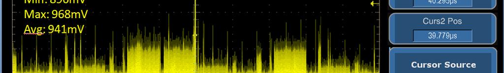
14 Results Long term noise = (max:max min:min) If statistics are enabled then use the maximum max and the minimum min values and not the mean values Check these values with cursors on the persistence image Measurement we need is therefore the highest h level l attained and the lowest level attained
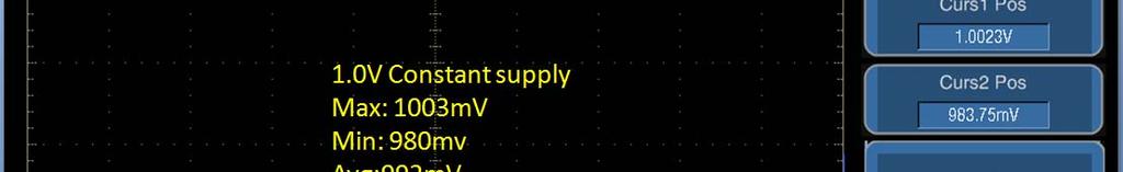
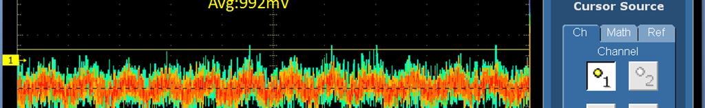
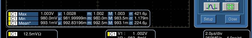
15 Example measurements Maximum max and minimum min measurements
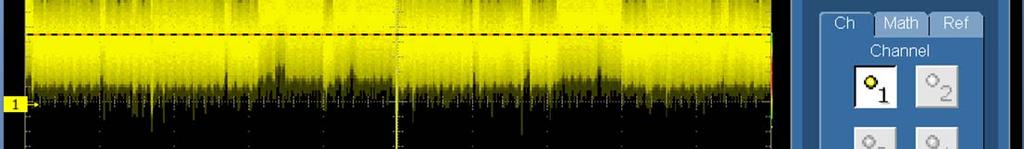
16 Example measurements Lots of issues


17 Example measurements 360KHz switcher noise should be fairly simple to control with correct switcher component selection
Probe Considerations for Low Voltage Measurements such as Ripple
 Probe Considerations for Low Voltage Measurements such as Ripple Our thanks to Tektronix for allowing us to reprint the following article. Figure 1. 2X Probe (CH1) and 10X Probe (CH2) Lowest System Vertical
Understanding, measuring, and reducing output noise in DC/DC switching regulators
 Understanding, measuring, and reducing output noise in DC/DC switching regulators Practical tips for output noise reduction Katelyn Wiggenhorn, Applications Engineer, Buck Switching Regulators Robert Blattner,
AC Measurements with the Agilent 54622D Oscilloscope
 AC Measurements with the Agilent 54622D Oscilloscope Objectives: At the end of this experiment you will be able to do the following: 1. Correctly configure the 54622D for measurement of voltages. 2. Perform
Measuring Power Supply Switching Loss with an Oscilloscope
 Measuring Power Supply Switching Loss with an Oscilloscope Our thanks to Tektronix for allowing us to reprint the following. Ideally, the switching device is either on or off like a light switch, and instantaneously
TAKE THE MYSTERY OUT OF PROBING. 7 Common Oscilloscope Probing Pitfalls to Avoid
 TAKE THE MYSTERY OUT OF PROBING 7 Common Oscilloscope Probing Pitfalls to Avoid Introduction Understanding common probing pitfalls and how to avoid them is crucial in making better measurements. In an
Decoupling capacitor placement
 Decoupling capacitor placement Covered in this topic: Introduction Which locations need decoupling caps? IC decoupling Capacitor lumped model How to maximize the effectiveness of a decoupling cap Parallel
The Inductance Loop Power Distribution in the Semiconductor Test Interface. Jason Mroczkowski Multitest
 The Inductance Loop Power Distribution in the Semiconductor Test Interface Jason Mroczkowski Multitest j.mroczkowski@multitest.com Silicon Valley Test Conference 2010 1 Agenda Introduction to Power Delivery
SiTime University Turbo Seminar Series
 SiTime University Turbo Seminar Series How to Measure Clock Jitter Part I Principle and Practice April 8-9, 2013 Agenda Jitter definitions and terminology Who cares about jitter How to measure clock jitter
Power Distribution Network Design for Stratix IV GX and Arria II GX FPGAs
 Power Distribution Network Design for Stratix IV GX and Arria II GX FPGAs Transceiver Portfolio Workshops 2009 Question What is Your PDN Design Methodology? Easy Complex Historical Full SPICE simulation
Description. This Clock Multiplier is the most cost-effective way to Input crystal frequency of 5-40 MHz
 PT7C4512 Features Description Zero ppm multiplication error This Clock Multiplier is the most cost-effective way to Input crystal frequency of 5-40 MHz generate a high quality, high frequency clock outputs
QUICK START GUIDE FOR DEMONSTRATION CIRCUIT 781 HIGH EFFICIENCY SYNCHRONOUS NONISOLATED FLYBACK
 DESCRIPTION QUICK START GUIDE FOR DEMONSTRATION CIRCUIT 781 LTC3803ES6 Demonstration circuit 781 is a Telecom DC/DC converter featuring the LTC3803ES6 constant frequency current mode flyback controller.
EUP V/12V Synchronous Buck PWM Controller DESCRIPTION FEATURES APPLICATIONS. Typical Application Circuit. 1
 5V/12V Synchronous Buck PWM Controller DESCRIPTION The is a high efficiency, fixed 300kHz frequency, voltage mode, synchronous PWM controller. The device drives two low cost N-channel MOSFETs and is designed
SR A, 30V, 420KHz Step-Down Converter DESCRIPTION FEATURES APPLICATIONS TYPICAL APPLICATION
 SR2026 5A, 30V, 420KHz Step-Down Converter DESCRIPTION The SR2026 is a monolithic step-down switch mode converter with a built in internal power MOSFET. It achieves 5A continuous output current over a
LeCroy 9304A, 9304AM Digital Oscilloscopes 200 MHz Bandwidth, 100 MS/s. Main Features
 LeCroy 9304A, 9304AM Digital Oscilloscopes 200 MHz Bandwidth, 100 MS/s Main Features Four Channels 50k and 200k Point Records DOS Compatible Floppy Disk, PCMCIA portable hard drive and Memory Card Options
Circuit Layout Techniques And Tips (Part III of VI) by Bonnie C. Baker and Ezana Haile, Microchip Technology Inc.
 by Bonnie C. Baker and Ezana Haile, Microchip Technology Inc.") Circuit Layout Techniques And Tips (Part III of VI) by Bonnie C. Baker and Ezana Haile, Microchip Technology Inc. The major classes of parasitic generated by the PC board layout come in the form of resistors,
Circuit Layout Techniques And Tips (Part III of VI) by Bonnie C. Baker and Ezana Haile, Microchip Technology Inc. The major classes of parasitic generated by the PC board layout come in the form of resistors,
Current Probe. Inspector Data Sheet. Low-noise, high quality measurement signal for side channel acquisition on embedded devices.
 Inspector Data Sheet Low-noise, high quality measurement signal for side channel acquisition on embedded devices. Riscure Version 1c.1 1/5 Introduction Measuring the power consumption of embedded technology
Features. = +25 C, 50 Ohm System, Vcc= 5V
 Typical Applications Prescaler for 1 MHz to 13 GHz PLL Applications: Point-to-Point / Multi-Point Radios VSAT Radios Fiber Optic Test Equipment Space & Military Functional Diagram Features Ultra Low ssb
Application Guidelines for Non-Isolated Converters AN Input Filtering for Austin Lynx Series POL Modules
 PDF Name: input_filtering_an.pdf Application Guidelines for Non-Isolated Converters AN4-2 Introduction The Austin Lynx TM and Lynx II family of non-isolated POL (point-of-load) modules use the buck converter
U1571A Ni-MH Battery Pack for U1600A Handheld Oscilloscopes
 United States Home >... > Oscilloscope Accessories > U1600 Series Oscilloscope Accessories > U1571A Ni-MH Battery Pack for U1600A Handheld Oscilloscopes Key Specifications Features Ni-MH Battery Pack,
Quick guide to Power. V1.2.1 July 29 th 2013
 Quick guide to Power Distribution ib ti Network Design V1.2.1 July 29 th 2013 High level High current, high transient Power Distribution Networks (PDN) need to be able to respond to changes and transients
ME 365 EXPERIMENT 1 FAMILIARIZATION WITH COMMONLY USED INSTRUMENTATION
 Objectives: ME 365 EXPERIMENT 1 FAMILIARIZATION WITH COMMONLY USED INSTRUMENTATION The primary goal of this laboratory is to study the operation and limitations of several commonly used pieces of instrumentation:
Divide. MHz models) waveform record
 waveform record") The 2550 series digital storage oscilloscopes provide high performance and value in 2-channel and 4-channel configurations. With bandwidth from 70 MHz to 300 MHz and 2 GSa/s sample rates, these oscilloscopes
The 2550 series digital storage oscilloscopes provide high performance and value in 2-channel and 4-channel configurations. With bandwidth from 70 MHz to 300 MHz and 2 GSa/s sample rates, these oscilloscopes
Guide Version Five techniques for fast, accurate power integrity measurements
 Guide Version 01.00 Five techniques for fast, accurate power integrity measurements Rail voltages are getting smaller, and tolerances are decreasing. As a result, making accurate power rail measurements
MIL-STD-883E METHOD 3024 SIMULTANEOUS SWITCHING NOISE MEASUREMENTS FOR DIGITAL MICROELECTRONIC DEVICES
 SIMULTANEOUS SWITCHING NOISE MEASUREMENTS FOR DIGITAL MICROELECTRONIC DEVICES 1. Purpose. This method establishes the procedure for measuring the ground bounce (and V CC bounce) noise in digital microelectronic
SAMPLE: EXPERIMENT 2 Series RLC Circuit / Bode Plot
 SAMPLE: EXPERIMENT 2 Series RLC Circuit / Bode Plot ---------------------------------------------------------------------------------------------------- This experiment is an excerpt from: Electric Experiments
LABORATORY 4. Palomar College ENGR210 Spring 2017 ASSIGNED: 3/21/17
 LABORATORY 4 ASSIGNED: 3/21/17 OBJECTIVE: The purpose of this lab is to evaluate the transient and steady-state circuit response of first order and second order circuits. MINIMUM EQUIPMENT LIST: You will
PI6C49X0204A. Low Skew 1 TO 4 Clock Buffer. Features. Description. Block Diagram. Pin Assignment
 Features ÎÎLow skew outputs (250 ps) ÎÎPackaged in 8-pin SOIC ÎÎLow power CMOS technology ÎÎOperating Voltages of 1.5 V to 3.3 V ÎÎOutput Enable pin tri-states outputs ÎÎ3.6 V tolerant input clock ÎÎIndustrial
PT7C4502 PLL Clock Multiplier
 Features Low cost frequency multiplier Zero ppm multiplication error Input crystal frequency of 5-30 MHz Input clock frequency of 4-50 MHz Output clock frequencies up to 180 MHz Period jitter 50ps (100~180MHz)
PDN Probes. P2100A/P2101A Data Sheet. 1-Port and 2-Port 50 ohm Passive Probes
 P2100A/P2101A Data Sheet PDN Probes 1-Port and 2-Port 50 ohm Passive Probes power integrity PDN impedance testing ripple PCB resonances transient step load stability and NISM noise TDT/TDR clock jitter
University of Jordan School of Engineering Electrical Engineering Department. EE 204 Electrical Engineering Lab
 University of Jordan School of Engineering Electrical Engineering Department EE 204 Electrical Engineering Lab EXPERIMENT 1 MEASUREMENT DEVICES Prepared by: Prof. Mohammed Hawa EXPERIMENT 1 MEASUREMENT
B. Equipment. Advanced Lab
 Advanced Lab Measuring Periodic Signals Using a Digital Oscilloscope A. Introduction and Background We will use a digital oscilloscope to characterize several different periodic voltage signals. We will
PT7C4511. PLL Clock Multiplier. Features. Description. Pin Configuration. Pin Description
 Features Zero ppm multiplication error Input crystal frequency of 5-30 MHz Input clock frequency of - 50 MHz Output clock frequencies up to 200 MHz Peak to Peak Jitter less than 200ps over 200ns interval
High Speed Digital Design & Verification Seminar. Measurement fundamentals
 High Speed Digital Design & Verification Seminar Measurement fundamentals Agenda Sources of Jitter, how to measure and why Importance of Noise Select the right probes! Capture the eye diagram Why measure
PI3USB102 PI3USB102 Demo Board Rev.A User Manual
 PI3USB102 PI3USB102 Demo Board Rev.A User Manual Introduction This user manual describes the components and operation of the PI3USB102 Demo Board. USB2.0 high-speed, fullspeed and low speed signal quality
AC Magnitude and Phase
 AC Magnitude and Phase Objectives: oday's experiment provides practical experience with the meaning of magnitude and phase in a linear circuits and the use of phasor algebra to predict the response of
Lab Equipment EECS 311 Fall 2009
 Lab Equipment EECS 311 Fall 2009 Contents Lab Equipment Overview pg. 1 Lab Components.. pg. 4 Probe Compensation... pg. 8 Finite Instrumentation Impedance. pg.10 Simulation Tools..... pg. 10 1 - Laboratory
PART MAX2605EUT-T MAX2606EUT-T MAX2607EUT-T MAX2608EUT-T MAX2609EUT-T TOP VIEW IND GND. Maxim Integrated Products 1
 19-1673; Rev 0a; 4/02 EVALUATION KIT MANUAL AVAILABLE 45MHz to 650MHz, Integrated IF General Description The are compact, high-performance intermediate-frequency (IF) voltage-controlled oscillators (VCOs)
Experiment 1.A. Working with Lab Equipment. ECEN 2270 Electronics Design Laboratory 1
 .A Working with Lab Equipment Electronics Design Laboratory 1 1.A.0 1.A.1 3 1.A.4 Procedures Turn in your Pre Lab before doing anything else Setup the lab waveform generator to output desired test waveforms,
EE431 Lab 1 Operational Amplifiers
 Feb. 10, 2015 Report all measured data and show all calculations Introduction The purpose of this laboratory exercise is for the student to gain experience with measuring and observing the effects of common
U1604A Handheld Oscilloscopes, 40 MHz
 Products & Services Technical Support Buy Industries About Agilent Search: All Test & Measurement Go United States Home >... > Oscilloscopes > U1600A Series handheld oscilloscopes (2 models) > U1604A Handheld
ET1210: Module 5 Inductance and Resonance
 Part 1 Inductors Theory: When current flows through a coil of wire, a magnetic field is created around the wire. This electromagnetic field accompanies any moving electric charge and is proportional to
ECE 6416 Low-Noise Electronics Orientation Experiment
 ECE 6416 Low-Noise Electronics Orientation Experiment Object The object of this experiment is to become familiar with the instruments used in the low noise laboratory. Parts The following parts are required
MP A, 30V, 420kHz Step-Down Converter
 The Future of Analog IC Technology DESCRIPTION The MP28490 is a monolithic step-down switch mode converter with a built in internal power MOSFET. It achieves 5A continuous output current over a wide input
Sirindhorn International Institute of Technology Thammasat University
 Sirindhorn International Institute of Technology Thammasat University School of Information, Computer and Communication Technology COURSE : ECS 34 Basic Electrical Engineering Lab INSTRUCTOR : Dr. Prapun
332:223 Principles of Electrical Engineering I Laboratory Experiment #2 Title: Function Generators and Oscilloscopes Suggested Equipment:
 RUTGERS UNIVERSITY The State University of New Jersey School of Engineering Department Of Electrical and Computer Engineering 332:223 Principles of Electrical Engineering I Laboratory Experiment #2 Title:
LoadSlammer User Guide LS50 and LS1000
 LoadSlammer User Guide LS50 and LS1000 1 CONTENTS 2 Introduction... 2 2.1 Overview... 2 2.2 Hardware... 2 2.3 Specifications LS50... 3 2.4 Specifications LS1000... 4 3... 5 3.1 Physical Connection to DUT...
LOCO PLL CLOCK MULTIPLIER. Features
 DATASHEET ICS501A Description The ICS501A LOCO TM is the most cost effective way to generate a high quality, high frequency clock output from a lower frequency crystal or clock input. The name LOCO stands
AT V,3A Synchronous Buck Converter
 FEATURES DESCRIPTION Wide 8V to 40V Operating Input Range Integrated 140mΩ Power MOSFET Switches Output Adjustable from 1V to 25V Up to 93% Efficiency Internal Soft-Start Stable with Low ESR Ceramic Output
Three-Channel, 5th Order, Standard Definition Video Filter Driver BL1513
 Three-Channel, 5th Order, Standard Definition Video Filter Driver Description The is a low-voltage, three-channel video amplifier with integrated reconstruction and s. Specially suited for standard definition
The Tuned Circuit. Aim of the experiment. Circuit. Equipment and components. Display of a decaying oscillation. Dependence of L, C and R.
 The Tuned Circuit Aim of the experiment Display of a decaying oscillation. Dependence of L, C and R. Circuit Equipment and components 1 Rastered socket panel 1 Resistor R 1 = 10 Ω, 1 Resistor R 2 = 1 kω
Effect of Power Noise on Multi-Gigabit Serial Links
 Effect of Power Noise on Multi-Gigabit Serial Links Ken Willis (kwillis@sigrity.com) Kumar Keshavan (ckumar@sigrity.com) Jack Lin (jackwclin@sigrity.com) Tariq Abou-Jeyab (tariqa@sigrity.com) Sigrity Inc.,
1Gsps Dual-Stage Differential Track-and-Hold TH721
 1Gsps Dual-Stage Differential Track-and-Hold TH721 PRODUCT DESCRIPTION TH721 is a dual-stage differential Track-and-Hold amplifier with independent clock inputs. TH721 is able to sample 1 GHz signal with
Power Plane and Decoupling Optimization. Isaac Waldron
 Power Plane and Decoupling Optimization p Isaac Waldron Overview Frequency- and time-domain power distribution system specifications Decoupling design example Bare board Added d capacitors Buried Capacitance
AS SERIES (2.00 x 1.6 Package) Up to 20 Watt DC-DC Converter
 Up to 20 Watt DC-DC Converter") PRODUCT OVERVIEW The AS series offer up to 20 watts of output power in standard 2.00 x 1.60 x 0.45 inches packages. This series features high efficiency and 1500 Volts of DC isolation. The AS series provides
PRODUCT OVERVIEW The AS series offer up to 20 watts of output power in standard 2.00 x 1.60 x 0.45 inches packages. This series features high efficiency and 1500 Volts of DC isolation. The AS series provides
Liteon Semiconductor Corporation LSP3308A 6 Channels LED Boost Driver
 FEATURES Six Constant-Current Output Channels (Io=40mA each @ Vin=12V; Io=30mA each @ Vin=5V;) Parallel Channels Allow Higher Current per LED String Maximum 40V Continuous Voltage Output Limit for Each
How to Setup a Real-time Oscilloscope to Measure Jitter
 TECHNICAL NOTE How to Setup a Real-time Oscilloscope to Measure Jitter by Gary Giust, PhD NOTE-3, Version 1 (February 16, 2016) Table of Contents Table of Contents... 1 Introduction... 2 Step 1 - Initialize
Application Note 5525
 Using the Wafer Scale Packaged Detector in 2 to 6 GHz Applications Application Note 5525 Introduction The is a broadband directional coupler with integrated temperature compensated detector designed for
PI3DPX1207B Layout Guideline. Table of Contents. 1 Layout Design Guideline Power and GROUND High-speed Signal Routing...
 PI3DPX1207B Layout Guideline Table of Contents 1 Layout Design Guideline... 2 1.1 Power and GROUND... 2 1.2 High-speed Signal Routing... 3 2 PI3DPX1207B EVB layout... 8 3 Related Reference... 8 Page 1
CS101. Conducted Susceptibility CS101. CS101 Maximum Current. CS101 Limits. Basis For CS101 Limits. Comparison To MIL-STD Vdc or Less
 Conducted Susceptibility CS1 Raymond K. Adams Fischer Custom Communications, Inc. 20603 Earl Street Torrance, CA 90503 (3)303-3300 radams@fischercc.com CS1 Applicability DC and AC Input Power Leads Does
Single-Channel, 5th Order, Standard Definition Video Filter Driver BL1511B
 Single-Channel, 5th Order, Standard Definition Video Filter Driver Description The is a low-voltage, single-channel video amplifier with integrated reconstruction filter and input clamps. Specially suited
Data Acquisition Board HERALD Design Manual
 Data Acquisition Board Design Manual Version: A 2006-08-28 Prepared By: Name(s) and Signature(s) Organization NRAO NRAO Approved By: Name and Signature Organization Released By: Name and Signature Organization
S020_084-S V input, 1.2 to 5.0V adjustable output, 20A or 55W
 S2_84-S2- Features High output 2A up to 55W max 12V +5/-1% input Load Regulation ±.5% Factory set to 1.2V output with output trim up to 5.V High Efficiency to 93% Power Good and Enable Short Circuit protection
MP2482 5A, 30V, 420kHz Step-Down Converter
 The Future of Analog IC Technology DESCRIPTION The MP2482 is a monolithic step-down switch mode converter with a built in internal power MOSFET. It achieves 5A continuous output current over a wide input
Decoupling capacitor uses and selection
 Decoupling capacitor uses and selection Proper Decoupling Poor Decoupling Introduction Covered in this topic: 3 different uses of decoupling capacitors Why we need decoupling capacitors Power supply rail
DS 6000 Specifications
 DS 6000 Specifications All the specifications are guaranteed except the parameters marked with Typical and the oscilloscope needs to operate for more than 30 minutes under the specified operation temperature.
Antenna Matching Within an Enclosure Part II: Practical Techniques and Guidelines
 Antenna Matching Within an Enclosure Part II: Practical Techniques and Guidelines By Johnny Lienau, RF Engineer June 2012 Antenna selection and placement can be a difficult task, and the challenges of
Agilent Technologies 3000 Series Oscilloscopes
 Agilent Technologies 3000 Series Oscilloscopes Data Sheet The performance and features you need at the industry s lowest price Features: 60 to 200 MHz bandwidths 1 GSa/s maximum sample rate Large 15-cm
Tektronix MDO3000 Series Oscilloscope. Demonstration Guide
 Tektronix MDO3000 Series Oscilloscope 2 www.tektronix.com/mdo3000 Table of Contents Tektronix MDO3000 Series Oscilloscope... 4 About This Guide... 6 Powering on the Board... 8 MDO3000 Series Front Panel
RTH GHz Bandwidth High Linearity Track-and-Hold REV-DATE PA FILE DS_0162PA2-3215
 RTH090 25 GHz Bandwidth High Linearity Track-and-Hold REV-DATE PA2-3215 FILE DS RTH090 25 GHz Bandwidth High Linearity Track-and-Hold Features 25 GHz Input Bandwidth Better than -40dBc THD Over the Total
PowerAmp Design. PowerAmp Design PAD183 COMPACT HIGH VOLTAGE OP AMP
 PowerAmp Design Rev B KEY FEATURES LOW COST SMALL SIZE 40mm SQUARE HIGH VOLTAGE 350 VOLTS HIGH OUTPUT CURRENT 1.5A 35 WATT DISSIPATION CAPABILITY 100kHz POWER BANDWIDTH 330Vp-p 100V/µS SLEW RATE APPLICATIONS
AN1995 Evaluating the SA605 SO and SSOP demo-board
 RF COMMUNICATIONS PRODUCTS Evaluating the SA605 SO and SSOP demo-board Alvin K. Wong 997 Oct 9 Philips Semiconductors Author: Alvin K. Wong INTRODUCTION With the increasing demand for smaller and lighter
Agilent Technologies 3000 Series Oscilloscopes
 Agilent Technologies 3000 Series Oscilloscopes Data Sheet Full-featured oscilloscopes for the smallest budgets Features: 60 to 200 MHz bandwidths 1 GSa/s maximum sample rate Large 15-cm (5.7-in) color
2-channel models. 4-channel models
 2-channel models DSO1052B DSO1072B DSO1102B DSO1152B 50 MHz 70 MHz 100 MHz 150 MHz 4-channel models DSO1004A DSO1014A DSO1024A 60 MHz 100 MHz 200 MHz DSO1022A 200 MHz Segment 1 Segment 2 Segment 1000
EN A Voltage Mode Synchronous Buck PWM DC-DC Converter with Integrated Inductor RoHS Compliant July Features. Description.
 EN5330 3A Voltage Mode Synchronous Buck PWM DC-DC Converter with Integrated Inductor RoHS Compliant July 2007 Description The EN5330 is a Power System on a Chip DC- DC converter. It is specifically designed
IsoVu Optically Isolated DC - 1 GHz Measurement System Offers >120 db CMRR with 2kV Common Mode Range
 IsoVu Optically Isolated DC - 1 GHz Measurement System Offers >120 db CMRR with 2kV Common Mode Range Introduction This white paper describes the optically isolated measurement system architecture trademarked
PowerAmp Design. PowerAmp Design PAD112 HIGH VOLTAGE OPERATIONAL AMPLIFIER
 PowerAmp Design Rev C KEY FEATURES LOW COST HIGH VOLTAGE 150 VOLTS HIGH OUTPUT CURRENT 5 AMPS 50 WATT DISSIPATION CAPABILITY 100 WATT OUTPUT CAPABILITY INTEGRATED HEAT SINK AND FAN COMPATIBLE WITH PAD123
PRODUCT OVERVIEW. APPLICATIONS: Distributed Power Architectures Mobile telecommunication Industrial applications Battery operated equipment
 FEATURES Industry Standard 24-Pin DIP package 15Watts Isolated Output 4:1 Input Range Regulated Outputs Up to 90 % Efficiency Low No Load Power Consumption -40 C to +85 C industrial temperature range Negative
Revised PSE and PD Ripple Limits. Andy Gardner
 Revised PSE and PD Ripple Limits Andy Gardner Presentation Objectives To propose revised limits for PSE ripple voltage and PD ripple current required to ensure data integrity of the PHYs in response to
LM2462 Monolithic Triple 3 ns CRT Driver
 LM2462 Monolithic Triple 3 ns CRT Driver General Description The LM2462 is an integrated high voltage CRT driver circuit designed for use in color monitor applications. The IC contains three high input
Uncle Sparky s Guide to Voltage, Current, and Resistance Measurements. Spring 2014
 Uncle Sparky s Guide to Voltage, Current, and Resistance Measurements Spring 2014 The most important quantities in a circuit system are voltage and current. These include both AC and DC voltages and currents.
FlexRay Communications System. Physical Layer Common mode Choke EMC Evaluation Specification. Version 2.1
 FlexRay Communications System Physical Layer Common mode Choke EMC Evaluation Specification Version 2.1 Disclaimer DISCLAIMER This specification as released by the FlexRay Consortium is intended for the
S24SE/S24DE series 30W Single/Dual Output DC/DC Converter
 FEATURES Efficiency up to 89% Wide input range, 9V-36V Package with Industry Standard Pinout Package Dimension: 25.4 x25.4 x10.2mm (1.0 x1.0 x0.40 )(No HSK) Over voltage protection, hiccup mode Over current
Best Design and Layout Practices for SiTime Oscillators
 March 17, 2016 Best Design and Layout Practices 1 Introduction... 1 2 Decoupling... 1 3 Bypassing... 4 4 Power Supply Noise Reduction... 5 5 Power Supply Management... 6 6 Layout Recommendations for SiTime
PARAMETER CONDITION VALUE Minimum Input Voltage. Maximum Input Voltage. Maximum Output Current for 3.3Voutput. Maximum Output Current for 2.
 ECRIPTION QUICK TART UIE FOR EMONTRATION CIRCUIT 541A LTC3723-1, LTC3901, LT3710 and LT1431 emonstration circuit 541A is an isolated synchronous push-pull converter featuring the LTC3723-1, LTC3901, LT1431
Evaluate: MAX2828/MAX2829. MAX2828/MAX2829 Evaluation Kits. General Description. Features. Quick Start. Connections and Setup. Test Equipment Required
 MAX2828/MAX2829 Evaluation Kits Evaluate: MAX2828/MAX2829 General Description The MAX2828/MAX2829 evaluation kits (EV kits) simplify the testing of the MAX2828/MAX2829. The EV kits provide 50Ω SMA connectors
Course Introduction. Content 15 pages. Learning Time 30 minutes
 Course Introduction Purpose This course discusses techniques for analyzing and eliminating noise in microcontroller (MCU) and microprocessor (MPU) based embedded systems. Objectives Learn about how packaging
AC/DC Power Supply Series APPLICATION NOTE
 ZMS100 AC/DC Power Supply Series APPLICATION NOTE ZMS100 Application Notes Issue 3 Document Number 260160 Page 1 of 15 Contents Contents... 2 1. INPUT... 3 AC INPUT LINE REQUIREMENTS... 3 2. DC OUTPUT...
PowerAmp Design. PowerAmp Design PAD135 COMPACT HIGH VOLATGE OP AMP
 PowerAmp Design COMPACT HIGH VOLTAGE OP AMP Rev G KEY FEATURES LOW COST SMALL SIZE 40mm SQUARE HIGH VOLTAGE 200 VOLTS HIGH OUTPUT CURRENT 10A PEAK 40 WATT DISSIPATION CAPABILITY 200V/µS SLEW RATE APPLICATIONS
S24SE/S24DE series 30W Single/Dual Output DC/DC Converter
 Model List Model Number Input Voltage Output Voltage Output Current Input Current (typ input voltage) (Range) Max. Min. @Max. Load @No Load Load Regulation Maxcapacitive Efficiency Load (typ.) @Max. Load
Measuring Power Supply Switching Loss with an Oscilloscope
 Measuring Power Supply Switching Loss with an Oscilloscope Application Note Introduction With the demand for improving power efficiency and extending the operating time of battery-powered devices, the
RS Pro HANDY OSCILLOSCOPE RSHS800 SERIES
 Product Datasheet ENGLISH Stock No: 1236454 1236455 1236456 1236457 RS Pro HANDY OSCILLOSCOPE RSHS800 SERIES Application Domain Outdoor measure Circuit measure Wind power, PV power and other new energy
T est POST OFFICE BOX 1927 CUPERTINO, CA TEL E P H ONE (408) FAX (408) ARIES ELECTRONICS
 FAX (408) ARIES ELECTRONICS") G iga T est L abs POST OFFICE BOX 1927 CUPERTINO, CA 95015 TEL E P H ONE (408) 524-2700 FAX (408) 524-2777 ARIES ELECTRONICS BGA SOCKET (0.80MM TEST CENTER PROBE CONTACT) Final Report Electrical Characterization
G iga T est L abs POST OFFICE BOX 1927 CUPERTINO, CA 95015 TEL E P H ONE (408) 524-2700 FAX (408) 524-2777 ARIES ELECTRONICS BGA SOCKET (0.80MM TEST CENTER PROBE CONTACT) Final Report Electrical Characterization
RS Pro HANDY OSCILLOSCOPE RSHS800 SERIES
 Product Datasheet ENGLISH Stock No: 1236454 1236455 1236456 1236457 RS Pro HANDY OSCILLOSCOPE RSHS800 SERIES Application Domain Outdoor measure Circuit measure Wind power, PV power and other new energy
DIO6010 High-Efficiency 1.5MHz, 1A Continuous, 1.5A Peak Output Synchronous Step Down Converter
 DIO6010 High-Efficiency 1.5MHz, 1A Continuous, 1.5A Peak Output Synchronous Step Down Converter Rev 1.2 Features Low R DS(ON) for internal switches (top/bottom) 230mΩ/170mΩ, 1.0A 2.5-5.5V input voltage
Features. = +25 C, 50 Ohm System, Vcc= +5V
 v5.1211 Typical Applications Prescaler for DC to 18 GHz PLL Applications: Point-to-Point / Multi-Point Radios VSAT Radios Fiber Optic Test Equipment Military Functional Diagram Features Ultra Low ssb Phase
LVDS Owner s Manual. A General Design Guide for National s Low Voltage Differential Signaling (LVDS) Products. Moving Info with LVDS
 Products. Moving Info with LVDS") LVDS Owner s Manual A General Design Guide for National s Low Voltage Differential Signaling (LVDS) Products Moving Info with LVDS Revision 2.0 January 2000 LVDS Evaluation Boards Chapter 6 6.0.0 LVDS
LVDS Owner s Manual A General Design Guide for National s Low Voltage Differential Signaling (LVDS) Products Moving Info with LVDS Revision 2.0 January 2000 LVDS Evaluation Boards Chapter 6 6.0.0 LVDS
EOS Exposure of Components in Soldering Process
 EOS Exposure of Components in Soldering Process Published in EEWeb By Vladimir Kraz, ONFilter, 2 May 2012 Soldering irons, solder extractors and other equipment that comes in direct electrical contact
ML12561 Crystal Oscillator
 ML56 Crystal Oscillator Legacy Device: Motorola MC56 The ML56 is the military temperature version of the commercial ML06 device. It is for use with an external crystal to form a crystal controlled oscillator.
Transimpedance Amplifier with 100mA Input Current Clamp for LiDAR Applications
 EVALUATION KIT AVAILABLE MAX4658/MAX4659 Transimpedance Amplifier with 1mA Input General Description The MAX4658 and MAX4659 are transimpedance amplifiers for optical distance measurement receivers for
QUICK START GUIDE FOR DEMONSTRATION CIRCUIT 1231A DUAL OUTPUT, DUAL PHASE 5A SYNCHRONOUS BUCK CONVERTER
 DESCRIPTION QUICK START GUIDE FOR DEMONSTRATION CIRCUIT 1231A LTC3850EGN Demonstration circuit 1231A is a Dual Output, Dual Phase 5A Synchronous Buck Converter featuring the LTC3850EGN. The entire circuit,