Class E/F Amplifiers
|
|
|
- Arnold May
- 6 years ago
- Views:
Transcription

1 Class E/F Amplifiers

2 Normalized Output Power It s easy to show that for Class A/B/C amplifiers, the efficiency and output power are given by: It s useful to normalize the output power versus the product of V bk and I max (I dc )

3 Class A/B/C As efficiency improves, the normalized output power drops from ~10% down to 0%
4 Class A/B/C Properties Keep voltage waveform sinusoidal amplitude is limited to V dd /2 Only way to improve efficiency is to control current Require very large on current to deliver power

5 Class F Start with Class B current waveform only odd harmonics Tune impedance at odd harmonics to be an open circuit to dissipate no harmonic power but allow odd harmonics in voltage waveform Tune even harmonics to short circuit to avoid dissipating power

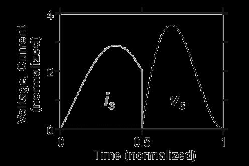
6 Class F Waveforms Maximally flat Class F waveforms. An ideal Class F amplifier has a square voltage waveform and 100% efficiency.

7 Class F Efficiency In theory, if you can control an infinite number of harmonics, efficiency approaches 100%

8 Class F Output Power Square wave has a peak fundamental 4/π larger than the peak 1 db output power enhancement
9 Class F Disadvantages Output capacitance of device not naturally absorbed into network need inductor to tune it out Difficult to control more than 5 th harmonic resonators are lossy and additional losses present diminishing returns on efficiency.

10 Switching Amplifiers Operate transistor in triode region where it acts like a switch. For an ideal switch the power dissipated in the switch is zero, right? Are all switching PA s the same?
 system. The design of the output network completely determines the behavior of the circuit.")
11 Linear Time-Varying Systems Even though transistor is non-linear, the operation of the periodic switching action can be modeled as a linear time-varying (periodic) system. The design of the output network completely determines the behavior of the circuit.
12 I-V Solution for Swithing Amps ( θ D) ( v s = 0) ( θ D) ( i s = 0) For trans-conductance amplifiers, the current is known, so the voltage is determined by the load network. In a switching amplifier, when the switch is on, the voltage is forced to zero, and the current through the switch can take on any value. Likewise, when the switch is off, the switch current is zero, but the voltage can take on any value
13 Impedance at Harmonics v s ( θ) = V DC + v k cos( kθ + α k ) k = 1 i s ( θ) = I DC + i k cos( kθ+ β k ) ( )e j α k β k v k i k k ( ) = { 1, 2, 3, 4, } Z in ( k) k = 1 α β The waveform shape, therefore, is completely determined by the load network impedance (it s a linear system viewed from this perspective)
14 Inverse Class of Operation By duality, any PA can be transformed into it s dual (where the role of current/voltage are switched) by imposing the complementary admittance condition For instance a Class D voltage switching amplifier can be transformed into a current switching amp i s ( θ) = I DC + i k cos( kθ+ α k ) k = 1 v s ( θ) = V DC + v k cos( kθ + β k ) i k k = 1 ( θ D) ( i s = 0) ( θ D) ( v s = 0) ( )e j α k β k v k k ( ) = { 1, 2, 3, 4, } Y in ( k)

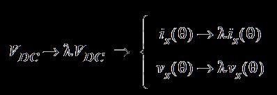
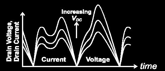
15 Bias Scaling Scaling supply changes voltage/current waveforms by the same scale factor.

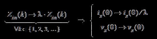

16 Impedance Scaling

17 Switch Losses When a switch is closed across a capacitor, an impulse of current flows through the switch to discharge the capacitor. The energy stored in the capacitor is dissipated into heat through the switch. (ideal switch?) If you make a smaller switch, the on-resistance goes down so you have to live with finite capacitance.
")
18 ZVS A ZVS network will return the voltage to zero at the moment of switch turn-on. To make the circuit more robust, the derivative of the voltage can also be forced to zero (or n- derivatives ) to obtain a maximally flat zero.
19 Switch Losses: ZCS Condition The dual of ZVS is ZCS. What happens if you open circuit an inductor with current (flux)? The energy stored in the magnetic flux is dissipated In practice the voltage kick produced by the inductor will break down the switch and conduct current. It s also possible to design a load network that returns the current to zero just before the switch opens.


20 Switching Inductors If the inductor is large enough, it s switching behavior can be idealized.

21 Class D Two switches used to realize square waveform. Series tank only allows fundamental current to flow into load. Switch capacitance limits efficiency in high frequency applications.


22 Class D -1 The Dual Class D amplifier (interchange voltage/current square wave current, sinusoidal voltage, parallel LCR filter) Chokes act like current sources. ZVS by design but only if there is no device capacitance to begin with.

23 Class E Switch driven with 50% duty cycle. Device capacitance C s absorbed into network. The current i 1 is sinusoidal and the current through the choke is DC. The sum of these currents flows through the switch + capacitor.

24 Class E Currents When switch is closed, all the current flows through it. When open, this same current must flow through the capacitor. The voltage across the capacitor is given by the integral of the current since
.")
25 Class E Voltages We can impose voltage continuity, so θ=π. But we have two degrees of freedom, so we can also set the derivative of the voltage to zero (ZdVS). When both conditions are satisfied, we have a class E amplifier.
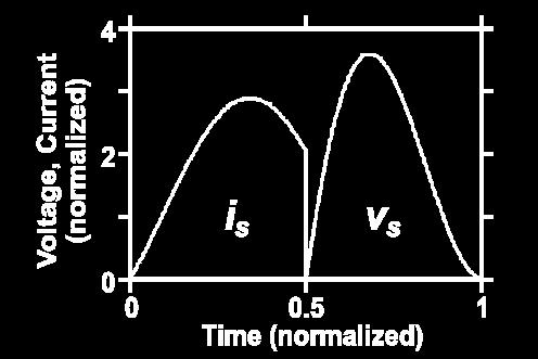
26 Class E Current/Voltage ZVS & ZdVS
27 Class E Load & Swing The load is given from Fourier analysis of the current/ voltage. To realize a Class E amplifier requires an inductive load. One big disadvantage of the Class E amplifier is that the voltage swing across the device is very large (nearly 4 V DD ).


28 Switching Amplifier Efficiency For ZVS, P sw is zero

29 Switching Amplifier PAE This result includes the gain of the amplifier. To arrive at the final result, we assume 100% drain efficiency and ZVS. Note that P in is a function of the transistor size.
 on the device.")
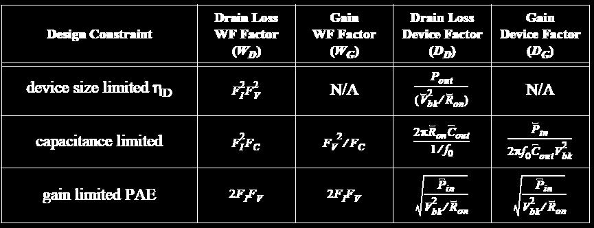
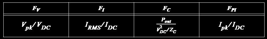
30 Switch FOM It s useful to relate the effiency to peak current/voltage swings (stress) on the device. For a high efficiency PA we have

31 FOM (cont) Peak voltage versus DC Peak current versus DC RMS current versus DC Output power versus peak stress on transsitor Output power versus stored reactive power. The smaller this ratio, the more the design can tolerate output capacitance, and hence a larger transistor with lower conductive losses.


32 η D 1 Device Size Limited Maximum Drain Efficiency 2 I RMS R on V DC I DC All terms except the third are invariant and only depend on the tuning strategy. Minimize the third term by using the highest peak voltage possible (minimize current through device).
 and only")

33 Capacitance Limited Drain Efficiency η D 1 2 I RMS R on V DC I DC Increase device size until the switch output capacitance equals the total output capacitance All terms except the last are invariant (bias, impedance scaling) and only depend on the switching network. Note the third term depends on technology but is independent of transistor size. Voltage waveform properties do not come into play. To minimize the final term, maximize C out. Final efficiency only depends on technology RC time constant:
34 Reactive Energy Term The second term needs further explanation: 2 V DC I DC 2 2πf 0 C s V DC For a highly efficient amplifier, the numerator is equal to the output power, and the denominator has the switch capacitance admittance: 2 P out ( 2 V DC This is a ratio of the output power to the switch s stored reactive power. We wish to use a tuning strategy that maximizes the reactive energy of the switch and minimizes the RMS current through the switch. The voltage cannot be traded for current like the previous case. Z C 2 η D 1 ( F I FC ) 2π( R on C out ) 1 f 0 F C P out V DC Z C


35 Gain Limited PAE For C s = C out, where λ is a scaling parameter. Clearly an optimal size exists since R on ~ λ whereas P in ~ 1/λ. The optimal PAE is given by: Under assumption of high drain efficiency

36 Gain Limited PAE (cont) Considering the breakdown limitations: Use a tuning network with low peak to DC current/voltage. Note that the final term is a scaling invariant property of transistor.

37 Capacitance Limited PAE If the optimal device is too large, it s output cap will be larger than C s, and hence cannot be absorbed into the network. Must limit device size to C s.

38 Cap Limited PAE Make the peak voltage as large as possible and increase the gain.
39 Summary


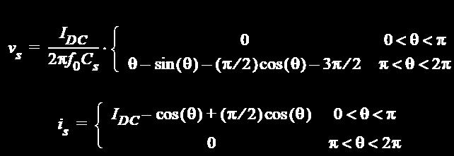
40 General Class E/F Design A switch with parallel capacitance, an ideal choke, and a possibly countable infinite number of harmonic impedances.


41 Switch/Cap Current The switch carries an impulsive current component due to cap discharge.


42 Cap Voltage The voltage across the capacitor is calculated from the current. The harmonic impedance constraint implies the following relations.


43 Constraint Equations There are T complex valued equations and one real valued equation and T +2 unknowns. These equations can be solved for Q and i x The ZVS solution has an additional constraint Q=0.

44 ZVS It can be shown that ZVS implies that: (R 1,X 1 ) is the fundamental load impedance. The center and radius of the circle is determined by the overtone network.

45 ZdVS The ZdVS conditions generate additional constraints.

46 Class E/F Amplifier Family Are there other interesting tuning networks besides the well known Class E and F?
47 Switching Amplifier Wish List ZVS Switching Inclusion of device output capacitance Simple circuit implementation Lower peak voltage (F v ) Lower RMS current (F i ) Capacitance Tolerance (F c )


48 Class E versus F Consider a hybrid of Class E and F with desirable properties of both. Construct such a hybrid by choosing harmonics to either satisfy Class E or F conditions. Note that the fundamental load is set by Class E ZVS conditions.


49 Class E/F Family

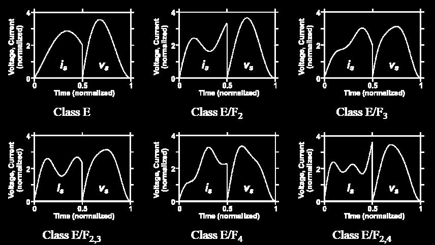
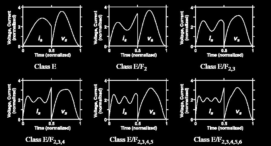
50 Example Class E/F Waveforms

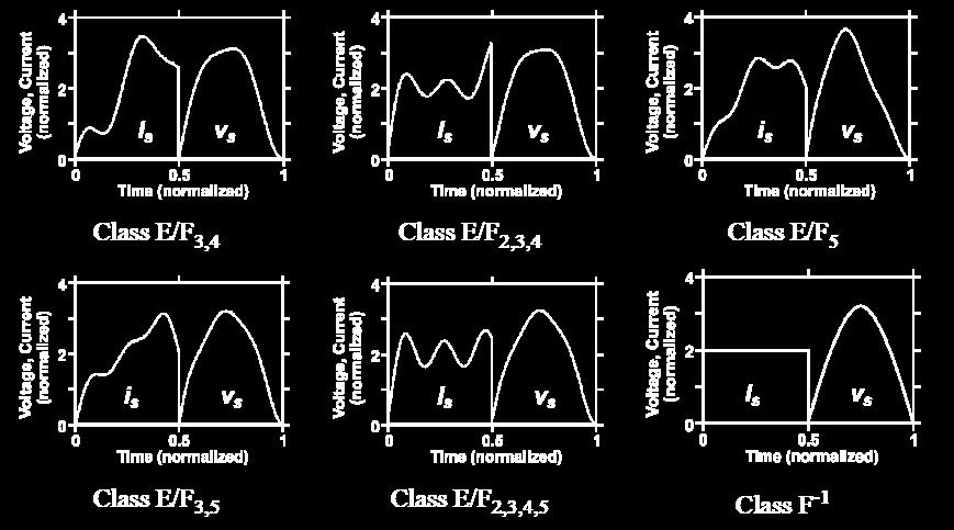
51 More Waveforms

52 Single Harmonic Class E/F

53 Odd Harmonic Class E/F

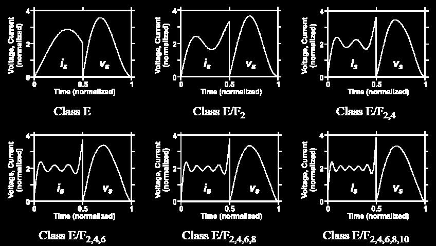
54 Even Harmonic Class E/F
55 N-Harmonic Class E/F
56 Overall Comparison
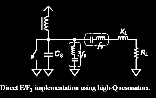
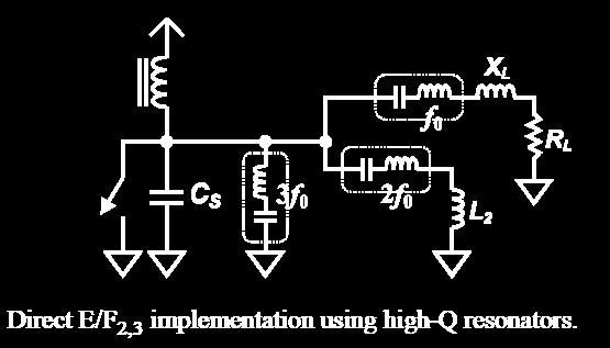
57 Direct Implementation

58 Push-Pull Amplifiers Creation of virtual grounds at odd harmonics and open circuits at even harmonics is very handy for designing class E/F amplifiers.

59 Class E/F 3 Push-Pull Short at third harmonic. Does not need to be high Q since even harmonics don t see it
60 Even & Odd Harmonic Control Odd harmonics only see Z D /2 since Y C is shorted to ground. Even harmonics see Y c to ground

61 Switching Amplifier Landscape
62 Class E/F odd Amplifier All odd harmonics see small impedance (ideally short) whereas even harmonics do not see shunt LC tank.
TUNED AMPLIFIERS 5.1 Introduction: Coil Losses:
 TUNED AMPLIFIERS 5.1 Introduction: To amplify the selective range of frequencies, the resistive load R C is replaced by a tuned circuit. The tuned circuit is capable of amplifying a signal over a narrow
Lecture 20: Passive Mixers
 EECS 142 Lecture 20: Passive Mixers Prof. Ali M. Niknejad University of California, Berkeley Copyright c 2005 by Ali M. Niknejad A. M. Niknejad University of California, Berkeley EECS 142 Lecture 20 p.
A New Topology of Load Network for Class F RF Power Amplifiers
 A New Topology of Load Network for Class F RF Firas Mohammed Ali Al-Raie Electrical Engineering Department, University of Technology/Baghdad. Email: 30204@uotechnology.edu.iq Received on:12/1/2016 & Accepted
Berkeley. The ABC s of PA s. Prof. Ali M. Niknejad. U.C. Berkeley Copyright c 2014 by Ali M. Niknejad
 Berkeley The ABC s of PA s Prof. Ali M. U.C. Berkeley Copyright c 2014 by Ali M. Class A Review Class A Amplifiers Class A amplifiers have a collector current waveform with 100% duty cycle. In other words,
Radio Frequency Electronics
 Radio Frequency Electronics Tuned Amplifiers John Battiscombe Gunn Born in 1928 in Egypt (father was a famous Egyptologist), and was Educated in England Worked at IBM s Thomas J. Watson Research Center
Expansion of class-j power amplifiers into inverse mode operation
 Expansion of class-j power amplifiers into inverse mode operation Youngcheol Par a) Dept. of Electronics Eng., Hanu University of Foreign Studies Yongin-si, Kyunggi-do 449 791, Republic of Korea a) ycpar@hufs.ac.r
Introduction to CMOS RF Integrated Circuits Design
 VII. ower Amplifiers VII-1 Outline Functionality Figures of Merit A Design Classical Design (Class A, B, C) High-Efficiency Design (Class E, F) Matching Network Linearity T/R Switches VII-2 As and TRs
ANALYSIS OF BROADBAND GAN SWITCH MODE CLASS-E POWER AMPLIFIER
 Progress In Electromagnetics Research Letters, Vol. 38, 151 16, 213 ANALYSIS OF BROADBAND GAN SWITCH MODE CLASS-E POWER AMPLIFIER Ahmed Tanany, Ahmed Sayed *, and Georg Boeck Berlin Institute of Technology,
Transmission Lines. Ranga Rodrigo. January 13, Antennas and Propagation: Transmission Lines 1/46
 Transmission Lines Ranga Rodrigo January 13, 2009 Antennas and Propagation: Transmission Lines 1/46 1 Basic Transmission Line Properties 2 Standing Waves Antennas and Propagation: Transmission Lines Outline
1 GHz Current Mode Class-D Power Amplifier in Hybrid Technology Using GaN HEMTs
 ROMANIAN JOURNAL OF INFORMATION SCIENCE AND TECHNOLOGY Volume 11, Number 4, 2008, 319 328 1 GHz Current Mode Class-D Power Amplifier in Hybrid Technology Using GaN HEMTs Pouya AFLAKI, Renato NEGRA, Fadhel
Two-output Class E Isolated dc-dc Converter at 5 MHz Switching Frequency 1 Z. Pavlović, J.A. Oliver, P. Alou, O. Garcia, R.Prieto, J.A.
 Two-output Class E Isolated dc-dc Converter at 5 MHz Switching Frequency 1 Z. Pavlović, J.A. Oliver, P. Alou, O. Garcia, R.Prieto, J.A. Cobos Universidad Politécnica de Madrid Centro de Electrónica Industrial
UNIVERSITY OF BABYLON BASIC OF ELECTRICAL ENGINEERING LECTURE NOTES. Resonance
 Resonance The resonant(or tuned) circuit, in one of its many forms, allows us to select a desired radio or television signal from the vast number of signals that are around us at any time. Resonant electronic
EECS 117. Lecture 5: Transmission Line Impedance Matching. Prof. Niknejad. University of California, Berkeley
 EECS 117 Lecture 5: Transmission Line Impedance Matching Prof. Niknejad University of California, Berkeley University of California, Berkeley EECS 117 Lecture 5 p. 1/2 Open Line I/V The open transmission
Design of Class-E M Power Amplifier Taking into Account Auxiliary Circuit
 Design of Class-E M Power Amplifier Taking into Account Auxiliary Circuit Ryosuke MIYAHARA,HirooSEKIYA, and Marian K. KAZIMIERCZUK Dept. of Information and Image Science, Chiba University -33, Yayoi-cho,
Design of Class F Power Amplifiers Using Cree GaN HEMTs and Microwave Office Software to Optimize Gain, Efficiency, and Stability
 White Paper Design of Class F Power Amplifiers Using Cree GaN HEMTs and Microwave Office Software to Optimize Gain, Efficiency, and Stability Overview This white paper explores the design of power amplifiers
Chapter 11. Alternating Current
 Unit-2 ECE131 BEEE Chapter 11 Alternating Current Objectives After completing this chapter, you will be able to: Describe how an AC voltage is produced with an AC generator (alternator) Define alternation,
SIDDHARTH GROUP OF INSTITUTIONS :: PUTTUR (AUTONOMOUS) Siddharth Nagar, Narayanavanam Road QUESTION BANK
 Siddharth Nagar, Narayanavanam Road QUESTION BANK") SIDDHARTH GROUP OF INSTITUTIONS :: PUTTUR (AUTONOMOUS) Siddharth Nagar, Narayanavanam Road 517583 QUESTION BANK Subject with Code : Electronic Circuit Analysis (16EC407) Year & Sem: II-B.Tech & II-Sem
SIDDHARTH GROUP OF INSTITUTIONS :: PUTTUR (AUTONOMOUS) Siddharth Nagar, Narayanavanam Road 517583 QUESTION BANK Subject with Code : Electronic Circuit Analysis (16EC407) Year & Sem: II-B.Tech & II-Sem
Chapter 2. The Fundamentals of Electronics: A Review
 Chapter 2 The Fundamentals of Electronics: A Review Topics Covered 2-1: Gain, Attenuation, and Decibels 2-2: Tuned Circuits 2-3: Filters 2-4: Fourier Theory 2-1: Gain, Attenuation, and Decibels Most circuits
EE301 ELECTRONIC CIRCUITS CHAPTER 2 : OSCILLATORS. Lecturer : Engr. Muhammad Muizz Bin Mohd Nawawi
 EE301 ELECTRONIC CIRCUITS CHAPTER 2 : OSCILLATORS Lecturer : Engr. Muhammad Muizz Bin Mohd Nawawi 2.1 INTRODUCTION An electronic circuit which is designed to generate a periodic waveform continuously at
Design of a Current-Mode Class-D Power Amplifier in RF-CMOS
 Design of a Current-Mode Class-D Power Amplifier in RF-CMOS Daniel Oliveira, Cândido Duarte, Vítor Grade Tavares, and Pedro Guedes de Oliveira Microelectronics Students Group, Department of Electrical
Chapter.8: Oscillators
 Chapter.8: Oscillators Objectives: To understand The basic operation of an Oscillator the working of low frequency oscillators RC phase shift oscillator Wien bridge Oscillator the working of tuned oscillator
The steeper the phase shift as a function of frequency φ(ω) the more stable the frequency of oscillation
 the more stable the frequency of oscillation") It should be noted that the frequency of oscillation ω o is determined by the phase characteristics of the feedback loop. the loop oscillates at the frequency for which the phase is zero The steeper the
It should be noted that the frequency of oscillation ω o is determined by the phase characteristics of the feedback loop. the loop oscillates at the frequency for which the phase is zero The steeper the
Class XII Chapter 7 Alternating Current Physics
 Question 7.1: A 100 Ω resistor is connected to a 220 V, 50 Hz ac supply. (a) What is the rms value of current in the circuit? (b) What is the net power consumed over a full cycle? Resistance of the resistor,
Chapter 13 Oscillators and Data Converters
 Chapter 13 Oscillators and Data Converters 13.1 General Considerations 13.2 Ring Oscillators 13.3 LC Oscillators 13.4 Phase Shift Oscillator 13.5 Wien-Bridge Oscillator 13.6 Crystal Oscillators 13.7 Chapter
Communication Circuit Lab Manual
 German Jordanian University School of Electrical Engineering and IT Department of Electrical and Communication Engineering Communication Circuit Lab Manual Experiment 2 Tuned Amplifier Eng. Anas Alashqar
ISSCC 2002 / SESSION 17 / ADVANCED RF TECHNIQUES / 17.2
 ISSCC 2002 / SESSION 17 / ADVANCED RF TECHNIQUES / 17.2 17.2 A CMOS Differential Noise-Shifting Colpitts VCO Roberto Aparicio, Ali Hajimiri California Institute of Technology, Pasadena, CA Demand for higher
CHOICE OF HIGH FREQUENCY INVERTERS AND SEMICONDUCTOR SWITCHES
 Chapter-3 CHOICE OF HIGH FREQUENCY INVERTERS AND SEMICONDUCTOR SWITCHES This chapter is based on the published articles, 1. Nitai Pal, Pradip Kumar Sadhu, Dola Sinha and Atanu Bandyopadhyay, Selection
High Efficiency Classes of RF Amplifiers
 Rok / Year: Svazek / Volume: Číslo / Number: Jazyk / Language 2018 20 1 EN High Efficiency Classes of RF Amplifiers - Erik Herceg, Tomáš Urbanec urbanec@feec.vutbr.cz, herceg@feec.vutbr.cz Faculty of Electrical
TUNED AMPLIFIERS. Tank circuits.
 Tank circuits. TUNED AMPLIFIERS Analysis of single tuned amplifier, Double tuned, stagger tuned amplifiers. Instability of tuned amplifiers, stabilization techniques, Narrow band neutralization using coil,
Feedback and Oscillator Circuits
 Chapter 14 Chapter 14 Feedback and Oscillator Circuits Feedback Concepts The effects of negative feedback on an amplifier: Disadvantage Lower gain Advantages Higher input impedance More stable gain Improved
Design of Resistive-Input Class E Resonant Rectifiers for Variable-Power Operation
 14th IEEE Workshop on Control and Modeling for Power Electronics COMPEL '13), June 2013. Design of Resistive-Input Class E Resonant Rectifiers for Variable-Power Operation Juan A. Santiago-González, Khurram
MAHALAKSHMI ENGINEERING COLLEGE TIRUCHIRAPALLI UNIT III TUNED AMPLIFIERS PART A (2 Marks)
") MAHALAKSHMI ENGINEERING COLLEGE TIRUCHIRAPALLI-621213. UNIT III TUNED AMPLIFIERS PART A (2 Marks) 1. What is meant by tuned amplifiers? Tuned amplifiers are amplifiers that are designed to reject a certain
MAHALAKSHMI ENGINEERING COLLEGE TIRUCHIRAPALLI-621213. UNIT III TUNED AMPLIFIERS PART A (2 Marks) 1. What is meant by tuned amplifiers? Tuned amplifiers are amplifiers that are designed to reject a certain
Oscillators. An oscillator may be described as a source of alternating voltage. It is different than amplifier.
 Oscillators An oscillator may be described as a source of alternating voltage. It is different than amplifier. An amplifier delivers an output signal whose waveform corresponds to the input signal but
HIGH-EFFICIENCY RF AND MICROWAVE POWER AMPLIFIERS: HISTORICAL ASPECT AND MODERN TRENDS. Dr. Andrei Grebennikov
 9 adio and Wireless Week Power Amplifier Symposium HIGH-EFFIIENY F AND MIOWAVE POWE AMPIFIES: HISTOIA ASPET AND MODEN TENDS Dr. Andrei Grebennikov grandrei@ieee.org HIGH-EFFIIENY F AND MIOWAVE POWE AMPIFIES:
Linear electronic. Lecture No. 1
 1 Lecture No. 1 2 3 4 5 Lecture No. 2 6 7 8 9 10 11 Lecture No. 3 12 13 14 Lecture No. 4 Example: find Frequency response analysis for the circuit shown in figure below. Where R S =4kR B1 =8kR B2 =4k R
Figure 1: Closed Loop System
 SIGNAL GENERATORS 3. Introduction Signal sources have a variety of applications including checking stage gain, frequency response, and alignment in receivers and in a wide range of other electronics equipment.
Tuned Circuits With Inductive Feedback - A Time Domain Approach
 Tuned Circuits With Inductive Feedback - A Time Domain Approach Dipl.-Phys. Jochen Bauer 02/05/2013 Abstract In this paper, lossy tuned circuits with feedback provided inductively by a so-called tickler
A 1-W GaAs Class-E Power Amplifier with an FBAR Filter Embedded in the Output Network
 A 1-W GaAs Class-E Power Amplifier with an FBAR Filter Embedded in the Output Network Kyle Holzer and Jeffrey S. Walling University of Utah PERFIC Lab, Salt Lake City, UT 84112, USA Abstract Integration
FGJTCFWP"KPUVKVWVG"QH"VGEJPQNQI[" FGRCTVOGPV"QH"GNGEVTKECN"GPIKPGGTKPI" VGG"246"JKIJ"XQNVCIG"GPIKPGGTKPI
 FGJTFWP"KPUKWG"QH"GEJPQNQI[" FGRTOGP"QH"GNGETKEN"GPIKPGGTKPI" GG"46"JKIJ"XQNIG"GPIKPGGTKPI Resonant Transformers: The fig. (b) shows the equivalent circuit of a high voltage testing transformer (shown
CHAPTER 3 DC-DC CONVERTER TOPOLOGIES
 47 CHAPTER 3 DC-DC CONVERTER TOPOLOGIES 3.1 INTRODUCTION In recent decades, much research efforts are directed towards finding an isolated DC-DC converter with high volumetric power density, low electro
Transmission Lines. Ranga Rodrigo. January 27, Antennas and Propagation: Transmission Lines 1/72
 Transmission Lines Ranga Rodrigo January 27, 2009 Antennas and Propagation: Transmission Lines 1/72 1 Standing Waves 2 Smith Chart 3 Impedance Matching Series Reactive Matching Shunt Reactive Matching
Conventional Paper-II-2013
 1. All parts carry equal marks Conventional Paper-II-013 (a) (d) A 0V DC shunt motor takes 0A at full load running at 500 rpm. The armature resistance is 0.4Ω and shunt field resistance of 176Ω. The machine
UNIT 1 MULTI STAGE AMPLIFIES
 UNIT 1 MULTI STAGE AMPLIFIES 1. a) Derive the equation for the overall voltage gain of a multistage amplifier in terms of the individual voltage gains. b) what are the multi-stage amplifiers? 2. Describe
 Code No: Y0221/R07 Set No. 1 I B.Tech Supplementary Examinations, Apr/May 2013 BASIC ELECTRONIC DEVICES AND CIRCUITS (Electrical & Electronics Engineering) Time: 3 hours Max Marks: 80 Answer any FIVE Questions
OSCILLATORS AND WAVEFORM-SHAPING CIRCUITS
 OSILLATORS AND WAVEFORM-SHAPING IRUITS Signals having prescribed standard waveforms (e.g., sinusoidal, square, triangle, pulse, etc). To generate sinusoidal waveforms: o Positive feedback loop with non-linear
8322 IEEE TRANSACTIONS ON POWER ELECTRONICS, VOL. 32, NO. 11, NOVEMBER Class-E Half-Wave Zero dv/dt Rectifiers for Inductive Power Transfer
 8322 IEEE TRANSACTIONS ON POWER ELECTRONICS, VOL. 32, NO. 11, NOVEMBER 2017 Class-E Half-Wave Zero dv/dt Rectifiers for Inductive Power Transfer George Kkelis, Student Member, IEEE, David C. Yates, Member,
Code: 9A Answer any FIVE questions All questions carry equal marks *****
 II B. Tech II Semester (R09) Regular & Supplementary Examinations, April/May 2012 ELECTRONIC CIRCUIT ANALYSIS (Common to EIE, E. Con. E & ECE) Time: 3 hours Max Marks: 70 Answer any FIVE questions All
EMERGING technologies such as wireless power transfer
 IEEE TRANSACTIONS ON POWER ELECTRONICS, VOL. 3, NO. 5, MAY 06 345 Modeling and Analysis of Class EF and Class E/F Inverters With Series-Tuned Resonant Networks Samer Aldhaher, David C. Yates, Member, IEEE,
A.C. Circuits -- Conceptual Solutions
 A.C. Circuits -- Conceptual Solutions 1.) Charge carriers in a DC circuit move in one direction only. What do charge carriers do in an AC circuit? Solution: The voltage difference between the terminals
UNIT _ III MCQ. Ans : C. Ans : C. Ans : C
 UNIT _ III MCQ Ans : C Ans : C Ans : C Ans : A Ans : B Multiple Choice Questions and Answers on Transistor Tuned Amplifiers Q1. A tuned amplifier uses. load 1. Resistive 2. Capacitive 3. LC tank 4. Inductive
University of Twente
 University of Twente Faculty of Electrical Engineering, Mathematics & Computer Science The design of a new power combining technique for the RF power amplifiers Wei Cheng MSc. Thesis May 6 Supervisors:
Lecture 17: BJT/FET Mixers/Mixer Noise
 EECS 142 Lecture 17: BJT/FET Mixers/Mixer Noise Prof. Ali M. Niknejad University of California, Berkeley Copyright c 2005 by Ali M. Niknejad A. M. Niknejad University of California, Berkeley EECS 142 Lecture
EC Transmission Lines And Waveguides
 EC6503 - Transmission Lines And Waveguides UNIT I - TRANSMISSION LINE THEORY A line of cascaded T sections & Transmission lines - General Solution, Physical Significance of the Equations 1. Define Characteristic
RC circuit. Recall the series RC circuit.
 RC circuit Recall the series RC circuit. If C is discharged and then a constant voltage V is suddenly applied, the charge on, and voltage across, C is initially zero. The charge ultimately reaches the
OPERATIONAL AMPLIFIER PREPARED BY, PROF. CHIRAG H. RAVAL ASSISTANT PROFESSOR NIRMA UNIVRSITY
 OPERATIONAL AMPLIFIER PREPARED BY, PROF. CHIRAG H. RAVAL ASSISTANT PROFESSOR NIRMA UNIVRSITY INTRODUCTION Op-Amp means Operational Amplifier. Operational stands for mathematical operation like addition,
Electronic Circuits. Power Amplifiers. Manar Mohaisen Office: F208 Department of EECE
 Electronic Circuits Power Amplifiers Manar Mohaisen Office: F208 Email: manar.subhi@kut.ac.kr Department of EECE Review of the Precedent Lecture Explain the Amplifier Operation Explain the BJT AC Models
EVALUATION KIT AVAILABLE 10MHz to 1050MHz Integrated RF Oscillator with Buffered Outputs. Typical Operating Circuit. 10nH 1000pF MAX2620 BIAS SUPPLY
 19-1248; Rev 1; 5/98 EVALUATION KIT AVAILABLE 10MHz to 1050MHz Integrated General Description The combines a low-noise oscillator with two output buffers in a low-cost, plastic surface-mount, ultra-small
Chapter 6: Power Amplifiers
 Chapter 6: Power Amplifiers Contents Class A Class B Class C Power Amplifiers Class A, B and C amplifiers are used in transmitters Tuned with a band width wide enough to pass all information sidebands
Design of a Regenerative Receiver for the Short-Wave Bands A Tutorial and Design Guide for Experimental Work. Part I
 Design of a Regenerative Receiver for the Short-Wave Bands A Tutorial and Design Guide for Experimental Work Part I Ramón Vargas Patrón rvargas@inictel-uni.edu.pe INICTEL-UNI Regenerative Receivers remain
Small signal Amplifier stages. Figure 5.2 Classification of power amplifiers
 5.1 Introduction When the power requirement to drive the load is in terms of several Watts rather than mili-watts the power amplifiers are used. Power amplifiers form the last stage of multistage amplifiers.
Lecture (10) Power Amplifiers (2)
 Power Amplifiers (2)") Lecture (10) Power Amplifiers (2) By: Dr. Ahmed ElShafee ١ Class B/AB Power the ideal maximum peak output current for both dual supply and single supply push pull amplifiers is approximately Ic(sat), and
Lecture (10) Power Amplifiers (2) By: Dr. Ahmed ElShafee ١ Class B/AB Power the ideal maximum peak output current for both dual supply and single supply push pull amplifiers is approximately Ic(sat), and
High Frequency Amplifiers
 EECS 142 Laboratory #3 High Frequency Amplifiers A. M. Niknejad Berkeley Wireless Research Center University of California, Berkeley 2108 Allston Way, Suite 200 Berkeley, CA 94704-1302 October 27, 2008
Communication Circuit Lab Manual
 German Jordanian University School of Electrical Engineering and IT Department of Electrical and Communication Engineering Communication Circuit Lab Manual Experiment 3 Crystal Oscillator Eng. Anas Alashqar
6.976 High Speed Communication Circuits and Systems Lecture 8 Noise Figure, Impact of Amplifier Nonlinearities
 6.976 High Speed Communication Circuits and Systems Lecture 8 Noise Figure, Impact of Amplifier Nonlinearities Michael Perrott Massachusetts Institute of Technology Copyright 2003 by Michael H. Perrott
EE 42/100 Lecture 16: Inductance. Rev B 3/15/2010 (8:55 PM) Prof. Ali M. Niknejad
 Prof. Ali M. Niknejad") A. M. Niknejad University of California, Berkeley EE 100 / 42 Lecture 16 p. 1/23 EE 42/100 Lecture 16: Inductance ELECTRONICS Rev B 3/15/2010 (8:55 PM) Prof. Ali M. Niknejad University of California, Berkeley
A. M. Niknejad University of California, Berkeley EE 100 / 42 Lecture 16 p. 1/23 EE 42/100 Lecture 16: Inductance ELECTRONICS Rev B 3/15/2010 (8:55 PM) Prof. Ali M. Niknejad University of California, Berkeley
Code No: R Set No. 1
 Code No: R059210404 Set No. 1 II B.Tech I Semester Supplimentary Examinations, February 2008 ELECTRONIC CIRCUIT ANALYSIS ( Common to Electronics & Communication Engineering and Electronics & Telematics)
CHAPTER 4 MEASUREMENT OF NOISE SOURCE IMPEDANCE
 69 CHAPTER 4 MEASUREMENT OF NOISE SOURCE IMPEDANCE 4.1 INTRODUCTION EMI filter performance depends on the noise source impedance of the circuit and the noise load impedance at the test site. The noise
Push-Pull Class-E Power Amplifier with a Simple Load Network Using an Impedance Matched Transformer
 Proceedings of the International Conference on Electrical, Electronics, Computer Engineering and their Applications, Kuala Lumpur, Malaysia, 214 Push-Pull Class-E Power Amplifier with a Simple Load Network
Introduction... 1 Part I: Getting Started with Circuit Analysis Part II: Applying Analytical Methods for Complex Circuits...
 Contents at a Glance Introduction... 1 Part I: Getting Started with Circuit Analysis... 5 Chapter 1: Introducing Circuit Analysis...7 Chapter 2: Clarifying Basic Circuit Concepts and Diagrams...15 Chapter
Downloaded from edlib.asdf.res.in
 ASDF India Proceedings of the Intl. Conf. on Innovative trends in Electronics Communication and Applications 2014 242 Design and Implementation of Ultrasonic Transducers Using HV Class-F Power Amplifier
Modeling and Simulation of Paralleled Series-Loaded-Resonant Converter
 Second Asia International Conference on Modelling & Simulation Modeling and Simulation of Paralleled Series-Loaded-Resonant Converter Alejandro Polleri (1), Taufik (1), and Makbul Anwari () (1) Electrical
Conventional Single-Switch Forward Converter Design
 Maxim > Design Support > Technical Documents > Application Notes > Amplifier and Comparator Circuits > APP 3983 Maxim > Design Support > Technical Documents > Application Notes > Power-Supply Circuits
Electronics 1. Voltage/Current Resistors Capacitors Inductors Transistors
 Electronics 1 Voltage/Current Resistors Capacitors Inductors Transistors Voltage and Current Simple circuit a battery pushes some electrons around the circuit how many per second? Water The easiest way
Paper-1 (Circuit Analysis) UNIT-I
 UNIT-I") Paper-1 (Circuit Analysis) UNIT-I AC Fundamentals & Kirchhoff s Current and Voltage Laws 1. Explain how a sinusoidal signal can be generated and give the significance of each term in the equation? 2. Define
Paper-1 (Circuit Analysis) UNIT-I AC Fundamentals & Kirchhoff s Current and Voltage Laws 1. Explain how a sinusoidal signal can be generated and give the significance of each term in the equation? 2. Define
Low Pass Filter Introduction
 Low Pass Filter Introduction Basically, an electrical filter is a circuit that can be designed to modify, reshape or reject all unwanted frequencies of an electrical signal and accept or pass only those
AC Circuits INTRODUCTION DISCUSSION OF PRINCIPLES. Resistance in an AC Circuit
 AC Circuits INTRODUCTION The study of alternating current 1 (AC) in physics is very important as it has practical applications in our daily lives. As the name implies, the current and voltage change directions
Chapter 6 Soft-Switching dc-dc Converters Outlines
 Chapter 6 Soft-Switching dc-dc Converters Outlines Classification of soft-switching resonant converters Advantages and disadvantages of ZCS and ZVS Zero-current switching topologies The resonant switch
WEAKLY coupled inductive links, Fig. 1, tend to operate. Class-E Half-Wave Zero dv/dt Rectifiers for Inductive Power Transfer
 1 Class-E Half-Wave Zero dv/dt Rectifiers for Inductive Power Transfer George Kkelis, Student Member, IEEE, David C. Yates, Member, IEEE, and Paul D. Mitcheson, Senior Member, IEEE. Abstract This paper
The efficiency of a FET is degraded
 REVIEW BOARD MWJ APPROVED A Field-Effect Transistor That Avoids Pinch-Off Alfred Grayzel Planar Monolithic Industries Inc., Frederick, Md. Greater efficiency and output power are proposed by providing
RF Power Amplifier (RFPA) Designing a 'Output Tank Circuit'
 Designing a 'Output Tank Circuit'") RF Power Amplifier (RFPA) Designing a 'Output Tank Circuit' By Larry E. Gugle K4RFE, RF Design, Manufacture, Test & Service Engineer (Retired) Figure-1 Output 'Tank' Circuit Network in Low-Pass Filter
RF Power Amplifier (RFPA) Designing a 'Output Tank Circuit' By Larry E. Gugle K4RFE, RF Design, Manufacture, Test & Service Engineer (Retired) Figure-1 Output 'Tank' Circuit Network in Low-Pass Filter
Case Study: Osc2 Design of a C-Band VCO
 MICROWAVE AND RF DESIGN Case Study: Osc2 Design of a C-Band VCO Presented by Michael Steer Reading: Chapter 20, 20.5,6 Index: CS_Osc2 Based on material in Microwave and RF Design: A Systems Approach, 2
UNIT 1 CIRCUIT ANALYSIS 1 What is a graph of a network? When all the elements in a network is replaced by lines with circles or dots at both ends.
 UNIT 1 CIRCUIT ANALYSIS 1 What is a graph of a network? When all the elements in a network is replaced by lines with circles or dots at both ends. 2 What is tree of a network? It is an interconnected open
Voltage and Current Waveforms Enhancement using Harmonic Filters
 Voltage and Current Waveforms Enhancement using Harmonic Filters Rajeb Ibsaim rabsaim@yahoo.com, Azzawia University, Libya Amer Daeri ibnjubair1@yahoo.co.uk Azzawia University, Libya Abstract The demand
An active filter offers the following advantages over a passive filter:
 ACTIVE FILTERS An electric filter is often a frequency-selective circuit that passes a specified band of frequencies and blocks or attenuates signals of frequencies outside this band. Filters may be classified
SETH JAI PARKASH POLYTECHNIC, DAMLA
 SETH JAI PARKASH POLYTECHNIC, DAMLA NAME OF FACULTY----------SANDEEP SHARMA DISCIPLINE---------------------- E.C.E (S.F) SEMESTER-------------------------2 ND SUBJECT----------------------------BASIC ELECTRONICS
Owner. Dale Nelson. Design Team. Chief Scientist. Business Manager. Dale Nelson. Dale Nelson Dale Nelson. Dale Nelson. Dale Nelson
 DHN Integrated Circuit Design Designing Crystal Oscillators Dale Nelson, Ph.D. DHN Integrated Circuit Design Established in Sept. 2005 Design Expertise: Crystal Oscillators Phase Locked Loops General Analog/Mixed
Design and simulation of Parallel circuit class E Power amplifier
 International Journal of scientific research and management (IJSRM) Volume 3 Issue 7 Pages 3270-3274 2015 \ Website: www.ijsrm.in ISSN (e): 2321-3418 Design and simulation of Parallel circuit class E Power
6.776 High Speed Communication Circuits and Systems Lecture 14 Voltage Controlled Oscillators
 6.776 High Speed Communication Circuits and Systems Lecture 14 Voltage Controlled Oscillators Massachusetts Institute of Technology March 29, 2005 Copyright 2005 by Michael H. Perrott VCO Design for Narrowband
Subject Code: Model Answer Page No: / N
 Important Instructions to examiners: 1) The answers should be examined by key words and not as word-to-word as given in the model answer scheme. 2) The model answer and the answer written by candidate
Outline. Noise and Distortion. Noise basics Component and system noise Distortion INF4420. Jørgen Andreas Michaelsen Spring / 45 2 / 45
 INF440 Noise and Distortion Jørgen Andreas Michaelsen Spring 013 1 / 45 Outline Noise basics Component and system noise Distortion Spring 013 Noise and distortion / 45 Introduction We have already considered
Understanding VCO Concepts
 Understanding VCO Concepts OSCILLATOR FUNDAMENTALS An oscillator circuit can be modeled as shown in Figure 1 as the combination of an amplifier with gain A (jω) and a feedback network β (jω), having frequency-dependent
Designers Series XII. Switching Power Magazine. Copyright 2005
 Designers Series XII n this issue, and previous issues of SPM, we cover the latest technologies in exotic high-density power. Most power supplies in the commercial world, however, are built with the bread-and-butter
Simplified Analysis and Design of Seriesresonant LLC Half-bridge Converters
 Simplified Analysis and Design of Seriesresonant LLC Half-bridge Converters MLD GROUP INDUSTRIAL & POWER CONVERSION DIVISION Off-line SMPS BU Application Lab Presentation Outline LLC series-resonant Half-bridge:
UNIT 2. Q.1) Describe the functioning of standard signal generator. Ans. Electronic Measurements & Instrumentation
 Describe the functioning of standard signal generator. Ans. Electronic Measurements & Instrumentation") UNIT 2 Q.1) Describe the functioning of standard signal generator Ans. STANDARD SIGNAL GENERATOR A standard signal generator produces known and controllable voltages. It is used as power source for the
UNIT 2 Q.1) Describe the functioning of standard signal generator Ans. STANDARD SIGNAL GENERATOR A standard signal generator produces known and controllable voltages. It is used as power source for the
Section 4: Operational Amplifiers
 Section 4: Operational Amplifiers Op Amps Integrated circuits Simpler to understand than transistors Get back to linear systems, but now with gain Come in various forms Comparators Full Op Amps Differential
Homework Assignment 05
 Homework Assignment 05 Question (2 points each unless otherwise indicated)(20 points). Estimate the parallel parasitic capacitance of a mh inductor with an SRF of 220 khz. Answer: (2π)(220 0 3 ) = ( 0
Exact Time-Domain Analysis of Class E Power Amplifiers with Quarterwave Transmission Line
 Exact Time-Domain Analysis of lass E Power Amplifiers with Quarterwave Transmission ine Andrei Grebennikov, Member, IEEE Abstract The results of exact time domain analysis of the switched-mode tuned lass
CHAPTER 2 A SERIES PARALLEL RESONANT CONVERTER WITH OPEN LOOP CONTROL
 14 CHAPTER 2 A SERIES PARALLEL RESONANT CONVERTER WITH OPEN LOOP CONTROL 2.1 INTRODUCTION Power electronics devices have many advantages over the traditional power devices in many aspects such as converting
Study of Inductive and Capacitive Reactance and RLC Resonance
 Objective Study of Inductive and Capacitive Reactance and RLC Resonance To understand how the reactance of inductors and capacitors change with frequency, and how the two can cancel each other to leave
PART MAX2605EUT-T MAX2606EUT-T MAX2607EUT-T MAX2608EUT-T MAX2609EUT-T TOP VIEW IND GND. Maxim Integrated Products 1
 19-1673; Rev 0a; 4/02 EVALUATION KIT MANUAL AVAILABLE 45MHz to 650MHz, Integrated IF General Description The are compact, high-performance intermediate-frequency (IF) voltage-controlled oscillators (VCOs)