CSE 370 Winter Homework 5 Solutions
|
|
|
- Nathaniel Townsend
- 5 years ago
- Views:
Transcription
 a) add1 b)")
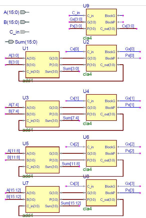
1 CSE 370 Winter 2008 Homework 5 Solutions 1) Carry Look-Ahead Adder (CLA) a) add1 b) add4
2 c) cla4
3 d) cla16
4 e) Gate Count: 118 gates add1 : 3 gates add4 : 4*Add1 = 12 gates cla4 : 14 gates cla16: (4*Add4) + (5*Cla4) = = 118 gates Delay: Look at the schematic for add16 above. The A and B inputs first go through add4 blocks. In the add4, they produce the P and G signals. This takes 1 gate delay. They also produce a sum; however the carry input to the gate producing the sum hasn t arrived yet. So we do not consider the sum now. The P and G signals produced by any add4 block, say U1, goes into a cla4 U2. In the cla4, it takes 2 gate delays to produce a blockp and a blockg. The cla4 also produces carry output bits, however the carry in required to compute the cout hasn t arrived yet. So we do not consider the cout now. The blockp s and blockg s from the cla4 s U2, U4, U6 and U8 are available at the same time. These are fed to the cla4 - U9. In U9, the Carry in is available and hence it computes the cout bits. In the worst case, it takes 2 gate delays to do this. The blockp and blockg output of U9 is available at this time (5 gate delays for BlockP and G signals). The carry bits produced by U9 are fed back into cla4 s U2, U4, U6 and U8. Only now are the carry in bits available to these four blocks. Hence now we consider the cout of these blocks. It takes 2 gate delays to produce the cout bits in the worst case. These cout bits act as the carry in bits for the add4 blocks U1, U3, U5 and U7. Only now have its carry in bits arrived. So now we can consider the sum. From the time the carry in bit arrives it takes only 1 gate delay to compute the sum output. The other input to the XOR gate was computed long before and hence we do not worry about the gate it traverses through. Total: = 8 gate delays. f) Yes. A cla64 would simply have 4 cla16 s and use 1 cla4 that takes the blockg and blockp signals from the cla16 s to generate the carry inputs for each of the cla16 s. Gate Count: (4*cla16) + cla4 = 486 Delay: 5 gate delays for blockp and blockg of cla16 (see above). 2 gate delays in the cla4 to produce the carry in for the cla16 s. Once the cla16 has its carry input it takes only 5 gate delays to produce the sum as its bit-wise P &G has already been computed. Total: =12

![Then the CSA_1 st component makes the following (very straightforward) connections to the 16 FAs: A[i] A i B[i] B i Sum[i]](/docs-images/95/126092227/images/5-1.jpg "Sum i Carry[i] C out i The following answers make use of a component [<<] which denotes a left shift by one bit.")
5 2) a) The first stage of the carry save adder (CSA_1 st ) consists of 16 full adders (FA). Call the inputs of the i th FA A i, B i, C in i and the outputs Sum i and C out i. Then the CSA_1 st component makes the following (very straightforward) connections to the 16 FAs: A[i] A i B[i] B i Sum[i] Sum i Carry[i] C out i The following answers make use of a component [<<] which denotes a left shift by one bit. Normally one would accomplish this by setting O[15:1] = I[14:0], O[0] = GND. b)

6 c)
7 3) a) makepg: add1 block with just P and G outputs. Or you can reuse add1 just leaving Sum output unconnected. b) make4pg: same concept as above, applied to add4. c) S = P XOR C in ; Co = G + PC in d) 16 bit adder: This architecture is called a carry skip or a carry bypass adder. Simply chain together 4 of the ones in the question e) Why this architecture is faster: Consider you did not use the multiplexers. Then you get a standard ripple carry. It would look like this: The worst case for the above circuit is when all the full adders propagate. In that case we would have the following delay: To get all P and G signals: 1 gate delay (see add1 block) Once you have P, G and C in, it takes 1 gate delay for sum output and 2 gate delays to get C out. Remember; C out = G + PC in. The first full adder hence takes 3 gate delays to provide its C out. Ever subsequent full-adder takes 2 gate delays. Hence the final full adder will produce its sum bit: 3 + 2*(14) +1 = 32 gate delays later. Compare this to the 8 that the CLA takes. Now let us consider the carry skip architecture.
8 Carry skip: Clearly, the all propagate case which is the worst case for the ripple carry is not the worst case for the Carry skip adder. Because, if all propagates were true, you would simply have 3 mux delays plus (3*2 + 1)gate delays to get the final sum bit. Assuming that the mux delay is comparable to a gate delay that would give us a total of 10 gate delays for the all propagate case. f) The worst case would however be different. In the worst case, You have a bit 0 generating, bits 1-15 propagating. In this case the first stage does not skip the carry. However stages 2 and 3 skip it leading into the final stage where the carry ripples to produce a sum bit. Hence you have, 1 gate delays for the C out from bit 0. Then 3*2 = 6 gate delays for the FA s of bits 1-3. Then 3 gate delays to go through the 3 multiplexers. And finally (3*2 +1); 7 gate delays to get the final sum bit. This gives a total of 17 gate delays. If more than one stage had a generate that was true, then you would get parallel computation of sum bits in more than one stage and hence would definitely be faster than the above case. Compared to 32 gate delays for the ripple carry, carry-skip is twice as fast. Plus you only need very little additional logic to implement it. The CLA is twice as fast as the Carry skip. But it needs much more logic. Hence, there is a tradeoff between logical complexity and the speed you can achieve. g) Input sequence to trigger this worst case: As it was suggested above, you want bit-0 to generate, bit 1-15 to propagate. This might happen in the following configuration: A: C in = 1 or 0 B: There are several other input combinations that can show the above behavior.
CHAPTER 3 ANALYSIS OF LOW POWER, AREA EFFICIENT AND HIGH SPEED ADDER TOPOLOGIES
 44 CHAPTER 3 ANALYSIS OF LOW POWER, AREA EFFICIENT AND HIGH SPEED ADDER TOPOLOGIES 3.1 INTRODUCTION The design of high-speed and low-power VLSI architectures needs efficient arithmetic processing units,
Adder (electronics) - Wikipedia, the free encyclopedia
 - Wikipedia, the free encyclopedia") Page 1 of 7 Adder (electronics) From Wikipedia, the free encyclopedia (Redirected from Full adder) In electronics, an adder or summer is a digital circuit that performs addition of numbers. In many computers
Page 1 of 7 Adder (electronics) From Wikipedia, the free encyclopedia (Redirected from Full adder) In electronics, an adder or summer is a digital circuit that performs addition of numbers. In many computers
Comparative Analysis of Various Adders using VHDL
 International Journal of Engineering and Technical Research (IJETR) ISSN: 2321-0869, Volume-3, Issue-4, April 2015 Comparative Analysis of Various s using VHDL Komal M. Lineswala, Zalak M. Vyas Abstract
International Journal of Engineering Research-Online A Peer Reviewed International Journal Articles available online
 RESEARCH ARTICLE ISSN: 2321-7758 ANALYSIS & SIMULATION OF DIFFERENT 32 BIT ADDERS SHAHZAD KHAN, Prof. M. ZAHID ALAM, Dr. RITA JAIN Department of Electronics and Communication Engineering, LNCT, Bhopal,
PUBLICATIONS OF PROBLEMS & APPLICATION IN ENGINEERING RESEARCH - PAPER CSEA2012 ISSN: ; e-issn:
 New BEC Design For Efficient Multiplier NAGESWARARAO CHINTAPANTI, KISHORE.A, SAROJA.BODA, MUNISHANKAR Dept. of Electronics & Communication Engineering, Siddartha Institute of Science And Technology Puttur
High Speed, Low power and Area Efficient Processor Design Using Square Root Carry Select Adder
 IOSR Journal of Electronics and Communication Engineering (IOSR-JECE) e-issn: 2278-2834,p- ISSN: 2278-8735.Volume 9, Issue 2, Ver. VII (Mar - Apr. 2014), PP 14-18 High Speed, Low power and Area Efficient
FPGA IMPLEMENATION OF HIGH SPEED AND LOW POWER CARRY SAVE ADDER
 ARTICLE FPGA IMPLEMENATION OF HIGH SPEED AND LOW POWER CARRY SAVE ADDER VS. Balaji 1*, Har Narayan Upadhyay 2 1 Department of Electronics & Instrumentation Engineering, INDIA 2 Dept.of Electronics & Communication
EECS 270 Winter 2017, Lecture 15 Page 1 of 8
 EECS 270 Winter 2017, Lecture 15 Page 1 of 8 Mealy machines (6.3) A Mealy machine is one where the outputs depend directly on the inputs. That has significantly more implications than you d think. First
DESIGN OF LOW POWER HIGH SPEED ERROR TOLERANT ADDERS USING FPGA
 International Journal of Advanced Research in Engineering and Technology (IJARET) Volume 10, Issue 1, January February 2019, pp. 88 94, Article ID: IJARET_10_01_009 Available online at http://www.iaeme.com/ijaret/issues.asp?jtype=ijaret&vtype=10&itype=1
Structural VHDL Implementation of Wallace Multiplier
 International Journal of Scientific & Engineering Research, Volume 4, Issue 4, April-2013 1829 Structural VHDL Implementation of Wallace Multiplier Jasbir Kaur, Kavita Abstract Scheming multipliers that
An Optimized Wallace Tree Multiplier using Parallel Prefix Han-Carlson Adder for DSP Processors
 An Optimized Wallace Tree Multiplier using Parallel Prefix Han-Carlson Adder for DSP Processors T.N.Priyatharshne Prof. L. Raja, M.E, (Ph.D) A. Vinodhini ME VLSI DESIGN Professor, ECE DEPT ME VLSI DESIGN
FPGA Implementation of Area Efficient and Delay Optimized 32-Bit SQRT CSLA with First Addition Logic
 FPGA Implementation of Area Efficient and Delay Optimized 32-Bit with First Addition Logic eet D. Gandhe Research Scholar Department of EE JDCOEM Nagpur-441501,India Venkatesh Giripunje Department of ECE
Design, Implementation and performance analysis of 8-bit Vedic Multiplier
 Design, Implementation and performance analysis of 8-bit Vedic Multiplier Sudhir Dakey 1, Avinash Nandigama 2 1 Faculty,Department of E.C.E., MVSR Engineering College 2 Student, Department of E.C.E., MVSR
FPGA Implementation of Area-Delay and Power Efficient Carry Select Adder
 International Journal of Innovative Research in Electronics and Communications (IJIREC) Volume 2, Issue 8, 2015, PP 37-49 ISSN 2349-4042 (Print) & ISSN 2349-4050 (Online) www.arcjournals.org FPGA Implementation
Analysis of Low Power, Area- Efficient and High Speed Multiplier using Fast Adder
 Analysis of Low Power, Area- Efficient and High Speed Multiplier using Fast Adder Krishna Naik Dungavath 1, Dr V.Vijayalakshmi 2 1 Ph.D. Scholar, Dept. of ECE, Pondecherry Engineering College, Puducherry
DESIGN AND IMPLEMENTATION OF AREA EFFICIENT, LOW-POWER AND HIGH SPEED 128-BIT REGULAR SQUARE ROOT CARRY SELECT ADDER
 DESIGN AND IMPLEMENTATION OF AREA EFFICIENT, LOW-POWER AND HIGH SPEED 128-BIT REGULAR SQUARE ROOT CARRY SELECT ADDER MURALIDHARAN.R [1],AVINASH.P.S.K [2],MURALI KRISHNA.K [3],POOJITH.K.C [4], ELECTRONICS
DESIGN OF HIGH SPEED AND ENERGY EFFICIENT CARRY SKIP ADDER
 DESIGN OF HIGH SPEED AND ENERGY EFFICIENT CARRY SKIP ADDER Mr.R.Jegn 1, Mr.R.Bala Murugan 2, Miss.R.Rampriya 3 M.E 1,2, Assistant Professor 3, 1,2,3 Department of Electronics and Communication Engineering,
Minimization of Area and Power in Digital System Design for Digital Combinational Circuits
 Indian Journal of Science and Technology, Vol 9(29), DOI: 10.17485/ijst/2016/v9i29/93237, August 2016 ISSN (Print) : 0974-6846 ISSN (Online) : 0974-5645 Minimization of Area and Power in Digital System
Unit 3. Logic Design
 EE 2: Digital Logic Circuit Design Dr Radwan E Abdel-Aal, COE Logic and Computer Design Fundamentals Unit 3 Chapter Combinational 3 Combinational Logic Logic Design - Introduction to Analysis & Design
A CASE STUDY OF CARRY SKIP ADDER AND DESIGN OF FEED-FORWARD MECHANISM TO IMPROVE THE SPEED OF CARRY CHAIN
 Volume 117 No. 17 2017, 91-99 ISSN: 1311-8080 (printed version); ISSN: 1314-3395 (on-line version) url: http://www.ijpam.eu ijpam.eu A CASE STUDY OF CARRY SKIP ADDER AND DESIGN OF FEED-FORWARD MECHANISM
Group 10 Group 9 Group 8 Group 7 Group 6 Group 5 Group 4 Group 3 Group 2 Group 1 Group 0 GG5 PG5 GG4 PG4. Block 3 Block 2 Block 1 Block 0
 CLA and Ling Adders Introduction One of the most popular designs for fast integer adders are Carry-Look-Ahead adders. Rather than waiting for carry signals to ripple from the least signicant bit to the
PERFORMANCE ANALYSIS OF DIFFERENT ADDERS USING FPGA
 PERFORMANCE ANALYSIS OF DIFFERENT ADDERS USING FPGA 1 J. M.RUDAGI, 2 KAVITHA, 3 KEERTI SAVAKAR, 4 CHIRANJEEVI MALLI, 5 BHARATH HAWALDAR 1 Associate Professor, 2,3,4,5 Electronics and Communication Engineering
On Built-In Self-Test for Adders
 On Built-In Self-Test for s Mary D. Pulukuri and Charles E. Stroud Dept. of Electrical and Computer Engineering, Auburn University, Alabama Abstract - We evaluate some previously proposed test approaches
Design of 16-bit Heterogeneous Adder Architectures Using Different Homogeneous Adders
 Design of 16-bit Heterogeneous Adder Architectures Using Different Homogeneous Adders K.Gowthami 1, Y.Yamini Devi 2 PG Student [VLSI/ES], Dept. of ECE, Swamy Vivekananda Engineering College, Kalavarai,
Design and Implementation of High Speed Carry Select Adder Korrapatti Mohammed Ghouse 1 K.Bala. 2
 IJSRD - International Journal for Scientific Research & Development Vol. 3, Issue 07, 2015 ISSN (online): 2321-0613 Design and Implementation of High Speed Carry Select Adder Korrapatti Mohammed Ghouse
Design of 32-bit Carry Select Adder with Reduced Area
 Design of 32-bit Carry Select Adder with Reduced Area Yamini Devi Ykuntam M.V.Nageswara Rao G.R.Locharla ABSTRACT Addition is the heart of arithmetic unit and the arithmetic unit is often the work horse
Class Project: Low power Design of Electronic Circuits (ELEC 6970) 1
 1") Power Minimization using Voltage reduction and Parallel Processing Sudheer Vemula Dept. of Electrical and Computer Engineering Auburn University, Auburn, AL. Goal of the project:- To reduce the power consumed
Power Minimization using Voltage reduction and Parallel Processing Sudheer Vemula Dept. of Electrical and Computer Engineering Auburn University, Auburn, AL. Goal of the project:- To reduce the power consumed
Design of a Power Optimal Reversible FIR Filter ASIC Speech Signal Processing
 Design of a Power Optimal Reversible FIR Filter ASIC Speech Signal Processing Yelle Harika M.Tech, Joginpally B.R.Engineering College. P.N.V.M.Sastry M.S(ECE)(A.U), M.Tech(ECE), (Ph.D)ECE(JNTUH), PG DIP
DESIGN OF HIGH SPEED 32 BIT UNSIGNED MULTIPLIER USING CLAA AND CSLA
 DESIGN OF HIGH SPEED 32 BIT UNSIGNED MULTIPLIER USING CLAA AND CSLA G. Lakshmanarao 1, P. Dalinaidu 2 1 PG Scholar Dept. Of ECE, SVCET, Srikakulam, AP, (India) 2 Asst.Professor Dept. Of ECE, SVCET, Srikakulam,
Analysis & Comparison Different Adders
 Analysis & Comparison Different Adders Mr. Pradeep Kumar Sharma #1, Ms anamika Singh #2, Mr. Nityanand Sharma #3 #1 RCERT, Sitapura, Jaipur #2, Suresh Gyan Vihar University,Jaipur #3, Jagan nath University,
Figure.1. Schematic of 4-bit CLA JCHPS Special Issue 9: June Page 101
 Delay Depreciation and Power efficient Carry Look Ahead Adder using CMOS T. Archana*, K. Arunkumar, A. Hema Malini Department of Electronics and Communication Engineering, Saveetha Engineering College,
DESIGN AND IMPLEMENTATION OF 64- BIT CARRY SELECT ADDER IN FPGA
 DESIGN AND IMPLEMENTATION OF 64- BIT CARRY SELECT ADDER IN FPGA Shaik Magbul Basha 1 L. Srinivas Reddy 2 magbul1000@gmail.com 1 lsr.ngi@gmail.com 2 1 UG Scholar, Dept of ECE, Nalanda Group of Institutions,
International Journal of Scientific & Engineering Research, Volume 7, Issue 3, March-2016 ISSN
 ISSN 2229-5518 159 EFFICIENT AND ENHANCED CARRY SELECT ADDER FOR MULTIPURPOSE APPLICATIONS A.RAMESH Asst. Professor, E.C.E Department, PSCMRCET, Kothapet, Vijayawada, A.P, India. rameshavula99@gmail.com
Implementation of 256-bit High Speed and Area Efficient Carry Select Adder
 Implementation of 5-bit High Speed and Area Efficient Carry Select Adder C. Sudarshan Babu, Dr. P. Ramana Reddy, Dept. of ECE, Jawaharlal Nehru Technological University, Anantapur, AP, India Abstract Implementation
A Highly Efficient Carry Select Adder
 IJSTE - International Journal of Science Technology & Engineering Volume 2 Issue 4 October 2015 ISSN (online): 2349-784X A Highly Efficient Carry Select Adder Shiya Andrews V PG Student Department of Electronics
Implementation of 64 Bit KoggeStone Carry Select Adder with BEC for Efficient Area
 Journal From the SelectedWorks of Journal March, 2015 Implementation of 64 Bit KoggeStone Carry Select Adder with BEC for Efficient Area B. Tapasvi K.Bala Sinduri I.Chaitanya Varma N.Udaya Kumar This work
AREA AND POWER EFFICIENT CARRY SELECT ADDER USING BRENT KUNG ARCHITECTURE
 AREA AND POWER EFFICIENT CARRY SELECT ADDER USING BRENT KUNG ARCHITECTURE S.Durgadevi 1, Dr.S.Anbukarupusamy 2, Dr.N.Nandagopal 3 Department of Electronics and Communication Engineering Excel Engineering
CLAA, CSLA and PPA based Shift and Add Multiplier for General Purpose Processor
 ; 1(4): 144-148 ISSN (online): 2349-0020 http://ijraonline.com E L E C T R O N I C S R E S E A R C H A R T I C L E CLAA, CSLA and PPA based Shift and Add Multiplier for General Purpose Processor A. Sowjanya
FPGA Implementation of Wallace Tree Multiplier using CSLA / CLA
 FPGA Implementation of Wallace Tree Multiplier using CSLA / CLA Shruti Dixit 1, Praveen Kumar Pandey 2 1 Suresh Gyan Vihar University, Mahaljagtapura, Jaipur, Rajasthan, India 2 Suresh Gyan Vihar University,
Experiment # 4. Binary Addition & Subtraction. Eng. Waleed Y. Mousa
 Experiment # 4 Binary Addition & Subtraction Eng. Waleed Y. Mousa 1. Objectives: 1. To study adder and subtractor circuits using logic gates. 2. To construct and test various adders and subtractor circuits.
Implementation of 32-Bit Carry Select Adder using Brent-Kung Adder
 Journal From the SelectedWorks of Kirat Pal Singh Winter November 17, 2016 Implementation of 32-Bit Carry Select Adder using Brent-Kung Adder P. Nithin, SRKR Engineering College, Bhimavaram N. Udaya Kumar,
SQRT CSLA with Less Delay and Reduced Area Using FPGA
 SQRT with Less Delay and Reduced Area Using FPGA Shrishti khurana 1, Dinesh Kumar Verma 2 Electronics and Communication P.D.M College of Engineering Shrishti.khurana16@gmail.com, er.dineshverma@gmail.com
5. (Adapted from 3.25)
") Homework02 1. According to the following equations, draw the circuits and write the matching truth tables.the circuits can be drawn either in transistor-level or symbols. a. X = NOT (NOT(A) OR (A AND B
Homework02 1. According to the following equations, draw the circuits and write the matching truth tables.the circuits can be drawn either in transistor-level or symbols. a. X = NOT (NOT(A) OR (A AND B
E2.11/ISE2.22 Digital Electronics II
 E2.11/ISE2.22 Digital Electronics II roblem Sheet 6 (uestion ratings: A=Easy,, E=Hard. All students should do questions rated A, B or C as a minimum) 1B+ A full-adder is a symmetric function of its inputs
Design and Implementation of Low Power Error Tolerant Adder
 International Journal of Electronic and Electrical Engineering. ISSN 0974-2174, Volume 7, Number 5 (2014), pp. 529-534 International Research Publication House http://www.irphouse.com Design and Implementation
(CSC-3501) Lecture 6 (31 Jan 2008) Seung-Jong Park (Jay) CSC S.J. Park. Announcement
 Lecture 6 (31 Jan 2008) Seung-Jong Park (Jay) CSC S.J. Park. Announcement") Seung-Jong Park (Jay) http://www.csc.lsu.edu/~sjpark Computer Architecture (CSC-3501) Lecture 6 (31 Jan 2008) 1 Announcement 2 1 Reminder A logic circuit is composed of: Inputs Outputs Functional specification
Seung-Jong Park (Jay) http://www.csc.lsu.edu/~sjpark Computer Architecture (CSC-3501) Lecture 6 (31 Jan 2008) 1 Announcement 2 1 Reminder A logic circuit is composed of: Inputs Outputs Functional specification
An Optimized Implementation of CSLA and CLLA for 32-bit Unsigned Multiplier Using Verilog
 An Optimized Implementation of CSLA and CLLA for 32-bit Unsigned Multiplier Using Verilog 1 P.Sanjeeva Krishna Reddy, PG Scholar in VLSI Design, 2 A.M.Guna Sekhar Assoc.Professor 1 appireddigarichaitanya@gmail.com,
Topic Notes: Digital Logic
 Computer Science 220 Assembly Language & Comp. Architecture Siena College Fall 20 Topic Notes: Digital Logic Our goal for the next couple of weeks is to gain a reasonably complete understanding of how
II. LITERATURE REVIEW
 ISSN: 239-5967 ISO 9:28 Certified Volume 4, Issue 3, May 25 A Survey of Design and Implementation of High Speed Carry Select Adder SWATI THAKUR, SWATI KAPOOR Abstract This paper represent the reviewing
Multiplier and Accumulator Using Csla
 IOSR Journal of Electronics and Communication Engineering (IOSR-JECE) e-issn: 2278-2834,p- ISSN: 2278-8735.Volume 10, Issue 1, Ver. 1 (Jan - Feb. 2015), PP 36-44 www.iosrjournals.org Multiplier and Accumulator
Area Delay Efficient Novel Adder By QCA Technology
 Area Delay Efficient Novel Adder By QCA Technology 1 Mohammad Mahad, 2 Manisha Waje 1 Research Student, Department of ETC, G.H.Raisoni College of Engineering, Pune, India 2 Assistant Professor, Department
Digital Integrated CircuitDesign
 Digital Integrated CircuitDesign Lecture 13 Building Blocks (Multipliers) Register Adder Shift Register Adib Abrishamifar EE Department IUST Acknowledgement This lecture note has been summarized and categorized
Design of Delay Efficient PASTA by Using Repetition Process
 Design of Delay Efficient PASTA by Using Repetition Process V.Sai Jaswana Department of ECE, Narayana Engineering College, Nellore. K. Murali HOD, Department of ECE, Narayana Engineering College, Nellore.
Design of a Power Optimal Reversible FIR Filter for Speech Signal Processing
 2015 International Conference on Computer Communication and Informatics (ICCCI -2015), Jan. 08 10, 2015, Coimbatore, INDIA Design of a Power Optimal Reversible FIR Filter for Speech Signal Processing S.Padmapriya
32-bit High Speed Adder
 32-bit High Speed Adder Ms. Potabathni Shilpa Vijaykumar Electronics Department Pillai HOC College of Engineering and Technology Mumbai, India p.shilpavijay@gmail.com Mr. R. H. Khade Electronics Department
MULTI DOMINO DOUBLE MANCHESTER CARRY CHAIN ADDERS FOR HIGH SPEED CIRCUITS
 MULTI DOMINO DOUBLE MANCHESTER CARRY CHAIN ADDERS FOR HIGH SPEED CIRCUITS S. Alagubalakrishnan PG Scholar, Department of VLSI Design, Theni Kammavar Sangam College of Technology, Tamilnadu, (India) ABSTRACT
Timing and Power Optimization Using Mixed- Dynamic-Static CMOS
 Wright State University CORE Scholar Browse all Theses and Dissertations Theses and Dissertations 2013 Timing and Power Optimization Using Mixed- Dynamic-Static CMOS Hao Xue Wright State University Follow
Improved Performance and Simplistic Design of CSLA with Optimised Blocks
 Improved Performance and Simplistic Design of CSLA with Optimised Blocks E S BHARGAVI N KIRANKUMAR 2 H CHANDRA SEKHAR 3 L RAMAMURTHY 4 Abstract There have been many advances in updating the adders, initially,
An Efficient Low Power and High Speed carry select adder using D-Flip Flop
 Journal From the SelectedWorks of Journal April, 2016 An Efficient Low Power and High Speed carry select adder using D-Flip Flop Basavva Mailarappa Konnur M. Sharanabasappa This work is licensed under
IMPLEMENTATION OF AREA EFFICIENT AND LOW POWER CARRY SELECT ADDER USING BEC-1 CONVERTER
 IMPLEMENTATION OF AREA EFFICIENT AND LOW POWER CARRY SELECT ADDER USING BEC-1 CONVERTER Hareesha B 1, Shivananda 2, Dr.P.A Vijaya 3 1 PG Student, M.Tech,VLSI Design and Embedded Systems, BNM Institute
FPGA Realization of Hybrid Carry Select-cum- Section-Carry Based Carry Lookahead Adders
 FPGA Realization of Hybrid Carry Select-cum- Section-Carry Based Carry Lookahead s V. Kokilavani Department of PG Studies in Engineering S. A. Engineering College (Affiliated to Anna University) Chennai
Optimized area-delay and power efficient carry select adder
 Optimized area-delay and power efficient carry select adder Mr. MoosaIrshad KP 1, Mrs. M. Meenakumari 2, Ms. S. Sharmila 3 PG Scholar, Department of ECE, SNS College of Engineering, Coimbatore, India 1,3
Design and Implementation of High Speed Area Efficient Carry Select Adder Using Spanning Tree Adder Technique
 2018 IJSRST Volume 4 Issue 11 Print ISSN: 2395-6011 Online ISSN: 2395-602X Themed Section: Science and Technology DOI : https://doi.org/10.32628/ijsrst184114 Design and Implementation of High Speed Area
Combinational Logic Circuits. Combinational Logic
 Combinational Logic Circuits The outputs of Combinational Logic Circuits are only determined by the logical function of their current input state, logic 0 or logic 1, at any given instant in time. The
EXPERIMENT 12: DIGITAL LOGIC CIRCUITS
 EXPERIMENT 12: DIGITAL LOGIC CIRCUITS The purpose of this experiment is to gain some experience in the use of digital logic circuits. These circuits are used extensively in computers and all types of electronic
University of California at Berkeley College of Engineering Department of Electrical Engineering and Computer Sciences. Homework #9 Solution
 University of California at Berkeley College of Engineering Department of Electrical Engineering and Computer ciences EEC5 pring 2 J. Wawrzynek E. Caspi Homework #9 olution 5.3 A hierarchical carry lookahead
Digital Systems Laboratory
 2012 Fall CSE140L Digital Systems Laboratory Lecture #2 by Dr. Choon Kim CSE Department, UCSD chk034@eng.ucsd.edu Lecture #2 1 Digital Technologies CPU(Central Processing Unit) GPU(Graphics Processing
Efficient Carry Select Adder Using VLSI Techniques With Advantages of Area, Delay And Power
 Efficient Carry Select Adder Using VLSI Techniques With Advantages of Area, Delay And Power Abstract: Carry Select Adder (CSLA) is one of the high speed adders used in many computational systems to perform
Domino CMOS Implementation of Power Optimized and High Performance CLA adder
 Domino CMOS Implementation of Power Optimized and High Performance CLA adder Kistipati Karthik Reddy 1, Jeeru Dinesh Reddy 2 1 PG Student, BMS College of Engineering, Bull temple Road, Bengaluru, India
Area and Delay Efficient Carry Select Adder using Carry Prediction Approach
 Journal From the SelectedWorks of Kirat Pal Singh July, 2016 Area and Delay Efficient Carry Select Adder using Carry Prediction Approach Satinder Singh Mohar, Punjabi University, Patiala, Punjab, India
[Krishna, 2(9): September, 2013] ISSN: Impact Factor: INTERNATIONAL JOURNAL OF ENGINEERING SCIENCES & RESEARCH TECHNOLOGY
![[Krishna, 2(9): September, 2013] ISSN: Impact Factor: INTERNATIONAL JOURNAL OF ENGINEERING SCIENCES & RESEARCH TECHNOLOGY](/thumbs/77/74980115.jpg "[Krishna, 2(9): September, 2013] ISSN: Impact Factor: INTERNATIONAL JOURNAL OF ENGINEERING SCIENCES & RESEARCH TECHNOLOGY") IJESRT INTERNATIONAL JOURNAL OF ENGINEERING SCIENCES & RESEARCH TECHNOLOGY Design of Wallace Tree Multiplier using Compressors K.Gopi Krishna *1, B.Santhosh 2, V.Sridhar 3 gopikoleti@gmail.com Abstract
IJESRT INTERNATIONAL JOURNAL OF ENGINEERING SCIENCES & RESEARCH TECHNOLOGY Design of Wallace Tree Multiplier using Compressors K.Gopi Krishna *1, B.Santhosh 2, V.Sridhar 3 gopikoleti@gmail.com Abstract
Survey of VLSI Adders
 Survey of VLSI Adders Swathy.S 1, Vivin.S 2, Sofia Jenifer.S 3, Sinduja.K 3 1UG Scholar, Dept. of Electronics and Communication Engineering, SNS College of Technology, Coimbatore- 641035, Tamil Nadu, India
International Journal of Advance Engineering and Research Development
 Scientific Journal of Impact Factor (SJIF): 5.71 International Journal of Advance Engineering and Research Development Volume 5, Issue 05, May -2018 e-issn (O): 2348-4470 p-issn (P): 2348-6406 COMPARATIVE
Function Table of an Odd-Parity Generator Circuit
 Implementation of an Odd-Parity Generator Circuit The first step in implementing any circuit is to represent its operation in terms of a Truth or Function table. The function table for an 8-bit data as
Implementation of 32-Bit Unsigned Multiplier Using CLAA and CSLA
 Implementation of 32-Bit Unsigned Multiplier Using CLAA and CSLA 1. Vijaya kumar vadladi,m. Tech. Student (VLSID), Holy Mary Institute of Technology and Science, Keesara, R.R. Dt. 2.David Solomon Raju.Y,Associate
Low Power FIR Filter Structure Design Using Reversible Logic Gates for Speech Signal Processing
 Low Power FIR Filter Structure Design Using Reversible Logic Gates for Speech Signal Processing V.Laxmi Prasanna M.Tech, 14Q96D7714 Embedded Systems and VLSI, Malla Reddy College of Engineering. M.Chandra
A Novel High-Speed, Higher-Order 128 bit Adders for Digital Signal Processing Applications Using Advanced EDA Tools
 A Novel High-Speed, Higher-Order 128 bit Adders for Digital Signal Processing Applications Using Advanced EDA Tools K.Sravya [1] M.Tech, VLSID Shri Vishnu Engineering College for Women, Bhimavaram, West
Digital Electronics. Functions of Combinational Logic
 Digital Electronics Functions of Combinational Logic Half-dder Basic rules of binary addition are performed by a half adder, which has two binary inputs ( and B) and two binary outputs (Carry out and Sum).
Design and Comparative Analysis of Conventional Adders and Parallel Prefix Adders K. Madhavi 1, Kuppam N Chandrasekar 2
 Design and Comparative Analysis of Conventional Adders and Parallel Prefix Adders K. Madhavi 1, Kuppam N Chandrasekar 2 1 M.Tech scholar, GVIC, Madhanapally, A.P, India 2 Assistant Professor, Dept. of
National Conference on Emerging Trends in Information, Digital & Embedded Systems(NC e-tides-2016)
") Carry Select Adder Using Common Boolean Logic J. Bhavyasree 1, K. Pravallika 2, O.Homakesav 3, S.Saleem 4 UG Student, ECE, AITS, Kadapa, India 1, UG Student, ECE, AITS, Kadapa, India 2 Assistant Professor,
Carry Select Adder Using Common Boolean Logic J. Bhavyasree 1, K. Pravallika 2, O.Homakesav 3, S.Saleem 4 UG Student, ECE, AITS, Kadapa, India 1, UG Student, ECE, AITS, Kadapa, India 2 Assistant Professor,
Circuits in CMOS VLSI. Darshana Sankhe
 Circuits in CMOS VLSI Darshana Sankhe Static CMOS Advantages: Static (robust) operation, low power, scalable with technology. Disadvantages: Large size: An N input gate requires 2N transistors. Large capacitance:
DESIGN OF BINARY MULTIPLIER USING ADDERS
 DESIGN OF BINARY MULTIPLIER USING ADDERS Sudhir Bussa 1, Ajaykumar Rao 2, Aayush Rastogi 3 1 Assist. Prof Electronics and Telecommunication Department, Bharatividyapeeth Deemed University College of Engineering,
AN EFFICIENT CARRY SELECT ADDER WITH LESS DELAY AND REDUCED AREA USING FPGA QUARTUS II VERILOG DESIGN
 AN EFFICIENT CARRY SELECT ADDER WITH LESS DELAY AND REDUCED AREA USING FPGA QUARTUS II VERILOG DESIGN K.Swarnalatha 1 S.Mohan Das 2 P.Uday Kumar 3 1PG Scholar in VLSI System Design of Electronics & Communication
CHAPTER 4 ANALYSIS OF LOW POWER, AREA EFFICIENT AND HIGH SPEED MULTIPLIER TOPOLOGIES
 69 CHAPTER 4 ANALYSIS OF LOW POWER, AREA EFFICIENT AND HIGH SPEED MULTIPLIER TOPOLOGIES 4.1 INTRODUCTION Multiplication is one of the basic functions used in digital signal processing. It requires more
International Journal of Advance Engineering and Research Development
 Scientific Journal of Impact Factor (SJIF): 5.71 International Journal of Advance Engineering and Research Development Volume 5, Issue 03, March -2018 e-issn (O): 2348-4470 p-issn (P): 2348-6406 AREA OPTIMIZATION
Modified Booth Multiplier Based Low-Cost FIR Filter Design Shelja Jose, Shereena Mytheen
 Modified Booth Multiplier Based Low-Cost FIR Filter Design Shelja Jose, Shereena Mytheen Abstract A new low area-cost FIR filter design is proposed using a modified Booth multiplier based on direct form
Integration of Optimized GDI Logic based NOR Gate and Half Adder into PASTA for Low Power & Low Area Applications
 Integration of Optimized GDI Logic based NOR Gate and Half Adder into PASTA for Low Power & Low Area Applications M. Sivakumar Research Scholar, ECE Department, SCSVMV University, Kanchipuram, India. Dr.
Datapath Components. Control vs. Datapath, Registers, Adders (Binary Addition) Copyright (c) 2012 Sean Key
 Copyright (c) 2012 Sean Key") atapath Components Control vs. atapath, Registers, Adders (Binary Addition) Copyright (c) 2012 ean Key ata vs. Control Most digital circuits can be divided into two parts Control Circuitry to control the
atapath Components Control vs. atapath, Registers, Adders (Binary Addition) Copyright (c) 2012 ean Key ata vs. Control Most digital circuits can be divided into two parts Control Circuitry to control the
Chapter 3 Digital Logic Structures
 Chapter 3 Digital Logic Structures Transistor: Building Block of Computers Microprocessors contain millions of transistors Intel Pentium 4 (2000): 48 million IBM PowerPC 750FX (2002): 38 million IBM/Apple
16-bit Digital Adder Design in 250nm and 64-bit Digital Comparator Design in 90nm CMOS Technologies
 Wright State University CORE Scholar Browse all Theses and Dissertations Theses and Dissertations 2014 16-bit Digital Adder Design in 250nm and 64-bit Digital Comparator Design in 90nm CMOS Technologies
Design of High Speed Hybrid Sqrt Carry Select Adder
 Design of High Speed Hybrid Sqrt Carry Select Adder Pudi Viswa Santhi & Vijjapu Anuragh santhi2918@gmail.com; anuragh403@gmail.com Bonam Venkata Chalamayya Engineering College, Odalarevu, Andhra Pradesh,India
JDT EFFECTIVE METHOD FOR IMPLEMENTATION OF WALLACE TREE MULTIPLIER USING FAST ADDERS
 JDT-002-2013 EFFECTIVE METHOD FOR IMPLEMENTATION OF WALLACE TREE MULTIPLIER USING FAST ADDERS E. Prakash 1, R. Raju 2, Dr.R. Varatharajan 3 1 PG Student, Department of Electronics and Communication Engineeering
Adder Design and Analysis
 Adder Design and Analysis University of Washington EE 477 Zach Pritchett and Cody Hogan Winter 2012 Total Area 8.69 µm 2 Worst Case Delay ns FOM x 10 - Table of Contents 1 Introduction... 2 2 Design...
Design of an optimized multiplier based on approximation logic
 ISSN:2348-2079 Volume-6 Issue-1 International Journal of Intellectual Advancements and Research in Engineering Computations Design of an optimized multiplier based on approximation logic Dhivya Bharathi
Design & Implementation of Low Power Error Tolerant Adder for Neural Networks Applications
 Design & Implementation of Low Error Tolerant Adder for Neural Networks Applications S N Prasad # 1, S.Y.Kulkarni #2 Research Scholar, Jain University, Assistant Registrar (Evaluation), School of ECE,
Signal Processing Using Digital Technology
 Signal Processing Using Digital Technology Jeremy Barsten Jeremy Stockwell May 6, 2003 Advisors: Dr. Thomas Stewart Dr. Vinod Prasad Digital Signal Processor Project Description Design and Simulation of
CPE/EE 427, CPE 527 VLSI Design I: Homeworks 3 & 4
 CPE/EE 427, CPE 527 VLSI Design I: Homeworks 3 & 4 1 2 3 4 5 6 7 8 9 10 Sum 30 10 25 10 30 40 10 15 15 15 200 1. (30 points) Misc, Short questions (a) (2 points) Postponing the introduction of signals
ADVANCES in NATURAL and APPLIED SCIENCES
 ADVANCES in NATURAL and APPLIED SCIENCES ISSN: 1995-0772 Published BYAENSI Publication EISSN: 1998-1090 http://www.aensiweb.com/anas 2017 Special 11(6): pages 37-42 Open Access Journal 8-bit kogge stone
NOVEL HIGH SPEED IMPLEMENTATION OF 32 BIT MULTIPLIER USING CSLA and CLAA
 NOVEL HIGH SPEED IMPLEMENTATION OF 32 BIT MULTIPLIER USING CSLA and CLAA #1 NANGUNOORI THRIVENI Pursuing M.Tech, #2 P.NARASIMHULU - Associate Professor, SREE CHAITANYA COLLEGE OF ENGINEERING, KARIMNAGAR,
A VLSI Implementation of Fast Addition Using an Efficient CSLAs Architecture
 A VLSI Implementation of Fast Addition Using an Efficient CSLAs Architecture N.SALMASULTHANA 1, R.PURUSHOTHAM NAIK 2 1Asst.Prof, Electronics & Communication Engineering, Princeton College of engineering