Micro- & Nano-technologies pour applications hyperfréquence à Thales Research &Technology Afshin Ziaei, Sébastien Demoustier, Eric Minoux
|
|
|
- Elfrieda Todd
- 5 years ago
- Views:
Transcription

1 Micro- & Nano-technologies pour applications hyperfréquence à Thales Research &Technology Afshin Ziaei, Sébastien Demoustier, Eric Minoux
2 Outline Application hyperfréquence à THALES: Antenne à réseau réflecteur 1 This document and any data included are the property of Thales. They cannot be reproduced, disclosed or used without Thales' prior written approval. Micro-technologies: RF MEMS à THALES Micro-commutateur capacitif ZrO2-MEMS switch ZrO2-MEMS SPDT Power Handling and Life-time of PZT RF MEMS Nano-technologies for RF applications Nano-commutateurs Nano-antennes
3 top surface of the plane θ2 θ1 Reflect Array Antenna Source and/or Receiver 2


4 3 THALES Reflect Array Antenna


5 THALES Reflect Array Antenna Metallic Grid Epoxy radome 4 { ϕ Drivers... ϕ Drivers ϕ Drivers Multilayers electronic board MIRABEL (1998)


6 Wave-guide flange 5 Elementary phase shifter RF-DC decoupling capacitances PIN-diodes

 Series or")
7 MEMS for Power Switching SEM picture Si micro-machined, metal membrane Electrostatic actuation Capacitive switch using high K dielectric material for high Con/Coff ratio (~150) Series or shunt switch designs 6
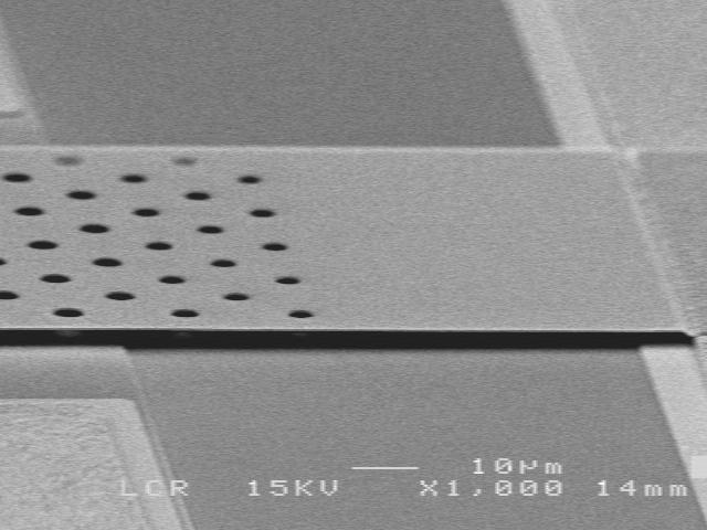
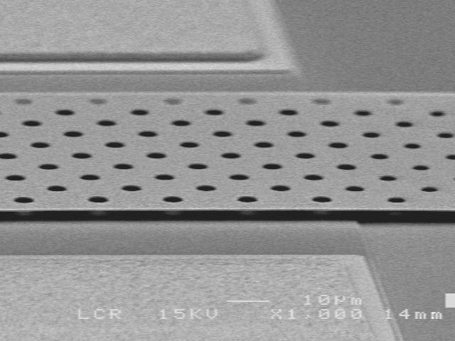
8 MEMS for Power Switching MEMS technology used : Surface micro-machining Au 3.6 µm TiW / Al 0.7 µm Si 3 N µm TiW/Au 0.6 µm SiO 2 2 µm Au CPW line W = 80 µm S = 120 µm Control electrode (TiW) Si HR or glass substrate Schematic of cross section (Shunt Switch) Holes are etched into the membrane in order to facilitate the membrane delivery 7
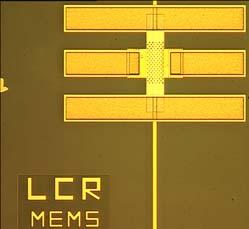
9 MEMS for Power Switching 120 µm 120 µm 80 µm 100 µm Control pad GND SGN GND 8


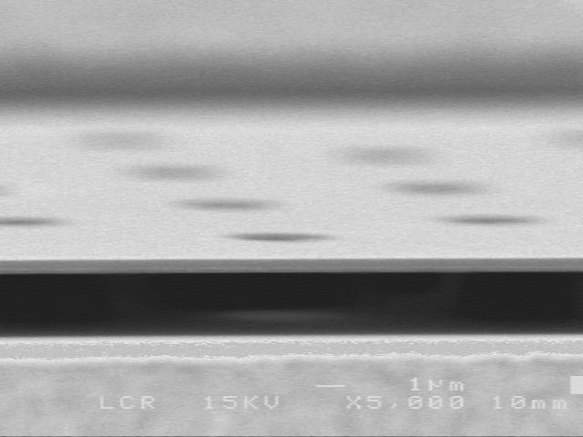
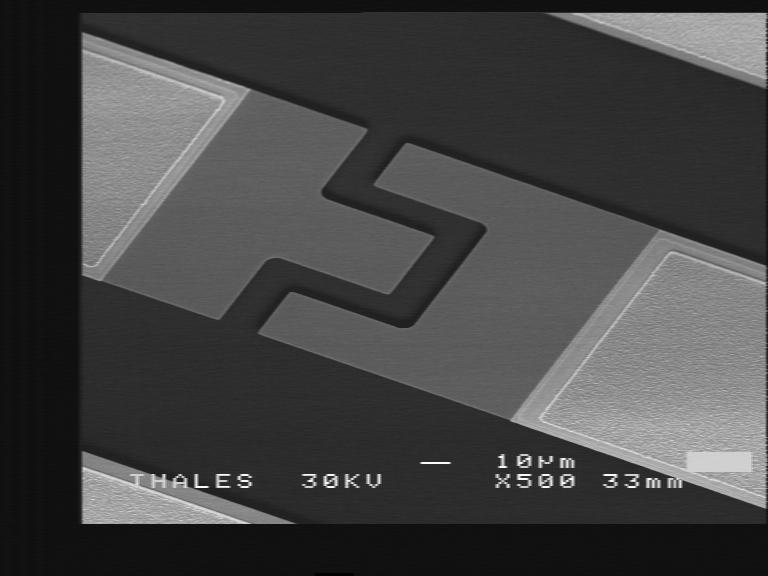
10 SEM pictures of fabricated switches Ground membrane command electrode gap signal RF in signal RF out membrane Ground Gap : g = 3 µm Membrane width : 100 µm Dielectric thickness : g 0 = 0.2 µm 9

11 10 SEM pictures of fabricated switches
12 11 Insertion losses (Membrane in up position) (20 GHz):S 12 : db (40 GHz):S 12 : -0.2 db ,05-0,1-0,15-0,2 Pertes A(dB) -0,25-0,3-0,35 F (GHz)
13 12 Isolation (Membrane in down position) 25 db à 40 GHz Isolation (db)
14 Return losses S 11 Membrane in up position (The membrane is unactuated ) (20 GHz):S 11 : 13 db (40 GHz):S 11 : 10 db GHz measurements S 11 Membrane in down position (The membrane is actuated) S11 (20 GHz):S 11 : 3 db (40 GHz):S 11 : 1 db
15 14 Thales results Results under 0dBm Key characteristics of TRT MEMS RF Switch Isolation 32 db (40 GHz) 18 db (20 GHz) Insertion losses 0.2 db (40 GHz) 0.1 db (20 GHz) Driving voltage V C on 2-3 pf C off ff R on < 2 Ohms Switching time < 5 µs K 81 N/m Mechanical resonance 214 khz
16 15 Line of command 120 plan de masse plan de masse V1 V2 High resistivity resistors Series MEMS switches Conception ON state : Membrane in down position OFF state : Membrane in up position V1 C C on off =109

17 16 SEM pictures of fabricated switches
18 17 How do we improve switch performance? Ground Signal Ground Bridge or membrane Dielectric Rf-On state (membrane Up) Rf-Off state (membrane Down) Increasing switching ratio ( C C on off ) Increasing C down for a given C up
19 18 Influence of K on switch isolation Simulations HFSS Isolation (db) f(ghz) Much higher isolation in DOWN state than previous design Replace Si 3 N 4 with high dielectric constant ZrO 2 film


20 19 SEM pictures of fabricated ZrO2 capacitive switch
21 20 Switch measured characteristics: Insertion loss Shunt ZrO 2 switch characteristics in the UP state 0-0,05-0,1-0,15 Diélectrique ZrO2 (Er = 22) -0,2-0,25 petes d'insertion Insertion loss (db) -0,3-0, fréquence Frequency (GHz)
22 21 Switch measured characteristics: Return loss Shunt ZrO 2 switch characteristics in the UP state Diélectrique ZrO2 (Er = 22) -40 adaptation Return loss (db) fréquence (GHz) Frequency (GHz)
23 22 Switch measured characteristics: Isolation Shunt ZrO 2 switch characteristics in the DOWN state Diélectrique ZrO2 (Er = 22) -40 Isolation isolation (db) fréquence Frequency (GHz)
24 23 Switch measured characteristics: Return loss Shunt ZrO 2 switch characteristics in the DOWN state 0-0,1-0,2-0,3-0,4-0,5 Diélectrique ZrO2 (Er = 22) -0,6-0,7-0,8 Return loss (db) reflexion -0, fréquence (GHz) Frequency (GHz)

25 Signal OUT1 24 MEMS SPDT Switch (ZrO2) Signal IN Signal OUT2 Coplanar Waveguide

26 25 Signal OUT 3 MEMS SPDT Switch (ZrO2) Signal IN 1 On Off Signal OUT 2 THALES design, Serial-serial PZT-PZT
 -10-15 -20 Magnitude (db) 1 3 2 S 33-25 26 S 33 in the on state (Membrane down position) -30 0 2 4 6 8 10 12 14 16 18 20 Frequency Fréquence")
27 MEMS SPDT Switch (ZrO2) without packaging (X band) 0-0,2-0,4-0,6 Membrane down position (S 13 in the on state) -0,8-1 -1,2-1,4 S 13 Magnitude (db) -1,6-1, Frequency Fréquence (GHz) Magnitude (db) S S 33 in the on state (Membrane down position) Frequency Fréquence (GHz)
28 27 MEMS SPDT Switch (ZrO2) without packaging (X band) Membrane up position (in the off state) S 12 Magnitude (db) , , Frequency Fréquence (GHz) -0,06-0,08 Magnitude (db) 1 S ,1-0,12 S 22 in the off state (Membrane up position) -0, Fréquence (GHz) Frequency (GHz)
29 MEMS SPDT Switch (ZrO2) without packaging (X band) 0-5 Membrane up position (in the off state) S S 23 Magnitude (db) Magnitude (db) Fréquence (GHz) Frequency (GHz) Frequency Fréquence (GHz) 28
30 29 Power handling measurements (10 GHz) Power Handling of RF MEMS Capacitive shunt switches GHz Synthesizer TWT-Amplifier DC Power supply Attenuator(1) Directional Coupler DC Bias Tee Spectrum Analyser Attenuator(2) RF Probe DUT Network Analyser Attenuator(4) Attenuator(3) RF Probe
31 30 Power Handling of RF MEMS Capacitive shunt switch PZT Shunt capacitive switch ISOLATION 30 db (10GHz) PERTES INSERTION 0.1dB (10GHz) TENSION D ACTIVATION 25~30Volts RAPPORT Con/Coff 150 GAP D AIR (entre membrane et diélectrique) 0.5 µm Al, 0.2µm TiW 2~2.5µm MEMBRANE 240µm x 100µm Cpw 80µm/120µm/80µm METALLISATION DE LA MEMBRANE CONSTANTE DIELECTRIQUE UTILISEE (PZT) 160~170 VSWR 1.2 Switching time 4 µs under 0dBm (10 GHz)
32 31 Power Handling of RF MEMS Capacitive shunt switch Measured down-state isolation versus input power at 10GHz Isolation (db) Power In (dbm)
33 32 Power Handling of RF MEMS Capacitive shunt switch Measured up-state Insertion Loss versus input power at 10GHz 0-0,05-0,1-0,15 Insertion Loss (db) -0,2-0, Power In (dbm)
34 33 Lifetime measurements (10 GHz) High power RF lifetime of THALES MEMS switch at 10GHz TWT-Amplifier PC-Labview GHz Synthesizer DC Power supply Attenuator(1) Directional Coupler DC Bias Tee Network Analyser Attenuator(2) RF Probe DUT Spectrum Analyser Attenuator(4) Attenuator(3) RF Probe Power Meter
35 34-0,06 RF lifetime of THALES MEMS switch at 10GHz Cold switching (37 dbm) Measured up-state Insertion Loss versus input power at 10GHz -0,07-0,08-0,09-0,1-0,11-0,12-0,13-0,14-0,15-0,16-0,17-0,18-0,19-0,2-0,21-0,22 1,00E+00 1,00E+01 1,00E+02 1,00E+03 1,00E+04 1,00E+05 1,00E+06 1,00E+07 1,00E+08 1,00E+09 1,00E+10 Cycles Insertion Loss (db)
36 35-33,5 RF lifetime of THALES MEMS switch at 10GHz Cold switching (37 dbm) Measured down-state isolation versus input power at 10GHz , , , , ,5 1,00E+00 1,00E+01 1,00E+02 1,00E+03 1,00E+04 1,00E+05 1,00E+06 1,00E+07 1,00E+08 1,00E+09 1,00E+10 Cycles Isolation (db)
37 36 RF lifetime of THALES MEMS switch at 10GHz RF Lifetime at 10 GHz 10 Billion Cycles at 37 dbm 32 Devices Tested at 36 dbm and Room Temp. 25 Devices Completed 10 Billion Cycles (Stopped Test) 6 Devices Completed 1 Billion Cycles (Stopped Test) 1 Device Failed at 0.72 Billion Cycles 8 KHz Cycle Rate 0.69 Billion Cycles/Day 10 Billion Cycles in 15 Days
 Nanoelectromechanical")

38 37 CNs switch J. E. Jang et al., Appl. Phys. Lett. 87, (2005) Nanoelectromechanical switches with vertically aligned carbon nanotubes Department of engineering, University of Cambridge

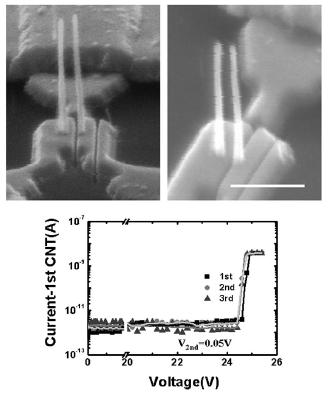
39 38 CNs switch
40 39 TRT Why carbon nanotube based NEMS? High isolation, low losses from MEMS properties Low actuation voltage < 10 V High switching speed ~ a few ns From nanometer size of CNs High power handling exceptional electrical and mechnical properties of CNs High integration density Low cost Low consumption Main difficulty Achieving reproducible and routinely fabrication process of CN switches


41 40 TRT TRT has developed a growth technology of highly homogeneous vertical CNs
42 41 This document and any data included are the property of Thales. They cannot be reproduced, disclosed or used without Thales' prior written approval. TRT Ohmic switch (metal/metal contact) Capacitive switch (metal/dielectric/metal contact)
43 42 TRT Coupling CNs with coplanar waveguides for RF switching
44 CN Antennas 43 Particular electrical properties: High characteristic impedance & high losses High relaxation frequency (>50GHz) High wave velocity (λ/50 - λ/100) Advantages of CN antennas: High integration High density circuits High frequency resonnators Applications of CN antennas: Wireless communications between nano-sized devices/organisms and macroscopic world Antenna arrays at high frequencies Thales: GHz Generator Dipole Radiated Field -λ/4 0 λ/4 Dipole Length I0 Current Distribution This document and any data included are the property of Thales. They cannot be reproduced, disclosed or used without Thales' prior written approval.


45 44 Technical issues: Dipole fabrication: FIB Impedance matching: 50Ω - 10kΩ Emission pattern measurements: Radiation efficiency 60 db CN Antennas
46 45 Conclusion Conclusion Key RF performance characteristics for a Zro 2 -SPDT switch are at 10 Ghz: insertion loss of 0.15 db and isolation of 28 db. RF lifetimes exceeding cycles achieved at input Power level of 36 dbm Research on nanotubes RF NEMS is underway at Thales
47 46 Thank you for your attention
48 47 Bare chip Characteristics: Insertion losses Membrane in up position 0-0,2-0,4-0,6-0,8-1 S12 pzt db -1,2-1,4-1,6-1, Freq GHz
49 GHz measurements db Return losses Freq GHz S11 pzt
50 49 0 Bare chip Characteristics: Isolation ( GHz) Membrane in down position S12 pzt db Freq GHz
51 GHz measurements 0-0,05-0,1 db -0,15-0,2-0,25 Return losses Freq GHz S11 pzt
High Power RF MEMS Switch Technology
 High Power RF MEMS Switch Technology Invited Talk at 2005 SBMO/IEEE MTT-S International Conference on Microwave and Optoelectronics Conference Dr Jia-Sheng Hong Heriot-Watt University Edinburgh U.K. 1
CARBON BASED SMART SYSTEM FOR WIRELESS APPLICATION
 CARBON BASED SMART SYSTEM FOR WIRELESS APPLICATION Start Date : 01/09/12 Project n 318352 Duration : 45 months Topic addressed : Very advanced nanoelectronic components: design, engineering, technology
SATURNE Microsystems Based on Wide Band Gap Materials for Future Space Transmitting Ultra Wideband Receiving Systems
 SATURNE Microsystems Based on Wide Band Gap Materials for Future Space Transmitting Ultra Wideband Receiving Systems A. ZIAEI THALES Research & Technology Research & Technology www.saturne-project.com
III-Nitride microwave switches Grigory Simin
 Microwave Microelectronics Laboratory Department of Electrical Engineering, USC Research Focus: - Wide Bandgap Microwave Power Devices and Integrated Circuits - Physics, Simulation, Design and Characterization
Design and Fabrication of Low-loss RF MEMS switches for a broadband reflectarray
 Design and Fabrication of Low-loss RF MEMS switches for a broadband reflectarray Afshin Ziaei (1), Thierry Dean (1), Michel Charrier (1), Paolo Bondavalli (1), Jean-philippe Polizzi (1) Hervé Legay (2),
Application Note 5525
 Using the Wafer Scale Packaged Detector in 2 to 6 GHz Applications Application Note 5525 Introduction The is a broadband directional coupler with integrated temperature compensated detector designed for
38050 Povo Trento (Italy), Via Sommarive 14 TIME CHARACTERIZATION OF CAPACITIVE MEMS RF SWITCHES
, Via Sommarive 14 TIME CHARACTERIZATION OF CAPACITIVE MEMS RF SWITCHES") UNIVERSITY OF TRENTO DEPARTMENT OF INFORMATION AND COMMUNICATION TECHNOLOGY 38050 Povo Trento (Italy), Via Sommarive 14 http://www.dit.unitn.it TIME CHARACTERIZATION OF CAPACITIVE MEMS RF SWITCHES G. Fontana,
UNIVERSITY OF TRENTO DEPARTMENT OF INFORMATION AND COMMUNICATION TECHNOLOGY 38050 Povo Trento (Italy), Via Sommarive 14 http://www.dit.unitn.it TIME CHARACTERIZATION OF CAPACITIVE MEMS RF SWITCHES G. Fontana,
INVENTION DISCLOSURE- ELECTRONICS SUBJECT MATTER IMPEDANCE MATCHING ANTENNA-INTEGRATED HIGH-EFFICIENCY ENERGY HARVESTING CIRCUIT
 INVENTION DISCLOSURE- ELECTRONICS SUBJECT MATTER IMPEDANCE MATCHING ANTENNA-INTEGRATED HIGH-EFFICIENCY ENERGY HARVESTING CIRCUIT ABSTRACT: This paper describes the design of a high-efficiency energy harvesting
CHAPTER 6 CARBON NANOTUBE AND ITS RF APPLICATION
 CHAPTER 6 CARBON NANOTUBE AND ITS RF APPLICATION 6.1 Introduction In this chapter we have made a theoretical study about carbon nanotubes electrical properties and their utility in antenna applications.
Integration of Optoelectronic and RF Devices for Applications in Optical Interconnect and Wireless Communication
 Integration of Optoelectronic and RF Devices for Applications in Optical Interconnect and Wireless Communication Zhaoran (Rena) Huang Assistant Professor Department of Electrical, Computer and System Engineering
77 GHz VCO for Car Radar Systems T625_VCO2_W Preliminary Data Sheet
 77 GHz VCO for Car Radar Systems Preliminary Data Sheet Operating Frequency: 76-77 GHz Tuning Range > 1 GHz Output matched to 50 Ω Application in Car Radar Systems ESD: Electrostatic discharge sensitive
Optically reconfigurable balanced dipole antenna
 Loughborough University Institutional Repository Optically reconfigurable balanced dipole antenna This item was submitted to Loughborough University's Institutional Repository by the/an author. Citation:
MICROWAVE MICROWAVE TRAINING BENCH COMPONENT SPECIFICATIONS:
 Microwave section consists of Basic Microwave Training Bench, Advance Microwave Training Bench and Microwave Communication Training System. Microwave Training System is used to study all the concepts of
Ordering Information. Specifications. RF MEMS Switch 2SMES-01. Contact Ratings. Terminal Arrangement. Actuator Ratings
 RF MEMS Switch Miniature, 10 GHz Band (typical) SPDT (transfer contacts) RF MEMS Switch Superior high-frequency characteristics at 10 GHz typical/8 GHz rated (50 Ω) Isolation of 30 db Insertion loss of
Limiter Diodes Features Description Chip Dimensions Model DOT Diameter (Typ.) Chip Number St l Style Inches 4 11
 Chip Number St l Style Inches 4 11") Features Low Loss kw Coarse Limiters 200 Watt Midrange Limiters 10 mw Clean Up Limiters 210 20 Description Alpha has pioneered the microwave limiter diode. Because all phases of manufacturing, from design
Features Low Loss kw Coarse Limiters 200 Watt Midrange Limiters 10 mw Clean Up Limiters 210 20 Description Alpha has pioneered the microwave limiter diode. Because all phases of manufacturing, from design
Study of MEMS Devices for Space Applications ~Study Status and Subject of RF-MEMS~
 Study of MEMS Devices for Space Applications ~Study Status and Subject of RF-MEMS~ The 26 th Microelectronics Workshop October, 2013 Maya Kato Electronic Devices and Materials Group Japan Aerospace Exploration
Figure 1 : Topologies of a capacitive switch The actuation voltage can be expressed as the following :
 ABSTRACT This paper outlines the issues related to RF MEMS packaging and low actuation voltage. An original approach is presented concerning the modeling of capacitive contacts using multiphysics simulation
MICROWAVE ENGINEERING-II. Unit- I MICROWAVE MEASUREMENTS
 MICROWAVE ENGINEERING-II Unit- I MICROWAVE MEASUREMENTS 1. Explain microwave power measurement. 2. Why we can not use ordinary diode and transistor in microwave detection and microwave amplification? 3.
MAAP Power Amplifier, 15 W GHz Rev. V1. Features. Functional Schematic. Description. Pin Configuration 2. Ordering Information
 Features 15 W Power Amplifier 42 dbm Saturated Pulsed Output Power 17 db Large Signal Gain P SAT >40% Power Added Efficiency Dual Sided Bias Architecture On Chip Bias Circuit 100% On-Wafer DC, RF and Output
INF5490 RF MEMS. L7: RF MEMS switches, I. S2008, Oddvar Søråsen Department of Informatics, UoO
 INF5490 RF MEMS L7: RF MEMS switches, I S2008, Oddvar Søråsen Department of Informatics, UoO 1 Today s lecture Switches for RF and microwave Examples Performance requirements Technology Characteristics
CMT2300AW Schematic and PCB Layout Design Guideline
 AN141 CMT2300AW Schematic and PCB Layout Design Guideline Introduction This document is the CMT2300AW Application Development Guideline. It will explain how to design and use the CMT2300AW schematic and
High Power PIN Diodes
 Applications Series/shunt elements in high power HF/VHF/ UHF transmit/receive (T/R) switches Features Very low thermal resistance for excellent power handling: 40 W C/W typical Low series resistance SMP1324-087LF:
Introduction: Planar Transmission Lines
 Chapter-1 Introduction: Planar Transmission Lines 1.1 Overview Microwave integrated circuit (MIC) techniques represent an extension of integrated circuit technology to microwave frequencies. Since four
Near-Field Scanning. Searching for Root Causes
 Near-Field Scanning Searching for Root Causes Feb. 06, 2018 Outline Susceptibility Scanning Conducted susceptibility: where does ESD current go? Near-field effects of electrostatic discharge events Emission
Parameter Frequency Typ Min (GHz)
") The is a broadband MMIC LO buffer amplifier that efficiently provides high gain and output power over a 20-55 GHz frequency band. It is designed to provide a strong, flat output power response when driven
The is a broadband MMIC LO buffer amplifier that efficiently provides high gain and output power over a 20-55 GHz frequency band. It is designed to provide a strong, flat output power response when driven
LOW LOSS FERROELECTRIC BASED PHASE SHIFTER FOR HIGH POWER ANTENNA SCAN BEAM SYSTEM
 LOW LOSS FERROELECTRIC BASED PHASE SHIFTER FOR HIGH POWER ANTENNA SCAN BEAM SYSTEM Franco De Flaviis and N.G. Alexopoulos University of California at Los Angeles, Dep. of Electrical Engineering Los Angeles
GaAs MMIC devices are susceptible to Electrostatic Discharge. Use proper ESD precautions when handling these items.
 The is a broadband, power efficient GaAs PHEMT distributed amplifier in a 4mm QFN surface mount package. The is designed to provide optimal LO drive for T3 mixers. Typically, ADM-26-2931SM provides. db
MEMS for RF, Micro Optics and Scanning Probe Nanotechnology Applications
 MEMS for RF, Micro Optics and Scanning Probe Nanotechnology Applications Part I: RF Applications Introductions and Motivations What are RF MEMS? Example Devices RFIC RFIC consists of Active components
Maxim Integrated Products 1
 19-0569; Rev 0; 5/06 MAX2041 Evaluation Kit General Description The MAX2041 evaluation kit (EV kit) simplifies the evaluation of the MAX2041 UMTS, DCS, and PCS base-station up/downconversion mixer. It
Signal Integrity Design of TSV-Based 3D IC
 Signal Integrity Design of TSV-Based 3D IC October 24, 21 Joungho Kim at KAIST joungho@ee.kaist.ac.kr http://tera.kaist.ac.kr 1 Contents 1) Driving Forces of TSV based 3D IC 2) Signal Integrity Issues
Signal Integrity Modeling and Measurement of TSV in 3D IC
 Signal Integrity Modeling and Measurement of TSV in 3D IC Joungho Kim KAIST joungho@ee.kaist.ac.kr 1 Contents 1) Introduction 2) 2.5D/3D Architectures with TSV and Interposer 3) Signal integrity, Channel
High-performance and Low-cost Capacitive Switches for RF Applications
 High-performance and Low-cost Capacitive Switches for RF Applications Bruce Liu University of California at Santa Barbara Toyon Research Corporation Toyon Research Corporation Fame Outline Motivation for
CHAPTER - 6 PIN DIODE CONTROL CIRCUITS FOR WIRELESS COMMUNICATIONS SYSTEMS
 CHAPTER - 6 PIN DIODE CONTROL CIRCUITS FOR WIRELESS COMMUNICATIONS SYSTEMS 2 NOTES 3 INTRODUCTION PIN DIODE CONTROL CIRCUITS FOR WIRELESS COMMUNICATIONS SYSTEMS Chapter 6 discusses PIN Control Circuits
Body-Biased Complementary Logic Implemented Using AlN Piezoelectric MEMS Switches
 University of Pennsylvania From the SelectedWorks of Nipun Sinha 29 Body-Biased Complementary Logic Implemented Using AlN Piezoelectric MEMS Switches Nipun Sinha, University of Pennsylvania Timothy S.
7-12GHz LNA. GaAs Monolithic Microwave IC. S21 (db)
") S21 (db) NF (db) GaAs Monolithic Microwave IC Description The is a monolithic two-stages wide band low noise amplifier circuit. It is self-biased. It is designed for military, space and telecommunication
S21 (db) NF (db) GaAs Monolithic Microwave IC Description The is a monolithic two-stages wide band low noise amplifier circuit. It is self-biased. It is designed for military, space and telecommunication
Application Note 5468
 GA-43228 High Linearity Wireless Data Power Amplifier for 2.3 to 2.5 GHz Applications Application Note 5468 Introduction This application note describes the GA-43228 power amplifier and gives actual performance
RF/Microwave Circuits I. Introduction Fall 2003
 Introduction Fall 03 Outline Trends for Microwave Designers The Role of Passive Circuits in RF/Microwave Design Examples of Some Passive Circuits Software Laboratory Assignments Grading Trends for Microwave
Application Note 1330
 HMPP-3865 MiniPAK PIN Diode High Isolation SPDT Switch Design for 1.9 GHz and 2.45 GHz Applications Application Note 133 Introduction The Avago Technologies HMPP-3865 parallel diode pair combines low inductance,
MASW P. SURMOUNT PIN Diode Switch Element with Thermal Terminal. Features. Description. Ordering Information 2.
 Features Specified Bandwidth: 45MHz 2.5GHz Useable 30MHz to 3.0GHz Low Loss 40dB High C.W. Incident Power, 50W at 500MHz High Input IP3, +66dBm @ 500MHz Unique Thermal Terminal for
AWS5504 GaAs IC Negative Control SPDT Reflective Switch DC-2.0 GHz Data Sheet - Rev 2.1
 GaAs IC Negative Control SPDT Reflective Switch DC2.0 GHz FEATURES High Linearity (IP3 48 dbm @ 0.9 GHz) Low Insertion Loss (0.4 db @ 0.9 GHz) 2.75 V to 3.5 to +2.75 operation Low DC Power Consumption
GaAs MMIC devices are susceptible to Electrostatic Discharge. Use proper ESD precautions when handling these items.
 ADM-26-931SM The ADM-26-931SM is a broadband, power efficient GaAs PHEMT distributed amplifier in a 4mm QFN surface mount package. The ADM-26-931SM is designed to provide optimal LO drive for T3 mixers.
Parameter Frequency Typ (GHz) See page 7 for minimum performance specs of AMM7602UC connectorized modules. Description Green Status
 See page 7 for minimum performance specs of AMM7602UC connectorized modules. Description Green Status") The is a broadband MMIC LO buffer amplifier that efficiently provides high gain and output power over a 20-55 GHz frequency band. It is designed to provide a strong, flat output power response when driven
The is a broadband MMIC LO buffer amplifier that efficiently provides high gain and output power over a 20-55 GHz frequency band. It is designed to provide a strong, flat output power response when driven
GaAs MMIC devices are susceptible to Electrostatic Discharge. Use proper ESD precautions when handling these items.
 ADM-12-931SM The ADM-12-931SM is a small, low power, and economical T3 driver or T3A pre-amplifier. It is a GaAs PHEMT distributed amplifier in a 3mm QFN surface mount package. The ADM-12-931SM can provide
Data Sheet. VMMK GHz Positive Gain Slope Low Noise Amplifier in SMT Package. Features. Description
 VMMK-3603 1-6 GHz Positive Gain Slope Low Noise Amplifier in SMT Package Data Sheet Description The VMMK-3603 is a small and easy-to-use, broadband, positive gain slope low noise amplifier operating in
EM Design of Broadband RF Multiport Toggle Switches
 EM Design of Broadband RF Multiport Toggle Switches W. Simon 1, B. Schauwecker 2, A. Lauer 1, A. Wien 1 and I. Wolff, Fellow IEEE 1 1 IMST GmbH, Carl-Friedrich-Gauss-Str. 2, 47475 Kamp Lintfort, Germany
GHz Voltage Variable Attenuator (Absorptive)
") Rev.. February 27.5-2.GHz Voltage Variable Attenuator (Absorptive) Features Single Positive Voltage Control: to +5V. 3dB Attenuation Range Low Insertion Loss I/O VSWR
Rev.. February 27.5-2.GHz Voltage Variable Attenuator (Absorptive) Features Single Positive Voltage Control: to +5V. 3dB Attenuation Range Low Insertion Loss I/O VSWR
Surface-mounted MEMS Switch
 Surface-mounted MEMS Switch Surface-mounted, ultracompact SPDT MEMS switch usable up to 10-GHz band (typical). Exceptional high-frequency characteristics in a broad spectrum up to 10 GHz (typical) At 8
HMPP-386x Series MiniPak Surface Mount RF PIN Diodes
 HMPP-86x Series MiniPak Surface Mount RF PIN Diodes Data Sheet Description/Applications These ultra-miniature products represent the blending of Avago Technologies proven semiconductor and the latest in
Maxim Integrated Products 1
 9-92; Rev 0; /0 MAX2242 Evaluation Kit General Description The MAX2242 evaluation kit (EV kit) simplifies evaluation of the MAX2242 power amplifier (PA), which is designed for 2.4GHz ISM-band direct-sequence
RF MEMS Impedance Tuners for 6 24 GHz Applications
 PUBLICATION P3 RF MEMS Impedance Tuners for 6 24 GHz Applications Accepted for publication to International Journal of RF and Microwave Computer-Aided Engineering, February 2006. Reprinted with permission
A RECONFIGURABLE HYBRID COUPLER CIRCUIT FOR AGILE POLARISATION ANTENNA
 A RECONFIGURABLE HYBRID COUPLER CIRCUIT FOR AGILE POLARISATION ANTENNA F. Ferrero (1), C. Luxey (1), G. Jacquemod (1), R. Staraj (1), V. Fusco (2) (1) Laboratoire d'electronique, Antennes et Télécommunications
Modeling and Simulation of Via Conductor Losses in Co-fired Ceramic Substrates Used In Transmit/Receive Radar Modules
 Modeling and Simulation of Via Conductor Losses in Co-fired Ceramic Substrates Used In Transmit/Receive Radar Modules 4/5/16 Rick Sturdivant, CTO 310-980-3039 rick@rlsdesigninc.com Edwin K.P. Chong, Professor
Micro- and nano-scale switches and tuning elements for microwave applications
 University of South Florida Scholar Commons Graduate Theses and Dissertations Graduate School 26 Micro- and nano-scale switches and tuning elements for microwave applications Thomas P. Ketterl University
Preliminary Product Overview
 Preliminary Product Overview Features DC to > 3 GHz Frequency Range 25 Watt (CW), 200W (Pulsed) Max Power Handling Low On-State Insertion Loss, typical 0.3 db @ 3 GHz Low On-State Resistance < 0.75 Ω 25dB
RF(Radio Frequency) MEMS (Micro Electro Mechanical
 MEMS (Micro Electro Mechanical") Design and Analysis of Piezoelectrically Actuated RF-MEMS Switches using PZT and AlN PrashantTippimath M.Tech., Scholar, Dept of ECE M.S.Ramaiah Institute of Technology Bengaluru tippimathprashant@gmail.com
Design and Analysis of Piezoelectrically Actuated RF-MEMS Switches using PZT and AlN PrashantTippimath M.Tech., Scholar, Dept of ECE M.S.Ramaiah Institute of Technology Bengaluru tippimathprashant@gmail.com
RF Test Accessories. Antenna Coupler. TC-93010C fitted with F930102A TC-93013A. Frequency Range : 820 ~ 960 MHz. Frequency Range : 0.
 RF Test Accessories Antenna Coupler TC-93010C Tubular Type Antenna Coupler Frequency Range : 0.8 ~ 2GHz RF Connector : SMA(f) Weight : 60g Patent Pending # 2001-24403 Hole Size : 11mm TC-93010C fitted
MPS S & MPS S CONTROL DEVICE MONOLITHIC SPST PIN RoHS Compliant
 GENERAL DESCRIPTION The MPS4101 012S and MPS4102 013S are a single chip silicon monolithic series/shunt element. The parasitic inductance is minimized in this design resulting in wide band, low loss, high
Preliminary. MM7100 High-Voltage SPST Digital-Micro-Switch. Product Overview PRELIMINARY DATA SHEET, SEE PAGE 11 FOR DETAILS
 MM7100 High-Voltage SPST Digital-Micro-Switch Product Overview Features: Frequency Range: DC to 750 MHz Low On-State Resistance < 0.30Ω (typ.) Rated Voltage (AC or DC): 400V Rated Current (AC or DC): 2A
ISSCC 2006 / SESSION 10 / mm-wave AND BEYOND / 10.1
 10.1 A 77GHz 4-Element Phased Array Receiver with On-Chip Dipole Antennas in Silicon A. Babakhani, X. Guan, A. Komijani, A. Natarajan, A. Hajimiri California Institute of Technology, Pasadena, CA Achieving
30dB P IN =25dBm. 0.50dB P IN =25dBm. 33dB P IN =25dBm. 21dB
 NJG1HA8 SPDT SWITCH GaAs MMIC GENERAL DESCRIPTION The NJG1HA8 is a GaAs SPDT switch IC suited for antenna switch of WiMAX application and other wireless handsets. The NJG1HA8 features high power handling,
A 3.9 ns 8.9 mw 4 4 Silicon Photonic Switch Hybrid-Integrated with CMOS Driver
 A 3.9 ns 8.9 mw 4 4 Silicon Photonic Switch Hybrid-Integrated with CMOS Driver A. Rylyakov, C. Schow, B. Lee, W. Green, J. Van Campenhout, M. Yang, F. Doany, S. Assefa, C. Jahnes, J. Kash, Y. Vlasov IBM
Fourth Year Antenna Lab
 Fourth Year Antenna Lab Name : Student ID#: Contents 1 Wire Antennas 1 1.1 Objectives................................................. 1 1.2 Equipments................................................ 1
MA4AGSW2. AlGaAs SP2T PIN Diode Switch. MA4AGSW2 Layout. Features. Description. Absolute Maximum Ratings TA = +25 C (Unless otherwise specified)
") AlGaAs SP2T PIN Diode Switch Features Ultra Broad Bandwidth: 5 MHz to 5 GHz Functional bandwidth : 5 MHz to 7 GHz.7 db Insertion Loss, 33 db Isolation at 5 GHz Low Current consumption: -1 ma for Low Loss
AlGaAs SP2T PIN Diode Switch Features Ultra Broad Bandwidth: 5 MHz to 5 GHz Functional bandwidth : 5 MHz to 7 GHz.7 db Insertion Loss, 33 db Isolation at 5 GHz Low Current consumption: -1 ma for Low Loss
Data Sheet. VMMK GHz Directional Detector in SMT Package. Features. Description. Specifications (4 GHz, Vb = 1.5 V, Zin = Zout = 50 Ω)
") VMMK-3113 2-6 GHz Directional Detector in SMT Package Data Sheet Description The VMMK-3113 is a small and easy-to-use, broadband, directional detector operating in various frequency bands from 2 to 6 GHz
VMMK-3113 2-6 GHz Directional Detector in SMT Package Data Sheet Description The VMMK-3113 is a small and easy-to-use, broadband, directional detector operating in various frequency bands from 2 to 6 GHz
Power Reduction in RF
 Power Reduction in RF SoC Architecture using MEMS Eric Mercier 1 RF domain overview Technologies Piezoelectric materials Acoustic systems Ferroelectric materials Meta materials Magnetic materials RF MEMS
Micro-sensors - what happens when you make "classical" devices "small": MEMS devices and integrated bolometric IR detectors
 Micro-sensors - what happens when you make "classical" devices "small": MEMS devices and integrated bolometric IR detectors Dean P. Neikirk 1 MURI bio-ir sensors kick-off 6/16/98 Where are the targets
Development of High C on C off Ratio RF MEMS Shunt Switches
 ROMANIAN JOURNAL OF INFORMATION SCIENCE AND TECHNOLOGY Volume 11, Number 2, 2008, 143 151 Development of High C on C off Ratio RF MEMS Shunt Switches F. GIACOMOZZI 1, C. CALAZA 1, S. COLPO 1, V. MULLONI
Pin Connections and Package Marking. GUx
 Surface Mount RF PIN Switch Diodes Technical Data HSMP-389x Series HSMP-89x Series Features Unique Configurations in Surface Mount Packages Add Flexibility Save Board Space Reduce Cost Switching Low Capacitance
HMC-AUH232 MICROWAVE & OPTICAL DRIVER AMPLIFIERS - CHIP. GaAs HEMT MMIC MODULATOR DRIVER AMPLIFIER, DC - 43 GHz. Typical Applications.
 DRIVER AMPLIFIER, DC - 3 GHz Typical Applications This is ideal for: 0 Gb/s Lithium Niobate/ Mach Zender Fiber Optic Modulators Broadband Gain Block for Test & Measurement Equipment Broadband Gain Block
An on-chip antenna integrated with a transceiver in 0.18-µm CMOS technology
 This article has been accepted and published on J-STAGE in advance of copyediting. Content is final as presented. IEICE Electronics Express, Vol.* No.*,*-* An on-chip antenna integrated with a transceiver
FEATURES DESCRIPTION ABSOLUTE MAXIMUM RATINGS. T AMB = +25 C ( Unless otherwise specified )
") Monolithic PIN SP5T Diode Switch FEATURES Ultra Broad Bandwidth: 50MHz to 26GHz 1.0 db Insertion Loss 30 db Isolation at 20GHz Reliable. Fully Monolithic Glass Encapsulated Construction DESCRIPTION The
Monolithic PIN SP5T Diode Switch FEATURES Ultra Broad Bandwidth: 50MHz to 26GHz 1.0 db Insertion Loss 30 db Isolation at 20GHz Reliable. Fully Monolithic Glass Encapsulated Construction DESCRIPTION The
Transmitarrays, reflectarrays and phase shifters for wireless communication systems. Pablo Padilla de la Torre Universidad de Granada
 Transmitarrays, reflectarrays and phase shifters for wireless communication systems Pablo Padilla de la Torre Universidad de Granada Outline 1. Introduction to Transmitarray and Reflectarray structures
Design and Simulation of RF MEMS Capacitive type Shunt Switch & its Major Applications
 IOSR Journal of Electronics and Communication Engineering (IOSR-JECE) e-issn: 2278-2834, p- ISSN: 2278-8735. Volume 4, Issue 5 (Jan. - Feb. 2013), PP 60-68 Design and Simulation of RF MEMS Capacitive type
W-band Mixer. GaAs Monolithic Microwave IC
 W-band Mixer GaAs Monolithic Microwave IC Description The CHM2179b98F is a monolithic single channel mixer, which integrates high quality Schottky diodes that produces low conversion loss and very low
RF Discrete Devices Designer Kit
 RF Discrete Devices Designer Kit The Easier, Faster Way to Design Quality RF Solutions Skyworks Solutions is committed to making your RF designs easier than ever. This design kit includes 5-10 components
Design and Fabrication of RF MEMS Switch by the CMOS Process
 Tamkang Journal of Science and Engineering, Vol. 8, No 3, pp. 197 202 (2005) 197 Design and Fabrication of RF MEMS Switch by the CMOS Process Ching-Liang Dai 1 *, Hsuan-Jung Peng 1, Mao-Chen Liu 1, Chyan-Chyi
100 MHz to 4000 MHz RF/IF Digitally Controlled VGA ADL5240
 1 MHz to 4 MHz RF/IF Digitally Controlled VGA ADL524 FEATURES Operating frequency from 1 MHz to 4 MHz Digitally controlled VGA with serial and parallel interfaces 6-bit,.5 db digital step attenuator 31.5
Compact Multilayer Hybrid Coupler Based on Size Reduction Methods
 Progress In Electromagnetics Research Letters, Vol. 51, 1 6, 2015 Compact Multilayer Hybrid Coupler Based on Size Reduction Methods Young Kim 1, * and Youngchul Yoon 2 Abstract This paper presents a compact
CMT211xA Schematic and PCB Layout Design Guideline
 AN101 CMT211xA Schematic and PCB Layout Design Guideline 1. Introduction The purpose of this document is to provide the guidelines to design a low-power CMT211xA transmitter with the maximized output power,
Advanced Information: AI1714. DC-14GHz Voltage Variable Attenuator. GaAs Monolithic Microwave IC
 AI1714 : AI1714 GaAs Monolithic Microwave IC UMS develops a Voltage Variable Attenuator (VVA) in leadless surface mount hermetic metal ceramic 6x6mm² package, which operates from DC to 14GHz. This device,
GaAs MMIC devices are susceptible to Electrostatic Discharge. Use proper ESD precautions when handling these items.
 ADM-26-929SM The ADM-26-929SM is a broadband, efficient GaAs PHEMT distributed amplifier in a 4mm QFN surface mount package. It is designed to provide optimal LO drive for T3 mixers and offers 13 db typical
High Isolation SPDT SWITCH
 High Isolation SPDT SWITCH GENERAL DESCRIPTION The NJG1697EM1 is a 1bit control GaAs high isolation SPDT switch MMIC. The NJG1697EM1 features very high isolation and low control voltage. It has integrated
Broadband analog phase shifter based on multi-stage all-pass networks
 This article has been accepted and published on J-STAGE in advance of copyediting. Content is final as presented. IEICE Electronics Express, Vol.* No.*,*-* Broadband analog phase shifter based on multi-stage
Surface Mount SOT-363 (SC-70) Package. Pin Connections and Package Marking GND. V dd. Note: Package marking provides orientation and identification.
 Package. Pin Connections and Package Marking GND. V dd. Note: Package marking provides orientation and identification.") GHz V Low Current GaAs MMIC LNA Technical Data MGA-876 Features Ultra-Miniature Package.6 db Min. Noise Figure at. GHz. db Gain at. GHz Single + V or V Supply,. ma Current Applications LNA or Gain Stage
GHz V Low Current GaAs MMIC LNA Technical Data MGA-876 Features Ultra-Miniature Package.6 db Min. Noise Figure at. GHz. db Gain at. GHz Single + V or V Supply,. ma Current Applications LNA or Gain Stage
AT General Purpose, Low Current NPN Silicon Bipolar Transistor. Data Sheet
 AT-4532 General Purpose, Low Current NPN Silicon Bipolar Transistor Data Sheet Description Avago s AT-4532 is a general purpose NPN bipolar transistor that has been optimized for maximum f t at low voltage
Spontaneous Hyper Emission: Title of Talk
 Spontaneous Hyper Emission: Title of Talk Enhanced Light Emission by Optical Antennas Ming C. Wu University of California, Berkeley A Science & Technology Center Where Our Paths Crossed Page Nanopatch
EC 1402 Microwave Engineering
 SHRI ANGALAMMAN COLLEGE OF ENGINEERING & TECHNOLOGY (An ISO 9001:2008 Certified Institution) SIRUGANOOR,TRICHY-621105. DEPARTMENT OF ELECTRONICS AND COMMUNICATION ENGINEERING EC 1402 Microwave Engineering
DC-12 GHz Tunable Passive Gain Equalizer
 DC-12 GHz Tunable Passive Gain Equalizer AMT1753011 Features Frequency Range : DC-12 GHz 6 db insertion loss Tunable gain slope (+0.5dB/GHz to -0.2 db/ghz) Input Return Loss > 8 db Output Return Loss >
Advanced RF MEMS CAMBRIDGE UNIVERSITY PRESS. Edited by STEPAN LUCYSZYN. Imperial College London
 Advanced RF MEMS Edited by STEPAN LUCYSZYN Imperial College London n CAMBRIDGE UNIVERSITY PRESS Contents List of contributors Preface List of abbreviations page xiv xvii xx Introduction 1 1.1 Introduction
SUPPLEMENTARY INFORMATION
 Room-temperature continuous-wave electrically injected InGaN-based laser directly grown on Si Authors: Yi Sun 1,2, Kun Zhou 1, Qian Sun 1 *, Jianping Liu 1, Meixin Feng 1, Zengcheng Li 1, Yu Zhou 1, Liqun
Application Note No. 025
 Application Note, Rev. 2.0, Oct. 2006 Application Note No. 025 1400-1600 MHz PIN-Diode Transmit-Receive Switch RF & Protection Devices Edition 2006-10-20 Published by Infineon Technologies AG 81726 München,
GHz 6-Bit Digital Attenuator
 .5 1.5 GHz 6-Bit Digital Attenuator Features Frequency Range :.5 to 1.5 GHz 31.5dB Attenuation Range 5.2dB Insertion loss max..5db RMS attenuation error 23 max. phase variation 1.6:1 Input\Output VSWR
BROADBAND DISTRIBUTED AMPLIFIER
 ADM-126-83SM The ADM-126-83SM is a broadband, efficient GaAs PHEMT distributed amplifier with an integrated bias tee in a 4mm QFN surface mount package, designed to provide efficient LO drive for T3 mixers.
Data Sheet. VMMK GHz Directional Detector in SMT Package. Features. Description. Specifications (35 GHz, Vb = 1.5 V, Zin = Zout = 50 Ω)
") VMMK-3413 25-45 GHz Directional Detector in SMT Package Data Sheet Description The VMMK-3413 is a small and easy-to-use, broadband, directional detector operating in various frequency bands from 25 to
VMMK-3413 25-45 GHz Directional Detector in SMT Package Data Sheet Description The VMMK-3413 is a small and easy-to-use, broadband, directional detector operating in various frequency bands from 25 to
Low Actuation Wideband RF MEMS Shunt Capacitive Switch
 Available online at www.sciencedirect.com Procedia Engineering 29 (2012) 1292 1297 2012 International Workshop on Information and Electronics Engineering (IWIEE) Low Actuation Wideband RF MEMS Shunt Capacitive
RF applications of PIN diodes
 From the SelectedWorks of Chin-Leong Lim June 24, 2008 RF applications of PIN diodes Chin-Leong Lim Available at: https://works.bepress.com/chin-leong_lim/9/ RF Applications of PIN diodes IEEE MTT-ED-SSCS
Parameter Min Typ Max Units Frequency Range
 Features Low loss broadband performance High isolation Fast switching speed Non-reflective design Small die size Functional Block Diagram B A 3 4 5 2 RFC A B 6 Description The CMD196 is a general purpose
CHX2090-QDG RoHS COMPLIANT
 RoHS COMPLIANT Description GaAs Monolithic Microwave IC in SMD leadless package The CHX2090-QDG is a cascadable frequency doubler monolithic circuit, which integrate an output buffer amplifier that produces
Silicon PIN Limiter Diodes V 5.0
 5 Features Lower Insertion Loss and Noise Figure Higher Peak and Average Operating Power Various P1dB Compression Powers Lower Flat Leakage Power Reliable Silicon Nitride Passivation Description M/A-COM
4.1.2 InAs nanowire circuits fabricated by field-assisted selfassembly on a host substrate
 22 Annual Report 2010 - Solid-State Electronics Department 4.1.2 InAs nanowire circuits fabricated by field-assisted selfassembly on a host substrate Student Scientist in collaboration with R. Richter