State of the art and perspectives of CMOS avalanche detectors
|
|
|
- Gary Bryan
- 5 years ago
- Views:
Transcription
1 State of the art and perspectives of CMOS avalanche detectors Lucio Pancheri DII, University of Trento & TIFPA-INFN, Italy CERN seminar January 20, 2017

2 Research on silicon detectors in Trento FBK Clean room UniTN Dept. Physics INFN-TIFPA UniTN Dept. Industrial Engineering

3 Proton therapy TIFPA FBK UniTN
4 Outline Introduction CMOS-integrated single-photon detectors: an overview APiX: Geiger-mode avalanche pixel detectors for ionizing particles Conclusion and future perspectives 4
5 Geiger-mode avalanche detectors a.k.a. Single-Photon Avalanche Diodes (SPADs), SiPM cell V BIAS > V BD SPAD I SPAD Quenching V EX Avalanche triggering R Q VB V BIAS V SPAD Recharging 5
6 Geiger-mode avalanche detectors V BIAS > V BD Vout 1 primary generated electron-hole pair: very large current pulse ~ electrons SPAD Vout V EX R Q events time 6
7 CMOS SPAD characteristics Features: Single-photon sensitivity shot noise limited Excellent timing resolution: ~100 ps FWHM CMOS: Monolithic integration of SPAD and processing electronics Arrays single-photon imaging 7
8 Outline Introduction CMOS-integrated single-photon detectors: an overview APiX: Geiger-mode avalanche pixel detectors for ionizing particles Conclusion and future perspectives 8


9 CMOS SPADs: early example at EPFL Process: CMOS 0.8μm Area: 30μm 2 Peak PDE: 20% DCR: 300 Hz Timing resolution: 50 ps FWHM A. Rochas et al., Proc. SPIE

10 CMOS SPADs: deep submicron Process: CMOS 130 nm Area: 50μm 2 Peak PDE: 33% DCR: 40 Hz Timing resolution: 237 ps FWHM J. Richardson et al., IEEE Trans. Electron Dev

11 CMOS SPADs: high efficiency Process: CMOS 350nm Imaging with custom implantation Area: 700μm 2 Peak PDE: > 50% DCR: 50 Hz Timing resolution: 142 ps FWHM D. Bronzi et al., Proc. IEEE ESSDERC
12 Summary and comparison with SiPM SiPM: For major manufacturers PDE > 70% (single cell, not considering FF) DCR ~ 50 khz/mm 2 With customization, CMOS can approach SiPM performance For a complete overview, see D. Bronzi, et al., IEEE Sensors J
13 SPAD array applications Time-Of-Flight optical ranging, LIDAR Fluorescence spectroscopy Raman spectroscopy Gamma ray detection (PET) Quantum cryptography 13


14 Time-of-Flight optical ranging Automotive LIDAR developed by Toyota 180nm CMOS SPAD array with integrated TDCs 70% array Fill Factor Distance range: 100 m C. Niclass et al., IEEE J. Solid-State Circuits,


15 Fluorescence microscopy Multi-parametric fluorescence imaging 350nm CMOS (AMS) 4-line SPAD array Sub-ns gated counters 36% Fill Factor Intensity Color Lifetime Label-free imaging of unstained liver tissue excised from a tumorogenic murine model M. Popleteeva et al., Opt. Expr,
 130nm CMOS")
 integrated TDCs")

16 Digital SiPMs for PET SPADNET project (EU FP7) 130nm CMOS process Large pixels including 180 SPADs (Mini-SiPM) integrated TDCs 42.6 % pixel Fill Factor L. Braga et al., IEEE J. Solid-State Circuits,


")
17 First consumer products: ST ToF sensor Proximity sensor based on SPAD array and pulsed VCSEL Presented in 2014 Mobile applications (mounted on iphone7) Low power Short range (15 cm) 17

18 SPAD image sensor MegaFrame EU project (FP6) C. Veerappan et al., ISSCC x 128 pixel array Technology: 130nm CMOS In-pixel Time-to-Digital Conv. 140ps timing resolution Pixel pitch: 50um Fill factor: 1% 18


19 Improving the Fill Factor 16μm x 16μm pixel 65nm CMOS binary pixel (7 transistors) SPAD deep nwell sharing Improved SPAD GR 61% Fill Factor I. Gyongy et al., IEDM

20 Deep APD Panasonic project 110nm CMOS Backside illumination Avalanche multiplication region below electronics Pixel pitch 3.8μm 4 transistors / pixel Linear and binary mode M. Mori et al., ISSCC
 electroiq.")
21 3D integration High density interconnections successfully demonstrated for image sensors Sony 13 Mpixel stacked image sensor (2013) electroiq.com 21
 B. Aull et al., IEEE Sensors J.")
22 3D-integrated SPAD image sensor 1 MIT Lincoln Laboratory 25μm pitch 180nm CMOS + custom (APDs) 7-bit counter/pixel Backside illumination 10-20% detection efficiency (limited by optical cross-talk) B. Aull et al., IEEE Sensors J.,
23 3D-integrated SPAD image sensor μm pitch 65nm CMOS (top) + 40nm CMOS (bottom) 2 6-bit counters/pixel Backside illumination 45% Fill Factor T. Al Abbas et al., IEDM
24 Outline Introduction CMOS-integrated single-photon detectors: an overview APiX: Geiger-mode avalanche pixel detectors for ionizing particles Conclusion and future perspectives 24

25 APiX particle detector concept Quenching Discriminators Particle detection Coincidence detector Dark counts Two Geiger-mode avalanche detectors in coincidence: DCR = DCR 1 x DCR 2 x 2DT In-pixel coincidence: integrated electronics is needed: CMOS avalanche detectors V. Saveliev, US Patent. 8,269,181, 2012 N. D Ascenzo et al., JINST

26 SPADs in 150nm CMOS process Standard CMOS process no modifications Avalanche diodes in deep nwell: isolated from substrate Type 1: Shallow step junction Active thickness ~ 1μm Type2: Deep graded junction Active thickness ~ 1.5μm L. Pancheri, D. Stoppa, ESSDERC
27 Detection probability [%] Photo-Detection Efficiency Type 1: p+/nwell 40 Type 2: pwell/niso VE = 3V VE = 4V VE = 5V VE = 6V Wavelength [nm] Shallower junction: better NUV Blue efficiency Wider depletion region: Better red-ir efficiency L. Pancheri et al., J. Selected Topics in Quantum Electron,
28 Counts Single-photon timing resolution Counts Measured on 10-μm devices, with blue laser (470nm), 70ps FWHM Type pwell/niso 1: 60ps FWHM p+/nwell Type pwell/niso 2: 170ps FWHM FWHM = 184ps 92ps FW(M/100) = ps ps FWHM = 184ps FW(M/100) = 1170 ps Time [ns] Time [ns] 28
29 Proof-of-concept demonstrator 2-layer pixel cross section: Electronic readout on both layers Metal shielding from optical cross-talk Vertical interconnection by bump bonding 29

30 Pixel architecture High voltage V bspad applied at nwell Maximum voltage at node A: V ov = V bspad V BD Small capacitance at node A Passive quenching with constant current recharge 30

31 Pixel architecture Front-end transistors: 3.3V Maximum overvoltage 3.3V Digital circuitry: 1.8V compact fast low-power 31

32 Pixel architecture: enable register Pixels can be individually disabled: M 2 disables recharge Output and gate blocks output pulses 32

33 Pixel architecture: coincidence Coincidence with top-layer pixel 33

34 Pixel architecture: coincidence Real coincidence Accidental coincidence 34

35 Pixel architecture: monostable Pulse shortening: reduces the rate of accidental coincidence Programmable pulse width: 750ps, 1.5ns, 10ns 35

36 Pixel architecture: storage Global shutter operation: Fast transfer from memory to output register Simultaneous accumulation and data output 36

37 2-level pixel schematic Top pixel: subset of bottom pixel 37

 pixels")
38 Sensor architecture: row-wise OR Test output outor: combination of all the active (enabled) pixels in the row 38


39 Row-wise coincidence circuit Test coincidence in the sensor plane m and n can be arbitrarily selected 39


40 Sensor floorplan Bottom chip Top chip Wire bonding pads on chip 2: pre-integration test. Top chip Bottom chip Final assembly 40

 Pixels with shielded")
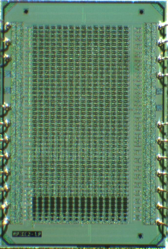
41 Pixel array 16 x 48 pixel array Pixel size: 50μm x 75μm Splittings in detector type and area Bump bonding pad 30μm x 30μm 35μm x 35μm 40μm x 40μm 43μm x 45μm Pixels with different detector area (unshielded) Pixels with shielded detectors 41


42 Bottom chip - Micrographs Shielded Unshielded 42

43 Sensor micrographs Bottom chip Top chip 43
44 Experimental results - summary Characterization of single-layer sensors: Core supply current (at 1.8V): 8mA Breakdown voltage uniformity Dark count rate In-plane coincidence Timing resolution Cross-talk Vertically integrated sensors with bump bonding (IZM): Coincidence dark counts Test with beta source Test beam 44
45 Breakdown voltage uniformity Measurements on 5 sample chips x 2 types x 196 devices per chip Very good uniformity on-chip (s < 20mV) Large difference (1V) between different chips for type 1 45
46 DCR distribution Active area: 43μm x 45μm DCR distribution spans 2 orders of magnitude at RT Median value at 20 C: 2.8kHz - MHz/mm 2 46
47 DCR temperature dependence Trap-assisted tunneling: E A < E G /2 Devices with 43μm x 45μm active area, but different DCR Measurements from -30 C to 50 C with 10 C steps Overvoltage: V OV = 3.3V 47
48 DCR temperature dependence SRH generation E A ~ E G /2 48
49 DCR temperature dependence Injection from neutral regions: E A ~ E G 49
50 DCR temperature dependence Band to band tunneling: E A 0 50

51 Coincidence detection Count rate in coincidence between two pixels in the same column Normalized rate: CR Meas 2 CR 1 CR 2 T Cross-talk Cross-talk 51
52 Timing resolution IR laser (780nm) 50ps FWHM V EX = 1V 208ps FWHM Diffuser Sensor Row coinc. output Timing histogram between laser trigger and sensor coincidence output 2 pixels enabled N.B. Design not optimized for timing 52

 Crosstalk map Type 1, 25µm")
53 Crosstalk characterization Crosstalk coefficient CRm = DCRe DCRd 2 T + K ( DCRe + DCRd) Emitter (fixed) Detector (scan) Crosstalk map Type 1, 25µm thickness 53

54 Crosstalk vs substrate thickness 54

55 Dark Count Rate and cross-talk Die thickness: 280 µm Large detectors T = 20 C V EX = 3.3V Median DCR increase of 70% due to cross-talk: from 2.8kHz to 4.8kHz A. Ficorella, et a., Proc. IEEE ESSDERC,
56 Vertically-integrated assembly Dark Count Rate vs. coincidence time DT DCR COINC = DCR 1 x DCR 2 x 2DT T = 20 C DT = 10ns DT = 1.5ns DT = 0.75ns DCR COINC = 27 counts/s mm 2 56
57 b-source measurements 90 Sr β source 37kBq at 2mm distance from sensor V EX = 2V T = 5 C Dt = 0.75ns b count rate ~10,7 Hz/mm 2 ~ 40 mhz/pixel 57

58 Test beam at CERN Test at CERN SPS north area facility (H4 beam line) Two APIX under test + auxiliary Beam Tracker detector Positrons and π + beams at 50, 100, 150, 200 and 300 GeV 58


59 Test beam hit maps Noisy pixel disabled Unshielded pixels disabled 59
60 APiX - Summary Strengths: - Can be thinned to a few microns: low material budget - Timing resolution - Low power consumption - Early signal digitization Weaknesses: - Radiation tolerance (still to be assessed) - Efficiency: guard ring and in-pixel electronics - Cost and availability of 3D integration technologies 60
61 Current - future work Current prototype: Test beam data analysis (in progress) Radiation hardness studies Design of new prototype: Improved fill factor Larger array Optimized timing Optimized power consumption 61
62 Summary Higly parallel SPAD systems require high-density digital circuit for high efficiency SPAD technology in deep sub-micron processes is evolving driven by consumer applications: investments Maximum efficiency: 3D integration. Optical cross-talk is still an issue in systems with very high FF Concept of charged-particles direct detection with Geiger-mode detectors in coincidence is feasible Efficiency is still an issue, but timing can be very good Development in deep-submicron SPADs and 3D integration can the key for a full exploitation of this concept 62
63 Acknowledgements APiX2 project Development of an Avalanche Pixel Sensor for tracking applications Funded by INFN CSN5 Project coordinator: Pier Simone Marrocchesi, INFN Pisa and University of Siena Partners: TIFPA and University of Trento, INFN Pavia and University Pavia, INFN Padova and University of Padova, Laboratoire APC, Université Paris-Diderot/CNRS 63
A New Single-Photon Avalanche Diode in 90nm Standard CMOS Technology
 A New Single-Photon Avalanche Diode in 90nm Standard CMOS Technology Mohammad Azim Karami* a, Marek Gersbach, Edoardo Charbon a a Dept. of Electrical engineering, Technical University of Delft, Delft,
Single-Photon Time-of-Flight Sensors for Spacecraft Navigation and Landing in CMOS Technologies
 Single-Photon Time-of-Flight Sensors for Spacecraft Navigation and Landing in CMOS Technologies David Stoppa Fondazione Bruno Kessler, Trento, Italy Section V.C: Electronic Nanodevices and Technology Trends
CMOS 0.18 m SPAD. TowerJazz February, 2018 Dr. Amos Fenigstein
 CMOS 0.18 m SPAD TowerJazz February, 2018 Dr. Amos Fenigstein Outline CMOS SPAD motivation Two ended vs. Single Ended SPAD (bulk isolated) P+/N two ended SPAD and its optimization Application of P+/N two
MEGAFRAME: a fully integrated, timeresolved SPAD pixel array with microconcentrators
 MEGAFRAME: a fully integrated, timeresolved 160 128 SPAD pixel array with microconcentrators J. Arlt 5, F. Borghetti 4, C. E. Bruschini 1, E. Charbon 1,6, D. T. F. Dryden 5, S. East 3, M. W. Fishburn 6,
A flexible compact readout circuit for SPAD arrays ABSTRACT Keywords: 1. INTRODUCTION 2. THE SPAD 2.1 Operation 7780C - 55
 A flexible compact readout circuit for SPAD arrays Danial Chitnis * and Steve Collins Department of Engineering Science University of Oxford Oxford England OX13PJ ABSTRACT A compact readout circuit that
Edinburgh Research Explorer
 Edinburgh Research Explorer 3um Pitch, 1um Active Diameter SPAD Arrays in 130nm CMOS Imaging Technology Citation for published version: you, Z, Parmesan, L, Pellegrini, S & Henderson, R 2017, '3um Pitch,
Silicon Photomultiplier
 Silicon Photomultiplier Operation, Performance & Possible Applications Slawomir Piatek Technical Consultant, Hamamatsu Corp. Introduction Very high intrinsic gain together with minimal excess noise make
SiPM development within the FBK/INFN collaboration. G. Ambrosi INFN Perugia
 SiPM development within the FBK/INFN collaboration G. Ambrosi INFN Perugia 2 FBK Trento (IT) Clean room «Detectors»: - 500m2-6 wafers - Equipped with: ion implanter 8 furnaces wet etching dry etching lithography
Development of the Pixelated Photon Detector. Using Silicon on Insulator Technology. for TOF-PET
 July 24, 2015 Development of the Pixelated Photon Detector Using Silicon on Insulator Technology for TOF-PET A.Koyama 1, K.Shimazoe 1, H.Takahashi 1, T. Orita 2, Y.Arai 3, I.Kurachi 3, T.Miyoshi 3, D.Nio
Simulation of High Resistivity (CMOS) Pixels
 Pixels") Simulation of High Resistivity (CMOS) Pixels Stefan Lauxtermann, Kadri Vural Sensor Creations Inc. AIDA-2020 CMOS Simulation Workshop May 13 th 2016 OUTLINE 1. Definition of High Resistivity Pixel Also
Simulation of High Resistivity (CMOS) Pixels Stefan Lauxtermann, Kadri Vural Sensor Creations Inc. AIDA-2020 CMOS Simulation Workshop May 13 th 2016 OUTLINE 1. Definition of High Resistivity Pixel Also
Monolithic Pixel Sensors in SOI technology R&D activities at LBNL
 Monolithic Pixel Sensors in SOI technology R&D activities at LBNL Lawrence Berkeley National Laboratory M. Battaglia, L. Glesener (UC Berkeley & LBNL), D. Bisello, P. Giubilato (LBNL & INFN Padova), P.
SINPHOS SINGLE PHOTON SPECTROMETER FOR BIOMEDICAL APPLICATION
 -LNS SINPHOS SINGLE PHOTON SPECTROMETER FOR BIOMEDICAL APPLICATION Salvatore Tudisco 9th Topical Seminar on Innovative Particle and Radiation Detectors 23-26 May 2004 Siena, Italy Delayed Luminescence
LinoSPAD: a time-resolved CMOS SPAD line sensor system featuring 64 FPGA-based TDC channels running at up to 8.5 giga-events per second
 COPYRIGHT NOTICE: Samuel Burri, Harald Homulle, Claudio Bruschini, and Edoardo Charbon, LinoSPAD: a time-resolved 256x1 CMOS SPAD line sensor system featuring 64 FPGAbased TDC channels running at up to
EVALUATION OF RADIATION HARDNESS DESIGN TECHNIQUES TO IMPROVE RADIATION TOLERANCE FOR CMOS IMAGE SENSORS DEDICATED TO SPACE APPLICATIONS
 EVALUATION OF RADIATION HARDNESS DESIGN TECHNIQUES TO IMPROVE RADIATION TOLERANCE FOR CMOS IMAGE SENSORS DEDICATED TO SPACE APPLICATIONS P. MARTIN-GONTHIER, F. CORBIERE, N. HUGER, M. ESTRIBEAU, C. ENGEL,
Fundamentals of CMOS Image Sensors
 CHAPTER 2 Fundamentals of CMOS Image Sensors Mixed-Signal IC Design for Image Sensor 2-1 Outline Photoelectric Effect Photodetectors CMOS Image Sensor(CIS) Array Architecture CIS Peripherals Design Considerations
 http://clicdp.cern.ch Hybrid Pixel Detectors with Active-Edge Sensors for the CLIC Vertex Detector Simon Spannagel on behalf of the CLICdp Collaboration Experimental Conditions at CLIC CLIC beam structure
How to Evaluate and Compare Silicon Photomultiplier Sensors. October 2015
 The Silicon Photomultiplier (SiPM) is a single-photon sensitive light sensor that combines performance characteristics that exceed those of a PMT, with the practical advantages of a solid state sensor.
Design and Performance of a Pinned Photodiode CMOS Image Sensor Using Reverse Substrate Bias
 Design and Performance of a Pinned Photodiode CMOS Image Sensor Using Reverse Substrate Bias 13 September 2017 Konstantin Stefanov Contents Background Goals and objectives Overview of the work carried
Tutors Dominik Dannheim, Thibault Frisson (CERN, Geneva, Switzerland)
") Danube School on Instrumentation in Elementary Particle & Nuclear Physics University of Novi Sad, Serbia, September 8 th 13 th, 2014 Lab Experiment: Characterization of Silicon Photomultipliers Dominik
Danube School on Instrumentation in Elementary Particle & Nuclear Physics University of Novi Sad, Serbia, September 8 th 13 th, 2014 Lab Experiment: Characterization of Silicon Photomultipliers Dominik
Digital Photon Counter Development at Philips
 Digital Photon Counter Development at Philips Thomas Frach, Andreas Thon, Ben Zwaans, Carsten Degenhardt Philips Digital Photon Counting Outline Geiger-mode APD basics G-APD development in Philips/NXP
InGaAs SPAD freerunning
 InGaAs SPAD freerunning The InGaAs Single-Photon Counter is based on a InGaAs/InP SPAD for the detection of near-infrared single photons up to 1700 nm. The module includes a front-end circuit for fast
Distortions from Multi-photon Triggering in a Single CMOS SPAD
 Distortions from Multi-photon Triggering in a Single CMOS SPAD Matthew W. Fishburn, and Edoardo Charbon, Both authors are with Delft University of Technology, Delft, the Netherlands ABSTRACT Motivated
InGaAs SPAD BIOMEDICAL APPLICATION INDUSTRIAL APPLICATION ASTRONOMY APPLICATION QUANTUM APPLICATION
 InGaAs SPAD The InGaAs Single-Photon Counter is based on InGaAs/InP SPAD for the detection of Near-Infrared single photons up to 1700 nm. The module includes a pulse generator for gating the detector,
Development of Pixel Detectors for the Inner Tracker Upgrade of the ATLAS Experiment
 Development of Pixel Detectors for the Inner Tracker Upgrade of the ATLAS Experiment Natascha Savić L. Bergbreiter, J. Breuer, A. Macchiolo, R. Nisius, S. Terzo IMPRS, Munich # 29.5.215 Franz Dinkelacker
Silicon Photomultipliers
 Silicon Photomultipliers a new device for frontier detectors in HEP, astroparticle physics, nuclear medical and industrial applications Nepomuk Otte MPI für Physik, Munich Outline Motivation for new photon
Photon Count. for Brainies.
 Page 1/12 Photon Count ounting for Brainies. 0. Preamble This document gives a general overview on InGaAs/InP, APD-based photon counting at telecom wavelengths. In common language, telecom wavelengths
Interpixel crosstalk in a 3D-integrated active pixel sensor for x-ray detection
 Interpixel crosstalk in a 3D-integrated active pixel sensor for x-ray detection The MIT Faculty has made this article openly available. Please share how this access benefits you. Your story matters. Citation
Jan Bogaerts imec
 imec 2007 1 Radiometric Performance Enhancement of APS 3 rd Microelectronic Presentation Days, Estec, March 7-8, 2007 Outline Introduction Backside illuminated APS detector Approach CMOS APS (readout)
Strip Detectors. Principal: Silicon strip detector. Ingrid--MariaGregor,SemiconductorsasParticleDetectors. metallization (Al) p +--strips
 p +--strips") Strip Detectors First detector devices using the lithographic capabilities of microelectronics First Silicon detectors -- > strip detectors Can be found in all high energy physics experiments of the last
Strip Detectors First detector devices using the lithographic capabilities of microelectronics First Silicon detectors -- > strip detectors Can be found in all high energy physics experiments of the last
RECENTLY, the Silicon Photomultiplier (SiPM) gained
 gained") 2009 IEEE Nuclear Science Symposium Conference Record N28-5 The Digital Silicon Photomultiplier Principle of Operation and Intrinsic Detector Performance Thomas Frach, Member, IEEE, Gordian Prescher, Carsten
2009 IEEE Nuclear Science Symposium Conference Record N28-5 The Digital Silicon Photomultiplier Principle of Operation and Intrinsic Detector Performance Thomas Frach, Member, IEEE, Gordian Prescher, Carsten
Redefining Measurement ID101 OEM Visible Photon Counter
 Redefining Measurement ID OEM Visible Photon Counter Miniature Photon Counter for OEM Applications Intended for large-volume OEM applications, the ID is the smallest, most reliable and most efficient single-photon
Characterisation of SiPM Index :
 Characterisation of SiPM --------------------------------------------------------------------------------------------Index : 1. Basics of SiPM* 2. SiPM module 3. Working principle 4. Experimental setup
The Medipix3 Prototype, a Pixel Readout Chip Working in Single Photon Counting Mode with Improved Spectrometric Performance
 26 IEEE Nuclear Science Symposium Conference Record NM1-6 The Medipix3 Prototype, a Pixel Readout Chip Working in Single Photon Counting Mode with Improved Spectrometric Performance R. Ballabriga, M. Campbell,
Scintillator/WLS Fiber Readout with Geiger-mode APD Arrays
 Scintillator/WLS Fiber Readout with Geiger-mode APD Arrays David Warner, Robert J. Wilson, Qinglin Zeng, Rey Nann Ducay Department of Physics Colorado State University Stefan Vasile apeak 63 Albert Road,
Review of Solidstate Photomultiplier. Developments by CPTA & Photonique SA
 Review of Solidstate Photomultiplier Developments by CPTA & Photonique SA Victor Golovin Center for Prospective Technologies & Apparatus (CPTA) & David McNally - Photonique SA 1 Overview CPTA & Photonique
Characterization of a prototype matrix of Silicon PhotoMultipliers (SiPM s)
") Characterization of a prototype matrix of Silicon PhotoMultipliers (SiPM s) N. Dinu, P. Barrillon, C. Bazin, S. Bondil-Blin, V. Chaumat, C. de La Taille, V. Puill, JF. Vagnucci Laboratory of Linear Accelerator
Characterization of a prototype matrix of Silicon PhotoMultipliers (SiPM s) N. Dinu, P. Barrillon, C. Bazin, S. Bondil-Blin, V. Chaumat, C. de La Taille, V. Puill, JF. Vagnucci Laboratory of Linear Accelerator
Simulation and test of 3D silicon radiation detectors
 Simulation and test of 3D silicon radiation detectors C.Fleta 1, D. Pennicard 1, R. Bates 1, C. Parkes 1, G. Pellegrini 2, M. Lozano 2, V. Wright 3, M. Boscardin 4, G.-F. Dalla Betta 4, C. Piemonte 4,
Recent Technological Developments on LGAD and ilgad Detectors for Tracking and Timing Applications
 Recent Technological Developments on LGAD and ilgad Detectors for Tracking and Timing Applications G. Pellegrini 1, M. Baselga 1, M. Carulla 1, V. Fadeyev 2, P. Fernández-Martínez 1, M. Fernández García
The High-Voltage Monolithic Active Pixel Sensor for the Mu3e Experiment
 The High-Voltage Monolithic Active Pixel Sensor for the Mu3e Experiment Shruti Shrestha On Behalf of the Mu3e Collaboration International Conference on Technology and Instrumentation in Particle Physics
IRST SiPM characterizations and Application Studies
 IRST SiPM characterizations and Application Studies G. Pauletta for the FACTOR collaboration Outline 1. Introduction (who and where) 2. Objectives and program (what and how) 3. characterizations 4. Applications
AFBR-S4N44C013-DS100. Data Sheet. NUV-HD Silicon Photo Multiplier. Features. Description. Applications
 Data Sheet AFBR-S4N44C013 Description The AFBR-S4N44C013 is a silicon photo multiplier (SiPM) used for ultra-sensitive precision measurement of single photons. The active area is 3.72 x 3.72 mm 2. High
Near Ultraviolet (NUV) SiPMs
 SiPMs") Silicon photomultipliers (SiPMs) from First Sensor are innovative solid-state silicon detectors with single photon sensitivity. SiPMs are a valid alternative to photomultiplier tubes. The main benefits
Silicon photomultipliers (SiPMs) from First Sensor are innovative solid-state silicon detectors with single photon sensitivity. SiPMs are a valid alternative to photomultiplier tubes. The main benefits
SILICON PHOTOMULTIPLIERS: FROM 0 TO IN 1 NANOSECOND. Giovanni Ludovico Montagnani polimi.it
 SILICON PHOTOMULTIPLIERS: FROM 0 TO 10000 IN 1 NANOSECOND Giovanni Ludovico Montagnani Giovanniludovico.montagnani@ polimi.it LESSON OVERVIEW 1. Motivations: why SiPM are useful 2. SiPM applications examples
Recent Development and Study of Silicon Solid State Photomultiplier (MRS Avalanche Photodetector)
") Recent Development and Study of Silicon Solid State Photomultiplier (MRS Avalanche Photodetector) Valeri Saveliev University of Obninsk, Russia Vienna Conference on Instrumentation Vienna, 20 February
Recent Development and Study of Silicon Solid State Photomultiplier (MRS Avalanche Photodetector) Valeri Saveliev University of Obninsk, Russia Vienna Conference on Instrumentation Vienna, 20 February
Chromatic X-Ray imaging with a fine pitch CdTe sensor coupled to a large area photon counting pixel ASIC
 Chromatic X-Ray imaging with a fine pitch CdTe sensor coupled to a large area photon counting pixel ASIC R. Bellazzini a,b, G. Spandre a*, A. Brez a, M. Minuti a, M. Pinchera a and P. Mozzo b a INFN Pisa
March 31, 2003 Single-photon Detection at 1.55 µm with InGaAs APDs and via Frequency Upconversion Marius A. Albota and Franco N.C.
 March 31, 2003 Single-photon Detection at 1.55 µm with InGaAs APDs and via Frequency Upconversion Marius A. Albota and Franco N.C. Wong Quantum and Optical Communications Group MIT Funded by: ARO MURI,
Silicon Photo Multiplier SiPM. Lecture 13
 Silicon Photo Multiplier SiPM Lecture 13 Photo detectors Purpose: The PMTs that are usually employed for the light detection of scintillators are large, consume high power and are sensitive to the magnetic
High linearity SPAD and TDC array for TCSPC and 3D ranging applications
 High linearity SPAD and TDC array for TCSPC and 3D ranging applications Federica Villa a, Rudi Lussana a, Danilo Bronzi a, Alberto Dalla Mora b, Davide Contini b, Simone Tisa c, Alberto Tosi a, Franco
Lecture 2. Part 2 (Semiconductor detectors =sensors + electronics) Segmented detectors with pn-junction. Strip/pixel detectors
 Segmented detectors with pn-junction. Strip/pixel detectors") Lecture 2 Part 1 (Electronics) Signal formation Readout electronics Noise Part 2 (Semiconductor detectors =sensors + electronics) Segmented detectors with pn-junction Strip/pixel detectors Drift detectors
Lecture 2 Part 1 (Electronics) Signal formation Readout electronics Noise Part 2 (Semiconductor detectors =sensors + electronics) Segmented detectors with pn-junction Strip/pixel detectors Drift detectors
3D activities and plans in Italian HEP labs Valerio Re INFN Pavia and University of Bergamo
 3D activities and plans in Italian HEP labs Valerio Re INFN Pavia and University of Bergamo 1 Vertical integration technologies in Italian R&D programs In Italy, so far interest for 3D vertical integration
Silicon Carbide Solid-State Photomultiplier for UV Light Detection
 Silicon Carbide Solid-State Photomultiplier for UV Light Detection Sergei Dolinsky, Stanislav Soloviev, Peter Sandvik, and Sabarni Palit GE Global Research 1 Why Solid-State? PMTs are sensitive to magnetic
AFBR-S4N44P163-DS102. Data Sheet. 4 4 NUV-HD Silicon Photo Multiplier Array. Description. Features. Applications
 Data Sheet FBR-S4N44P163 Description The FBR-S4N44P163 is a 4 4 Silicon Photo Multiplier (SiPM) array used for ultra-sensitive precision measurements of single photons. The pitch of SiPMs is 4 mm in both
Introduction to silicon photomultipliers (SiPMs) White paper
 White paper") Introduction to silicon photomultipliers (SiPMs) White paper Basic structure and operation The silicon photomultiplier (SiPM) is a radiation detector with extremely high sensitivity, high efficiency, and
Introduction to silicon photomultipliers (SiPMs) White paper Basic structure and operation The silicon photomultiplier (SiPM) is a radiation detector with extremely high sensitivity, high efficiency, and
Direct Measurement of Optical Cross-talk in Silicon Photomultipliers Using Light Emission Microscopy
 Direct Measurement of Optical Cross-talk in Silicon Photomultipliers Using Light Emission Microscopy Derek Strom, Razmik Mirzoyan, Jürgen Besenrieder Max-Planck-Institute for Physics, Munich, Germany 14
A SPAD-Based, Direct Time-of-Flight, 64 Zone, 15fps, Parallel Ranging Device Based on 40nm CMOS SPAD Technology
 A SPAD-Based, Direct Time-of-Flight, 64 Zone, 15fps, Parallel Ranging Device Based on 40nm CMOS SPAD Technology Pascal Mellot / Bruce Rae 27 th February 2018 Summary 2 Introduction to ranging device Summary
X-ray Detectors: What are the Needs?
 X-ray Detectors: What are the Needs? Sol M. Gruner Physics Dept. & Cornell High Energy Synchrotron Source (CHESS) Ithaca, NY 14853 smg26@cornell.edu 1 simplified view of the Evolution of Imaging Synchrotron
MAPS-based ECAL Option for ILC
 MAPS-based ECAL Option for ILC, Spain Konstantin Stefanov On behalf of J. Crooks, P. Dauncey, A.-M. Magnan, Y. Mikami, R. Turchetta, M. Tyndel, G. Villani, N. Watson, J. Wilson v Introduction v ECAL with
Low Cost Earth Sensor based on Oxygen Airglow
 Assessment Executive Summary Date : 16.06.2008 Page: 1 of 7 Low Cost Earth Sensor based on Oxygen Airglow Executive Summary Prepared by: H. Shea EPFL LMTS herbert.shea@epfl.ch EPFL Lausanne Switzerland
Application of CMOS sensors in radiation detection
 Application of CMOS sensors in radiation detection S. Ashrafi Physics Faculty University of Tabriz 1 CMOS is a technology for making low power integrated circuits. CMOS Complementary Metal Oxide Semiconductor
arxiv: v1 [astro-ph.im] 19 Nov 2014
![arxiv: v1 [astro-ph.im] 19 Nov 2014](/thumbs/72/66682521.jpg "arxiv: v1 [astro-ph.im] 19 Nov 2014") Measurements and tests on FBK silicon sensors with an optimized electronic design for a CTA camera arxiv:1411.5241v1 [astro-ph.im] 19 Nov 214 G. Ambrosi (1), M. Ambrosio (2), C. Aramo (2), E. Bissaldi
Measurements and tests on FBK silicon sensors with an optimized electronic design for a CTA camera arxiv:1411.5241v1 [astro-ph.im] 19 Nov 214 G. Ambrosi (1), M. Ambrosio (2), C. Aramo (2), E. Bissaldi
ABSTRACT. Keywords: 0,18 micron, CMOS, APS, Sunsensor, Microned, TNO, TU-Delft, Radiation tolerant, Low noise. 1. IMAGERS FOR SPACE APPLICATIONS.
 Active pixel sensors: the sensor of choice for future space applications Johan Leijtens(), Albert Theuwissen(), Padmakumar R. Rao(), Xinyang Wang(), Ning Xie() () TNO Science and Industry, Postbus, AD
J-Series High PDE and Timing Resolution, TSV Package
 High PDE and Timing Resolution SiPM Sensors in a TSV Package SensL s J-Series low-light sensors feature a high PDE (photon detection efficiency) that is achieved using a high-volume, P-on-N silicon foundry
Geiger-mode APDs (2)
") (2) Masashi Yokoyama Department of Physics, University of Tokyo Nov.30-Dec.4, 2009, INFN/LNF Plan for today 1. Basic performance (cont.) Dark noise, cross-talk, afterpulsing 2. Radiation damage 2 Parameters
(2) Masashi Yokoyama Department of Physics, University of Tokyo Nov.30-Dec.4, 2009, INFN/LNF Plan for today 1. Basic performance (cont.) Dark noise, cross-talk, afterpulsing 2. Radiation damage 2 Parameters
Sensor production readiness
 Sensor production readiness G. Bolla, Purdue University for the USCMS FPIX group PMG review 02/25/2005 2/23/2005 1 Outline Sensor requirements Geometry Radiation hardness Development Guard Rings P stops
SPMMicro. SPMMicro. Low Cost High Gain APD. Low Cost High Gain APD. Page 1
 SPMMicro Page 1 Overview Silicon Photomultiplier (SPM) Technology SensL s SPMMicro series is a High Gain APD provided in a variety of miniature, easy to use, and low cost packages. The SPMMicro detector
Single-Photon Avalanche Diodes (SPAD) in CMOS 0.35 µm technology
 in CMOS 0.35 µm technology") Single-Photon Avalanche Diodes (SPAD) in CMOS 0.35 µm technology D Pellion, K Jradi, Nicolas Brochard, D Prêle, Dominique Ginhac To cite this version: D Pellion, K Jradi, Nicolas Brochard, D Prêle, Dominique
Single-Photon Avalanche Diodes (SPAD) in CMOS 0.35 µm technology D Pellion, K Jradi, Nicolas Brochard, D Prêle, Dominique Ginhac To cite this version: D Pellion, K Jradi, Nicolas Brochard, D Prêle, Dominique
Towards a 10 μs, thin high resolution pixelated CMOS sensor system for future vertex detectors
 Towards a 10 μs, thin high resolution pixelated CMOS sensor system for future vertex detectors Rita De Masi IPHC-Strasbourg On behalf of the IPHC-IRFU collaboration Physics motivations. Principle of operation
Red, Green, Blue (RGB) SiPMs
 SiPMs") Silicon photomultipliers (SiPMs) from First Sensor are innovative solid-state silicon detectors with single photon sensitivity. SiPMs are a valid alternative to photomultiplier tubes. The main benefits
Silicon photomultipliers (SiPMs) from First Sensor are innovative solid-state silicon detectors with single photon sensitivity. SiPMs are a valid alternative to photomultiplier tubes. The main benefits
Muon detection in security applications and monolithic active pixel sensors
 Muon detection in security applications and monolithic active pixel sensors Tracking in particle physics Gaseous detectors Silicon strips Silicon pixels Monolithic active pixel sensors Cosmic Muon tomography
ITk silicon strips detector test beam at DESY
 ITk silicon strips detector test beam at DESY Lucrezia Stella Bruni Nikhef Nikhef ATLAS outing 29/05/2015 L. S. Bruni - Nikhef 1 / 11 Qualification task I Participation at the ITk silicon strip test beams
A 3MPixel Multi-Aperture Image Sensor with 0.7µm Pixels in 0.11µm CMOS
 A 3MPixel Multi-Aperture Image Sensor with 0.7µm Pixels in 0.11µm CMOS Keith Fife, Abbas El Gamal, H.-S. Philip Wong Stanford University, Stanford, CA Outline Introduction Chip Architecture Detailed Operation
The HGTD: A SOI Power Diode for Timing Detection Applications
 The HGTD: A SOI Power Diode for Timing Detection Applications Work done in the framework of RD50 Collaboration (CERN) M. Carulla, D. Flores, S. Hidalgo, D. Quirion, G. Pellegrini IMB-CNM (CSIC), Spain
Development of CMOS pixel sensors for tracking and vertexing in high energy physics experiments
 PICSEL group Development of CMOS pixel sensors for tracking and vertexing in high energy physics experiments Serhiy Senyukov (IPHC-CNRS Strasbourg) on behalf of the PICSEL group 7th October 2013 IPRD13,
A 1Mjot 1040fps 0.22e-rms Stacked BSI Quanta Image Sensor with Cluster-Parallel Readout
 A 1Mjot 1040fps 0.22e-rms Stacked BSI Quanta Image Sensor with Cluster-Parallel Readout IISW 2017 Hiroshima, Japan Saleh Masoodian, Jiaju Ma, Dakota Starkey, Yuichiro Yamashita, Eric R. Fossum May 2017
COURSE OUTLINE. Introduction Signals and Noise Filtering Sensors: PD6 Single-Photon Avalanche Diodes. Sensors, Signals and Noise 1
 Sensors, Signals and Noise 1 COURSE OUTLINE Introduction Signals and Noise Filtering Sensors: PD6 Single-Photon Avalanche Diodes Single-Photon Counting and Timing with Avalanche Diodes 2 Sensitivity limits
Design and Simulation of N-Substrate Reverse Type Ingaasp/Inp Avalanche Photodiode
 International Refereed Journal of Engineering and Science (IRJES) ISSN (Online) 2319-183X, (Print) 2319-1821 Volume 2, Issue 8 (August 2013), PP.34-39 Design and Simulation of N-Substrate Reverse Type
A Prototype Amplifier-Discriminator Chip for the GLAST Silicon-Strip Tracker
 A Prototype Amplifier-Discriminator Chip for the GLAST Silicon-Strip Tracker Robert P. Johnson Pavel Poplevin Hartmut Sadrozinski Ned Spencer Santa Cruz Institute for Particle Physics The GLAST Project
A new single channel readout for a hadronic calorimeter for ILC
 A new single channel readout for a hadronic calorimeter for ILC Peter Buhmann, Erika Garutti,, Michael Matysek, Marco Ramilli for the CALICE collaboration University of Hamburg E-mail: sebastian.laurien@desy.de
arxiv: v1 [physics.ins-det] 26 Nov 2015
![arxiv: v1 [physics.ins-det] 26 Nov 2015](/thumbs/91/104762493.jpg "arxiv: v1 [physics.ins-det] 26 Nov 2015") arxiv:1511.08368v1 [physics.ins-det] 26 Nov 2015 European Organization for Nuclear Research (CERN), Switzerland and Utrecht University, Netherlands E-mail: monika.kofarago@cern.ch The upgrade of the Inner
arxiv:1511.08368v1 [physics.ins-det] 26 Nov 2015 European Organization for Nuclear Research (CERN), Switzerland and Utrecht University, Netherlands E-mail: monika.kofarago@cern.ch The upgrade of the Inner
An Introduction to the Silicon Photomultiplier
 An Introduction to the Silicon Photomultiplier The Silicon Photomultiplier (SPM) addresses the challenge of detecting, timing and quantifying low-light signals down to the single-photon level. Traditionally
Solid-State Photomultiplier in CMOS Technology for Gamma-Ray Detection and Imaging Applications
 Solid-State Photomultiplier in CMOS Technology for Gamma-Ray Detection and Imaging Applications Christopher Stapels, Member, IEEE, William G. Lawrence, James Christian, Member, IEEE, Michael R. Squillante,
Measurements With Irradiated 3D Silicon Strip Detectors
 Measurements With Irradiated 3D Silicon Strip Detectors Michael Köhler, Michael Breindl, Karls Jakobs, Ulrich Parzefall, Liv Wiik University of Freiburg Celeste Fleta, Manuel Lozano, Giulio Pellegrini
A monolithic pixel sensor with fine space-time resolution based on silicon-on-insulator technology for the ILC vertex detector
 A monolithic pixel sensor with fine space-time resolution based on silicon-on-insulator technology for the ILC vertex detector, Miho Yamada, Toru Tsuboyama, Yasuo Arai, Ikuo Kurachi High Energy Accelerator
Direct Measurement of Optical Cross-talk in Silicon Photomultipliers Using Light Emission Microscopy
 Direct Measurement of Optical Cross-talk in Silicon Photomultipliers Using Light Emission Microscopy Derek Strom, Razmik Mirzoyan, Jürgen Besenrieder Max-Planck-Institute for Physics, Munich, Germany ICASiPM,
Progress towards a 256 channel multianode microchannel plate photomultiplier system with picosecond timing
 Progress towards a 256 channel multianode microchannel plate photomultiplier system with picosecond timing J S Lapington 1, T Conneely 1,3, T J R Ashton 1, P Jarron 2, M Despeisse 2, and F Powolny 2 1
Development of a large area silicon pad detector for the identification of cosmic ions
 Development of a large area silicon pad detector for the identification of cosmic ions M.Y. Kim 1,2 P.S. Marrocchesi 1, C. Avanzini 2, M.G. Bagliesi 1, G. Bigongiari 1,A. Caldarone 1,R. Cecchi 1,, P. Maestro
SiPMs as detectors of Cherenkov photons
 SiPMs as detectors of Cherenkov photons Peter Križan University of Ljubljana and J. Stefan Institute Light07, September 26, 2007 Contents Photon detection for Ring Imaging CHerenkov counters Can G-APDs
FBK SiPM test with a charge integration FE
 FBK SiPM test with a charge integration FE F.Giordano 1, E.Bissaldi 2, M. Cilmo 3, G.Pastore 4, R.Rando 5 1 INFN Bari, 2 INFN Trieste, 3 INFN Napoli, 4 INFN Pisa, 5 INFN Padova For the CTA INFN R&D Project
Automotive Image Sensors
 Automotive Image Sensors February 1st 2018 Boyd Fowler and Johannes Solhusvik 1 Outline Automotive Image Sensor Market and Applications Viewing Sensors HDR Flicker Mitigation Machine Vision Sensors In
Low Dark Count UV-SiPM: Development and Performance Measurements P. Bérard, M. Couture, P. Deschamps, F. Laforce H. Dautet and A.
 Low Dark Count UV-SiPM: Development and Performance Measurements P. Bérard, M. Couture, P. Deschamps, F. Laforce H. Dautet and A. Barlow LIGHT 11 Workshop on the Latest Developments of Photon Detectors
Active Pixel Sensors Fabricated in a Standard 0.18 um CMOS Technology
 Active Pixel Sensors Fabricated in a Standard.18 um CMOS Technology Hui Tian, Xinqiao Liu, SukHwan Lim, Stuart Kleinfelder, and Abbas El Gamal Information Systems Laboratory, Stanford University Stanford,
Evaluation of the Radiation Tolerance of Several Generations of SiGe Heterojunction Bipolar Transistors Under Radiation Exposure
 1 Evaluation of the Radiation Tolerance of Several Generations of SiGe Heterojunction Bipolar Transistors Under Radiation Exposure J. Metcalfe, D. E. Dorfan, A. A. Grillo, A. Jones, F. Martinez-McKinney,
Monolithic Pixel Detector in a 0.15µm SOI Technology
 Monolithic Pixel Detector in a 0.15µm SOI Technology 2006 IEEE Nuclear Science Symposium, San Diego, California, Nov. 1, 2006 Yasuo Arai (KEK) KEK Detector Technology Project : [SOIPIX Group] Y. Arai Y.
Semiconductor Detector Systems
 Semiconductor Detector Systems Helmuth Spieler Physics Division, Lawrence Berkeley National Laboratory OXFORD UNIVERSITY PRESS ix CONTENTS 1 Detector systems overview 1 1.1 Sensor 2 1.2 Preamplifier 3
SiPM Module PRELIMINARY
 The integrates a stable voltage supply, signal amplification, interfaces and the SiPM detector in a compact plug and play unit. Included software allows optimization of the operating point of the detector
Geiger-Mode Avalanche Photodiodes in Standard CMOS Technologies
 Geiger-Mode Avalanche Photodiodes in Standard CMOS Technologies 9 Anna Vilà, Anna Arbat, Eva Vilella and Angel Dieguez Electronics Department, University of Barcelona Spain 1. Introduction Photodiodes
Contents. The AMADEUS experiment at the DAFNE collider. The AMADEUS trigger. SiPM characterization and lab tests
 Contents The AMADEUS experiment at the DAFNE collider The AMADEUS trigger SiPM characterization and lab tests First trigger prototype; tests at the DAFNE beam Second prototype and tests at PSI beam Conclusions
Preparing for the Future: Upgrades of the CMS Pixel Detector
 : KSETA Plenary Workshop, Durbach, KIT Die Forschungsuniversität in der Helmholtz-Gemeinschaft www.kit.edu Large Hadron Collider at CERN Since 2015: proton proton collisions @ 13 TeV Four experiments:
Oversampled Time Estimation Techniques for Precision Photonic Detectors
 Oversampled Time Estimation Techniques for Precision Photonic Detectors Robert Henderson, Bruce Rae, David Renshaw School of Engineering and Electronics University of Edinburgh Edinburgh, Scotland, UK
An innovative detector concept for hybrid 4D-PET/MRI Imaging
 Piergiorgio Cerello (INFN - Torino) on behalf of the 4D-MPET* project *4 Dimensions Magnetic compatible module for Positron Emission Tomography INFN Perugia, Pisa, Torino; Polytechnic of Bari; University