Design and power optimization of CMOS RF blocks operating in the moderate inversion region
|
|
|
- Annis Parks
- 6 years ago
- Views:
Transcription


1 Design and power optimization of CMOS RF blocks operating in the moderate inversion region Leonardo Barboni, Rafaella Fiorelli, Fernando Silveira Instituto de Ingeniería Eléctrica Facultad de Ingeniería Universidad de la República Montevideo, Uruguay F. Silveira Univ. de la República, Montevideo, Uruguay EAMTA
2 Outline I. Motivations, Objectives, Introduction II. Tool for CMOS RF Amplifier Power Optimization III. 900 MHz Amplifiers prototypes and experimental results IV. 900 MHz Voltage Controlled Oscillator Design Phase Noise Design Methodology and Trade Offs Inductor Design Experimental Results V. Conclusions F. Silveira Univ. de la República, Montevideo, Uruguay EAMTA
 / Zigbee - f (MHz): 868 / 915/ 2400-1 / 10 / 16 Channels - 20 / 40 / 250 kbps (*)\"IEEE 802.15.4: A Developing Standard for Low Power Low Cost Wireless Personal Area Networks\",IEEE Network, Oct2001 F.")
3 I. Motivations and Framework. Applications: Short Range (< 10m) Links for Wireless Sensors or Telemetry (WPAN: Wireless Personal Area Networks) - IEEE (2003) / Zigbee - f (MHz): 868 / 915/ / 10 / 16 Channels - 20 / 40 / 250 kbps (*)"IEEE : A Developing Standard for Low Power Low Cost Wireless Personal Area Networks",IEEE Network, Oct2001 F. Silveira Univ. de la República, Montevideo, Uruguay EAMTA
4 I. Objectives Design of IEEE (or ad hoc) transmitter + integrated sensor. Test possibility of translating low-frequency ultra low power analog experience to the RF domain. Tool to design and evaluate the operation of RF circuits in Weak and Moderate Inversion. (previous work Porret et al, CSEM, 0.5µm, 433MHz, JSSC 3/2001) First experiences in design of RF integrated circuits. F. Silveira Univ. de la República, Montevideo, Uruguay EAMTA
5 I. Introduction: MOST Inversion Regimes Strong Inversion (S.I.) I D (V G -V T ) 2 Moderate inversion Weak inversion: I D e VG/(n.UT) F. Silveira Univ. de la República, Montevideo, Uruguay EAMTA
6 I. Introduction: Intrinsic MOS Amplifier V DD A (db) A 0 =g m /g d vi I D vo C L f T =g m /(2.π.C L ) f(hz) OTA: Operational Transconductance Amplifier gm gm A 0 = gm.ro = =. VA gd ID f T gm = 2πC L, A0 A = s.a 1+ 2πf 0 T Consumption: I D Speed g m /C L Speed - Consumption trade-off : g m /I D F. Silveira Univ. de la República, Montevideo, Uruguay EAMTA
7 I. Introduction:Optimum of Power Consumption Weak inversion: I D e VG/(n.UT) Moderate inversion gm/id (1/V) Strong inversion (I D (V G -V T ) 2 ) ID/(W/L) (A) Working towards WI g m /I D I D W/L C g m Usually an optimum exists in moderate inversion F. Silveira Univ. de la República, Montevideo, Uruguay EAMTA
8 Outline I. Motivations, Objectives, Introduction II. Tool for CMOS RF Amplifier Power Optimization III. 900 MHz Amplifiers prototypes and experimental results IV. 900 MHz Voltage Controlled Oscillator Design Phase Noise Design Methodology and Trade Offs Inductor Design Experimental Results V. Conclusions F. Silveira Univ. de la República, Montevideo, Uruguay EAMTA
9 II. MOS transistor modeling (I) Continuous model for W.I to S.I => ACM model Basic structures modeled as 2-port network F. Silveira Univ. de la República, Montevideo, Uruguay EAMTA
10 II. MOS transistor modeling (2) Medium frequency model: 5 capacitors, Quasi-static, No velocity saturation effect Quasi-static: g m gm ω = 1 + jωτ ( ) gm f QSmax ft 10 = π Quasi-static model limit g m = ( C ) gs + Cgb + Cgd ID f g m F. Silveira Univ. de la República, Montevideo, Uruguay EAMTA


11 II. Object of study: Basic RF amplifier stages 1 Vdd Me_1 Me_0 2. Iref 4 RF 3 CL Vo. Cd M1. 5 Vin R1 R2 C2. F. Silveira Univ. de la República, Montevideo, Uruguay EAMTA
12 II. Design Space Exploration ISCAS 2006 In the design space (I D -gm/i D ) are calculated the curves of constant gain A. F. Silveira Univ. de la República, Montevideo, Uruguay EAMTA
: One Stage Amplifier One stage amplifier at 910MHz and L=0.")

13 II. Ex. (1): One Stage Amplifier One stage amplifier at 910MHz and L=0.35um with: Load capacitance CL=0.5pF Feedback resistance RF=5kΩ Rg neglected Minimum A=2V/V calculated simulated F. Silveira Univ. de la República, Montevideo, Uruguay EAMTA
:Effect of gate resistance")


14 II. Ex. (2):Effect of gate resistance Gate resistance, non interdigitized layout 1 W R g R 3 L Original optimum not considering Rg F. Silveira Univ. de la República, Montevideo, Uruguay EAMTA
15 II. Tool user interface F. Silveira Univ. de la República, Montevideo, Uruguay EAMTA
 can be used increase efficiency It is possible to work optimally in MI and in QS region F. Silveira Univ.")
16 II. Ex. (3): Technology comparison One stage amplifier with G=2V/V, C L =0.1pF and no R F. L min = 0.8µm L min = 0.35µm 900MHz is not high frequency for 0.35µm technology Ultra low power consumption techniques (MOS transistor in MI and WI) can be used increase efficiency It is possible to work optimally in MI and in QS region F. Silveira Univ. de la República, Montevideo, Uruguay EAMTA
17 II. Other Recent Results:IMEC, 2004, 90nm g m /I ds (V -1 ) and g m /g ds moderate inversion g m /g ds g m /I ds strong inversion f max Drain current, I (µa/µm) ds f T f T and f max (GHz) Design specification: f max and f T > 5-10 times f application Moderate inversion Up to 5GHz applications. Low power consumption. Strong inversion Up to 20GHz applications. Higher power consumption. * W. Jeamsaksiri et al. Symposium on VLSI Technology, June, 2004 ** J. Ramos et al. ESSDERC, September 2004 F. Silveira Univ. de la República, Montevideo, Uruguay EAMTA
18 Outline I. Motivations, Objectives, Introduction II. Tool for CMOS RF Amplifier Power Optimization III. 900 MHz Amplifiers prototypes and experimental results IV. 900 MHz Voltage Controlled Oscillator Design Phase Noise Design Methodology and Trade Offs Inductor Design Experimental Results V. Conclusions F. Silveira Univ. de la República, Montevideo, Uruguay EAMTA
 (11) M1 5K (10) M2 15K (9) M3. 13p (13) CL L A1 Cb. Vo. RL Vbias2 (1) Mp A2 Vin GND... 50K (3) 50K. C2.. F. Silveira Univ.")
19 1- PA of a Low Power Short Range Tx 2- Optimum Amplifier Stage III. Experimental Prototypes 3- Three Stages Preamplifier (2) Me_1 Me_2 Me_3 Vdd Ld Me_0 Iref. (3) Ce GND (A). (12) (11) M1 5K (10) M2 15K (9) M3. 13p (13) CL L A1 Cb. Vo. RL Vbias2 (1) Mp A2 Vin GND... 50K (3) 50K. C2.. F. Silveira Univ. de la República, Montevideo, Uruguay EAMTA


20 III. Measurement: Optimal Stage F. Silveira Univ. de la República, Montevideo, Uruguay EAMTA
21 III. Measurement: Optimal Stage F. Silveira Univ. de la República, Montevideo, Uruguay EAMTA
22 III. Measurement: Optimal Stage ID= 0.50mA estimated, 0.53mA simulated, 0.54mA measured. With Input Power estimated from simulations Pout Gp (Power Gain) Simulated dBm db Measured Estimated dBm dBm 10.6 db 11 db F. Silveira Univ. de la República, Montevideo, Uruguay EAMTA
23 Outline I. Motivations, Objectives, Introduction II. Tool for CMOS RF Amplifier Power Optimization III. 900 MHz Amplifiers prototypes and experimental results IV. 900 MHz Voltage Controlled Oscillator Design Phase Noise Design Methodology and Trade Offs Inductor Design Experimental Results V. Conclusions F. Silveira Univ. de la República, Montevideo, Uruguay EAMTA
24 IV. Phase Noise in LC VCOs V0 (t) = Acos(ω0t + φ) V0 (t) = A(t)cos(ω 0t + φ(t)) Origin Upconversion of the 1/f noise and white noise due to a nonlinear system F. Silveira Univ. de la República, Montevideo, Uruguay EAMTA
25 IV. Phase Noise in LC VCOs Phase noise definition L( ω) = [ L( ω )] = dbc/hz P (ω 10log sideband 0 + P carrier ω,1hz) 1/f 3 1/f 2 F. Silveira Univ. de la República, Montevideo, Uruguay EAMTA
26 IV. Gm LC Complementary VCO Circuit Margin g f m 0 = g αg = 2π tank tank /2 /2 1 LC tank F. Silveira Univ. de la República, Montevideo, Uruguay EAMTA
27 IV. VCO Design Methodology Ind L C Mi C var f 0 gl,par W Mi Q L I D g m = αg L,par /2 α g m /I D L f 0 = 2π 1 LC tank If L >L max C var <C min F. Silveira Univ. de la República, Montevideo, Uruguay EAMTA
28 IV. VCO Design Trade-offs Q L g m /I D ( ID ) L but... L 2 x2 then P d (-6dB) F. Silveira Univ. de la República, Montevideo, Uruguay EAMTA
29 IV. VCO Final Design Design parameter Value L 5nH g m /I D 11 C var W n 0.7pF 336µm W p 782µm F. Silveira Univ. de la República, Montevideo, Uruguay EAMTA
30 IV. Phase Noise Phase noise models: Linear time invariant model (LTI) (by Leeson, Proc. IEEE, 1966), Adjustment parameter F. Linear time variant model (LTV) (by Hajimiri and Lee, JSSC 2000) F. Silveira Univ. de la República, Montevideo, Uruguay EAMTA
31 IV. Phase Noise Phase noise obtained from simulation With a Matlab routine: LTI model LTV model Differences probably due to factor F With Cadence: F. Silveira Univ. de la República, Montevideo, Uruguay EAMTA

32 IV. Inductors Design Characteristics Inductance value Quality factor Self resonance frequency Area, number of turns and width. Dependent on the technology characteristics:» Number of metal layers» Inductor metal thicknesss» Resistivity of the substrate F. Silveira Univ. de la República, Montevideo, Uruguay EAMTA
33 IV. Inductors Design Modelling Lumped inductor model:» Mohan s inductance expressions» Yue s model Q = L ω 0 R L s s π net F. Silveira Univ. de la República, Montevideo, Uruguay EAMTA
34 IV. Inductors Design Inductor losses Metal losses» Skin effect» Eddy currents in the winding Substrate losses» Eddy currents in the substrate F. Silveira Univ. de la República, Montevideo, Uruguay EAMTA
35 IV. Inductors Design Final inductor design Geometry Metal Number of turns W s Square Top metal 14µm d out 1.5 µm µm L(nH)Characteristics 5.1 Rs(Ω) calculated with 9 3 tools: Cs(fF) Cox(fF) Q Matlab ASITIC Cadence F. Silveira Univ. de la República, Montevideo, Uruguay EAMTA

36 IV. Varactor Inversion Mode MOS F. Silveira Univ. de la República, Montevideo, Uruguay EAMTA


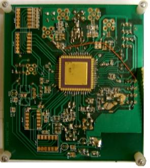
37 IV. VCO Layout Final design F. Silveira Univ. de la República, Montevideo, Uruguay EAMTA

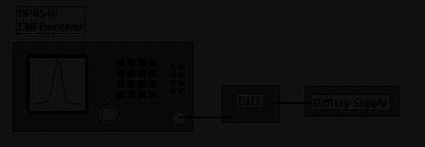
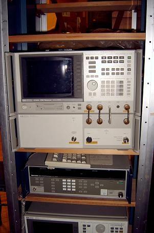
38 IV. VCO Measurements Measurement setup F. Silveira Univ. de la República, Montevideo, Uruguay EAMTA

39 IV. VCO Measurements VCO oscillation frequency versus V bias K VCO =-169MHz/V tuning range=11% K VCO =-214MHz/V tuning range=15% F. Silveira Univ. de la República, Montevideo, Uruguay EAMTA

40 IV. VCO Measurements PSD and phase IDD = 3mA, VDD=3V =-87dBc/Hz =-102dBc/Hz =-107dBc/Hz F. Silveira Univ. de la República, Montevideo, Uruguay EAMTA
41 V. Conclusions Inversion level that gives an optimum consumption for a given gain. Matlab tool which helps in the design of low power RF blocks. Feasibility of working in moderate inversion at 910MHz in 0.35µm technology. Experience in ultra low power analog design may be reused here. VCO: Moderate inversion provides a good compromise between phase noise and consumption. Layout wiring parasitics and package parasitics strongly affect performance F. Silveira Univ. de la República, Montevideo, Uruguay EAMTA
42 Thank you! F. Silveira Univ. de la República, Montevideo, Uruguay EAMTA
Quadrature GPS Receiver Front-End in 0.13μm CMOS: The QLMV cell
 1 Quadrature GPS Receiver Front-End in 0.13μm CMOS: The QLMV cell Yee-Huan Ng, Po-Chia Lai, and Jia Ruan Abstract This paper presents a GPS receiver front end design that is based on the single-stage quadrature
Fully Integrated Low Phase Noise LC VCO. Desired Characteristics of VCOs
 Fully Integrated ow Phase Noise C VCO AGENDA Comparison with other types of VCOs. Analysis of two common C VCO topologies. Design procedure for the cross-coupled C VCO. Phase noise reduction techniques.
6.776 High Speed Communication Circuits Lecture 6 MOS Transistors, Passive Components, Gain- Bandwidth Issue for Broadband Amplifiers
 6.776 High Speed Communication Circuits Lecture 6 MOS Transistors, Passive Components, Gain- Bandwidth Issue for Broadband Amplifiers Massachusetts Institute of Technology February 17, 2005 Copyright 2005
AVoltage Controlled Oscillator (VCO) was designed and
 was designed and") 1 EECE 457 VCO Design Project Jason Khuu, Erik Wu Abstract This paper details the design and simulation of a Voltage Controlled Oscillator using a 0.13µm process. The final VCO design meets all specifications.
1 EECE 457 VCO Design Project Jason Khuu, Erik Wu Abstract This paper details the design and simulation of a Voltage Controlled Oscillator using a 0.13µm process. The final VCO design meets all specifications.
Quiz2: Mixer and VCO Design
 Quiz2: Mixer and VCO Design Fei Sun and Hao Zhong 1 Question1 - Mixer Design 1.1 Design Criteria According to the specifications described in the problem, we can get the design criteria for mixer design:
A CMOS GHz UWB LNA Employing Modified Derivative Superposition Method
 Circuits and Systems, 03, 4, 33-37 http://dx.doi.org/0.436/cs.03.43044 Published Online July 03 (http://www.scirp.org/journal/cs) A 3. - 0.6 GHz UWB LNA Employing Modified Derivative Superposition Method
DESIGN OF ZIGBEE RF FRONT END IC IN 2.4 GHz ISM BAND
 DESIGN OF ZIGBEE RF FRONT END IC IN 2.4 GHz ISM BAND SUCHITAV KHADANGA RFIC TECHNOLOGIES, BANGALORE, INDIA http://www.rficdesign.com Team-RV COLLEGE Ashray V K D V Raghu Sanjith P Hemagiri Rahul Verma
Low Noise Amplifier Design
 THE UNIVERSITY OF TEXAS AT DALLAS DEPARTMENT OF ELECTRICAL ENGINEERING EERF 6330 RF Integrated Circuit Design (Spring 2016) Final Project Report on Low Noise Amplifier Design Submitted To: Dr. Kenneth
An Asymmetrical Bulk CMOS Switch for 2.4 GHz Application
 Progress In Electromagnetics Research Letters, Vol. 66, 99 104, 2017 An Asymmetrical Bulk CMOS Switch for 2.4 GHz Application Lang Chen 1, * and Ye-Bing Gan 1, 2 Abstract A novel asymmetrical single-pole
A 25-GHz Differential LC-VCO in 90-nm CMOS
 A 25-GHz Differential LC-VCO in 90-nm CMOS Törmänen, Markus; Sjöland, Henrik Published in: Proc. 2008 IEEE Asia Pacific Conference on Circuits and Systems Published: 2008-01-01 Link to publication Citation
T. Taris, H. Kraïmia, JB. Begueret, Y. Deval. Bordeaux, France. 12/15-16, 2011 Lauzanne, Switzerland
 1 MOSFET Modeling for Ultra Low-Power RF Design T. Taris, H. Kraïmia, JB. Begueret, Y. Deval Bordeaux, France 2 Context More services in Environment survey Energy management Process optimisation Aging
6.976 High Speed Communication Circuits and Systems Lecture 5 High Speed, Broadband Amplifiers
 6.976 High Speed Communication Circuits and Systems Lecture 5 High Speed, Broadband Amplifiers Michael Perrott Massachusetts Institute of Technology Copyright 2003 by Michael H. Perrott Broadband Communication
Fully-Integrated Low Phase Noise Bipolar Differential VCOs at 2.9 and 4.4 GHz
 Fully-Integrated Low Phase Noise Bipolar Differential VCOs at 2.9 and 4.4 GHz Ali M. Niknejad Robert G. Meyer Electronics Research Laboratory University of California at Berkeley Joo Leong Tham 1 Conexant
Dr.-Ing. Ulrich L. Rohde
 Dr.-Ing. Ulrich L. Rohde Noise in Oscillators with Active Inductors Presented to the Faculty 3 : Mechanical engineering, Electrical engineering and industrial engineering, Brandenburg University of Technology
A Multiobjective Optimization based Fast and Robust Design Methodology for Low Power and Low Phase Noise Current Starved VCO Gaurav Sharma 1
 IJSRD - International Journal for Scientific Research & Development Vol. 2, Issue 01, 2014 ISSN (online): 2321-0613 A Multiobjective Optimization based Fast and Robust Design Methodology for Low Power
Low-Power RF Integrated Circuit Design Techniques for Short-Range Wireless Connectivity
 Low-Power RF Integrated Circuit Design Techniques for Short-Range Wireless Connectivity Marvin Onabajo Assistant Professor Analog and Mixed-Signal Integrated Circuits (AMSIC) Research Laboratory Dept.
ISSCC 2004 / SESSION 21/ 21.1
 ISSCC 2004 / SESSION 21/ 21.1 21.1 Circular-Geometry Oscillators R. Aparicio, A. Hajimiri California Institute of Technology, Pasadena, CA Demand for faster data rates in wireline and wireless markets
ISSCC 2002 / SESSION 17 / ADVANCED RF TECHNIQUES / 17.2
 ISSCC 2002 / SESSION 17 / ADVANCED RF TECHNIQUES / 17.2 17.2 A CMOS Differential Noise-Shifting Colpitts VCO Roberto Aparicio, Ali Hajimiri California Institute of Technology, Pasadena, CA Demand for higher
RF Integrated Circuits
 Introduction and Motivation RF Integrated Circuits The recent explosion in the radio frequency (RF) and wireless market has caught the semiconductor industry by surprise. The increasing demand for affordable
CHAPTER 3 CMOS LOW NOISE AMPLIFIERS
 46 CHAPTER 3 CMOS LOW NOISE AMPLIFIERS 3.1 INTRODUCTION The Low Noise Amplifier (LNA) plays an important role in the receiver design. LNA serves as the first block in the RF receiver. It is a critical
SP 22.3: A 12mW Wide Dynamic Range CMOS Front-End for a Portable GPS Receiver
 SP 22.3: A 12mW Wide Dynamic Range CMOS Front-End for a Portable GPS Receiver Arvin R. Shahani, Derek K. Shaeffer, Thomas H. Lee Stanford University, Stanford, CA At submicron channel lengths, CMOS is
95GHz Receiver with Fundamental Frequency VCO and Static Frequency Divider in 65nm Digital CMOS
 95GHz Receiver with Fundamental Frequency VCO and Static Frequency Divider in 65nm Digital CMOS Ekaterina Laskin, Mehdi Khanpour, Ricardo Aroca, Keith W. Tang, Patrice Garcia 1, Sorin P. Voinigescu University
Radivoje Đurić, 2015, Analogna Integrisana Kola 1
 Low power OTA 1 Two-Stage, Miller Op Amp Operating in Weak Inversion Low frequency response: gm1 gm6 Av 0 g g g g A v 0 ds2 ds4 ds6 ds7 I D m, ds D nvt g g I n GB and SR: GB 1 1 n 1 2 4 6 6 7 g 2 2 m1
ETI , Good luck! Written Exam Integrated Radio Electronics. Lund University Dept. of Electroscience
 und University Dept. of Electroscience EI170 Written Exam Integrated adio Electronics 2010-03-10, 08.00-13.00 he exam consists of 5 problems which can give a maximum of 6 points each. he total maximum
Streamlined Design of SiGe Based Power Amplifiers
 ROMANIAN JOURNAL OF INFORMATION SCIENCE AND TECHNOLOGY Volume 13, Number 1, 2010, 22 32 Streamlined Design of SiGe Based Power Amplifiers Mladen BOŽANIĆ1, Saurabh SINHA 1, Alexandru MÜLLER2 1 Department
Long Range Passive RF-ID Tag With UWB Transmitter
 Long Range Passive RF-ID Tag With UWB Transmitter Seunghyun Lee Seunghyun Oh Yonghyun Shim seansl@umich.edu austeban@umich.edu yhshim@umich.edu About RF-ID Tag What is a RF-ID Tag? An object for the identification
EVALUATION KIT AVAILABLE 10MHz to 1050MHz Integrated RF Oscillator with Buffered Outputs. Typical Operating Circuit. 10nH 1000pF MAX2620 BIAS SUPPLY
 19-1248; Rev 1; 5/98 EVALUATION KIT AVAILABLE 10MHz to 1050MHz Integrated General Description The combines a low-noise oscillator with two output buffers in a low-cost, plastic surface-mount, ultra-small
Design of a Low Power 5GHz CMOS Radio Frequency Low Noise Amplifier Rakshith Venkatesh
 Design of a Low Power 5GHz CMOS Radio Frequency Low Noise Amplifier Rakshith Venkatesh Abstract A 5GHz low power consumption LNA has been designed here for the receiver front end using 90nm CMOS technology.
Design of a Reusable Rail-to-Rail Operational Amplifier
 Design of a Reusable RailtoRail Operational Amplifier Pablo Aguirre, Fernando Silveira Instituto de Ingeniería Eléctrica Universidad de la República Montevideo, Uruguay. paguirre@fing.edu.uy Abstract This
Lecture 160 Examples of CDR Circuits in CMOS (09/04/03) Page 160-1
 Page 160-1") Lecture 160 Examples of CDR Circuits in CMOS (09/04/03) Page 160-1 LECTURE 160 CDR EXAMPLES INTRODUCTION Objective The objective of this presentation is: 1.) Show two examples of clock and data recovery
Lecture 160 Examples of CDR Circuits in CMOS (09/04/03) Page 160-1 LECTURE 160 CDR EXAMPLES INTRODUCTION Objective The objective of this presentation is: 1.) Show two examples of clock and data recovery
PART MAX2605EUT-T MAX2606EUT-T MAX2607EUT-T MAX2608EUT-T MAX2609EUT-T TOP VIEW IND GND. Maxim Integrated Products 1
 19-1673; Rev 0a; 4/02 EVALUATION KIT MANUAL AVAILABLE 45MHz to 650MHz, Integrated IF General Description The are compact, high-performance intermediate-frequency (IF) voltage-controlled oscillators (VCOs)
A 20GHz Class-C VCO Using Noise Sensitivity Mitigation Technique
 Matsuzawa Lab. Matsuzawa & Okada Lab. Tokyo Institute of Technology A 20GHz Class-C VCO Using Noise Sensitivity Mitigation Technique Kento Kimura, Kenichi Okada and Akira Matsuzawa (WE2C-2) Matsuzawa &
A Low Phase Noise LC VCO for 6GHz
 A Low Phase Noise LC VCO for 6GHz Mostafa Yargholi 1, Abbas Nasri 2 Department of Electrical Engineering, University of Zanjan, Zanjan, Iran 1 yargholi@znu.ac.ir, 2 abbas.nasri@znu.ac.ir, Abstract: This
A 10-GHz CMOS LC VCO with Wide Tuning Range Using Capacitive Degeneration
 JOURNAL OF SEMICONDUCTOR TECHNOLOGY AND SCIENCE, VOL.6, NO.4, DECEMBER, 2006 281 A 10-GHz CMOS LC VCO with Wide Tuning Range Using Capacitive Degeneration Tae-Geun Yu, Seong-Ik Cho, and Hang-Geun Jeong
Highly linear common-gate mixer employing intrinsic second and third order distortion cancellation
 Highly linear common-gate mixer employing intrinsic second and third order distortion cancellation Mahdi Parvizi a), and Abdolreza Nabavi b) Microelectronics Laboratory, Tarbiat Modares University, Tehran
A Novel Design of Low Voltage,Wilson Current Mirror based Wideband Operational Transconductance Amplifier
 A Novel Design of Low Voltage,Wilson Current Mirror based Wideband Operational Transconductance Amplifier Kehul A. Shah 1, N.M.Devashrayee 2 1(Associative Prof., Department of Electronics and Communication,
A HIGH FIGURE-OF-MERIT LOW PHASE NOISE 15-GHz CMOS VCO
 82 Journal of Marine Science and Technology, Vol. 21, No. 1, pp. 82-86 (213) DOI: 1.6119/JMST-11-123-1 A HIGH FIGURE-OF-MERIT LOW PHASE NOISE 15-GHz MOS VO Yao-hian Lin, Mei-Ling Yeh, and hung-heng hang
An Optimal Design of Ring Oscillator and Differential LC using 45 nm CMOS Technology
 IJIRST International Journal for Innovative Research in Science & Technology Volume 2 Issue 10 March 2016 ISSN (online): 2349-6010 An Optimal Design of Ring Oscillator and Differential LC using 45 nm CMOS
i. At the start-up of oscillation there is an excess negative resistance (-R)
") OSCILLATORS Andrew Dearn * Introduction The designers of monolithic or integrated oscillators usually have the available process dictated to them by overall system requirements such as frequency of operation
OSCILLATORS Andrew Dearn * Introduction The designers of monolithic or integrated oscillators usually have the available process dictated to them by overall system requirements such as frequency of operation
WITH advancements in submicrometer CMOS technology,
 IEEE TRANSACTIONS ON MICROWAVE THEORY AND TECHNIQUES, VOL. 53, NO. 3, MARCH 2005 881 A Complementary Colpitts Oscillator in CMOS Technology Choong-Yul Cha, Member, IEEE, and Sang-Gug Lee, Member, IEEE
A 60GHz CMOS Power Amplifier Using Varactor Cross-Coupling Neutralization with Adaptive Bias
 A 6GHz CMOS Power Amplifier Using Varactor Cross-Coupling Neutralization with Adaptive Bias Ryo Minami,Kota Matsushita, Hiroki Asada, Kenichi Okada,and Akira Tokyo Institute of Technology, Japan Outline
Low-Noise Amplifiers
 007/Oct 4, 31 1 General Considerations Noise Figure Low-Noise Amplifiers Table 6.1 Typical LNA characteristics in heterodyne systems. NF IIP 3 db 10 dbm Gain 15 db Input and Output Impedance 50 Ω Input
Design and Simulation of Voltage-Mode and Current-Mode Class-D Power Amplifiers for 2.4 GHz Applications
 Design and Simulation of Voltage-Mode and Current-Mode Class-D Power Amplifiers for 2.4 GHz Applications Armindo António Barão da Silva Pontes Abstract This paper presents the design and simulations of
10MHz to 1050MHz Integrated RF Oscillator with Buffered Outputs
 9-24; Rev 2; 2/02 EVALUATION KIT AVAILABLE 0MHz to 050MHz Integrated General Description The combines a low-noise oscillator with two output buffers in a low-cost, plastic surface-mount, ultra-small µmax
MP 4.3 Monolithic CMOS Distributed Amplifier and Oscillator
 MP 4.3 Monolithic CMOS Distributed Amplifier and Oscillator Bendik Kleveland, Carlos H. Diaz 1 *, Dieter Vook 1, Liam Madden 2, Thomas H. Lee, S. Simon Wong Stanford University, Stanford, CA 1 Hewlett-Packard
1-13GHz Wideband LNA utilizing a Transformer as a Compact Inter-stage Network in 65nm CMOS
 -3GHz Wideband LNA utilizing a Transformer as a Compact Inter-stage Network in 65nm CMOS Hyohyun Nam and Jung-Dong Park a Division of Electronics and Electrical Engineering, Dongguk University, Seoul E-mail
Layout Design of LC VCO with Current Mirror Using 0.18 µm Technology
 Wireless Engineering and Technology, 2011, 2, 102106 doi:10.4236/wet.2011.22014 Published Online April 2011 (http://www.scirp.org/journal/wet) 99 Layout Design of LC VCO with Current Mirror Using 0.18
A 2.4 GHz to 3.86 GHz digitally controlled oscillator with 18.5 khz frequency resolution using single PMOS varactor
 LETTER IEICE Electronics Express, Vol.9, No.24, 1842 1848 A 2.4 GHz to 3.86 GHz digitally controlled oscillator with 18.5 khz frequency resolution using single PMOS varactor Yangyang Niu, Wei Li a), Ning
A 5.5 GHz Voltage Control Oscillator (VCO) with a Differential Tunable Active and Passive Inductor
 with a Differential Tunable Active and Passive Inductor") A. GHz Voltage Control Oscillator (VCO) with a Differential Tunable Active and Passive Inductor Najmeh Cheraghi Shirazi, Ebrahim Abiri, and Roozbeh Hamzehyan, ember, IACSIT Abstract By using a differential
A. GHz Voltage Control Oscillator (VCO) with a Differential Tunable Active and Passive Inductor Najmeh Cheraghi Shirazi, Ebrahim Abiri, and Roozbeh Hamzehyan, ember, IACSIT Abstract By using a differential
1P6M 0.18-µm Low Power CMOS Ring Oscillator for Radio Frequency Applications
 1P6M 0.18-µm Low Power CMOS Ring Oscillator for Radio Frequency Applications Ashish Raman and R. K. Sarin Abstract The monograph analysis a low power voltage controlled ring oscillator, implement using
THE BASIC BUILDING BLOCKS OF 1.8 GHZ PLL
 THE BASIC BUILDING BLOCKS OF 1.8 GHZ PLL IN CMOS TECHNOLOGY L. Majer, M. Tomáška,V. Stopjaková, V. Nagy, and P. Malošek Department of Microelectronics, Slovak Technical University, Ilkovičova 3, Bratislava,
FD-SOI FOR RF IC DESIGN. SITRI LETI Workshop Mercier Eric 08 september 2016
 FD-SOI FOR RF IC DESIGN SITRI LETI Workshop Mercier Eric 08 september 2016 UTBB 28 nm FD-SOI : RF DIRECT BENEFITS (1/2) 3 back-end options available Routing possible on the AluCap level no restriction
20 GHz Low Power QVCO and De-skew Techniques in 0.13µm Digital CMOS. Masum Hossain & Tony Chan Carusone University of Toronto
 20 GHz Low Power QVCO and De-skew Techniques in 0.13µm Digital CMOS Masum Hossain & Tony Chan Carusone University of Toronto masum@eecg.utoronto.ca Motivation Data Rx3 Rx2 D-FF D-FF Rx1 D-FF Clock Clock
A 5GHz, 32mW CMOS Frequency Synthesizer with an Injection Locked Frequency Divider. Hamid Rategh, Hirad Samavati, Thomas Lee
 A 5GHz, 32mW CMOS Frequency Synthesizer with an Injection Locked Frequency Divider Hamid Rategh, Hirad Samavati, Thomas Lee OUTLINE motivation introduction synthesizer architecture synthesizer building
An 8mA, 3.8dB NF, 40dB Gain CMOS Front-End for GPS Applications
 An 8mA, 3.8dB NF, 40dB Gain CMOS Front-End for GPS Applications F. Svelto S. Deantoni, G. Montagna R. Castello Dipartimento di Ingegneria Studio di Microelettronica Dipartimento di Elettronica Università
Hot Topics and Cool Ideas in Scaled CMOS Analog Design
 Engineering Insights 2006 Hot Topics and Cool Ideas in Scaled CMOS Analog Design C. Patrick Yue ECE, UCSB October 27, 2006 Slide 1 Our Research Focus High-speed analog and RF circuits Device modeling,
An Inductor-Based 52-GHz 0.18 µm SiGe HBT Cascode LNA with 22 db Gain
 An Inductor-Based 52-GHz 0.18 µm SiGe HBT Cascode LNA with 22 db Gain Michael Gordon, Sorin P. Voinigescu University of Toronto Toronto, Ontario, Canada ESSCIRC 2004, Leuven, Belgium Outline Motivation
Project #3 for Electronic Circuit II
 Project #3 for Electronic Circuit II Prof. Woo-Young Choi TA: Tongsung Kim, Minkyu Kim June 1, 2015 - Deadline : 6:00 pm on June 22, 2015. Penalties for late hand-in. - Team Students are expected to form
Fully integrated CMOS transmitter design considerations
 Semiconductor Technology Fully integrated CMOS transmitter design considerations Traditionally, multiple IC chips are needed to build transmitters (Tx) used in wireless communications. The difficulty with
Christopher J. Barnwell ECE Department U. N. Carolina at Charlotte Charlotte, NC, 28223, USA
 Copyright 2008 IEEE. Published in IEEE SoutheastCon 2008, April 3-6, 2008, Huntsville, A. Personal use of this material is permitted. However, permission to reprint/republish this material for advertising
DESIGN OF 2.4 GHZ LOW POWER CMOS TRANSMITTER FRONT END
 Volume 117 No. 16 2017, 685-694 ISSN: 1311-8080 (printed version); ISSN: 1314-3395 (on-line version) url: http://www.ijpam.eu ijpam.eu DESIGN OF 2.4 GHZ LOW POWER CMOS TRANSMITTER FRONT END 1 S.Manjula,
A 3 5 GHz CMOS High Linearity Ultra Wideband Low Noise Amplifier in 0.18µ CMOS
 Proceedings of the 5th WSEAS Int. Conf. on CIRCUITS, SYSTEMS, ELECTRONICS, CONTROL & SIGNAL PROCESSING, Dallas, USA, November -, 6 5 A 5 GHz CMOS High Linearity Ultra Wideband Low Noise Amplifier in.8µ
Case Study: Osc2 Design of a C-Band VCO
 MICROWAVE AND RF DESIGN Case Study: Osc2 Design of a C-Band VCO Presented by Michael Steer Reading: Chapter 20, 20.5,6 Index: CS_Osc2 Based on material in Microwave and RF Design: A Systems Approach, 2
CMOS analog amplier design problem: choose transistor dimensions, bias currents, component values critical part of mixed-mode (digital-analog) ICs for
 ICs for") Op-amp Design and Optimization via CMOS Programming Geometric Mar Hershenson, Stephen Boyd, Thomas Lee Engineering Department Electrical University Stanford UCSB 10/24/97 CMOS analog amplier design problem:
Op-amp Design and Optimization via CMOS Programming Geometric Mar Hershenson, Stephen Boyd, Thomas Lee Engineering Department Electrical University Stanford UCSB 10/24/97 CMOS analog amplier design problem:
Review of ASITIC (Analysis and Simulation of Inductors and Transformers for Integrated Circuits) Tool to Design Inductor on Chip
 Tool to Design Inductor on Chip") www.ijcsi.org 196 Review of ASITIC (Analysis and Simulation of Inductors and Transformers for Integrated Circuits) Tool to Design Inductor on Chip M. Zamin Ali Khan 1, Hussain Saleem 2 and Shiraz Afzal
www.ijcsi.org 196 Review of ASITIC (Analysis and Simulation of Inductors and Transformers for Integrated Circuits) Tool to Design Inductor on Chip M. Zamin Ali Khan 1, Hussain Saleem 2 and Shiraz Afzal
DESIGN OF 3 TO 5 GHz CMOS LOW NOISE AMPLIFIER FOR ULTRA-WIDEBAND (UWB) SYSTEM
 SYSTEM") Progress In Electromagnetics Research C, Vol. 9, 25 34, 2009 DESIGN OF 3 TO 5 GHz CMOS LOW NOISE AMPLIFIER FOR ULTRA-WIDEBAND (UWB) SYSTEM S.-K. Wong and F. Kung Faculty of Engineering Multimedia University
Progress In Electromagnetics Research C, Vol. 9, 25 34, 2009 DESIGN OF 3 TO 5 GHz CMOS LOW NOISE AMPLIFIER FOR ULTRA-WIDEBAND (UWB) SYSTEM S.-K. Wong and F. Kung Faculty of Engineering Multimedia University
Design of a Low Noise Amplifier using 0.18µm CMOS technology
 The International Journal Of Engineering And Science (IJES) Volume 4 Issue 6 Pages PP.11-16 June - 2015 ISSN (e): 2319 1813 ISSN (p): 2319 1805 Design of a Low Noise Amplifier using 0.18µm CMOS technology
A GSM Band Low-Power LNA 1. LNA Schematic
 A GSM Band Low-Power LNA 1. LNA Schematic Fig1.1 Schematic of the Designed LNA 2. Design Summary Specification Required Simulation Results Peak S21 (Gain) > 10dB >11 db 3dB Bandwidth > 200MHz (
POSTECH Activities on CMOS based Linear Power Amplifiers
 1 POSTECH Activities on CMOS based Linear Power Amplifiers Jan. 16. 2006 Bumman Kim, & Jongchan Kang MMIC Laboratory Department of EE, POSTECH Presentation Outline 2 Motivation Basic Design Approach CMOS
Depletion-mode operation ( 공핍형 ): Using an input gate voltage to effectively decrease the channel size of an FET
: Using an input gate voltage to effectively decrease the channel size of an FET") Ch. 13 MOSFET Metal-Oxide-Semiconductor Field-Effect Transistor : I D D-mode E-mode V g The gate oxide is made of dielectric SiO 2 with e = 3.9 Depletion-mode operation ( 공핍형 ): Using an input gate voltage
Ch. 13 MOSFET Metal-Oxide-Semiconductor Field-Effect Transistor : I D D-mode E-mode V g The gate oxide is made of dielectric SiO 2 with e = 3.9 Depletion-mode operation ( 공핍형 ): Using an input gate voltage
Class E broadband amplifier with C-LC shunt network
 San Diego, CA Jan 09 CLASS E RF/MICROWAVE POWER AMPLIFIERS Class E broadband amplifier with C-LC shunt network Basic theory, simulation and prototype A. Mediano, K. Narendra 2, C. Prakash 2, I3A, University
Quadrature Generation Techniques in CMOS Relaxation Oscillators. S. Aniruddhan Indian Institute of Technology Madras Chennai, India
 Quadrature Generation Techniques in CMOS Relaxation Oscillators S. Aniruddhan Indian Institute of Technology Madras Chennai, India Outline Introduction & Motivation Quadrature Relaxation Oscillators (QRXO)
A Pulse-Based CMOS Ultra-Wideband Transmitter for WPANs
 A Pulse-Based CMOS Ultra-Wideband Transmitter for WPANs Murat Demirkan* Solid-State Circuits Research Laboratory University of California, Davis *Now with Agilent Technologies, Santa Clara, CA 03/20/2008
Low Phase Noise C band HBT VCO. GaAs Monolithic Microwave IC
 Frequency (GHz) GaAs Monolithic Microwave IC Description The is a low phase noise C band HBT voltage controlled oscillator that integrates negative resistor, varactors and buffer amplifiers. It provides
Sensors & Transducers Published by IFSA Publishing, S. L.,
 Sensors & Transducers Published by IFSA Publishing, S. L., 208 http://www.sensorsportal.com Fully Differential Operation Amplifier Using Self Cascode MOSFET Structure for High Slew Rate Applications Kalpraj
CHAPTER 4 ULTRA WIDE BAND LOW NOISE AMPLIFIER DESIGN
 93 CHAPTER 4 ULTRA WIDE BAND LOW NOISE AMPLIFIER DESIGN 4.1 INTRODUCTION Ultra Wide Band (UWB) system is capable of transmitting data over a wide spectrum of frequency bands with low power and high data
CMOS Dual Band Receiver GSM 900-Mhz / DSS-GSM1800-GHz
 CMOS Dual Band Receiver GSM 900-Mhz / DSS-GSM1800-GHz By : Dhruvang Darji 46610334 Transistor integrated Circuit A Dual-Band Receiver implemented with a weaver architecture with two frequency stages operating
6.976 High Speed Communication Circuits and Systems Lecture 11 Voltage Controlled Oscillators
 6.976 High Speed Communication Circuits and Systems Lecture 11 Voltage Controlled Oscillators Michael Perrott Massachusetts Institute of Technology Copyright 2003 by Michael H. Perrott VCO Design for Wireless
Chapter 2 CMOS at Millimeter Wave Frequencies
 Chapter 2 CMOS at Millimeter Wave Frequencies In the past, mm-wave integrated circuits were always designed in high-performance RF technologies due to the limited performance of the standard CMOS transistors
A 2.4GHz Cascode CMOS Low Noise Amplifier
 A 2.4GHz Cascode CMOS Low Noise Amplifier Gustavo Campos Martins, Fernando Rangel de Sousa Federal University of Santa Catarina (UFSC) Integrated Circuits Laboratory (LCI) August 31, 2012 G. C. Martins,
A 2.6GHz/5.2GHz CMOS Voltage-Controlled Oscillator*
 WP 23.6 A 2.6GHz/5.2GHz CMOS Voltage-Controlled Oscillator* Christopher Lam, Behzad Razavi University of California, Los Angeles, CA New wireless local area network (WLAN) standards have recently emerged
ALow Voltage Wide-Input-Range Bulk-Input CMOS OTA
 Analog Integrated Circuits and Signal Processing, 43, 127 136, 2005 c 2005 Springer Science + Business Media, Inc. Manufactured in The Netherlands. ALow Voltage Wide-Input-Range Bulk-Input CMOS OTA IVAN
Designing a 960 MHz CMOS LNA and Mixer using ADS. EE 5390 RFIC Design Michelle Montoya Alfredo Perez. April 15, 2004
 Designing a 960 MHz CMOS LNA and Mixer using ADS EE 5390 RFIC Design Michelle Montoya Alfredo Perez April 15, 2004 The University of Texas at El Paso Dr Tim S. Yao ABSTRACT Two circuits satisfying the
Solid State Devices & Circuits. 18. Advanced Techniques
 ECE 442 Solid State Devices & Circuits 18. Advanced Techniques Jose E. Schutt-Aine Electrical l&c Computer Engineering i University of Illinois jschutt@emlab.uiuc.edu 1 Darlington Configuration - Popular
SiNANO-NEREID Workshop:
 SiNANO-NEREID Workshop: Towards a new NanoElectronics Roadmap for Europe Leuven, September 11 th, 2017 WP3/Task 3.2 Connectivity RF and mmw Design Outline Connectivity, what connectivity? High data rates
RF Noise Simulation for Submicron MOSFET s Based on Hydrodynamic Model
 RF Noise Simulation for Submicron MOSFET s Based on Hydrodynamic Model Jung-Suk Goo, Chang-Hoon Choi, Eiji Morifuji, Hisayo Sasaki Momose, Zhiping Yu, Hiroshi Iwai, Thomas H. Lee, and Robert W. Dutton,
Keywords Divide by-4, Direct injection, Injection locked frequency divider (ILFD), Low voltage, Locking range.
, Low voltage, Locking range.") Volume 6, Issue 4, April 2016 ISSN: 2277 128X International Journal of Advanced Research in Computer Science and Software Engineering Research Paper Available online at: www.ijarcsse.com Design of CMOS
Volume 6, Issue 4, April 2016 ISSN: 2277 128X International Journal of Advanced Research in Computer Science and Software Engineering Research Paper Available online at: www.ijarcsse.com Design of CMOS
A LOW POWER CMOS TRANSCEIVER DESIGN FOR MEDICAL IMPANT COMMUNICATION SERVICE
 A LOW POWER CMOS TRANSCEIVER DESIGN FOR MEDICAL IMPANT COMMUNICATION SERVICE Huseyin S Savci, Pin Ying, Zheng Wang and Prof. Numan S. Dogan North Carolina A&T State University An ultra low power CMOS transceiver
Nonlinear Macromodeling of Amplifiers and Applications to Filter Design.
 ECEN 622(ESS) Nonlinear Macromodeling of Amplifiers and Applications to Filter Design. By Edgar Sanchez-Sinencio Thanks to Heng Zhang for part of the material OP AMP MACROMODELS Systems containing a significant
Analysis and Design of a Family of Low-Power Class AB Operational Amplifiers
 Analysis and Design of a Family of Low-Power Class AB Operational Amplifiers Fernando Silveira Instituto de Ing. Ele'ctrica, Universidad de la Republica, Montevideo, Uruguay. silveira @ iie. edu. uy Denis
A 2.4-GHz 24-dBm SOI CMOS Power Amplifier with Fully Integrated Output Balun and Switched Capacitors for Load Line Adaptation
 A 2.4-GHz 24-dBm SOI CMOS Power Amplifier with Fully Integrated Output Balun and Switched Capacitors for Load Line Adaptation Francesco Carrara 1, Calogero D. Presti 2,1, Fausto Pappalardo 1, and Giuseppe
A 3 8 GHz Broadband Low Power Mixer
 PIERS ONLINE, VOL. 4, NO. 3, 8 361 A 3 8 GHz Broadband Low Power Mixer Chih-Hau Chen and Christina F. Jou Institute of Communication Engineering, National Chiao Tung University, Hsinchu, Taiwan Abstract
DEEP-SUBMICROMETER CMOS processes are attractive
 IEEE TRANSACTIONS ON MICROWAVE THEORY AND TECHNIQUES, VOL. 59, NO. 7, JULY 2011 1811 Gm-Boosted Differential Drain-to-Source Feedback Colpitts CMOS VCO Jong-Phil Hong and Sang-Gug Lee, Member, IEEE Abstract
Challenges in Designing CMOS Wireless System-on-a-chip
 Challenges in Designing CMOS Wireless System-on-a-chip David Su Atheros Communications Santa Clara, California IEEE Fort Collins, March 2008 Introduction Outline Analog/RF: CMOS Transceiver Building Blocks
Chapter 4 Single-stage MOS amplifiers
 Chapter 4 Single-stage MOS amplifiers ELEC-H402/CH4: Single-stage MOS amplifiers 1 Single-stage MOS amplifiers NMOS as an amplifier: example of common-source circuit NMOS amplifier example Introduction
Low Power Low Phase Noise CMOS LC VCO A Review
 Low Power Low Phase Noise CMOS LC VCO A Review M.A.Nandanwar Research Scholar B.D.College of Engineering.Sewagram M.A.Gaikwad P.G.Department of Electronics Engineering B.D.C.O.E.Sewagram D.Dandekar P.G.Department
Noise Reduction in Transistor Oscillators: Part 3 Noise Shifting Techniques. cross-coupled. over other topolo-
 From July 2005 High Frequency Electronics Copyright 2005 Summit Technical Media Noise Reduction in Transistor Oscillators: Part 3 Noise Shifting Techniques By Andrei Grebennikov M/A-COM Eurotec Figure
Design of 2.4 GHz Oscillators In CMOS Technology
 Design of 2.4 GHz Oscillators In CMOS Technology Mr. Pravin Bodade Department of electronics engineering Priyadarshini College of engineering Nagpur, India prbodade@gmail.com Ms. Divya Meshram Department
A Wide Tuning Range Gm-C Continuous-Time Analog Filter
 A Wide Tuning Range Gm-C Continuous-Time Analog Filter Prashanth Kannepally Dept. of Electronics and Communication Engineering SNIST Hyderabad, India 685project6801@gmail.com Abstract A Wide Tuning Range
Measurement and Modeling of CMOS Devices in Short Millimeter Wave. Minoru Fujishima
 Measurement and Modeling of CMOS Devices in Short Millimeter Wave Minoru Fujishima Our position We are circuit designers. Our final target is not device modeling, but chip demonstration. Provided device