Since
|
|
|
- Ambrose Warner
- 5 years ago
- Views:
Transcription


1 Since


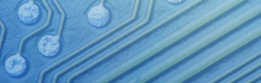
2 Advanced Laserr Technology at KORTherm Science S Since founded in 1999 we put our endeavor into building a specialized business, focusing on the application of lasers and NANO/MEMS with high hest quality. quality With the laser micro-machining system and LD laser system at our research center, we have been dedicating ourselves to develop a total laser solution such as solar cell scribing, hole drilliing, laser patterning, welding, and grooving tools. As one of the leading laser system integrators of ph hotovoltaic industry, we promise to provide the best products worldwide with respect to value, performa ance, range, and efficiency. Thanks to ceaseless encouragement from our cusstomers and partners over the world, we have greatly achieved so much success to place KORTherm m among the best companies in the laser micromachining sector. By responding to our customer's needs more proactively with continuous efforts in R&D and management innovation, we will keep growing to be the world's leading company in the laser micromachining g sector. Sincerely, Ju-Sam Byeon, CEO 2


3 Contribution to green industry through our technology and experience we have accumulated. Leaping to the best enterprise in order to make better world. Creation of value through technical t renovation. Solar cell c Pattern ning Laser Cutting FPD Medical Device ELA Laser Drilling Laser Patterning Marking Scribing 3


4 HISTORY µ-solar, a solar cell scribing tool, has been launched Currently developing a laser water-jet production technology. Headquarter moved to Bupyeong, Incheon. Uniquely deveoped proprietary software Head office moved to Seoul. 10th anniversary Selected as an INNO-BIZ Z company in response to innovation technology technology. esearch Set up the center of the re institute for laser application technology. ng Developed laser patternin technology for large sized d glass Developed KOS series: laser micro machining system Founded at Saha-Gu, Busan,Korea.


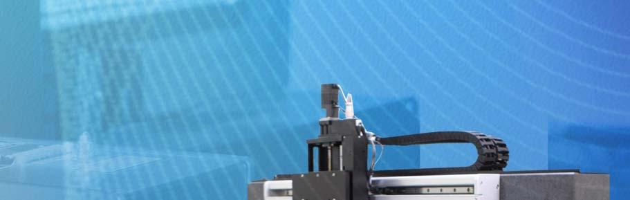
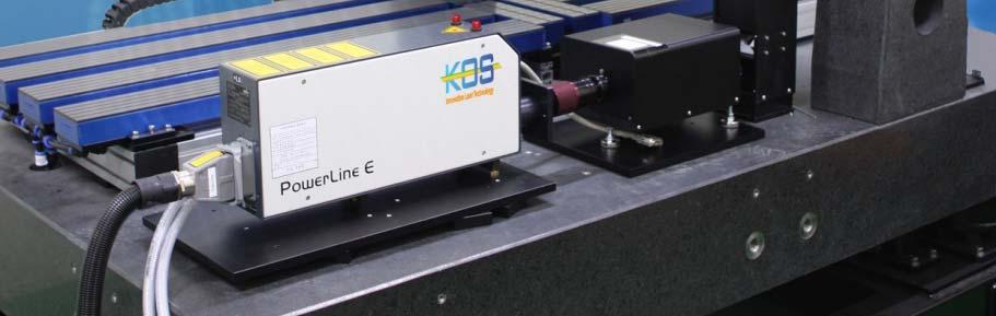
5 PRODCUCT LINE Advanced Laser Technology KOS LP Series The KOS LP Series are large flat panel multipurpose laser cutting systems built from state of the art technology. These systems are equipped with a high power energy-efficient DPSS laser and advanced linear motion control platform. μ-combo µ-combo is a compact and versatile laser micromachining tool with multiple wavelengths applying to drilling, scribing and cutting operations, specifically designed for the development of high- precision micromachining applications. KOS Ablator Series The KOS Ablator Series are designed to cut the wafer with a high powered and energy efficient DPSS laser. Compared to other laser cutting machine, the KOS Ablator offers a lighter weight design and the fastest cutting speed. μ-solar μ-solar provides ideal solutions for photovoltaic cell production with a high-precision laser technology. KORTherm Science offers a range of powers and frequencies of micromachining systems for scribing of accurate and small width of line patterning (30~50 um). With the appropriate choice of lasers, this system provides users with powerful solution for Si wafer and thin-film solar cell production. Laser Diode System We produce Laser Diode System (LDS) with UV, visible, and IR wavelength. Especially, current and temperature controller can offer laser power up to 10W and wavelength with promising high current and temperature stability. 5


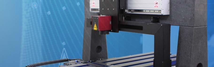
6 KOS LP Series Micromachining Tool for Large Area Laser processing of display devices The KOS LP is an ideal laser micromachining system to pattern various kinds of materials. It has been specially developed by KORTherm in order to meet the demanding challenges of large area tools for in-line: LCD, PDP, OLED, and a solar cell line. The KOS LP has reduced running costs with a high efficiency. Coping with the various requirements, we are always ready to follow up the customer s needs whatever it takes. Less than 20um band scribing Raster scanning to cover large areas with micro-structures Automatically loading/unloading This tool comes with robot loading and manual sheet loading. High speed processing more than 1200mm/s Alternative tool replacing chemica al process KOS LP Series can scribe glass panel and thin film with a high speed. Auto alignment system High resolution alignment optics module corrects the glass panel position. KOS LP Series use angular offset spatially. Customized beam relay and homogenization optics Air-floating chuck system When patterning the large area with KOS LP Series, thin film (metal, organic, TCO etc.) on the substrate can be processed through the air floating chuck and the air base clamp. 6


7 Large substrate capability Microstructuring and selective ablation Micro-drilling and engraving PDP/LCD panel cutting Environmentally friendly process High accuracy Advanced optical technique transports the high quality laser beam incident on the solar cell substrate. Work piece Laser Wavelength Cooling Line Width Stage Resolution Processing Speed Power Consumption Up to 10G sized panel DPSS / Excimer 355, 532, 1064nm Air / Water 5~100μm Conveyor / Air floating 0.5 um More than 1200mm/s 6.0 kva Processed Material Dimension Weight ITO, metal, Si, ceramic, GaAs etc mm x 4000 mm x 2000mm (5G) 4800 kg (5G) 7


 can be processed.")

8 µ-combo Dual Laser Microprocessing System Dual laser stand alone system for R&D µ-combo is a compact and versatile laser micromachining tool with multiple wavelengths applying to drilling, scribing and cutting operations. Specifically designed for the development of high-precisionh ii micromachining i applications, it can be implemented in R&D environment as a stand-alone system. The µ-combo machining tool covers a range of micro sized materials on glass including metal, Si, polymer etc. High quality processing Proven laser technologies guarantee high precision processing. µ-combo has high speed scribing more than 1200mm/s. Ultra thin substrates t (less than 5um) can be processed. Dual laser tool Multi leveled layers can be processed with both diode pumped laser and excimer laser µ-combo fits with both a solid-state laser and a high pulsed repetition rate of excimer laser. Polymer masters for replication in metal. Auto alignment with spatial and angular offset A dual vision system makes easier to align offset. Software An easy-to-use Windows user interface enables rapid and powerful control of the operation of the µ-combo. 8


 Weight 300mm (12 inches) DPSS, Excimer")

9 Dual laser systems with various applications 3D manufacturing Laser hole drilling and engravingg Solar cell scribing Wafer / PCB/ metal cutting Single step process (eliminating complex lithography) ITO layer on polyester substrate Work piece Laser Wavelength Cooling Line Width Resolution Processing Speed Power Consumption Cutting Thickness Dimension(mm) Weight 300mm (12 inches) DPSS, Excimer 193, 248, 266, 355, 532, 1064 nm Air / Water 5~100um 0.5 um More than 1200 mm/sec 6.0 kva ~50um 1800 x 1700 x 2000(mm) 1800 kg 9


10 KOS Ablator Series Laser Ablating System High-precision and powerful laser method for wafer-cutting! KOS Ablator Series provide ideal solutions for ultra-thin wafers with a high-precision laser technology created by KORTherm Science. With a dual vision system, KOS Ablator Series recognize the state-of-the-art alignment together with a high performance stage. The visualized software designed to control all units makes it possible to cut curvilinear shape as well as process 3D structures including trenches in controlled depth. The KOS Ablator also gives better performance in damages for patterned materials on glass than Blade dicing. TheKOSAblator is a laser-based micromachining tool specifically designed for the rapid removal of thin layers of material from wafer in a chemical-free and single-state process. Improved dicing speed The KOS Ablator Series recognize high speed cutting for 200µm thickness at a speed than 500mm/s Improved yield As the wafer is cut internally by avoiding any damage to the wafer surface, the KOS Ablator minimizes chipping/cracking on the bottom surface of the wafer and improves flexural strength and tact in the die bonding process as well as contributes to better yield. High reliability When irradiating the reverse side with a lase er, the wafer can be conveyed by support handing. Low cost of ownership No use of blades reduces the running costs, and labor is not required for blade replacement and quality control of blade wear and tear. 10


11 High precision i and powerful meth od for cutting and dicing i Plastic/Fabric cutting Metal cutting PCB cutting Glass cutting Ceramic cutting Flex circuit machining Wafer Size Laser Wavelength Cooling Line Width Resolution Processing Speed Power Consumption Assist Gas Pressure Cutting Thickness Dimension Weight 300mm (12 inches) DPSS / Fiber laser 266, 355, 532, 1064nm Air / water Less than 50um 0.5 um More than 500 mm/sec 6.0 kva < 0.7 Mpa Up to 300μm 1800 mm x 1600 mm x 1900mm 1800 kg 11
.")

12 µ-solar Laser Solar Cell Scribing Tool Laser scribing tool for silicon based solar cell µ-solar provides us with ideal solutions for photovoltaic cell production with a high-precision laser technology. KO ORTherm Science offers a range of powers and frequencies of micromachining systems for scribing of accurate and small width of line patterning (30 ~50 um). With the appropriate choice of lasers, this system provides users with powerful solutions for Si wafer and thin-film solar cell production. The visualized software designed to co ontrol all units makes it possible to process line shape as well as edge isolation. µ-solar also provides us with the low damage and low cost during wafer/thin film patterning process compared with lithography /etching process. High quality processing Solar cell scribing thin layers High speed scribing up to 800mm/s of c-si and thin films Large throughput Faster scribing than chemical process µ-solar is able to scribe wafer/glass of thickness 100um or thinner at a speed of 800mm/s, contributing significantly to improved throughput Improved yield As wafers are scribing internally, µ-solar avoids damage on the wafer surface and chipping on the bottom surface of the wafer. Wafer s support handling helps loading time Low cost of ownership 12


13 Powerful laser method for photo ovoltaic c-si Edge Isolation c-si Wafer Marking V-shape Grooving on Wafer Laser Drilling for Back-Contact Ce ell Design Laser Fired Contact Si- wafer Patterning CIGS/CIS Patterning Glass Cutting Customized optics shape, homogenise and transport the laser beam for optimum fiber exposure illumination Wafer Size Laser Wavelength Cooling Line Width Resolution Processing Speed Power Consumption Dimension Weight Up to 210mm x 210mm DPSS / Fiber laser 355, 532, 1064nm Air / Water 20 ~ 50um 0.5 um More than 1200 mm/sec 6.0 kva 1800 mm x 1600 mm x 1900mm 1800 kg 13


14 Laser Diode Driver Bench-top Laser Diode Current and Temperature Controller By improving both the current and temperature stability, it becomes small and light-weighed powered laser diode light source. With our advanced laser technology for a decade, we have access to both expertise and processes that allow us to create unique and cost effective solutions for our standard products as well as our OEM partners. Applications Solid-state laser pumping Medical/ Ophthalmic Fiberoptic communication Beacons Scientific experimentation Industrial Specifications Current control characteristics Current control Drive current Analog modulation Current display resolution Constant current mode with analog modulation DC 1.5A, 5A, 10A, 20A, 50A External input 0.1mA, 1 ma, 5mA, 10mA Temperature control characteristics Temperature control Temperature monitor I.C. sensor for temperature display Temperature display resolution TEC Currents PID control Internal thermistor LM35D(Accuracy@25 : ±1.0 ) 0.1 ±4A 14

15 Laser Diode System Bench-top Laser Diode Current and Temperature Controller KORTherm Science produces Laser Diode System ( LDS) with UV, visible, and IR wavelength. Especially, current and temperature controller can offer laser power up to 10W and wavelength with promising high current and temperature stability. The controller supplying user adjustable rise and fall time offers both laboratory/bench-top and OEM application with high performance pulse characteristics and integrated diode protection. LDS can be equipped with a fiber laser if equired. Blue-Violet Laser Diode System High Power Laser Diode System Wavelength 375 nm 405 nm 445 nm Wavelength 650 nm RED 680 nm 690 nm 730 ~ 795 nm INFRARED Pulsed Laser Diode System 808 nm 940 ~ 980 nm 1064 ~ 1930 nm Wavelength 850 nm 870 nm 905 nm 1550 nm Power 20 mw 5, 35, 120, 200 mw 50 mw Power < 0.5 W <10 W <10 W < 20 W 3, 4.5 W < 10 W < 10 W Power <10 W < 20, 25, 30 W < 25, 75W < 12 W 15


16 C-1203B, Woolim Lions Valley, 425, Chengchen-dong, Bupyeong-gu, Incheon, South Korea phone : ~ ~4 fax : sales@kortherm.co.kr
Midaz Micro-Slab DPSS Lasers:
 Midaz Micro-Slab DPSS Lasers: Higher power & pulse rate for higher speed micromachining Professor Mike Damzen Midaz Laser Ltd 4 June 2008 AILU Meeting Industrial opportunities in laser micro and nano processing
Please contact T E L : ~ 4.
 Please contact T E L : +82-32-623-6320~ 4 E-MAIL : sales@kortherm.co.kr jshuh@kortherm.co.kr 1. LASER SAMPLE TEST - To serve companies and individuals who need sample tests before buying new laser micromachining
Marking Cutting Welding Micro Machining Additive Manufacturing
 Marking Cutting Welding Micro Machining Additive Manufacturing Slide: 1 CM-F00003 Rev 4 G4 Pulsed Fiber Laser Slide: 2 CM-F00003 Rev 4 Versatility for Industry Automotive 2D/3D Cutting Night & Day Marking
Practical Applications of Laser Technology for Semiconductor Electronics
 Practical Applications of Laser Technology for Semiconductor Electronics MOPA Single Pass Nanosecond Laser Applications for Semiconductor / Solar / MEMS & General Manufacturing Mark Brodsky US Application
Features. Applications. Optional Features
 Features Compact, Rugged Design TEM Beam with M 2 < 1.2 Pulse Rates from Single Shot to 15 khz IR, Green, UV, and Deep UV Wavelengths Available RS232 Computer Control Patented Harmonic Generation Technology
Triple i - The key to your success
 Triple i - The key to your success The needs and challenges of today s world are becoming ever more demanding. Standards are constantly rising. Creativity, reliability and high performance are basic prerequisites
Laser MicroJet Technology. Cool Laser Machining.
 Laser MicroJet Technology Cool Laser Machining www.synova.ch Synova S.A., headquartered in Duillier, Switzerland, manufactures leading-edge laser cutting systems since 1997 that incorporate the proprietary
Advances in Laser Micro-machining for Wafer Probing and Trimming
 Advances in Laser Micro-machining for Wafer Probing and Trimming M.R.H. Knowles, A.I.Bell, G. Rutterford & A. Webb Oxford Lasers June 10, 2002 Oxford Lasers June 2002 1 Introduction to Laser Micro-machining
Sub-ns Microchip Lasers Technology: Overview and Progress in Health Science and Industrial Applications Florent Thibault
 Sub-ns Microchip Lasers Technology: Overview and Progress in Health Science and Industrial Applications Florent Thibault May 2012/ page 1 Agenda 1. Company overview 2. Laser technology 3. Added value for
Diverse Lasers Support Key Microelectronic Packaging Tasks
 Diverse Lasers Support Key Microelectronic Packaging Tasks Written by D Muller, R Patzel, G Oulundsen, H Halou, E Rea 23 July 2018 To support more sophisticated and compact tablets, phones, watches and
PICO MASTER 200. UV direct laser writer for maskless lithography
 PICO MASTER 200 UV direct laser writer for maskless lithography 4PICO B.V. Jan Tinbergenstraat 4b 5491 DC Sint-Oedenrode The Netherlands Tel: +31 413 490708 WWW.4PICO.NL 1. Introduction The PicoMaster
SUSS MA/BA Gen4 Series COMPACT MASK ALIGNER PLATFORM FOR RESEARCH AND LOW-VOLUME PRODUCTION
 SEMI-AUTOMATED MASK ALIGNER SUSS MA/BA Gen4 Series COMPACT MASK ALIGNER PLATFORM FOR RESEARCH AND LOW-VOLUME PRODUCTION SEMI-AUTOMATED MASK ALIGNER SUSS MA/BA Gen4 Series SMART FULL-FIELD EXPOSURE TOOL
FIBER LASERS Ytterbium, Thulium and Erbium short pulse and CW lasers
 About V-Gen V-Gen develops, manufactures and markets high quality innovative laser systems for a wide range of industrial applications. The company s laser systems are the product of extensive experience
High speed laser machining using polygon scanner technology. Ronny De Loor CEO, Next Scan Technology
 High speed laser machining using polygon scanner technology Ronny De Loor CEO, Next Scan Technology Overview Company introduction Polygon scanner system Applications Future developments Mission statement
Precision Cold Ablation Material Processing using High-Power Picosecond Lasers
 Annual meeting Burgdorf Precision Cold Ablation Material Processing using High-Power Picosecond Lasers Dr. Kurt Weingarten kw@time-bandwidth.com 26 November 2009 Background of Time-Bandwidth Products First
Excimer laser projector for microelectronics applications
 Excimer laser projector for microelectronics applications P T Rumsby and M C Gower Exitech Ltd Hanborough Park, Long Hanborough, Oxford OX8 8LH, England ABSTRACT Fully integrated excimer laser mask macro
AVIA DPSS Lasers: Advanced Design for Increased Process Throughput
 White Paper AVIA DPSS Lasers: Advanced Design for Increased Process Throughput The Q-switched, diode-pumped, solid-state (DPSS) laser has become a widely employed tool in a broad range of industrial micromachining
PicoMaster 100. Unprecedented finesse in creating 3D micro structures. UV direct laser writer for maskless lithography
 UV direct laser writer for maskless lithography Unprecedented finesse in creating 3D micro structures Highest resolution in the market utilizing a 405 nm diode laser Structures as small as 300 nm 375 nm
PICO MASTER. UV direct laser writer for maskless lithography
 4PICO B.V. Jan Tinbergenstraat 4b 5491 DC Sint-Oedenrode The Netherlands Tel: +31 413 490708 PICO MASTER UV direct laser writer for maskless lithography Introduction The PicoMaster is a versatile UV laser
The Swiss Army Knife for the Lab Micro Material Processing with the LPKF ProtoLaser U4
 The Swiss Army Knife for the Lab Micro Material Processing with the LPKF ProtoLaser U4 Micro Machining in the Lab LPKF ProtoLasers have been in use in leading electronics laboratories around the world
Think of LASER as a tool
 Mini DPSS Lasers Mini DPSS Lasers Think of LASER as a tool Mini DPSS Mini DPSS Lasers Lasers Versatility. Flexibility. Reliability. The mosquitoo and mosquitoo X series of mini DPSS lasers are designed
Die Prep Considerations for IC Device Applications CORWIL Technology 1635 McCarthy Blvd Milpitas, CA 95035
 Die Prep Considerations for IC Device Applications CORWIL Technology 1635 McCarthy Blvd Milpitas, CA 95035 Jonny Corrao Die Prep While quality, functional parts are the end goal for all semiconductor companies,
BMC s heritage deformable mirror technology that uses hysteresis free electrostatic
 Optical Modulator Technical Whitepaper MEMS Optical Modulator Technology Overview The BMC MEMS Optical Modulator, shown in Figure 1, was designed for use in free space optical communication systems. The
New techniques for laser micromachining MEMS devices
 New techniques for laser micromachining MEMS devices Charles Abbott, Ric Allott, Bob Bann, Karl Boehlen, Malcolm Gower, Phil Rumsby, Ines Stassen- Boehlen and Neil Sykes Exitech Ltd, Oxford Industrial
Processes for Flexible Electronic Systems
 Processes for Flexible Electronic Systems Michael Feil Fraunhofer Institut feil@izm-m.fraunhofer.de Outline Introduction Single sheet versus reel-to-reel (R2R) Substrate materials R2R printing processes
Microelectronics Packaging AS FEATURES GET SMALLER, THE ROLE FOR LASERS GETS LARGER
 MEMS ARTICLE Microelectronics Packaging AS FEATURES GET SMALLER, THE ROLE FOR LASERS GETS LARGER DIRK MÜLLER, MICROELECTRONICS AND SOLAR MARKET SEGMENT MANAGER, RALPH DELMDAHL, PRODUCT MARKETING MANAGER,
Application of EOlite Flexible Pulse Technology. Matt Rekow Yun Zhou Nicolas Falletto
 Application of EOlite Flexible Pulse Technology Matt Rekow Yun Zhou Nicolas Falletto 1 Topics Company Background What is a Flexible Pulse Laser? Why Tailored or Flexible Pulse? Application of Flexible
Technology for the MEMS processing and testing environment. SUSS MicroTec AG Dr. Hans-Georg Kapitza
 Technology for the MEMS processing and testing environment SUSS MicroTec AG Dr. Hans-Georg Kapitza 1 SUSS MicroTec Industrial Group Founded 1949 as Karl Süss KG GmbH&Co. in Garching/ Munich San Jose Waterbury
PRESS KIT. High Accuracy Device Bonder with Robotics.
 PRESS KIT High Accuracy Device Bonder with Robotics Press Announcement SET Introduces FC300R High Accuracy Device Bonder with Robotics FC300R: an Easy-to-Use Production Platform Ideal for High Accuracy
Atlantic. series. Industrial High Power Picosecond DPSS Lasers
 Atlantic series Industrial High Power Picosecond DPSS Lasers Laser description Laser micromachining is rapidly becoming the material processing technology of choice for numerous small scale, real world
450mm patterning out of darkness Backend Process Exposure Tool SOKUDO Lithography Breakfast Forum July 10, 2013 Doug Shelton Canon USA Inc.
 450mm patterning out of darkness Backend Process Exposure Tool SOKUDO Lithography Breakfast Forum 2013 July 10, 2013 Doug Shelton Canon USA Inc. Introduction Half Pitch [nm] 2013 2014 2015 2016 2017 2018
Section 2: Lithography. Jaeger Chapter 2. EE143 Ali Javey Slide 5-1
 Section 2: Lithography Jaeger Chapter 2 EE143 Ali Javey Slide 5-1 The lithographic process EE143 Ali Javey Slide 5-2 Photolithographic Process (a) (b) (c) (d) (e) (f) (g) Substrate covered with silicon
MultiDX! The All-Rounder for High Demands
 MultiDX! The All-Rounder for High Demands 2 One for All THE UNIVERSAL FLATBED IMAGESETTER WITH MULTIDX! 320 AND 340 WE HAVE ENHANCED AND EQUIPPED OUR FLATBED IMAGESETTER WITH STATE-OF-THE-ART TECHNOLOGY.
Micromachining of Glass by Laser Induced Deep Etching (LIDE) LPKF Vitrion 5000
 LPKF Vitrion 5000") Micromachining of Glass by Laser Induced Deep Etching (LIDE) LPKF Vitrion 5000 In microsystems technology, glass is very suitable as a substrate material for a variety of applications. The basis for the
Micromachining of Glass by Laser Induced Deep Etching (LIDE) LPKF Vitrion 5000 In microsystems technology, glass is very suitable as a substrate material for a variety of applications. The basis for the
450mm and Moore s Law Advanced Packaging Challenges and the Impact of 3D
 450mm and Moore s Law Advanced Packaging Challenges and the Impact of 3D Doug Anberg VP, Technical Marketing Ultratech SOKUDO Lithography Breakfast Forum July 10, 2013 Agenda Next Generation Technology
Mirrors. Plano and Spherical. Mirrors. Published on II-VI Infrared
 Page 1 of 13 Published on II-VI Infrared Plano and Spherical or total reflectors are used in laser cavities as rear reflectors and fold mirrors, and externally as beam benders in beam delivery systems.
Fiber Optic Device Manufacturing
 Precision Motion Control for Fiber Optic Device Manufacturing Aerotech Overview Accuracy Error (µm) 3 2 1 0-1 -2 80-3 40 0-40 Position (mm) -80-80 80 40 0-40 Position (mm) Single-source supplier for precision
Laser Marking 2011 and Beyond. What is a Laser How does a Laser Work What Products are being Marked Why Laser marking is so Popular
 Laser Marking 2011 and Beyond What is a Laser How does a Laser Work What Products are being Marked Why Laser marking is so Popular 3 Key Laser components 1. A laser source,- generates the laser beam. 2.
MICRO-ENGINEERING APPLICATIONS OF PULSED LASERS
 MICRO-ENGINEERING APPLICATIONS OF PULSED LASERS Nadeem Rizvi Exitech Limited Hanborough Park, Long Hanborough, Oxford OX8 8LH, United Kingdom. INTRODUCTION Lasers are currently being used world-wide in
High power UV from a thin-disk laser system
 High power UV from a thin-disk laser system S. M. Joosten 1, R. Busch 1, S. Marzenell 1, C. Ziolek 1, D. Sutter 2 1 TRUMPF Laser Marking Systems AG, Ausserfeld, CH-7214 Grüsch, Switzerland 2 TRUMPF Laser
Feature-level Compensation & Control
 Feature-level Compensation & Control 2 Sensors and Control Nathan Cheung, Kameshwar Poolla, Costas Spanos Workshop 11/19/2003 3 Metrology, Control, and Integration Nathan Cheung, UCB SOI Wafers Multi wavelength
Laser MicroJet Frequently Asked Questions
 Laser MicroJet Frequently Asked Questions Who is Synova? Synova is the inventor and patent owner of a new laser cutting technology (the Laser-Microjet) and provides its systems for a broad range of micromachining
Q-SWITCHED LASERS. Engineered Reliability. Rugged Design. No Water. Applications. Features
 Q-SWITCHED LASERS nanio nanio air* air* Industrial DPSS Industrial DPSS Lasers Lasers Engineered Reliability. Rugged Design. No Water. The NANIO AIR lasers are a family of Q-switched DPSS lasers engineered
Who we are. was born in 2006 as Spin-Off of Politecnico of Torino. Full time people employed 8. Laboratories and facilities 300 m 2
 Who we are was born in 2006 as Spin-Off of Politecnico of Torino Full time people employed 8 Laboratories and facilities 300 m 2 Administration and offices 250 m 2 Consolidated Turnover more then 600k
Innovative Laser Processing and Drilling Techniques for Future Probe Card Applications
 Innovative Laser Processing and Drilling Techniques for Future Probe Card Applications Company Logo Chih Chang Hsu, PhD Hung Lung Chen, CMO K Jet Laser Tek Inc. Outline Company Profile Motivation Opportunities
ProSeries Scan Head 2-Axis, Enclosed
 Product Highlights Our ProSeries 2-Axis enclosed scan heads are designed for a broad range of applications that require fast processing speeds or high-position accuracy. The plug-and-play scan heads are
Process Optimization
 Process Optimization Process Flow for non-critical layer optimization START Find the swing curve for the desired resist thickness. Determine the resist thickness (spin speed) from the swing curve and find
improved stability (compared with
 Picosecond Tunable Systems Nanosecond Lasers NT230 SERIES NT230 series lasers deliver high up to 10 mj energy pulses at 100 Hz pulse repetition rate, tunable over a broad spectral range. Integrated into
Dicing Through Hard and Brittle Materials in the Micro Electronic Industry By Gideon Levinson, Dicing Tools Product Manager
 Dicing Through Hard and Brittle Materials in the Micro Electronic Industry By Gideon Levinson, Dicing Tools Product Manager A high percentage of micro electronics dicing applications require dicing completely
Lasers for Materials Processing
 Lasers for Materials Processing Superior Reliability & Performance Any Material Any Pro cess At the forefront of materials processing applications Since its inception in 1966, Coherent has been at the
PicoBlade 2 Picosecond Micromachining Laser. Precision and flexibility for optimized processes a fully featured, machine-ready system
 PicoBlade 2 Picosecond Micromachining Laser Precision and flexibility for optimized processes a fully featured, machine-ready system www.lumentum.com Data Sheet The PicoBlade 2 laser system is a versatile
Continuous Wave (CW) Single-Frequency IR Laser NPRO 125/126 Series
 Single-Frequency IR Laser NPRO 125/126 Series") COMMERCIAL LASERS Continuous Wave (CW) Single-Frequency IR Laser NPRO 125/126 Series Key Features 1319 or 1064 nm outputs available Fiber-coupled output Proven nonplanar ring oscillator (NPRO) design Superior
COMMERCIAL LASERS Continuous Wave (CW) Single-Frequency IR Laser NPRO 125/126 Series Key Features 1319 or 1064 nm outputs available Fiber-coupled output Proven nonplanar ring oscillator (NPRO) design Superior
Laser Application DAL7020 DFL7020 DFL7161 DFL7160 DFL7341 DFL7360FH DFL7361 DFL7560L. Ablation Process. Stealth Dicing.
 Laser Application Ablation Process Stealth Dicing Laser Lift Off DAL7020 DFL7020 DFL7161 DFL7160 DFL7341 DFL7360FH DFL7361 DFL7560L ABLATION PROCESS DISCO s laser application lineup supports miniaturized
Section 2: Lithography. Jaeger Chapter 2 Litho Reader. The lithographic process
 Section 2: Lithography Jaeger Chapter 2 Litho Reader The lithographic process Photolithographic Process (a) (b) (c) (d) (e) (f) (g) Substrate covered with silicon dioxide barrier layer Positive photoresist
WHAT IS LIVICON? LIVICON stands for Light Visual Control. The feature of LIVICON products is that both light and visual settings can be controlled.
 OFF state ON state WHAT IS LIVICON? LIVICON stands for Light Visual Control. The feature of LIVICON products is that both light and visual settings can be controlled. Livicon s PDLCD Film can be applied
Oriel Flood Exposure Sources
 218 Oriel Flood Exposure Sources High intensity outputs CALIBRATION SOURCES Highly uniform, large collimated beams Efficient out of band rejection Timed exposures DEUTERIUM SOURCES ARC SOURCES INCANDESCENT
Sapphire LP. CW Visible Lasers from Deep Blue to Orange. Superior Reliability & Performance. Sapphire LP Features:
 Sapphire LP Features: Sapphire LP is a series of compact CW visible lasers based on Coherent s unique OPSL (Optically Pumped Semiconductor Laser) technology. OPSL technology not only provides established
Z-LASER Optoelektronik GmbH Stemmer 3d Technologietag Useful information on Z-Lasers for Vision
 Z-LASER Optoelektronik GmbH Stemmer 3d Technologietag - 24.2.2011 Useful information on Z-Lasers for Vision The Company Core Competences How to Build a Z-LASER Electronics and Modulation Wavelength and
Section 2: Lithography. Jaeger Chapter 2 Litho Reader. EE143 Ali Javey Slide 5-1
 Section 2: Lithography Jaeger Chapter 2 Litho Reader EE143 Ali Javey Slide 5-1 The lithographic process EE143 Ali Javey Slide 5-2 Photolithographic Process (a) (b) (c) (d) (e) (f) (g) Substrate covered
SNAPP Swiss National Applicaton Laboratory for Photonic tools and Photonic manufacturing
 SNAPP Swiss National Applicaton Laboratory for Photonic tools and Photonic manufacturing Details of SNAPP Look into the laboratories of the partner Swiss National Photonics Labs SNAPP Swiss National Applicaton
Lithography. 3 rd. lecture: introduction. Prof. Yosi Shacham-Diamand. Fall 2004
 Lithography 3 rd lecture: introduction Prof. Yosi Shacham-Diamand Fall 2004 1 List of content Fundamental principles Characteristics parameters Exposure systems 2 Fundamental principles Aerial Image Exposure
Micromachining with tailored Nanosecond Pulses
 Micromachining with tailored Nanosecond Pulses Hans Herfurth a, Rahul Patwa a, Tim Lauterborn a, Stefan Heinemann a, Henrikki Pantsar b a )Fraunhofer USA, Center for Laser Technology (CLT), 46025 Port
hurryscan, hurryscan II
 hurryscan, hurryscan II more Information at: universal and compatible These compact scan heads from SCANLAB provide optimal solutions for nearly all challenges found in industrial laser materials processing.
Beam deflection technologies for ultra short pulse lasers June 5th, 2018
 Beam deflection technologies for ultra short pulse lasers June 5th, 2018 Agenda SCANLAB GmbH XL Scan excellishift precsys 2 SCANLAB at a Glance Worldwide leading OEM manufacturer of scan solutions for
MEMS in ECE at CMU. Gary K. Fedder
 MEMS in ECE at CMU Gary K. Fedder Department of Electrical and Computer Engineering and The Robotics Institute Carnegie Mellon University Pittsburgh, PA 15213-3890 fedder@ece.cmu.edu http://www.ece.cmu.edu/~mems
Advanced Packaging Solutions
 Advanced Packaging Solutions by USHIO INC. USHIO s UX Series Providing Advanced Packaging Solutions Page 2 USHIO s UX Series Models Featured @ SEMICON West 2013 Page 2 Large-Size Interposer Stepper UX7-3Di
Silicon Light Machines Patents
 820 Kifer Road, Sunnyvale, CA 94086 Tel. 408-240-4700 Fax 408-456-0708 www.siliconlight.com Silicon Light Machines Patents USPTO No. US 5,808,797 US 5,841,579 US 5,798,743 US 5,661,592 US 5,629,801 US
Microprobe-enabled Terahertz sensing applications
 Microprobe-enabled Terahertz sensing applications World of Photonics, Laser 2015, Munich Protemics GmbH Aachen, Germany Terahertz microprobing technology: Taking advantage of Terahertz range benefits without
Application Bulletin 240
 Application Bulletin 240 Design Consideration CUSTOM CAPABILITIES Standard PC board fabrication flexibility allows for various component orientations, mounting features, and interconnect schemes. The starting
CONTROL LASER TECHNOLOGY
 CONTROL LASER TECHNOLOGY CHANGING INDUSTRIES The Global Leader in Laser System Solutions for over 50 years specializing in: Laser Marking & Engraving, Laser Cutting, Micromachining, Semiconductors, Wire
Integrated Diode Laser System DioPower
 Integrated Diode Laser System DioPower PC with LETSoft program DioPower Integrated Components Applications Laser Diode from 15 to 120W Material processing Laser Diode driver up to 6V / 100A Laser soldering
New applications are transforming the UV-LED market, and Nikkiso Deep UV-LED devices are applicable to many important applications including:
 LED Ultraviolet Light Emitting Diodes (UV-LED) Nikkiso s advantaged UV-LED products all with high performance and reliability at an affordable cost. Along with our sglux UV sensors and probes, Boston Electronics
X-SCOPE Ultra large FOV micro video colorimeter
 To obtain more information on any of the products below go to our new newsletter page on the website and follow the links, send an email to sales@alrad.co.uk or call 01635 30345. As this is our last newsletter
TRUMPF Group Business Divisions
 State of the art laser systems for materials processing Carsten Keim International Sales Lasers and Laser Systems TRUMPF Laser- und Systemtechnik GmbH TWI Cambridge, UK 07 July 2009 TRUMPF - State of the
Application-Based Opportunities for Reused Fab Lines
 Application-Based Opportunities for Reused Fab Lines Semicon China, March 17 th 2010 Keith Best Simax Lithography S I M A X A L L I A N C E P A R T N E R S Outline Market: Exciting More than Moore applications
Flexible glass substrates for roll-to-roll manufacturing
 Science & Technology Flexible glass substrates for roll-to-roll manufacturing Corning - S. Garner, G. Merz, J. Tosch, C. Chang, D. Marshall, X. Li, J. Matusick, J. Lin, C. Kuo, S. Lewis, C. Kang ITRI -
Application Note #15. High Density Pulsed Laser Diode Arrays for SSL Pumping
 Northrop Grumman Cutting Edge Optronics Application Note #15 High Density Pulsed Laser Diode Arrays for SSL Pumping Northrop Grumman Cutting Edge Optronics has developed a new laser diode array package
ESCC2006 European Supply Chain Convention
 ESCC2006 European Supply Chain Convention PCB Paper 20 Laser Technology for cutting FPC s and PCB s Mark Hüske, Innovation Manager, LPKF Laser & Electronics AG, Germany Laser Technology for cutting FPCs
LITE /LAB /SCAN /INLINE:
 Metis Metis LITE /LAB /SCAN/ INLINE Metis LITE /LAB /SCAN /INLINE: Spectral Offline and Inline Measuring System, using Integrating Sphere, for coatings on foils/web and on large size glasses To ensure
Mask projection surface structuring
 Willkommen Welcome Bienvenue Mask projection surface structuring Patrik Hoffmann Advanced Materials Processing Empa Thun, Switzerland EPHJ - Geneva, 18.6.2014 Outline Ablation process - limitations Excimer
Plan Optik AG. Plan Optik AG PRODUCT CATALOGUE
 Plan Optik AG Plan Optik AG PRODUCT CATALOGUE 2 In order to service the high demand of wafers more quickly, Plan Optik provides off the shelf products in sizes from 2 up to 300mm diameter. Therefore Plan
2007-Novel structures of a MEMS-based pressure sensor
 C-(No.16 font) put by office 2007-Novel structures of a MEMS-based pressure sensor Chang-Sin Park(*1), Young-Soo Choi(*1), Dong-Weon Lee (*2) and Bo-Seon Kang(*2) (1*) Department of Mechanical Engineering,
Ultrafast Laser Solutions for Microprocessing
 Ultrafast Laser Solutions for Microprocessing Dr. Kurt Weingarten Lumentum Switzerland Ruetistrasse 12 Schlieren 4-November-2016 Lumentum Switzerland AG Founded in 1995 as Time-Bandwidth Products, a spinoff
Important performance parameters when considering lasers for holographic applications
 Important performance parameters when considering lasers for holographic applications E.K. Illy*, H. Karlsson & G. Elgcrona. Cobolt AB, a part of HÜBNER Photonics, Vretenvägen 13, 17154, Stockholm, Sweden.
flexible lighting technology
 As a provider of lighting solutions for the Machine Vision Industry, we are passionate about exceeding our customers expectations. As such, our ISO 9001 quality procedures are at the core of everything
Micron Laser Technology
 Micron Laser Technology AS9100C / ISO9001:2008 Certified 18,000 sq. ft. facility with 20 laser drilling systems solely dedicated to microvia drilling, laser material processing, micromachining, prototyping,
Semiconductor and LED Markets. Jon Sabol Vice President and General Manager Semiconductor and LED Division
 Semiconductor and LED Markets Jon Sabol Vice President and General Manager Semiconductor and LED Division Semiconductor & LED Investing in Semiconductor and LED $ Millions 300 200 27% CAGR 100 0 * FY06
Advances in CO 2 -Laser Drilling of Glass Substrates
 Available online at www.sciencedirect.com Physics Procedia 39 (2012 ) 548 555 LANE 2012 Advances in CO 2 -Laser Drilling of Glass Substrates Lars Brusberg,a, Marco Queisser b, Clemens Gentsch b, Henning
INSPECTION AND REVIEW PORTFOLIO FOR 3D FUTURE
 INSPECTION AND REVIEW PORTFOLIO FOR 3D FUTURE This week announced updates to four systems the 2920 Series, Puma 9850, Surfscan SP5 and edr-7110 intended for defect inspection and review of 16/14nm node
Design Rules for Silicon Photonic Packaging at Tyndall Institute
 Design Rules for Silicon Photonic Packaging at Tyndall Institute January 2015 About Tyndall Institute Established with a mission to support industry and academia in driving research to market, Tyndall
Laser patterning and projection lithography
 Introduction to Nanofabrication Techniques: Laser patterning and projection lithography Benjamin Johnston Macquarie University David O Connor Bandwidth Foundry - USYD The OptoFab node of ANFF Broad ranging
GRADE A ENGRAVING. Application-focused DPSS laser outshines industry favorite fiber laser counterpart when marking components
 GRADE A ENGRAVING by Marin Iliev, R&D manager, RMI Laser Application-focused DPSS laser outshines industry favorite fiber laser counterpart when marking components No doubt fiber lasers are the most common
Titelfoto. Advanced Laser Beam Shaping - for Optimized Process Results and Quality Inspection in the PV Production - Maja Thies.
 2010 LIMO Lissotschenko Mikrooptik GmbH www.limo.de Titelfoto Advanced Laser Beam Shaping - for Optimized Process Results and Quality Inspection in the PV Production - Maja Thies Photonics Key Technology
True Three-Dimensional Interconnections
 True Three-Dimensional Interconnections Satoshi Yamamoto, 1 Hiroyuki Wakioka, 1 Osamu Nukaga, 1 Takanao Suzuki, 2 and Tatsuo Suemasu 1 As one of the next-generation through-hole interconnection (THI) technologies,
UNION OPTRONICS CORP.
 Features 1. Peak wavelength at 25 o C : 808 nm (typical) 2. Standard light output : 300mW (CW) 3. Package Type : TO-18 (ψ5.6mm) Pb free flat window cap with glass, no monitor PD. 4. Low operation current
Silicon Photonics Transceivers for Hyper Scale Datacenters: Deployment and Roadmap
 Silicon Photonics Transceivers for Hyper Scale Datacenters: Deployment and Roadmap Peter De Dobbelaere Luxtera Inc. 09/19/2016 Luxtera Proprietary www.luxtera.com Luxtera Company Introduction $100B+ Shift
Specifications subject to change Packaging
 VCSEL Standard Product Packaging Options All standard products are represented in the table below. The Part Number for a standard product is determined by replacing the x in the column Generic Part Number
Doubling Silicon Ablation Process Efficiency and Improving Quality Using High Power High Repetition Rate Green Laser with TimeShift Capability
 Doubling Silicon Ablation Process Efficiency and Improving Quality Using High Power High Repetition Rate Green Laser with TimeShift Capability Rajesh PATEL *1, James BOVATSEK *1 and Hang-Ru GOY *2 *1 Spectra
New applications are transforming the UV-LED market, and Nikkiso Deep UV-LED devices are applicable to many important applications including:
 LED Ultraviolet Light Emitting Diodes (UV-LED) Nikkiso s advantaged UV-LED products all with high performance and reliability at an affordable cost. Along with our sglux UV sensors and probes, Boston Electronics
Sintec Optronics Technology Pte Ltd 10 Bukit Batok Crescent #07-02 The Spire Singapore Tel: Fax:
 Sintec Optronics Technology Pte Ltd 10 Bukit Batok Crescent #07-02 The Spire Singapore 658079 Tel: +65 63167112 Fax: +65 63167113 High-power Nd:YAG Self-floating Laser Cutting Head We supply the laser