Simulation of multi-junction compound solar cells. Copyright 2009 Crosslight Software Inc.
|
|
|
- Imogen Little
- 6 years ago
- Views:
Transcription

1 Simulation of multi-junction compound solar cells Copyright 2009 Crosslight Software Inc. 1
 & terrestrial applications.")

2 Introduction 2 Multi-junction (MJ) solar cells space (e.g. NASA Deep Space 1) & terrestrial applications. More efficient & better radiation hardness. More sensitive to illumination spectra change. source nrel.gov Solar spectrum Si source nrel.gov
3 Introduction 3 Compound solar cells have many layers with different composition, thickness and doping density, need to be optimized. Better methods & software, especially with 2D/3D modeling capability in high demand. Save R&D time/cost & capability in optimizing device design. Better understanding & predicting the operation condition.. In this work, based on drift-diffusion diffusion theory & Crosslight s APSYS, single, dual and triple junction solar cells are simulated and compared with experiments.
4 APSYS models related to solar cells 4 Non-local quantum tunneling (intra- & inter-band) model tunneling junctions. All physical processes carrier generation, recombination, drift & diffusion with 2D/3D modeling capability. Self-heating, series resistance, shadowing, and edge effects can be included. Multi-layer optics model internal reflections & interferences. FDTD and Ray-tracing (RT) for edge effect & for cell with texture. Comprehensive material database for compound semiconductors
5 Tunnel Junction 5 Doping profile P++ GaAs Cap p-algaas barrier TJ n-ingap barrier n++ GaAs substrate Prog. Photov.. Res. & Appl., 2008
 dx) E J = v ( F F ) Dn ( E)")
6 Non-local Tunneling Model 6 Based on WKB approx. tunneling probability Tunneling probability: D = exp( 2 x2 x1 k( x) dx) E J = v ( F F ) Dn ( E) n ( E) de t Tunneling current: E c c v c v x1 x2
7 I-V of Tunnel Junction 7 Band diagram at 0.5V reverse bias Prog. Photov.. Res. & Appl., 2008
8 GaAs Solar Cell 8 Note: no window and AFC layers Back surface field (BSF) layer GaAs cell GaAs substrate Progs. Photov.. Res. & Appl.. Vol.14, p. 683, 2006
9 EQE and I-V 9 simulation experiment Progs. Photov.. Res. & Appl.. Vol. 14, p. 683, 2006 Jsc Voc Simulation Exp
10 Dual-Junction 10 InGaP window TJ GaAs cell BSF GaAs substrate
11 Band Diagrams and I-V 11 Equilibrium Short circuit Band diagram at equilibrium (top) and short circuit (bottom), showing GaAs cell is current limiting, since it is reverse biased.
12 EQE Calculation 12 Short circuit, light biased at 0.5nm Light power for target sub-cell is filtered, with only 100 w/m^2 light bias at target wave length, so the target sub-cell is current limiting (reverse biased).
13 EQE of Dual-Junction Cell 13
14 Inverted Triple-Junction Separation of top contact pads 14 Geisz et al, APL 91, (2007)
15 Band Diagrams & Optical Generation 15 InGaAs GaAs InGaP InGaP Band diagram at short circuit. GaAs is current limiting cell, which is at high reverse bias. Sunlight GaAs Relative incident power. InGaAs InGaP InGaP
16 External Quantum Efficiency 16 Geisz et al, APL 91, (2007) Simulated
17 I-V Curves: Current Matching 17 Comparing the case when current matched within 10%. Conversion efficiency improved when current matched with middle & top subcells. Modeling results of Voc, Isc & efficiency comparable with experimental results.
18 Multi-Sun Concentration: Fill Factor 18
19 19 Multi-Sun Concentration: Voc & Efficiency V oc is logarithmically proportional with concentration. Cell efficiency enhanced versus sun No. initially due to enhanced Voc. Afterwards it decreases due to series resistance.
20 Multi-Sun Concentration: Efficiency 20 Optimal sun number varies with contact pad separation, indicating different series resistance effect. At fixed sun number, optimal efficiency appears at certain top contact c pad separation where a specific ratio covered by top contact pads s is identified.

21 3D InGaP/GaAs/Ge TJ Solar Cell Structure 21 InGaP cell Tunnel junction GaAs cell Tunnel junction Ge cell IEEE Trans. Elec. Devices, v. 46, p. 2116, 1999 Graphic user interface (GUI) program; LayerBuilder /Layer3D used to construct solar cells with ease.
 and J.J. Guo (Grand Technology Inc.")
22 3D Material/Layer Structure 22 3D simulation results courtesy of C.K. Chao (INER - Taiwan) and J.J. Guo (Grand Technology Inc. - Taiwan)
23 3D incident_power 23 Simulated for Focused beam incident on center of top area.
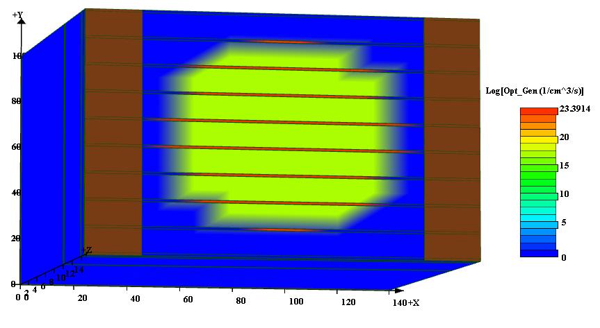
24 3D Optical Absorption/Generation 24

25 3D current magnitude 25

26 3D current magnitude y=14 26

27 3D current magnitude y=7 27
28 3D current magnitude y=0 28

29 From Plane 1 to Plane
30 From Plane 1 to Plane
31 Energy Band Diagram 31 z-direction
32 32 Incident Power at x=50 and y=70 z-
33 33 Optical Generation at x=50 and y=70 z- direction
34 Potential distribution at x=50 and y=70 34 z- direction
35 AM1.5 I-V Curve at T=300 K 35
36 Conclusion 36 2D & 3D simulations on compound single and multi-junction solar cells have been demonstrated. Non-local tunnel-junction model is calibrated with experiments Biased solar spectrum is used to obtain external quantum efficiency. Modeling results of I-V I V curve, Isc,, Voc & efficiency consistent with experimental results. Modeling results for multi-sun concentration are also presented: optimal sun number varies with contact pad separation, indicating different series resistance effect..
Simulation of silicon based thin-film solar cells. Copyright Crosslight Software Inc.
 Simulation of silicon based thin-film solar cells Copyright 1995-2008 Crosslight Software Inc. www.crosslight.com 1 Contents 2 Introduction Physical models & quantum tunneling Material properties Modeling
Modelling and Analysis of Four-Junction Tendem Solar Cell in Different Environmental Conditions Mr. Biraju J. Trivedi 1 Prof. Surendra Kumar Sriwas 2
 IJSRD - International Journal for Scientific Research & Development Vol. 3, Issue 08, 2015 ISSN (online): 2321-0613 Modelling and Analysis of Four-Junction Tendem Solar Cell in Different Environmental
Modeling of GaInP/GaAs Dual-Junction Solar Cells including Tunnel Junction
 Modeling of GaInP/GaAs Dual-Junction Solar Cells including Tunnel Junction Mathieu Baudrit and Carlos Algora Instituto de Energía Solar, Universidad Politécnica de Madrid, Spain mbaudrit@ies-def.upm.es
Solar Cell Parameters and Equivalent Circuit
 9 Solar Cell Parameters and Equivalent Circuit 9.1 External solar cell parameters The main parameters that are used to characterise the performance of solar cells are the peak power P max, the short-circuit
INCREASED CELL EFFICIENCY IN InGaAs THIN FILM SOLAR CELLS WITH DIELECTRIC AND METAL BACK REFLECTORS
 INCREASED CELL EFFICIENCY IN InGaAs THIN FILM SOLAR CELLS WITH DIELECTRIC AND METAL BACK REFLECTORS Koray Aydin, Marina S. Leite and Harry A. Atwater Thomas J. Watson Laboratories of Applied Physics, California
Design and Performance of InGaAs/GaAs Based Tandem Solar Cells
 American Journal of Engineering Research (AJER) e-issn: 2320-0847 p-issn : 2320-0936 Volume-5, Issue-11, pp-64-69 www.ajer.org Research Paper Open Access Design and Performance of InGaAs/GaAs Based Tandem
Photodiode: LECTURE-5
 LECTURE-5 Photodiode: Photodiode consists of an intrinsic semiconductor sandwiched between two heavily doped p-type and n-type semiconductors as shown in Fig. 3.2.2. Sufficient reverse voltage is applied
Ambition for the Future of Space Components from the Viewpoint of a Researcher in the Field of Space Solar Cells Masafumi Yamaguchi
 Ambition for the Future of Space Components from the Viewpoint of a Researcher in the Field of Space Solar Cells Masafumi Yamaguchi Toyota Technological Institute (Nagoya, Japan) Outline 1. Introduction
10/14/2009. Semiconductor basics pn junction Solar cell operation Design of silicon solar cell
 PHOTOVOLTAICS Fundamentals PV FUNDAMENTALS Semiconductor basics pn junction Solar cell operation Design of silicon solar cell SEMICONDUCTOR BASICS Allowed energy bands Valence and conduction band Fermi
MSE 410/ECE 340: Electrical Properties of Materials Fall 2016 Micron School of Materials Science and Engineering Boise State University
 MSE 410/ECE 340: Electrical Properties of Materials Fall 2016 Micron School of Materials Science and Engineering Boise State University Practice Final Exam 1 Read the questions carefully Label all figures
Key Questions ECE 340 Lecture 28 : Photodiodes
 Things you should know when you leave Key Questions ECE 340 Lecture 28 : Photodiodes Class Outline: How do the I-V characteristics change with illumination? How do solar cells operate? How do photodiodes
SHORT TECHNICAL DESCRIPTION
 Ioffe Physical-Technical Institute of Russian Academy of Sciences PV Laboratory 26 Polytechnicheskaya str., 194021 St-Petersburg, Russia tel: +7(812) 297-56-49, E-mail: vmandreev@mail.ioffe.ru FOUR-LAMP
What is the highest efficiency Solar Cell?
 What is the highest efficiency Solar Cell? GT CRC Roof-Mounted PV System Largest single PV structure at the time of it s construction for the 1996 Olympic games Produced more than 1 billion watt hrs. of
ECE 340 Lecture 29 : LEDs and Lasers Class Outline:
 ECE 340 Lecture 29 : LEDs and Lasers Class Outline: Light Emitting Diodes Lasers Semiconductor Lasers Things you should know when you leave Key Questions What is an LED and how does it work? How does a
Key Questions. What is an LED and how does it work? How does a laser work? How does a semiconductor laser work? ECE 340 Lecture 29 : LEDs and Lasers
 Things you should know when you leave Key Questions ECE 340 Lecture 29 : LEDs and Class Outline: What is an LED and how does it How does a laser How does a semiconductor laser How do light emitting diodes
NAME: Last First Signature
 UNIVERSITY OF CALIFORNIA, BERKELEY College of Engineering Department of Electrical Engineering and Computer Sciences EE 130: IC Devices Spring 2003 FINAL EXAMINATION NAME: Last First Signature STUDENT
PHYSICAL ELECTRONICS(ECE3540) APPLICATIONS OF PHYSICAL ELECTRONICS PART I
 APPLICATIONS OF PHYSICAL ELECTRONICS PART I") PHYSICAL ELECTRONICS(ECE3540) APPLICATIONS OF PHYSICAL ELECTRONICS PART I Tennessee Technological University Monday, October 28, 2013 1 Introduction In the following slides, we will discuss the summary
PHYSICAL ELECTRONICS(ECE3540) APPLICATIONS OF PHYSICAL ELECTRONICS PART I Tennessee Technological University Monday, October 28, 2013 1 Introduction In the following slides, we will discuss the summary
Evaluation of InGaP/InGaAs/Ge triple solar cell and optimization of solar structure focusing on series resista efficiency concentrator photovoltaic
 JAIST Reposi https://dspace.j Title Evaluation of InGaP/InGaAs/Ge triple solar cell and optimization of solar structure focusing on series resista efficiency concentrator photovoltaic Nishioka, K; Takamoto,
LEDs, Photodetectors and Solar Cells
 LEDs, Photodetectors and Solar Cells Chapter 7 (Parker) ELEC 424 John Peeples Why the Interest in Photons? Answer: Momentum and Radiation High electrical current density destroys minute polysilicon and
Lecture 18: Photodetectors
 Lecture 18: Photodetectors Contents 1 Introduction 1 2 Photodetector principle 2 3 Photoconductor 4 4 Photodiodes 6 4.1 Heterojunction photodiode.................... 8 4.2 Metal-semiconductor photodiode................
Chapter 1. Introduction
 Chapter 1 Introduction 1.1 Introduction of Device Technology Digital wireless communication system has become more and more popular in recent years due to its capability for both voice and data communication.
CHAPTER-2 Photo Voltaic System - An Overview
 CHAPTER-2 Photo Voltaic System - An Overview 15 CHAPTER-2 PHOTO VOLTAIC SYSTEM -AN OVERVIEW 2.1 Introduction With the depletion of traditional energies and the increase in pollution and greenhouse gases
Copyright 2006 Crosslight Software Inc. Analysis of Resonant-Cavity Light-Emitting Diodes
 Copyright 2006 Crosslight Software Inc. www.crosslight.com 1 Analysis of Resonant-Cavity Light-Emitting Diodes Contents About RCLED. Crosslight s model. Example of an InGaAs/AlGaAs RCLED with experimental
Fall 2004 Dawn Hettelsater, Yan Zhang and Ali Shakouri, 05/09/2002
 University of California at Santa Cruz Jack Baskin School of Engineering Electrical Engineering Department EE-145L: Properties of Materials Laboratory Lab 6: Solar Cells Fall 2004 Dawn Hettelsater, Yan
Semiconductor Devices Lecture 5, pn-junction Diode
 Semiconductor Devices Lecture 5, pn-junction Diode Content Contact potential Space charge region, Electric Field, depletion depth Current-Voltage characteristic Depletion layer capacitance Diffusion capacitance
15 Transit Time and Tunnel NDR Devices
 15 Transit Time and Tunnel NDR Devices Schematics of Transit-time NDR diode. A packet of carriers (e.g., electrons) is generated in a confined and narrow zone (generation region) and injected into the
Sub 300 nm Wavelength III-Nitride Tunnel-Injected Ultraviolet LEDs
 Sub 300 nm Wavelength III-Nitride Tunnel-Injected Ultraviolet LEDs Yuewei Zhang, Sriram Krishnamoorthy, Fatih Akyol, Sadia Monika Siddharth Rajan ECE, The Ohio State University Andrew Allerman, Michael
Optical Fiber Communication Lecture 11 Detectors
 Optical Fiber Communication Lecture 11 Detectors Warriors of the Net Detector Technologies MSM (Metal Semiconductor Metal) PIN Layer Structure Semiinsulating GaAs Contact InGaAsP p 5x10 18 Absorption InGaAs
Lab VIII Photodetectors ECE 476
 Lab VIII Photodetectors ECE 476 I. Purpose The electrical and optical properties of various photodetectors will be investigated. II. Background Photodiode A photodiode is a standard diode packaged so that
Quantum Condensed Matter Physics Lecture 16
 Quantum Condensed Matter Physics Lecture 16 David Ritchie QCMP Lent/Easter 2018 http://www.sp.phy.cam.ac.uk/drp2/home 16.1 Quantum Condensed Matter Physics 1. Classical and Semi-classical models for electrons
Project full title: "Nanowire based Tandem Solar Cells" Project acronym: Nano-Tandem Grant agreement no: Deliverable D6.1:
 Ref. Ares(2016)1038382-01/03/2016 Project full title: "Nanowire based Tandem Solar Cells" Project acronym: Nano-Tandem Grant agreement no: 641023 Deliverable D6.1: Report on adaption of EQE and IV measurement
CHAPTER 8 The PN Junction Diode
 CHAPTER 8 The PN Junction Diode Consider the process by which the potential barrier of a PN junction is lowered when a forward bias voltage is applied, so holes and electrons can flow across the junction
InP-based Waveguide Photodetector with Integrated Photon Multiplication
 InP-based Waveguide Photodetector with Integrated Photon Multiplication D.Pasquariello,J.Piprek,D.Lasaosa,andJ.E.Bowers Electrical and Computer Engineering Department University of California, Santa Barbara,
CHAPTER 8 The PN Junction Diode
 CHAPTER 8 The PN Junction Diode Consider the process by which the potential barrier of a PN junction is lowered when a forward bias voltage is applied, so holes and electrons can flow across the junction
1 Semiconductor-Photon Interaction
 1 SEMICONDUCTOR-PHOTON INTERACTION 1 1 Semiconductor-Photon Interaction Absorption: photo-detectors, solar cells, radiation sensors. Radiative transitions: light emitting diodes, displays. Stimulated emission:
UNIT IX ELECTRONIC DEVICES
 UNT X ELECTRONC DECES Weightage Marks : 07 Semiconductors Semiconductors diode-- characteristics in forward and reverse bias, diode as rectifier. - characteristics of LED, Photodiodes, solarcell and Zener
Davinci. Semiconductor Device Simulaion in 3D SYSTEMS PRODUCTS LOGICAL PRODUCTS PHYSICAL IMPLEMENTATION SIMULATION AND ANALYSIS LIBRARIES TCAD
 SYSTEMS PRODUCTS LOGICAL PRODUCTS PHYSICAL IMPLEMENTATION SIMULATION AND ANALYSIS LIBRARIES TCAD Aurora DFM WorkBench Davinci Medici Raphael Raphael-NES Silicon Early Access TSUPREM-4 Taurus-Device Taurus-Lithography
Review of Semiconductor Physics
 Review of Semiconductor Physics k B 1.38 u 10 23 JK -1 a) Energy level diagrams showing the excitation of an electron from the valence band to the conduction band. The resultant free electron can freely
Figure 1. Schematic diagram of a Fabry-Perot laser.
 Figure 1. Schematic diagram of a Fabry-Perot laser. Figure 1. Shows the structure of a typical edge-emitting laser. The dimensions of the active region are 200 m m in length, 2-10 m m lateral width and
Investigation of Photovoltaic Properties of In:ZnO/SiO 2 /p- Si Thin Film Devices
 Universities Research Journal 2011, Vol. 4, No. 4 Investigation of Photovoltaic Properties of In:ZnO/SiO 2 /p- Si Thin Film Devices Kay Thi Soe 1, Moht Moht Than 2 and Win Win Thar 3 Abstract This study
Intrinsic Semiconductor
 Semiconductors Crystalline solid materials whose resistivities are values between those of conductors and insulators. Good electrical characteristics and feasible fabrication technology are some reasons
Thin film PV Technologies III- V PV Technology
 Thin film PV Technologies III- V PV Technology Week 5.1 Arno Smets ` (Source: NASA) III V PV Technology Semiconductor Materials III- V semiconductors: GaAs: GaP: InP: InAs: GaInAs: GaInP: AlGaInAs: AlGaInP:
OPTOELECTRONIC and PHOTOVOLTAIC DEVICES
 OPTOELECTRONIC and PHOTOVOLTAIC DEVICES Outline 1. Introduction to the (semiconductor) physics: energy bands, charge carriers, semiconductors, p-n junction, materials, etc. 2. Light emitting diodes Light
Electronic devices-i. Difference between conductors, insulators and semiconductors
 Electronic devices-i Semiconductor Devices is one of the important and easy units in class XII CBSE Physics syllabus. It is easy to understand and learn. Generally the questions asked are simple. The unit
Microelectronic Circuits, Kyung Hee Univ. Spring, Bipolar Junction Transistors
 Bipolar Junction Transistors 1 Introduction physical structure of the bipolar transistor and how it works How the voltage between two terminals of the transistor controls the current that flows through
Solar Photovoltaic Cell Thermal Measurement Issues
 Solar Photovoltaic Cell Thermal Measurement Issues Bernie Siegal Thermal Engineering Associates, Inc. 2915 Copper Road Santa Clara, CA 95051 USA P: 650-961-5900 F: 650-227-3814 E: bsiegal@thermengr.com
ANISOTYPE GaAs BASED HETEROJUNCTIONS FOR III-V MULTIJUNCTION SOLAR CELLS
 ANISOTYPE Ga BASED HETEROJUNCTIONS FOR III-V MULTIJUNCTION SOLAR CELLS A.S. Gudovskikh 1,*, K.S. Zelentsov 1, N.A. Kalyuzhnyy 2, V.M. Lantratov 2, S.A. Mintairov 2 1 Saint-Petersburg Academic University
Measurement of Component Cell Current-Voltage Characteristics in a Tandem- Junction Two-Terminal Solar Cell
 Measurement of Component Cell Current-Voltage Characteristics in a Tandem- Junction Two-Terminal Solar Cell Chandan Das, Xianbi Xiang and Xunming Deng Department of Physics and Astronomy, University of
Voltage-dependent quantum efficiency measurements of amorphous silicon multijunction mini-modules
 Loughborough University Institutional Repository Voltage-dependent quantum efficiency measurements of amorphous silicon multijunction mini-modules This item was submitted to Loughborough University's Institutional
Design and Simulation of N-Substrate Reverse Type Ingaasp/Inp Avalanche Photodiode
 International Refereed Journal of Engineering and Science (IRJES) ISSN (Online) 2319-183X, (Print) 2319-1821 Volume 2, Issue 8 (August 2013), PP.34-39 Design and Simulation of N-Substrate Reverse Type
HIGH-EFFICIENCY MQW ELECTROABSORPTION MODULATORS
 HIGH-EFFICIENCY MQW ELECTROABSORPTION MODULATORS J. Piprek, Y.-J. Chiu, S.-Z. Zhang (1), J. E. Bowers, C. Prott (2), and H. Hillmer (2) University of California, ECE Department, Santa Barbara, CA 93106
LAB V. LIGHT EMITTING DIODES
 LAB V. LIGHT EMITTING DIODES 1. OBJECTIVE In this lab you are to measure I-V characteristics of Infrared (IR), Red and Blue light emitting diodes (LEDs). The emission intensity as a function of the diode
SILICON BASED COLOR PHOTOSENSITIVE CELLS WITH DEEP COLOR SEPARATION ON P + -P JUNCTIONS: CONSTRUCTIVE AND TECHNOLOGICAL DESIGN PROBLEMS
 SILICON BASED COLOR PHOTOSENSITIVE CELLS WITH DEEP COLOR SEPARATION ON P + -P JUNCTIONS: CONSTRUCTIVE AND TECHNOLOGICAL DESIGN PROBLEMS Gorshkova N.M., Dolgushin S.A. Unique IC's LLC, Moscow, Russia Institute
Session 10: Solid State Physics MOSFET
 Session 10: Solid State Physics MOSFET 1 Outline A B C D E F G H I J 2 MOSCap MOSFET Metal-Oxide-Semiconductor Field-Effect Transistor: Al (metal) SiO2 (oxide) High k ~0.1 ~5 A SiO2 A n+ n+ p-type Si (bulk)
Introduction to Photovoltaics
 Introduction to Photovoltaics PHYS 4400, Principles and Varieties of Solar Energy Instructor: Randy J. Ellingson The University of Toledo February 24, 2015 Only solar energy Of all the possible sources
Basic concepts. Optical Sources (b) Optical Sources (a) Requirements for light sources (b) Requirements for light sources (a)
 Optical Sources (a) Requirements for light sources (b) Requirements for light sources (a)") Optical Sources (a) Optical Sources (b) The main light sources used with fibre optic systems are: Light-emitting diodes (LEDs) Semiconductor lasers (diode lasers) Fibre laser and other compact solid-state
Optical Sources (a) Optical Sources (b) The main light sources used with fibre optic systems are: Light-emitting diodes (LEDs) Semiconductor lasers (diode lasers) Fibre laser and other compact solid-state
NAVAL POSTGRADUATE SCHOOL THESIS
 NAVAL POSTGRADUATE SCHOOL MONTEREY, CALIFORNIA THESIS MODELING RADIATION EFFECTS ON A TRIPLE JUNCTION SOLAR CELL USING SILVACO ATLAS by Daniel Schiavo June 2012 Thesis Advisor: Second Reader: Sherif Michael
Review Energy Bands Carrier Density & Mobility Carrier Transport Generation and Recombination
 Review Energy Bands Carrier Density & Mobility Carrier Transport Generation and Recombination Current Transport: Diffusion, Thermionic Emission & Tunneling For Diffusion current, the depletion layer is
Physics of Waveguide Photodetectors with Integrated Amplification
 Physics of Waveguide Photodetectors with Integrated Amplification J. Piprek, D. Lasaosa, D. Pasquariello, and J. E. Bowers Electrical and Computer Engineering Department University of California, Santa
Response of GaAs Photovoltaic Converters Under Pulsed Laser Illumination
 Response of GaAs Photovoltaic Converters Under Pulsed Laser Illumination TIQIANG SHAN 1, XINGLIN QI 2 The Third Department Mechanical Engineering College Shijiazhuang, Hebei CHINA stq0701@163.com 1, xinling399@163.com
Luminous Equivalent of Radiation
 Intensity vs λ Luminous Equivalent of Radiation When the spectral power (p(λ) for GaP-ZnO diode has a peak at 0.69µm) is combined with the eye-sensitivity curve a peak response at 0.65µm is obtained with
CONTENTS. 2.2 Schrodinger's Wave Equation 31. PART I Semiconductor Material Properties. 2.3 Applications of Schrodinger's Wave Equation 34
 CONTENTS Preface x Prologue Semiconductors and the Integrated Circuit xvii PART I Semiconductor Material Properties CHAPTER 1 The Crystal Structure of Solids 1 1.0 Preview 1 1.1 Semiconductor Materials
Università degli Studi di Roma Tor Vergata Dipartimento di Ingegneria Elettronica. Analogue Electronics. Paolo Colantonio A.A.
 Università degli Studi di Roma Tor Vergata Dipartimento di Ingegneria Elettronica Analogue Electronics Paolo Colantonio A.A. 2015-16 Introduction: materials Conductors e.g. copper or aluminum have a cloud
Chapter 6. Silicon-Germanium Technologies
 Chapter 6 licon-germanium Technologies 6.0 Introduction The design of bipolar transistors requires trade-offs between a number of parameters. To achieve a fast base transit time, hence achieving a high
Photovoltaic Cells for Optical Power and Data Transmission
 Photovoltaic Cells for Optical Power and Transmission H. Helmers, S.P. Philipps, S.K. Reichmuth, E. Oliva, D. Lackner, A.W. Bett Fraunhofer Institute for Solar Energy Systems ISE European Telemetry and
Title detector with operating temperature.
 Title Radiation measurements by a detector with operating temperature cryogen Kanno, Ikuo; Yoshihara, Fumiki; Nou Author(s) Osamu; Murase, Yasuhiro; Nakamura, Masaki Citation REVIEW OF SCIENTIFIC INSTRUMENTS
InP-based Waveguide Photodetector with Integrated Photon Multiplication
 InP-based Waveguide Photodetector with Integrated Photon Multiplication D.Pasquariello,J.Piprek,D.Lasaosa,andJ.E.Bowers Electrical and Computer Engineering Department University of California, Santa Barbara,
Electrical Characterization
 Listing and specification of characterization equipment at ISC Konstanz 30.05.2016 Electrical Characterization µw-pcd (Semilab) PV2000 (Semilab) - spatially resolved minority charge carrier lifetime -diffusion
Microelectronic Devices and Circuits Lecture 8 - BJTs Wrap-up, Solar Cells, LEDs - Outline
 6.012 - Microelectronic Devices and Circuits Lecture 8 - BJTs Wrap-up, Solar Cells, LEDs - Outline Announcements Exam One - Tomorrow, Wednesday, October 7, 7:30 pm BJT Review Wrapping up BJTs (for now)
Enhanced Emitter Transit Time for Heterojunction Bipolar Transistors (HBT)
") Advances in Electrical Engineering Systems (AEES)` 196 Vol. 1, No. 4, 2013, ISSN 2167-633X Copyright World Science Publisher, United States www.worldsciencepublisher.org Enhanced Emitter Transit Time for
Advances in Electrical Engineering Systems (AEES)` 196 Vol. 1, No. 4, 2013, ISSN 2167-633X Copyright World Science Publisher, United States www.worldsciencepublisher.org Enhanced Emitter Transit Time for
Research Article Modelling of Dual-Junction Solar Cells including Tunnel Junction
 Advances in Condensed Matter Physics Volume 2013, Article ID 546362, 5 pages http://dx.doi.org/10.1155/2013/546362 Research Article Modelling of Dual-Junction Solar Cells including Tunnel Junction Abdelaziz
Microscopic Basis for the Mechanism of Carrier Dynamics in an Operating p-n Junction Examined by using Light-Modulated Scanning Tunneling Spectroscopy
 Microscopic Basis for the Mechanism of Carrier Dynamics in an Operating p-n Junction Examined by using Light-Modulated Scanning Tunneling Spectroscopy Shoji Yoshida, Yuya Kanitani, Ryuji Oshima, Yoshitaka
SILICON NANOWIRE HYBRID PHOTOVOLTAICS
 SILICON NANOWIRE HYBRID PHOTOVOLTAICS Erik C. Garnett, Craig Peters, Mark Brongersma, Yi Cui and Mike McGehee Stanford Univeristy, Department of Materials Science, Stanford, CA, USA ABSTRACT Silicon nanowire
Esaki diodes in van der Waals heterojunctions with broken-gap energy band alignment
 Supplementary information for Esaki diodes in van der Waals heterojunctions with broken-gap energy band alignment Rusen Yan 1,2*, Sara Fathipour 2, Yimo Han 4, Bo Song 1,2, Shudong Xiao 1, Mingda Li 1,
Chap14. Photodiode Detectors
 Chap14. Photodiode Detectors Mohammad Ali Mansouri-Birjandi mansouri@ece.usb.ac.ir mamansouri@yahoo.com Faculty of Electrical and Computer Engineering University of Sistan and Baluchestan (USB) Design
INTRODUCING A NOVEL HIGH-EFFICIENCY ARC LESS HETEROUNCTION DJ SOLAR CELL
 FACTA UNIVERSITATIS Series:Electronics and Energetics Vol. 31, N o 1, March 2018, pp. 89-100 https://doi.org/10.2298/fuee1801089a INTRODUCING A NOVEL HIGH-EFFICIENCY ARC LESS HETEROUNCTION DJ SOLAR CELL
LAB V. LIGHT EMITTING DIODES
 LAB V. LIGHT EMITTING DIODES 1. OBJECTIVE In this lab you will measure the I-V characteristics of Infrared (IR), Red and Blue light emitting diodes (LEDs). Using a photodetector, the emission intensity
Department of Electrical Engineering IIT Madras
 Department of Electrical Engineering IIT Madras Sample Questions on Semiconductor Devices EE3 applicants who are interested to pursue their research in microelectronics devices area (fabrication and/or
Lecture 4. pn Junctions (Diodes) Wednesday 27/9/2017 pn junctions 1-1
 Wednesday 27/9/2017 pn junctions 1-1") Lecture 4 n Junctions (Diodes) Wednesday 27/9/2017 n junctions 1-1 Agenda Continue n junctions Equilibrium (zero bias) Deletion rejoins Built-in otential Reverse and forward bias I-V characteristics Bias
Lecture 4 n Junctions (Diodes) Wednesday 27/9/2017 n junctions 1-1 Agenda Continue n junctions Equilibrium (zero bias) Deletion rejoins Built-in otential Reverse and forward bias I-V characteristics Bias
Modeling Photonic Crystal Light Emitting Diode (PhCLED) Using APSYS. Copyright 2007 Crosslight Software Inc.
 Using APSYS. Copyright 2007 Crosslight Software Inc.") Modeling Photonic Crystal Light Emitting Diode (PhCLED) Using APSYS Copyright 2007 Crosslight Software Inc. www.crosslight.com 1 2 Model Contents A PhCLED with DBR An InGaN PhCLED with guided multimodes
Modeling Photonic Crystal Light Emitting Diode (PhCLED) Using APSYS Copyright 2007 Crosslight Software Inc. www.crosslight.com 1 2 Model Contents A PhCLED with DBR An InGaN PhCLED with guided multimodes
Introduction to semiconductor technology
 Introduction to semiconductor technology Outline 7 Field effect transistors MOS transistor current equation" MOS transistor channel mobility Substrate bias effect 7 Bipolar transistors Introduction Minority
Light Sources, Modulation, Transmitters and Receivers
 Optical Fibres and Telecommunications Light Sources, Modulation, Transmitters and Receivers Introduction Previous section looked at Fibres. How is light generated in the first place? How is light modulated?
SUPPLEMENTARY INFORMATION
 SUPPLEMENTARY INFORMATION Supplementary Information Real-space imaging of transient carrier dynamics by nanoscale pump-probe microscopy Yasuhiko Terada, Shoji Yoshida, Osamu Takeuchi, and Hidemi Shigekawa*
CHAPTER 8 The pn Junction Diode
 CHAPTER 8 The pn Junction Diode Consider the process by which the potential barrier of a pn junction is lowered when a forward bias voltage is applied, so holes and electrons can flow across the junction
Electronics I. Midterm #1
 EECS:3400 Electronics I s5ms_elct7.fm - Section Electronics I Midterm # Problems Points. 4 2. 5 3. 6 Total 5 Was the exam fair? yes no EECS:3400 Electronics I s5ms_elct7.fm - 2 Problem 4 points For full
14.2 Photodiodes 411
 14.2 Photodiodes 411 Maximum reverse voltage is specified for Ge and Si photodiodes and photoconductive cells. Exceeding this voltage can cause the breakdown and severe deterioration of the sensor s performance.
Characterisation of Photovoltaic Materials and Cells
 Standard Measurement Services and Prices No. Measurement Description Reference 1 Large area, 0.35-sun biased spectral response (SR) 2 Determination of linearity of spectral response with respect to irradiance
Electronics The basics of semiconductor physics
 Electronics The basics of semiconductor physics Prof. Márta Rencz, Gábor Takács BME DED 17/09/2015 1 / 37 The basic properties of semiconductors Range of conductivity [Source: http://www.britannica.com]
Lecture 14: Photodiodes
 Lecture 14: Photodiodes Background concepts p-n photodiodes photoconductive/photovoltaic modes p-i-n photodiodes responsivity and bandwidth Reading: Senior 8.1-8.8.3 Keiser Chapter 6 1 Electron-hole photogeneration
Optical Amplifiers. Continued. Photonic Network By Dr. M H Zaidi
 Optical Amplifiers Continued EDFA Multi Stage Designs 1st Active Stage Co-pumped 2nd Active Stage Counter-pumped Input Signal Er 3+ Doped Fiber Er 3+ Doped Fiber Output Signal Optical Isolator Optical
AIGaAs/InGaAIP Tunnel Junctions for Multifunction Solar Cells. Sharps, N. Y. Li, J. S. Hills, and H. Hou EMCORE Photovoltaics
 ,. P.R. Sharps EMCORE Photovoltaics 10420 Research Road SE Albuquerque, NM 87112 Phone: 505/332-5022 Fax: 505/332-5038 Paul_Sharps @emcore.com Category 4B Oral AIGaAs/InGaAIP Tunnel Junctions for Multifunction
Fundamentals of CMOS Image Sensors
 CHAPTER 2 Fundamentals of CMOS Image Sensors Mixed-Signal IC Design for Image Sensor 2-1 Outline Photoelectric Effect Photodetectors CMOS Image Sensor(CIS) Array Architecture CIS Peripherals Design Considerations
Advancements in solar simulators for Terrestrial solar cells at high concentration (500 to 5000 Suns) levels
 levels") Advancements in solar simulators for Terrestrial solar cells at high concentration (5 to 5 Suns) levels Doug Jungwirth, Lynne C. Eigler and Steve Espiritu Spectrolab, Inc., 5 Gladstone Avenue, Sylmar,
Advancements in solar simulators for Terrestrial solar cells at high concentration (5 to 5 Suns) levels Doug Jungwirth, Lynne C. Eigler and Steve Espiritu Spectrolab, Inc., 5 Gladstone Avenue, Sylmar,
EE Solar Cell Opreation. Y. Baghzouz Professor of Electrical Engineering
 EE 495-695 4.2 Solar Cell Opreation Y. Baghzouz Professor of Electrical Engineering Characteristic Resistance The characteristic resistance of a solar cell is the output resistance of the solar cell at
Solar Energy Materials & Solar Cells
 Solar Energy Materials & Solar Cells 134 (2015) 175 184 Contents lists available at ScienceDirect Solar Energy Materials & Solar Cells journal homepage: www.elsevier.com/locate/solmat Luminescent emission
31st European Photovoltaic Solar Energy Conference and Exhibition EFFECTS OF 10 MEV PROTON IRRADIATION OF III-V SOLAR CELLS
 EFFECTS OF 10 MEV PROTON IRRADIATION OF III-V SOLAR CELLS E. Yaccuzzi 1,2, M. Ochoa 3, M. Barrera 1,2, E. Barrigón 3, S. Rodriguez 1, P. Espinet 3, M.L. Ibarra 1,2, J. Garcia 1,2, E.M. Godfrin 1, M. Alurralde
Introduction to Optoelectronic Devices
 Introduction to Optoelectronic Devices Dr. Jing Bai Assistant Professor Department of Electrical and Computer Engineering University of Minnesota Duluth October 30th, 2012 1 Outline What is the optoelectronics?
Optical design of a low concentrator photovoltaic module
 Optical design of a low concentrator photovoltaic module MA Benecke*, JD Gerber, FJ Vorster and EE van Dyk Nelson Mandela Metropolitan University Centre for Renewable and Sustainable Energy Studies Abstract
C-V AND I-V MEASUREMENT SYSTEMS WINDOWS SOFTWARE
 C-V AND I-V MEASUREMENT SYSTEMS WINDOWS SOFTWARE Whether you require a simple C-V plotter to measure mobile ion contamination or an advanced system to measure multi-frequency C-V, I-V, TVS, or gate oxide
Substrate Bias Effects on Drain Induced Barrier Lowering (DIBL) in Short Channel NMOS FETs
 in Short Channel NMOS FETs") Australian Journal of Basic and Applied Sciences, 3(3): 1640-1644, 2009 ISSN 1991-8178 Substrate Bias Effects on Drain Induced Barrier Lowering (DIBL) in Short Channel NMOS FETs 1 1 1 1 2 A. Ruangphanit,
Australian Journal of Basic and Applied Sciences, 3(3): 1640-1644, 2009 ISSN 1991-8178 Substrate Bias Effects on Drain Induced Barrier Lowering (DIBL) in Short Channel NMOS FETs 1 1 1 1 2 A. Ruangphanit,