description/ordering information
|
|
|
- Claude Barnett
- 6 years ago
- Views:
Transcription
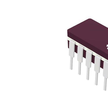
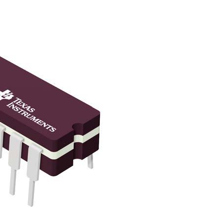
1 Dependable Texas Instruments Quality and Reliability description/ordering information These devices contain six independent inverters. SDLS029C DECEMBER 1983 REVISED JANUARY 2004 SN J PACKAGE SN54LS04, SN54S04... J OR W PACKAGE SN7404, SN74S04... D, N, OR NS PACKAGE SN74LS04... D, DB, N, OR NS PACKAGE (TOP VIEW) 1A 1Y 2A 2Y 3A 3Y GND V CC 6A 6Y 5A 5Y 4A 4Y SN W PACKAGE (TOP VIEW) 1A 2Y 2A V CC 3A 3Y 4A Y 6A 6Y GND 5Y 5A 4Y SN54LS04, SN54S04... FK PACKAGE (TOP VIEW) 2A NC 2Y NC 3A 1Y 1A NC Y GND NC VCC 4Y 4A 6A 6Y NC 5A NC 5Y NC No internal connection Please be aware that an important notice concerning availability, standard warranty, and use in critical applications of Texas Instruments semiconductor products and disclaimers thereto appears at the end of this data sheet. Copyright 2004, Texas Instruments Incorporated POST OFFICE BOX DALLAS, TEXAS
2 SDLS029C DECEMBER 1983 REVISED JANUARY 2004 TA 0 C to 70 C ORDERING INFORMATION PACKAGE ORDERABLE PART NUMBER TOP-SIDE MARKING Tube SN7404N SN7404N PDIP N Tube SN74LS04N SN74LS04N Tube SN74S04N SN74S04N Tube SN7404D Tape and reel SN7404DR 7404 Tube SN74LS04D SOIC D Tape and reel SN74LS04DR LS04 Tube Tape and reel SN74S04D SN74S04DR S04 Tape and reel SN7404NSR SN7404 SOP NS Tape and reel SN74LS04NSR 74LS04 Tape and reel SN74S04NSR 74S04 SSOP DB Tape and reel SN74LS04DBR LS04 CDIP J Tube SN5404J SN5404J Tube SNJ5404J SNJ5404J Tube SN54LS04J SN54LS04J Tube SN54S04J SN54S04J Tube SNJ54LS04J SNJ54LS04J 55 C to 125 C Tube SNJ54S04J SNJ54S04J Tube SNJ5404W SNJ5404W CFP W Tube SNJ54LS04W SNJ54LS04W LCCC FK Tube SNJ54S04W SNJ54S04W Tube SNJ54LS04FK SNJ54LS04FK Tube SNJ54S04FK SNJ54S04FK Package drawings, standard packing quantities, thermal data, symbolization, and PCB design guidelines are available at FUNCTION TABLE (each inverter) INPUT A H L OUTPUT Y L H 2 POST OFFICE BOX DALLAS, TEXAS 75265
3 SDLS029C DECEMBER 1983 REVISED JANUARY 2004 logic diagram (positive logic) 1A 1Y 2A 2Y 3A 3Y 4A 4Y 5A 5Y 6A 6Y Y = A POST OFFICE BOX DALLAS, TEXAS
4 SDLS029C DECEMBER 1983 REVISED JANUARY 2004 schematics (each gate) 04 VCC 4 kω 1.6 kω 130 Ω Input A Output Y 1 kω GND LS04 VCC S04 VCC 20 kω 8 kω 120 Ω 2.8 kω 900 Ω 50 Ω Input A 4 kω Output Y Input A 3.5 kω Output Y 12 kω 3 kω 500 Ω 250 Ω 1.5 kω GND GND Resistor values shown are nominal. 4 POST OFFICE BOX DALLAS, TEXAS 75265
5 SDLS029C DECEMBER 1983 REVISED JANUARY 2004 absolute maximum ratings over operating free-air temperature range (unless otherwise noted) Supply voltage, V CC (see Note 1) V Input voltage, V I : 04, S V LS V Package thermal impedance, θ JA (see Note 2): D package C/W DB package C/W N package C/W NS package C/W Storage temperature range, T stg C to 150 C Stresses beyond those listed under absolute maximum ratings may cause permanent damage to the device. This are stress ratings only, and functional operation of the device at these or any other conditions beyond those indicated under recommended operating conditions is not implied. Exposure to absolute-maximum-rated conditions for extended periods may affect device reliability. NOTES: 1. Voltage values are with respect to network ground terminal. 2. The package thermal impedance is calculated in accordance with JESD recommended operating conditions (see Note 3) SN5404 SN7404 UNIT MIN NOM MAX MIN NOM MAX VCC Supply voltage V VIH High-level input voltage 2 2 V VIL Low-level input voltage V IOH High-level output current ma IOL Low-level output current ma TA Operating free-air temperature C NOTE 3: All unused inputs of the device must be held at VCC or GND to ensure proper device operation. Refer to the TI application report, Implications of Slow or Floating CMOS Inputs, literature number SCBA004. electrical characteristics over recommended operating free-air temperature range (unless otherwise noted) PARAMETER TEST CONDITIONS SN5404 SN7404 MIN TYP MAX MIN TYP MAX VIK VCC = MIN, II = 12 ma V VOH VCC = MIN, VIL = 0.8 V, IOH = 0.4 ma V VOL VCC = MIN, VIH = 2 V, IOL = 16 ma V II VCC = MAX, VI = 5.5 V 1 1 ma IIH VCC = MAX, VI = 2.4 V µa IIL VCC = MAX, VI = 0.4 V ma IOS V CC = MAX ma ICCH VCC = MAX, VI = 0 V ma ICCL VCC = MAX, VI = 4.5 V ma For conditions shown as MIN or MAX, use the appropriate value specified under recommended operating conditions. All typical values are at VCC = 5 V, TA = 25 C. Not more than one output should be shorted at a time. UNIT POST OFFICE BOX DALLAS, TEXAS
6 SDLS029C DECEMBER 1983 REVISED JANUARY 2004 switching characteristics, V CC = 5 V, T A = 25 C (see Figure 1) PARAMETER tplh tphl FROM TO TEST CONDITIONS (INPUT) (OUTPUT) A Y RL = 400 Ω, CL = 15 pf SN5404 SN7404 MIN TYP MAX UNIT ns recommended operating conditions (see Note 3) SN54LS04 SN74LS04 MIN NOM MAX MIN NOM MAX VCC Supply voltage V VIH High-level input voltage 2 2 V VIL Low-level input voltage V IOH High-level output current ma IOL Low-level output current 4 8 ma TA Operating free-air temperature C NOTE 3: All unused inputs of the device must be held at VCC or GND to ensure proper device operation. Refer to the TI application report, Implications of Slow or Floating CMOS Inputs, literature number SCBA004. electrical characteristics over recommended operating free-air temperature range (unless otherwise noted) PARAMETER TEST CONDITIONS SN54LS04 SN74LS04 MIN TYP MAX MIN TYP MAX VIK VCC = MIN, II = 18 ma V VOH VCC = MIN, VIL = MAX, IOH = 0.4 ma V VOL VCC = MIN, VIH = 2 V IOL = 4 ma IOL = 8 ma II VCC = MAX, VI = 7 V ma IIH VCC = MAX, VI = 2.7 V µa IIL VCC = MAX, VI = 0.4 V ma IOS V CC = MAX ma ICCH VCC = MAX, VI = 0 V ma ICCL VCC = MAX, VI = 4.5 V ma For conditions shown as MIN or MAX, use the appropriate value specified under recommended operating conditions. All typical values are at VCC = 5 V, TA = 25 C. Not more than one output should be shorted at a time, and the duration of the short-circuit should not exceed one second. switching characteristics, V CC = 5 V, T A = 25 C (see Figure 2) UNIT UNIT V PARAMETER tplh tphl FROM TO TEST CONDITIONS (INPUT) (OUTPUT) A Y RL = 2 kω, CL = 15 pf SN54LS04 SN74LS04 MIN TYP MAX UNIT ns 6 POST OFFICE BOX DALLAS, TEXAS 75265
7 SDLS029C DECEMBER 1983 REVISED JANUARY 2004 recommended operating conditions (see Note 3) SN54S04 SN74S04 MIN NOM MAX MIN NOM MAX VCC Supply voltage V VIH High-level input voltage 2 2 V VIL Low-level input voltage V IOH High-level output current 1 1 ma IOL Low-level output current ma TA Operating free-air temperature C NOTE 3: All unused inputs of the device must be held at VCC or GND to ensure proper device operation. Refer to the TI application report, Implications of Slow or Floating CMOS Inputs, literature number SCBA004. electrical characteristics over recommended operating free-air temperature range (unless otherwise noted) PARAMETER TEST CONDITIONS SN54S04 SN74S04 MIN TYP MAX MIN TYP MAX VIK VCC = MIN, II = 18 ma V VOH VCC = MIN, VIL = 0.8 V, IOH = 1 ma V VOL VCC = MIN, VIH = 2 V, IOL = 20 ma V II VCC = MAX, VI = 5.5 V 1 1 ma IIH VCC = MAX, VI = 2.7 V µa IIL VCC = MAX, VI = 0.5 V 2 2 ma IOS V CC = MAX ma ICCH VCC = MAX, VI = 0 V ma ICCL VCC = MAX, VI = 4.5 V ma For conditions shown as MIN or MAX, use the appropriate value specified under recommended operating conditions. All typical values are at VCC = 5 V, TA = 25 C. Not more than one output should be shorted at a time, and the duration of the short-circuit should not exceed one second. switching characteristics, V CC = 5 V, T A = 25 C (see Figure 1) UNIT UNIT PARAMETER tplh tphl FROM TO TEST CONDITIONS (INPUT) (OUTPUT) A Y RL = 280 Ω, CL = 15 pf SN54S04 SN74S04 MIN TYP MAX UNIT ns tplh tphl A Y RL = 280 Ω, CL = 50 pf ns POST OFFICE BOX DALLAS, TEXAS
8 SDLS029C DECEMBER 1983 REVISED JANUARY 2004 PARAMETER MEASUREMENT INFORMATION SERIES 54/74 AND 54S/74S DEVICES From Output Under Test Test Point CL (see Note A) VCC RL (see Note B) From Output Under Test CL (see Note A) VCC RL Test Point VCC From Output Under Test CL (see Note A) Test Point RL 1 kω S1 (see Note B) S2 LOAD CIRCUIT FOR 2-STATE TOTEM-POLE OUTPUTS LOAD CIRCUIT FOR OPEN-COLLECTOR OUTPUTS LOAD CIRCUIT FOR 3-STATE OUTPUTS High-Level Pulse Low-Level Pulse 1.5 V 1.5 V tw 1.5 V 1.5 V VOLTAGE WAVEFORMS PULSE DURATIONS Timing Input Data Input tsu 1.5 V th 1.5 V 1.5 V VOLTAGE WAVEFORMS SETUP AND HOLD TIMES 3 V 0 V 3 V 0 V Input 1.5 V 1.5 V 3 V 0 V Output Control (low-level enabling) tpzl 1.5 V 1.5 V tplz 3 V 0 V In-Phase Output (see Note D) Out-of-Phase Output (see Note D) tplh tphl VOLTAGE WAVEFORMS PROPAGATION DELAY TIMES tphl 1.5 V 1.5 V tplh 1.5 V 1.5 V VOH VOL VOH VOL Waveform 1 (see Notes C and D) Waveform 2 (see Notes C and D) tpzh 1.5 V 1.5 V VOL V VOL tphz 1.5 V VOH VOH 0.5 V 1.5 V VOLTAGE WAVEFORMS ENABLE AND DISABLE TIMES, 3-STATE OUTPUTS NOTES: A. CL includes probe and jig capacitance. B. All diodes are 1N3064 or equivalent. C. Waveform 1 is for an output with internal conditions such that the output is low, except when disabled by the output control. Waveform 2 is for an output with internal conditions such that the output is high, except when disabled by the output control. D. S1 and S2 are closed for tplh, tphl, tphz, and tplz; S1 is open and S2 is closed for tpzh; S1 is closed and S2 is open for tpzl. E. All input pulses are supplied by generators having the following characteristics: PRR 1 MHz, ZO 50 Ω; tr and tf 7 ns for Series 54/74 devices and tr and tf 2.5 ns for Series 54S/74S devices. F. The outputs are measured one at a time, with one input transition per measurement. Figure 1. Load Circuits and Voltage Waveforms 8 POST OFFICE BOX DALLAS, TEXAS 75265
9 PARAMETER MEASUREMENT INFORMATION SERIES 54LS/74LS DEVICES SDLS029C DECEMBER 1983 REVISED JANUARY 2004 From Output Under Test Test Point CL (see Note A) VCC RL (see Note B) From Output Under Test CL (see Note A) VCC RL Test Point VCC From Output Under Test CL (see Note A) Test Point RL 5 kω S1 (see Note B) S2 LOAD CIRCUIT FOR 2-STATE TOTEM-POLE OUTPUTS LOAD CIRCUIT FOR OPEN-COLLECTOR OUTPUTS LOAD CIRCUIT FOR 3-STATE OUTPUTS High-Level Pulse Low-Level Pulse 1.3 V 1.3 V tw 1.3 V 1.3 V VOLTAGE WAVEFORMS PULSE DURATIONS Timing Input Data Input tsu 1.3 V th 1.3 V 1.3 V VOLTAGE WAVEFORMS SETUP AND HOLD TIMES 3 V 0 V 3 V 0 V Input 1.3 V 1.3 V 3 V 0 V Output Control (low-level enabling) tpzl 1.3 V 1.3 V tplz 3 V 0 V In-Phase Output (see Note D) Out-of-Phase Output (see Note D) tplh tphl VOLTAGE WAVEFORMS PROPAGATION DELAY TIMES tphl 1.3 V 1.3 V tplh 1.3 V 1.3 V VOH VOL VOH VOL Waveform 1 (see Notes C and D) Waveform 2 (see Notes C and D) NOTES: A. CL includes probe and jig capacitance. B. All diodes are 1N3064 or equivalent. C. Waveform 1 is for an output with internal conditions such that the output is low, except when disabled by the output control. Waveform 2 is for an output with internal conditions such that the output is high, except when disabled by the output control. D. S1 and S2 are closed for tplh, tphl, tphz, and tplz; S1 is open and S2 is closed for tpzh; S1 is closed and S2 is open for tpzl. E. Phase relationships between inputs and outputs have been chosen arbitrarily for these examples. F. All input pulses are supplied by generators having the following characteristics: PRR 1 MHz, ZO 50 Ω, tr 1.5 ns, tf 2.6 ns. G. The outputs are measured one at a time, with one input transition per measurement. tpzh 1.3 V Figure 2. Load Circuits and Voltage Waveforms 1.3 V VOL V VOL tphz 1.5 V VOH VOH 0.5 V 1.5 V VOLTAGE WAVEFORMS ENABLE AND DISABLE TIMES, 3-STATE OUTPUTS POST OFFICE BOX DALLAS, TEXAS
10 PACKAGE OPTION ADDENDUM 17-Mar-2017 PACKAGING INFORMATION Orderable Device Status (1) Package Type Package Drawing Pins Package Qty Eco Plan (2) Lead/Ball Finish (6) MSL Peak Temp (3) Op Temp ( C) JM38510/00105BCA ACTIVE CDIP J 14 1 TBD A42 N / A for Pkg Type -55 to 125 JM38510/ 00105BCA JM38510/00105BDA ACTIVE CFP W 14 1 TBD A42 N / A for Pkg Type -55 to 125 JM38510/ 00105BDA JM38510/07003BCA ACTIVE CDIP J 14 1 TBD A42 N / A for Pkg Type -55 to 125 JM38510/ 07003BCA JM38510/07003BDA ACTIVE CFP W 14 1 TBD A42 N / A for Pkg Type -55 to 125 JM38510/ 07003BDA JM38510/30003B2A ACTIVE LCCC FK 20 1 TBD POST-PLATE N / A for Pkg Type -55 to 125 JM38510/ 30003B2A JM38510/30003BCA ACTIVE CDIP J 14 1 TBD A42 N / A for Pkg Type -55 to 125 JM38510/ 30003BCA JM38510/30003BDA ACTIVE CFP W 14 1 TBD A42 N / A for Pkg Type -55 to 125 JM38510/ 30003BDA JM38510/30003SCA ACTIVE CDIP J TBD A42 N / A for Pkg Type -55 to 125 JM38510/ 30003SCA M38510/00105BCA ACTIVE CDIP J 14 1 TBD A42 N / A for Pkg Type -55 to 125 JM38510/ 00105BCA M38510/00105BDA ACTIVE CFP W 14 1 TBD A42 N / A for Pkg Type -55 to 125 JM38510/ 00105BDA M38510/07003BCA ACTIVE CDIP J 14 1 TBD A42 N / A for Pkg Type -55 to 125 JM38510/ 07003BCA M38510/07003BDA ACTIVE CFP W 14 1 TBD A42 N / A for Pkg Type -55 to 125 JM38510/ 07003BDA M38510/30003B2A ACTIVE LCCC FK 20 1 TBD POST-PLATE N / A for Pkg Type -55 to 125 JM38510/ 30003B2A M38510/30003BCA ACTIVE CDIP J 14 1 TBD A42 N / A for Pkg Type -55 to 125 JM38510/ 30003BCA M38510/30003BDA ACTIVE CFP W 14 1 TBD A42 N / A for Pkg Type -55 to 125 JM38510/ 30003BDA M38510/30003SCA ACTIVE CDIP J TBD A42 N / A for Pkg Type -55 to 125 JM38510/ 30003SCA SN5404J ACTIVE CDIP J 14 1 TBD A42 N / A for Pkg Type -55 to 125 SN5404J Device Marking (4/5) Samples Addendum-Page 1
11 PACKAGE OPTION ADDENDUM 17-Mar-2017 Orderable Device Status (1) Package Type Package Drawing Pins Package Qty Eco Plan (2) Lead/Ball Finish (6) MSL Peak Temp (3) Op Temp ( C) SN54LS04J ACTIVE CDIP J 14 1 TBD A42 N / A for Pkg Type -55 to 125 SN54LS04J Device Marking (4/5) Samples SN54S04J ACTIVE CDIP J 14 1 TBD A42 N / A for Pkg Type -55 to 125 SN54S04J SN7404D ACTIVE SOIC D Green (RoHS SN7404DE4 ACTIVE SOIC D Green (RoHS SN7404DG4 ACTIVE SOIC D Green (RoHS SN7404DR ACTIVE SOIC D Green (RoHS SN7404N ACTIVE PDIP N Pb-Free (RoHS) SN7404NE4 ACTIVE PDIP N Pb-Free (RoHS) SN74LS04D ACTIVE SOIC D Green (RoHS SN74LS04DBR ACTIVE SSOP DB Green (RoHS SN74LS04DG4 ACTIVE SOIC D Green (RoHS SN74LS04DR ACTIVE SOIC D Green (RoHS SN74LS04DRE4 ACTIVE SOIC D Green (RoHS SN74LS04DRG4 ACTIVE SOIC D Green (RoHS SN74LS04N ACTIVE PDIP N Pb-Free (RoHS) SN74LS04NE4 ACTIVE PDIP N Pb-Free (RoHS) SN74LS04NSR ACTIVE SO NS Green (RoHS SN74LS04NSRG4 ACTIVE SO NS Green (RoHS CU NIPDAU Level-1-260C-UNLIM 0 to CU NIPDAU Level-1-260C-UNLIM 0 to CU NIPDAU Level-1-260C-UNLIM 0 to CU NIPDAU Level-1-260C-UNLIM 0 to CU NIPDAU N / A for Pkg Type 0 to 70 SN7404N CU NIPDAU N / A for Pkg Type 0 to 70 SN7404N CU NIPDAU Level-1-260C-UNLIM 0 to 70 LS04 CU NIPDAU Level-1-260C-UNLIM LS04 CU NIPDAU Level-1-260C-UNLIM 0 to 70 LS04 CU NIPDAU Level-1-260C-UNLIM 0 to 70 LS04 CU NIPDAU Level-1-260C-UNLIM 0 to 70 LS04 CU NIPDAU Level-1-260C-UNLIM 0 to 70 LS04 CU NIPDAU N / A for Pkg Type 0 to 70 SN74LS04N CU NIPDAU N / A for Pkg Type 0 to 70 SN74LS04N CU NIPDAU Level-1-260C-UNLIM 0 to 70 74LS04 CU NIPDAU Level-1-260C-UNLIM 0 to 70 74LS04 Addendum-Page 2
12 PACKAGE OPTION ADDENDUM 17-Mar-2017 Orderable Device Status (1) Package Type Package Drawing Pins Package Qty Eco Plan SN74S04D ACTIVE SOIC D Green (RoHS SN74S04DG4 ACTIVE SOIC D Green (RoHS SN74S04DR ACTIVE SOIC D Green (RoHS SN74S04N ACTIVE PDIP N Pb-Free (RoHS) SN74S04NE4 ACTIVE PDIP N Pb-Free (RoHS) SN74S04NSR ACTIVE SO NS Green (RoHS (2) Lead/Ball Finish (6) MSL Peak Temp (3) Op Temp ( C) CU NIPDAU Level-1-260C-UNLIM 0 to 70 S04 CU NIPDAU Level-1-260C-UNLIM 0 to 70 S04 CU NIPDAU Level-1-260C-UNLIM 0 to 70 S04 CU NIPDAU N / A for Pkg Type 0 to 70 SN74S04N CU NIPDAU N / A for Pkg Type 0 to 70 SN74S04N CU NIPDAU Level-1-260C-UNLIM 0 to 70 74S04 SNJ5404J ACTIVE CDIP J 14 1 TBD A42 N / A for Pkg Type -55 to 125 SNJ5404J Device Marking (4/5) Samples SNJ5404W ACTIVE CFP W 14 1 TBD A42 N / A for Pkg Type -55 to 125 SNJ5404W SNJ54LS04FK ACTIVE LCCC FK 20 1 TBD POST-PLATE N / A for Pkg Type -55 to 125 SNJ54LS 04FK SNJ54LS04J ACTIVE CDIP J 14 1 TBD A42 N / A for Pkg Type -55 to 125 SNJ54LS04J SNJ54LS04W ACTIVE CFP W 14 1 TBD A42 N / A for Pkg Type -55 to 125 SNJ54LS04W SNJ54S04FK ACTIVE LCCC FK 20 1 TBD POST-PLATE N / A for Pkg Type -55 to 125 SNJ54S 04FK SNJ54S04J ACTIVE CDIP J 14 1 TBD A42 N / A for Pkg Type -55 to 125 SNJ54S04J SNJ54S04W ACTIVE CFP W 14 1 TBD A42 N / A for Pkg Type -55 to 125 SNJ54S04W (1) The marketing status values are defined as follows: ACTIVE: Product device recommended for new designs. LIFEBUY: TI has announced that the device will be discontinued, and a lifetime-buy period is in effect. NRND: Not recommended for new designs. Device is in production to support existing customers, but TI does not recommend using this part in a new design. PREVIEW: Device has been announced but is not in production. Samples may or may not be available. OBSOLETE: TI has discontinued the production of the device. (2) Eco Plan - The planned eco-friendly classification: Pb-Free (RoHS), Pb-Free (RoHS Exempt), or Green (RoHS - please check for the latest availability information and additional product content details. TBD: The Pb-Free/Green conversion plan has not been defined. Addendum-Page 3
13 PACKAGE OPTION ADDENDUM 17-Mar-2017 Pb-Free (RoHS): TI's terms "Lead-Free" or "Pb-Free" mean semiconductor products that are compatible with the current RoHS requirements for all 6 substances, including the requirement that lead not exceed 0.1% by weight in homogeneous materials. Where designed to be soldered at high temperatures, TI Pb-Free products are suitable for use in specified lead-free processes. Pb-Free (RoHS Exempt): This component has a RoHS exemption for either 1) lead-based flip-chip solder bumps used between the die and package, or 2) lead-based die adhesive used between the die and leadframe. The component is otherwise considered Pb-Free (RoHS compatible) as defined above. Green (RoHS : TI defines "Green" to mean Pb-Free (RoHS compatible), and free of Bromine (Br) and Antimony (Sb) based flame retardants (Br or Sb do not exceed 0.1% by weight in homogeneous material) (3) MSL, Peak Temp. - The Moisture Sensitivity Level rating according to the JEDEC industry standard classifications, and peak solder temperature. (4) There may be additional marking, which relates to the logo, the lot trace code information, or the environmental category on the device. (5) Multiple Device Markings will be inside parentheses. Only one Device Marking contained in parentheses and separated by a "~" will appear on a device. If a line is indented then it is a continuation of the previous line and the two combined represent the entire Device Marking for that device. (6) Lead/Ball Finish - Orderable Devices may have multiple material finish options. Finish options are separated by a vertical ruled line. Lead/Ball Finish values may wrap to two lines if the finish value exceeds the maximum column width. Important Information and Disclaimer:The information provided on this page represents TI's knowledge and belief as of the date that it is provided. TI bases its knowledge and belief on information provided by third parties, and makes no representation or warranty as to the accuracy of such information. Efforts are underway to better integrate information from third parties. TI has taken and continues to take reasonable steps to provide representative and accurate information but may not have conducted destructive testing or chemical analysis on incoming materials and chemicals. TI and TI suppliers consider certain information to be proprietary, and thus CAS numbers and other limited information may not be available for release. In no event shall TI's liability arising out of such information exceed the total purchase price of the TI part(s) at issue in this document sold by TI to Customer on an annual basis. OTHER QUALIFIED VERSIONS OF SN5404, SN54LS04, SN54LS04-SP, SN54S04, SN7404, SN74LS04, SN74S04 : Catalog: SN7404, SN74LS04, SN54LS04, SN74S04 Military: SN5404, SN54LS04, SN54S04 Space: SN54LS04-SP NOTE: Qualified Version Definitions: Catalog - TI's standard catalog product Military - QML certified for Military and Defense Applications Addendum-Page 4
14 PACKAGE OPTION ADDENDUM 17-Mar-2017 Space - Radiation tolerant, ceramic packaging and qualified for use in Space-based application Addendum-Page 5
15 PACKAGE MATERIALS INFORMATION 10-Sep-2015 TAPE AND REEL INFORMATION *All dimensions are nominal Device Package Type Package Drawing Pins SPQ Reel Diameter (mm) Reel Width W1 (mm) A0 (mm) B0 (mm) K0 (mm) P1 (mm) W (mm) Pin1 Quadrant SN7404DR SOIC D Q1 SN74LS04DBR SSOP DB Q1 SN74LS04DR SOIC D Q1 SN74S04DR SOIC D Q1 SN74S04NSR SO NS Q1 Pack Materials-Page 1
16 PACKAGE MATERIALS INFORMATION 10-Sep-2015 *All dimensions are nominal Device Package Type Package Drawing Pins SPQ Length (mm) Width (mm) Height (mm) SN7404DR SOIC D SN74LS04DBR SSOP DB SN74LS04DR SOIC D SN74S04DR SOIC D SN74S04NSR SO NS Pack Materials-Page 2
17
18
19
20
21 SCALE PACKAGE OUTLINE J0014A CDIP mm max height CERAMIC DUAL IN LINE PACKAGE PIN 1 ID (OPTIONAL) A 4X.005 MIN [0.13] TYP [ ] 12X.100 [2.54] X [ ] 14X [ ].010 [0.25] C A B [ ] 7 8 B [ ] [ ] AT GAGE PLANE.2 MAX TYP [5.08] C.13 MIN TYP [3.3] SEATING PLANE.015 GAGE PLANE [0.38] 0-15 TYP 14X [ ] /A 05/2017 NOTES: 1. All controlling linear dimensions are in inches. Dimensions in brackets are in millimeters. Any dimension in brackets or parenthesis are for reference only. Dimensioning and tolerancing per ASME Y14.5M. 2. This drawing is subject to change without notice. 3. This package is hermitically sealed with a ceramic lid using glass frit. 4. Index point is provided on cap for terminal identification only and on press ceramic glass frit seal only. 5. Falls within MIL-STD-1835 and GDIP1-T14.
22 J0014A EXAMPLE BOARD LAYOUT CDIP mm max height CERAMIC DUAL IN LINE PACKAGE SEE DETAIL A (.300 ) TYP [7.62] SEE DETAIL B X (.100 ) [2.54] SYMM 14X (.039) [1] 7 8 SYMM LAND PATTERN EXAMPLE NON-SOLDER MASK DEFINED SCALE: 5X.002 MAX [0.05] ALL AROUND (.063) [1.6] SOLDER MASK OPENING METAL (.063) [1.6] METAL (R.002 ) TYP [0.05] DETAIL A SCALE: 15X SOLDER MASK OPENING DETAIL B 13X, SCALE: 15X.002 MAX [0.05] ALL AROUND /A 05/2017
23
24
25
26 MECHANICAL DATA MSSO002E JANUARY 1995 REVISED DECEMBER 2001 DB (R-PDSO-G**) 28 PINS SHOWN PLASTIC SMALL-OUTLINE 0,65 0,38 0,22 0,15 M ,60 5,00 8,20 7,40 0,25 0,09 Gage Plane ,25 A 0 8 0,95 0,55 2,00 MAX 0,05 MIN Seating Plane 0,10 DIM PINS ** A MAX 6,50 6,50 7,50 8,50 10,50 10,50 12,90 A MIN 5,90 5,90 6,90 7,90 9,90 9,90 12, /E 12/01 NOTES: A. All linear dimensions are in millimeters. B. This drawing is subject to change without notice. C. Body dimensions do not include mold flash or protrusion not to exceed 0,15. D. Falls within JEDEC MO-150 POST OFFICE BOX DALLAS, TEXAS 75265
27 IMPORTANT NOTICE Texas Instruments Incorporated (TI) reserves the right to make corrections, enhancements, improvements and other changes to its semiconductor products and services per JESD46, latest issue, and to discontinue any product or service per JESD48, latest issue. Buyers should obtain the latest relevant information before placing orders and should verify that such information is current and complete. TI s published terms of sale for semiconductor products ( apply to the sale of packaged integrated circuit products that TI has qualified and released to market. Additional terms may apply to the use or sale of other types of TI products and services. Reproduction of significant portions of TI information in TI data sheets is permissible only if reproduction is without alteration and is accompanied by all associated warranties, conditions, limitations, and notices. TI is not responsible or liable for such reproduced documentation. Information of third parties may be subject to additional restrictions. Resale of TI products or services with statements different from or beyond the parameters stated by TI for that product or service voids all express and any implied warranties for the associated TI product or service and is an unfair and deceptive business practice. TI is not responsible or liable for any such statements. Buyers and others who are developing systems that incorporate TI products (collectively, Designers ) understand and agree that Designers remain responsible for using their independent analysis, evaluation and judgment in designing their applications and that Designers have full and exclusive responsibility to assure the safety of Designers' applications and compliance of their applications (and of all TI products used in or for Designers applications) with all applicable regulations, laws and other applicable requirements. Designer represents that, with respect to their applications, Designer has all the necessary expertise to create and implement safeguards that (1) anticipate dangerous consequences of failures, (2) monitor failures and their consequences, and (3) lessen the likelihood of failures that might cause harm and take appropriate actions. Designer agrees that prior to using or distributing any applications that include TI products, Designer will thoroughly test such applications and the functionality of such TI products as used in such applications. TI s provision of technical, application or other design advice, quality characterization, reliability data or other services or information, including, but not limited to, reference designs and materials relating to evaluation modules, (collectively, TI Resources ) are intended to assist designers who are developing applications that incorporate TI products; by downloading, accessing or using TI Resources in any way, Designer (individually or, if Designer is acting on behalf of a company, Designer s company) agrees to use any particular TI Resource solely for this purpose and subject to the terms of this Notice. TI s provision of TI Resources does not expand or otherwise alter TI s applicable published warranties or warranty disclaimers for TI products, and no additional obligations or liabilities arise from TI providing such TI Resources. TI reserves the right to make corrections, enhancements, improvements and other changes to its TI Resources. TI has not conducted any testing other than that specifically described in the published documentation for a particular TI Resource. Designer is authorized to use, copy and modify any individual TI Resource only in connection with the development of applications that include the TI product(s) identified in such TI Resource. NO OTHER LICENSE, EXPRESS OR IMPLIED, BY ESTOPPEL OR OTHERWISE TO ANY OTHER TI INTELLECTUAL PROPERTY RIGHT, AND NO LICENSE TO ANY TECHNOLOGY OR INTELLECTUAL PROPERTY RIGHT OF TI OR ANY THIRD PARTY IS GRANTED HEREIN, including but not limited to any patent right, copyright, mask work right, or other intellectual property right relating to any combination, machine, or process in which TI products or services are used. Information regarding or referencing third-party products or services does not constitute a license to use such products or services, or a warranty or endorsement thereof. Use of TI Resources may require a license from a third party under the patents or other intellectual property of the third party, or a license from TI under the patents or other intellectual property of TI. TI RESOURCES ARE PROVIDED AS IS AND WITH ALL FAULTS. TI DISCLAIMS ALL OTHER WARRANTIES OR REPRESENTATIONS, EXPRESS OR IMPLIED, REGARDING RESOURCES OR USE THEREOF, INCLUDING BUT NOT LIMITED TO ACCURACY OR COMPLETENESS, TITLE, ANY EPIDEMIC FAILURE WARRANTY AND ANY IMPLIED WARRANTIES OF MERCHANTABILITY, FITNESS FOR A PARTICULAR PURPOSE, AND NON-INFRINGEMENT OF ANY THIRD PARTY INTELLECTUAL PROPERTY RIGHTS. TI SHALL NOT BE LIABLE FOR AND SHALL NOT DEFEND OR INDEMNIFY DESIGNER AGAINST ANY CLAIM, INCLUDING BUT NOT LIMITED TO ANY INFRINGEMENT CLAIM THAT RELATES TO OR IS BASED ON ANY COMBINATION OF PRODUCTS EVEN IF DESCRIBED IN TI RESOURCES OR OTHERWISE. IN NO EVENT SHALL TI BE LIABLE FOR ANY ACTUAL, DIRECT, SPECIAL, COLLATERAL, INDIRECT, PUNITIVE, INCIDENTAL, CONSEQUENTIAL OR EXEMPLARY DAMAGES IN CONNECTION WITH OR ARISING OUT OF TI RESOURCES OR USE THEREOF, AND REGARDLESS OF WHETHER TI HAS BEEN ADVISED OF THE POSSIBILITY OF SUCH DAMAGES. Unless TI has explicitly designated an individual product as meeting the requirements of a particular industry standard (e.g., ISO/TS and ISO 26262), TI is not responsible for any failure to meet such industry standard requirements. Where TI specifically promotes products as facilitating functional safety or as compliant with industry functional safety standards, such products are intended to help enable customers to design and create their own applications that meet applicable functional safety standards and requirements. Using products in an application does not by itself establish any safety features in the application. Designers must ensure compliance with safety-related requirements and standards applicable to their applications. Designer may not use any TI products in life-critical medical equipment unless authorized officers of the parties have executed a special contract specifically governing such use. Life-critical medical equipment is medical equipment where failure of such equipment would cause serious bodily injury or death (e.g., life support, pacemakers, defibrillators, heart pumps, neurostimulators, and implantables). Such equipment includes, without limitation, all medical devices identified by the U.S. Food and Drug Administration as Class III devices and equivalent classifications outside the U.S. TI may expressly designate certain products as completing a particular qualification (e.g., Q100, Military Grade, or Enhanced Product). Designers agree that it has the necessary expertise to select the product with the appropriate qualification designation for their applications and that proper product selection is at Designers own risk. Designers are solely responsible for compliance with all legal and regulatory requirements in connection with such selection. Designer will fully indemnify TI and its representatives against any damages, costs, losses, and/or liabilities arising out of Designer s noncompliance with the terms and provisions of this Notice. Mailing Address: Texas Instruments, Post Office Box , Dallas, Texas Copyright 2017, Texas Instruments Incorporated
SN5406, SN5416, SN7406, SN7416 HEX INVERTER BUFFERS/DRIVERS WITH OPEN-COLLECTOR HIGH-VOLTAGE OUTPUTS SDLS031A DECEMBER 1983 REVISED DECEMBER 2001
 SN5406, SN5416, SN7406, SN7416 HEX INVERTER BUFFERS/DRIVERS WITH OPEN-COLLECTOR HIGH-VOLTAGE OUTPUTS SDLS031A DECEMBER 1983 REVISED DECEMBER 2001 Convert TTL Voltage Levels to MOS Levels High Sink-Current
SN5404, SN54LS04, SN54S04, SN7404, SN74LS04, SN74S04 HEX INVERTERS
 Dependable Texas Instruments Quality and Reliability description These devices contain six independent inverters. SN5404, SN54LS04, SN54S04, SN5404... J PACKAGE SN54LS04, SN54S04... J OR W PACKAGE SN7404...
description/ordering information
 The SN5405 is obsolete and no longer is supplied. Package Options Include Plastic Small-Outline (D, NS), Shrink Small-Outline (DB), and Ceramic Flat (W) Packages, Ceramic Chip Carriers (FK), and Standard
SN5406, SN5416, SN7406, SN7416 HEX INVERTER BUFFERS/DRIVERS WITH OPEN-COLLECTOR HIGH-VOLTAGE OUTPUTS
 Convert TTL Voltage Levels to MOS Levels High Sink-Current Capability Input Clamping Diodes Simplify System Design Open-Collector Drivers for Indicator Lamps and Relays Inputs Fully Compatible With Most
SN5404, SN54LS04, SN54S04, SN7404, SN74LS04, SN74S04 HEX INVERTERS
 Dependable Texas Instruments Quality and Reliability description These devices contain six independent inverters. SN404, SN4LS04, SN4S04, SN404... J PACKAGE SN4LS04, SN4S04... J OR W PACKAGE SN7404...
SN54ALS32, SN54AS32, SN74ALS32, SN74AS32 QUADRUPLE 2-INPUT POSITIVE-OR GATES
 SN54ALS32, SN54AS32, SN74ALS32, SN74AS32 QUADRUPLE 2-INPUT POSITIVE-OR GATES SDAS113B APRIL 1982 REVISED DECEMBER 1994 Package Options Include Plastic Small-Outline (D) Packages, Ceramic Chip Carriers
description/ordering information
 Dependable Texas Instruments Quality and Reliability description/ordering information These devices contain six independent inverters. SDLS029C DECEMBER 1983 REVISED JANUARY 2004 SN5404... J PACKAGE SN54LS04,
description/ordering information
 Dependable Texas Instruments Quality and Reliability description/ordering information These devices contain six independent inverters. SN5404... J PACKAGE SN54LS04, SN54S04... J OR W PACKAGE SN7404, SN74S04...
SN54ALS09, SN74ALS09 QUADRUPLE 2-INPUT POSITIVE-AND GATES WITH OPEN-COLLECTOR OUTPUTS
 SN54ALS09, SN74ALS09 QUADRUPLE 2-INPUT POSITIVE-AND GATES WITH OPEN-COLLECTOR OUTPUTS SDAS084B APRIL 1982 REVISED DECEMBER 1994 Package Options Include Plastic Small-Outline (D) Packages, Ceramic Chip
description logic diagram (positive logic) logic symbol
 logic symbol") SDAS074B APRIL 1982 REVISED JANUARY 1995 AS1004A Offer High Capacitive-Drive Capability Driver Version of ALS04B and AS04 Package Options Include Plastic Small-Outline (D) Packages, Ceramic Chip Carriers
SDAS074B APRIL 1982 REVISED JANUARY 1995 AS1004A Offer High Capacitive-Drive Capability Driver Version of ALS04B and AS04 Package Options Include Plastic Small-Outline (D) Packages, Ceramic Chip Carriers
SN54ALS38B, SN74ALS38B QUADRUPLE 2-INPUT POSITIVE-NAND BUFFERS WITH OPEN-COLLECTOR OUTPUTS
 SN54ALS38B, SN74ALS38B QUADRUPLE 2-INPUT POSITIVE-NAND BUFFERS WITH OPEN-COLLECTOR OUTPUTS SDAS196B APRIL 1982 REVISED DECEMBER 1994 Package Options Include Plastic Small-Outline (D) Packages, Ceramic
SN5414, SN54LS14, SN7414, SN74LS14 HEX SCHMITT-TRIGGER INVERTERS
 Operation From Very Slow Edges Improved Line-Receiving Characteristics High Noise Immunity SN5414, SN54LS14, SN5414, SN54LS14...J OR W PACKAGE SN7414... D, N, OR NS PACKAGE SN74LS14... D, DB, OR N PACKAGE
EN: This Datasheet is presented by the m anufacturer. Please v isit our website for pricing and availability at ore.hu.
 EN: This Datasheet is presented by the m anufacturer. Please v isit our website for pricing and availability at www.hest ore.hu. Convert TTL Voltage Levels to MOS Levels High Sink-Current Capability Clamping
 Distributed by: www.jameco.com 1-800-831-4242 The content and copyrights of the attached material are the property of its owner. Package Options Include Plastic Small-Outline (D, NS, PS), Shrink Small-Outline
description 1G 1A1 2Y4 1A2 2Y3 1A3 2Y2 1A4 2Y1 GND V CC 2G/2G 1Y1 2A4 1Y2 2A3 1Y3 2A2 1Y4 2A1 1Y1 2A4 1Y2 2A3 1Y3 1A2 2Y3 1A3 2Y2 1A4 2A2 2G/2G 2Y1
 SN54LS240, SN54LS241, SN54LS244, SN54S240, SN54S241, SN54S244 3-State s Drive Bus Lines or Buffer Memory Address Registers PNP s Reduce DC Loading Hysteresis at s Improves Noise Margins description These
description logic diagram (positive logic) logic symbol
 logic symbol") SDAS112B APRIL 1982 REVISED DECEMBER 1994 Package Options Include Plastic Small-Outline (D) Packages, Ceramic Chip Carriers (FK), and Standard Plastic (N) and Ceramic (J) 300-mil DIPs description These
SDAS112B APRIL 1982 REVISED DECEMBER 1994 Package Options Include Plastic Small-Outline (D) Packages, Ceramic Chip Carriers (FK), and Standard Plastic (N) and Ceramic (J) 300-mil DIPs description These
SN75150 DUAL LINE DRIVER
 SN75150 DUAL LINE DRIVER Meets or Exceeds the Requirement of TIA/EIA-232-F and ITU Recommendation V.28 Withstands Sustained Output Short Circuit to Any Low-Impedance Voltage Between 25 V and 25 V 2-µs
SN54LS373, SN54LS374, SN54S373, SN54S374, SN74LS373, SN74LS374, SN74S373, SN74S374 OCTAL D-TYPE TRANSPARENT LATCHES AND EDGE-TRIGGERED FLIP-FLOPS
 SN54LS373, SN54LS374, SN54S373, SN54S374, SN74LS373, SN74LS374, SN74S373, SN74S374 OCTAL D-TYPE TRANSPARENT LATCHES AND EDGE-TRIGGERED FLIP-FLOPS SDLS165B OCTOBER 1975 REVISED AUGUST 2002 Choice of Eight
description logic symbol
 SDAS187A APRIL 1982 REVISED DECEMBER 1994 Package Options Include Plastic Small-Outline (D) Packages, Ceramic Chip Carriers (FK), and Standard Plastic (N) and Ceramic (J) 300-mil DIPs description These
SN5414, SN54LS14, SN7414, SN74LS14 HEX SCHMITT-TRIGGER INVERTERS
 Operation From Very Slow Edges Improved Line-Receiving Characteristics High Noise Immunity SN5414, SN54LS14, SN5414, SN54LS14...J OR W PACKAGE SN7414... D, N, OR NS PACKAGE SN74LS14... D, DB, OR N PACKAGE
SN54ALS139, SN74ALS139 DUAL 2-LINE TO 4-LINE DECODERS/DEMULTIPLEXERS
 SN54ALS9, SN74ALS9 DUAL 2-LINE TO 4-LINE DECODERS/DEMULTIPLEXERS Designed Specifically for High-Speed Memory Decoders and Data Transmission Systems Incorporate Two Enable Inputs to Simplify Cascading and/or
description logic diagram (positive logic) logic symbol
 logic symbol") SDAS074B APRIL 1982 REVISED JANUARY 1995 AS1004A Offer High Capacitive-Drive Capability Driver Version of ALS04B and AS04 Package Options Include Plastic Small-Outline (D) Packages, Ceramic Chip Carriers
SDAS074B APRIL 1982 REVISED JANUARY 1995 AS1004A Offer High Capacitive-Drive Capability Driver Version of ALS04B and AS04 Package Options Include Plastic Small-Outline (D) Packages, Ceramic Chip Carriers
SN54LS06, SN74LS06, SN74LS16 HEX INVERTER BUFFERS/DRIVERS WITH OPEN-COLLECTOR HIGH-VOLTAGE OUTPUTS
 Convert TTL Voltage Levels to MOS Levels High Sink-Current Capability Clamping Diodes Simplify System Design Open-Collector Driver for Indicator Lamps and Relays s Fully Compatible With Most TTL Circuits
SN75471 THRU SN75473 DUAL PERIPHERAL DRIVERS
 SN747 THRU SN747 DUAL PERIPHERAL DRIVERS SLRS024 DECEMBER 976 REVISED MAY 990 PERIPHERAL DRIVERS FOR HIGH-VOLTAGE HIGH-CURRENT DRIVER APPLICATIONS Characterized for Use to 00 ma High-Voltage Outputs No
SN54ALS32, SN54AS32, SN74ALS32, SN74AS32 QUADRUPLE 2-INPUT POSITIVE-OR GATES
 SN54ALS32, SN54AS32, SN74ALS32, SN74AS32 QUADRUPLE 2-INPUT POSITIVE-OR GATES SDAS113B APRIL 1982 REVISED DECEMBER 1994 Package Options Include Plastic Small-Outline (D) Packages, Ceramic Chip Carriers
 PACKAGE OPTION ADDENDUM www.ti.com 17-Mar-2017 PACKAGING INFORMATION Orderable Device Status (1) Package Type Package Drawing Pins Package Qty Eco Plan (2) Lead/Ball Finish (6) MSL Peak Temp (3) Op Temp
description logic diagram (positive logic) logic symbol
 logic symbol") SDAS063B APRIL 1982 REVISED DECEMBER 1994 Package Options Include Plastic Small-Outline (D) Packages, Ceramic Chip Carriers (FK), and Standard Plastic (N) and Ceramic (J) 300-mil DIPs description These
SDAS063B APRIL 1982 REVISED DECEMBER 1994 Package Options Include Plastic Small-Outline (D) Packages, Ceramic Chip Carriers (FK), and Standard Plastic (N) and Ceramic (J) 300-mil DIPs description These
description/ordering information
 2-V to 6-V V CC Operation Inputs Accept Voltages to 6 V Max t pd of 9 ns at 5 V SN54AC86... J OR W PACKAGE SN74AC86... D, DB, N, NS, OR PW PACKAGE (TOP VIEW) 1A 1B 1Y 2A 2B 2Y GND 1 2 3 4 5 6 7 14 13 12
SN54LS245, SN74LS245 OCTAL BUS TRANSCEIVERS WITH 3-STATE OUTPUTS
 3-State s Drive Bus Lines Directly PNP s Reduce dc Loading on Bus Lines Hysteresis at Bus s Improves Noise Margins Typical Propagation Delay Times Port to Port, 8 ns TYPE IOL (SINK CURRENT) IOH (SOURCE
SN74CBT3861DWR 10-BIT FET BUS SWITCH. description. logic diagram (positive logic)
") SN74CBT3861 10-BIT FET BUS SWITCH SCDS061D APRIL 1998 REVISED OCTOBER 2000 5-Ω Switch Connection Between Two Ports TTL-Compatible Input Levels Latch-Up Performance Exceeds 250 ma Per JESD 17 description
SN74CBT3861 10-BIT FET BUS SWITCH SCDS061D APRIL 1998 REVISED OCTOBER 2000 5-Ω Switch Connection Between Two Ports TTL-Compatible Input Levels Latch-Up Performance Exceeds 250 ma Per JESD 17 description
These devices contain four independent 2-input NAND gates. The devices perform the Boolean function Y = A B or Y = A + B in positive logic.
 Package Options Include Plastic Small-Outline (D, NS, PS), Shrink Small-Outline (DB), and Ceramic Flat (W) Packages, Ceramic Chip Carriers (FK), and Standard Plastic (N) and Ceramic (J) DIPs SN5400...J
ua9637ac DUAL DIFFERENTIAL LINE RECEIVER
 ua9637ac DUAL DIFFERENTIAL LINE RECEIVER Meets or Exceeds the Requirements of ANSI Standards EIA/TIA-422-B and EIA/TIA-423-B and ITU Recommendations V.10 and V.11 Operates From Single 5-V Power Supply
description/ordering information
 SCAS528D AUGUST 1995 REVISED OCTOBER 2003 2-V to 6-V V CC Operation Inputs Accept Voltages to 6 V Max t pd of 7.5 ns at 5 V SN54AC32...J OR W PACKAGE SN74AC32... D, DB, N, NS, OR PW PACKAGE (TOP VIEW)
SN54LS373, SN54LS374, SN54S373, SN54S374, SN74LS373, SN74LS374, SN74S373, SN74S374 OCTAL D-TYPE TRANSPARENT LATCHES AND EDGE-TRIGGERED FLIP-FLOPS
 SN54LS373, SN54LS374, SN54S373, SN54S374, SN74LS373, SN74LS374, SN74S373, SN74S374 OCTAL D-TYPE TRANSPARENT LATCHES AND EDGE-TRIGGERED FLIP-FLOPS SDLS165B OCTOBER 1975 REVISED AUGUST 2002 Choice of Eight
SN54LS373, SN54LS374, SN54S373, SN54S374, SN74LS373, SN74LS374, SN74S373, SN74S374 OCTAL D-TYPE TRANSPARENT LATCHES AND EDGE-TRIGGERED FLIP-FLOPS
 Choice of Eight Latches or Eight D-Type Flip-Flops in a Single Package 3-State Bus-Driving Outputs Full Parallel Access for Loading Buffered Control Inputs Clock-Enable Input Has Hysteresis to Improve
ORDERING INFORMATION ORDERABLE PART NUMBER SN74CBTS3306PWR
 5-Ω Switch Connection Between Two Ports TTL-Compatible Input Levels description/ordering information The SN74CBTS3306 features independent line switches with Schottky diodes on the I/Os to clamp undershoot.
These devices contain four independent 2-input NAND gates. The devices perform the Boolean function Y = A B or Y = A + B in positive logic.
 Package Optio Include Plastic Small-Outline (D, NS, PS), Shrink Small-Outline (D), and Ceramic Flat (W) Packages, Ceramic Chip Carriers (FK), and Standard Plastic (N) and Ceramic (J) DIPs SN00...J PCKGE
These devices contain four independent 2-input NAND gates. The devices perform the Boolean function Y = A B or Y = A + B in positive logic.
 Package Options Include Plastic Small-Outline (D, NS, PS), Shrink Small-Outline (DB), and Ceramic Flat (W) Packages, Ceramic Chip Carriers (FK), and Standard Plastic (N) and Ceramic (J) DIPs SN5400...J
SN54125, SN54126, SN54LS125A, SN54LS126A, SN74125, SN74126, SN74LS125A, SN74LS126A QUADRUPLE BUS BUFFERS WITH 3-STATE OUTPUTS
 The SN54125, SN54126, SN74125, SN74126, and SN54LS126A are obsolete and are no longer supplied. Quad Bus Buffers 3-State Outputs Separate Control for Each Channel description These bus buffers feature
Data sheet acquired from Harris Semiconductor SCHS083B Revised March 2003
 Data sheet acquired from Harris Semiconductor SCHS083B Revised March 2003 The CD4536B types are supplied in 16-lead hermetic dual-in-line ceramic packages (F3A suffix), 16-lead dual-in-line plastic packages
SN5414, SN54LS14, SN7414, SN74LS14 HEX SCHMITT-TRIGGER INVERTERS
 Operation From Very Slow Edges Improved Line-Receiving Characteristics High Noise Immunity SN5414, SN54LS14, SN5414, SN54LS14...J OR W PACKAGE SN7414... D, N, OR NS PACKAGE SN74LS14... D, DB, OR N PACKAGE
1OE 1Y1 1A1 1A2 1Y2 1Y3 1A3 1A4 1Y4 2OE 2Y1 2A1 2Y2 2A2 2A3 2Y3 2Y4 2A4 POST OFFICE BOX DALLAS, TEXAS 75265
 SDAS040B DECEMBER 983 REVISED JANUARY 995 Open-Collector Outputs Drive Bus Lines or Buffer Memory Address Registers Eliminate the Need for 3-State Overlap Protection pnp Inputs Reduce dc Loading Open-Collector
SN75157 DUAL DIFFERENTIAL LINE RECEIVER
 SN75157 DUAL DIFFERENTIAL LINE RECEIVER Meets or Exceeds the Requirements of ANSI Standards EIA/TIA-422-B and EIA/TIA-423-B and ITU Recommendation V.1 and V.11 Operates From Single 5-V Power Supply Wide
These devices contain four independent 2-input NAND gates. The devices perform the Boolean function Y = A B or Y = A + B in positive logic.
 Package Options Include Plastic Small-Outline (D, NS, PS), Shrink Small-Outline (DB), and Ceramic Flat (W) Packages, Ceramic Chip Carriers (FK), and Standard Plastic (N) and Ceramic (J) DIPs SN5400...J
SN54LS373, SN54LS374, SN54S373, SN54S374, SN74LS373, SN74LS374, SN74S373, SN74S374 OCTAL D-TYPE TRANSPARENT LATCHES AND EDGE-TRIGGERED FLIP-FLOPS
 SN54LS373, SN54LS374, SN54S373, SN54S374, SN74LS373, SN74LS374, SN74S373, SN74S374 OCTAL D-TYPE TRANSPARENT LATCHES AND EDGE-TRIGGERED FLIP-FLOPS SDLS165B OCTOBER 1975 REVISED AUGUST 2002 Choice of Eight
SN75158 DUAL DIFFERENTIAL LINE DRIVER
 SN7558 DUAL DIFFERENTIAL LINE DRIVER Meets or Exceeds the Requirements of ANSI EIA/TIA-422-B and ITU Recommendation V. Single 5-V Supply Balanced-Line Operation TTL Compatible High Output Impedance in
CD54AC04, CD74AC04 HEX INVERTERS
 CD54AC04, CD74AC04 HEX INVERTERS AC Types Feature 1.5-V to 5.5-V Operation and Balanced Noise Immunity at 30% of the Supply Voltage Speed of Bipolar F, AS, and S, With Significantly Reduced Power Consumption
SN54ALS05A, SN74ALS05A HEX INVERTERS WITH OPEN-COLLECTOR OUTPUTS
 SN54ALS05A, SN74ALS05A HEX INVERTERS WITH OPEN-COLLECTOR OUTPUTS SDAS190A APRIL 1982 REVISED DECEMBER 1994 Package Options Include Plastic Small-Outline (D) Packages, Ceramic Chip Carriers (FK), and Standard
SN54AC04, SN74AC04 HEX INVERTERS
 SN54AC04, SN74AC04 HEX INVERTERS 2-V to 6-V V CC Operation Inputs Accept Voltages to 6 V Max t pd of 7 ns at 5 V SN54AC04...J OR W PACKAGE SN74AC04...D, DB, N, NS, OR PW PACKAGE (TOP VIEW) 1A 1Y 2A 2Y
description/ordering information
 AC Types Feature 1.5-V to 5.5-V Operation and Balanced Noise Immunity at 30% of the Supply Speed of Bipolar F, AS, and S, With Significantly Reduced Power Consumption Balanced Propagation Delays ±24-mA
MC3486 QUADRUPLE DIFFERENTIAL LINE RECEIVER WITH 3-STATE OUTPUTS
 Meets or Exceeds the Requirements of ANSI Standards EIA/TIA-422-B and EIA/TIA-423-B and ITU Recommendations V.10 and V.11 3-State, TTL-Compatible s Fast Transition Times Operates From Single 5-V Supply
ORDERING INFORMATION PACKAGE
 5-Ω Switch Connection Between Two Ports TTL-Compatible Input Levels Designed to Be Used in Level-Shifting Applications description/ordering information The SN74CBTD3861 provides ten bits of high-speed
SN54AS885, SN74AS885 8-BIT MAGNITUDE COMPARATORS
 SNAS, SNAS -BIT MAGNITUDE COMPARATORS Latchable P-Input Ports With Power-Up Clear Choice of Logical or Arithmetic (Two s Complement) Comparison Data and Inputs Utilize pnp Input Transistors to Reduce dc
CD54ACT20, CD74ACT20 DUAL 4-INPUT POSITIVE-NAND GATES
 CD54ACT20, CD74ACT20 DUAL 4-INPUT POSITIVE-NAND GATES Inputs Are TTL-Voltage Compatible Speed of Bipolar F, AS, and S, With Significantly Reduced Power Consumption Balanced Propagation Delays ±24-mA Output
SN54ALS1035, SN74ALS1035 HEX NONINVERTING BUFFERS WITH OPEN-COLLECTOR OUTPUTS
 Noninverting Buffers With Open-Collector Outputs description These devices contain six independent noninverting buffers. They perform the Boolean function Y = A. The open-collector outputs require pullup
74ACT11245 OCTAL BUS TRANSCEIVER WITH 3-STATE OUTPUTS
 74ACT11245 OCTAL BUS TRANSCEIVER WITH 3-STATE OUTPUTS SCAS031C JULY 1987 REVISED APRIL 1996 3-State Outputs Drive Bus Lines Directly Inputs Are TTL-Voltage Compatible Flow-Through Architecture Optimizes
SN54173, SN54LS173A, SN74173, SN74LS173A 4-BIT D-TYPE REGISTERS WITH 3-STATE OUTPUTS
 3-State Outputs Interface Directly With System Bus Gated Output-Control LInes for Enabling or Disabling the Outputs Fully Independent Clock Virtually Eliminates Restrictions for Operating in One of Two
SN74LV04A-Q1 HEX INVERTER
 SN74LV04A-Q1 HEX INVERTER Qualified for Automotive Applications ESD Protection Exceeds 2000 V Per MIL-STD-883, Method 3015; Exceeds 200 V Using Machine Model (C = 200 pf, R = 0) 2-V to 5.5-V Operation
SN54ALS174, SN54ALS175, SN54AS174, SN54AS175B SN74ALS174, SN74ALS175, SN74AS174, SN74AS175B HEX/QUADRUPLE D-TYPE FLIP-FLOPS WITH CLEAR
 ALS174 and AS174 Contain Six Flip-Flops With Single-Rail Outputs ALS175 and AS175B Contain Four Flip-Flops With Double-Rail Outputs Buffered Clock and Direct-Clear Inputs SN54ALS174, SN54ALS175, SN54AS174,
DS8830, SN55183, SN75183 DUAL DIFFERENTIAL LINE DRIVERS
 DS8830, SN5583, SN7583 DUAL DIFFERENTIAL LINE DRIVERS Single 5-V Supply Differential Line Operation Dual Channels T TL Compatibility Short-Circuit Protection of Outputs Output Clamp Diodes to Terminate
74ACT11244 OCTAL BUFFER/LINE DRIVER WITH 3-STATE OUTPUTS
 3-State Outputs Drive Bus Lines or Buffer Memory Address Registers Inputs Are TTL-Voltage Compatible Flow-Through Architecture Optimizes PCB Layout Center-Pin V CC and GND Configurations to Minimize High-Speed
description/ordering information
 Supports Mixed-Mode Signal Operation (5-V Input and Output Voltages With 3.3-V V CC ) Supports Unregulated Battery Operation Down to 2.7 V Typical V OLP (Output Ground Bounce)
SN54ALS138A, SN54AS138, SN74ALS138A, SN74AS138 3-LINE TO 8-LINE DECODERS/DEMULTIPLEXERS
 SN54ALS138A, SN54AS138, SN74ALS138A, SN74AS138 3-LINE TO 8-LINE DECODERS/DEMULTIPLEXERS Designed Specifically for High-Speed Memory Decoders and Data Transmission Systems Incorporate Three Enable Inputs
CD54ACT112, CD74ACT112 DUAL J-K NEGATIVE-EDGE-TRIGGERED FLIP-FLOPS WITH CLEAR AND PRESET
 Inputs Are TTL-Voltage Compatible Speed of Bipolar F, AS, and S, With Significantly Reduced Power Consumption Balanced Propagation Delays ±24-mA Output Drive Current Fanout to 15 F Devices SCR-Latchup-Resistant
SN54HCT540, SN74HCT540 OCTAL BUFFERS AND LINE DRIVERS WITH 3-STATE OUTPUTS
 Operating Voltage Range of 4.5 V to 5.5 V Low Power Consumption, 80-µA Max I CC Typical t pd = 12 ns ±6-mA Output Drive at 5 V Low Input Current of 1 µa Max Inputs Are TTL-Voltage Compatible High-Current
SN54LS07, SN74LS07, SN74LS17 HEX BUFFERS/DRIVERS WITH OPEN-COLLECTOR HIGH-VOLTAGE OUTPUTS
 Convert TTL Voltage Levels to MOS Levels High Sink-Current Capability Clamping Diodes Simplify System Design Open-Collector Driver for Indicator Lamps and Relays description These hex buffers/drivers feature
CD74HC4017-Q1 HIGH-SPEED CMOS LOGIC DECADE COUNTER/DIVIDER WITH 10 DECODED OUTPUTS
 Qualified for Automotive Applications Fully Static Operation Buffered Inputs Common Reset Positive Edge Clocking Typical f MAX = 60 MHz at = 5 V, = 5 pf, T A = 25 C Fanout (Over Temperature Range) Standard
SN75124 TRIPLE LINE RECEIVER
 SN75124 TRIPLE LINE RECEIER Meets or Exceeds the Requirements of IBM System 360 Input/Output Interface Specification Operates From Single 5- Supply TTL Compatible Built-In Input Threshold Hysteresis High
description CLR SR SER A B C D SL SER GND V CC Q A Q B Q C Q D CLK S1 S0 SR SER CLR CLK SL SER GND
 Parallel-to-Serial, Serial-to-Parallel Conversions Left or Right Shifts Parallel Synchronous Loading Direct Overriding Clear Temporary Data-Latching Capability Package Options Include Plastic Small-Outline
description/ordering information
 SCLS087E DECEMBER 1982 REVISED AUGUST 2003 Wide Operating Voltage Range of 2 V to 6 V Outputs Can Drive Up To 10 LSTTL Loads Low Power Consumption, 20-µA Max I CC Typical t pd = 11 ns ±4-mA Output Drive
1 to 4 Configurable Clock Buffer for 3D Displays
 1 S3 GND S4 4 5 6 CLKIN 3 CLKOUT3 S1 2 Top View CLKOUT4 S2 1 7 8 9 OE 12 11 10 CLKOUT1 VDD CLKOUT2 CDC1104 SCAS921 SEPTEMBER 2011 1 to 4 Configurable Clock Buffer for 3D Displays Check for Samples: CDC1104
CD54HCT258, CD74HCT258 QUADRUPLE 2-LINE TO 1-LINE SELECTORS/MULTIPLEXERS WITH 3-STATE OUTPUTS
 4.5-V to 5.5-V V CC Operation Wide Operating Temperature Range of 55 C to 125 C Balanced Propagation Delays and Transition Times Standard Outputs Drive Up To 10 LS-TTL Loads Significant Power Reduction
description/ordering information
 µ SLVS060K JUNE 1976 REVISED APRIL 2005 3-Terminal Regulators Output Current Up To 500 ma No External Components High Power-Dissipation Capability Internal Short-Circuit Current Limiting Output Transistor
description/ordering information
 The SN74LS16 is obsolete and is no longer supplied. Convert TTL Voltage Levels to MOS Levels High Sink-Current Capability Input Clamping Diodes Simplify System Design Open-Collector Driver for Indicator
description/ordering information
 Operating Voltage Range of 4.5 V to 5.5 V High-Current 3-State True Outputs Can Drive Up To 15 LSTTL Loads Low Power Consumption, 80-µA Max I CC Typical t pd = 22 ns ±6-mA Output Drive at 5 V Low Input
ORDERING INFORMATION. SOIC DW Tape and reel SN74CBT3384ADWR
 SN74CBT3384A 10-BIT FET BUS SWITCH SCDS004L NOVEMBER 1992 REVISED JANUARY 2004 5-Ω Switch Connection Between Two Ports TTL-Compatible Input Levels description/ordering information The SN74CBT3384A provides
ORDERING INFORMATION T A PACKAGE ORDERABLE PART NUMBER. SOIC D Tape and reel SN74CBTD3306DR 40 C to85 C
 5-Ω Switch Connection Between Two Ports TTL-Compatible Input Levels Designed to Be Used in Level-Shifting Applications description/ordering information The SN74CBTD3306 features two independent line switches.
AVAILABLE OPTIONS PACKAGE VIOmax SMALL OUTLINE. PLASTIC DIP at 25 C (D) (P) 0 C to 70 C 5 mv LM306D LM306P
 (P) 0 C to 70 C 5 mv LM306D LM306P") SLCS8A OCTOBER 979 REVISED OCTOBER 99 Fast Response Times Improved Gain and Accuracy Fanout to Series 5/7 TTL Loads Strobe Capability Short-Circuit and Surge Protection Designed to Be Interchangeable With
SLCS8A OCTOBER 979 REVISED OCTOBER 99 Fast Response Times Improved Gain and Accuracy Fanout to Series 5/7 TTL Loads Strobe Capability Short-Circuit and Surge Protection Designed to Be Interchangeable With
SN54ACT16244, 74ACT BIT BUFFERS/LINE DRIVERS WITH 3-STATE OUTPUTS
 Members of the Texas Instruments Widebus Family Inputs Are TTL-Voltage Compatible 3-State Outputs Drive Bus Lines or Buffer Memory Address Registers Flow-Through Architecture Optimizes PCB Layout Distributed
description/ordering information
 5-Ω Switch Connection Between Two Ports TTL-Compatible Input Levels SN54CBTD3384...JT OR W PACKAGE SN74CBTD3384... DB, DBQ, DGV, DW, OR PW PACKAGE (TOP VIEW) 1OE 1B1 1A1 1A2 1B2 1B3 1A3 1A4 1B4 1B5 1A5
description/ordering information
 Wide Operating Voltage Range of 2 V to 6 V High-Current 3-State Outputs Drive Bus Lines, Buffer Memory Address Registers, or Drive Up To 15 LSTTL Loads True Outputs Low Power Consumption, 80-µA Max I CC
SN54LS373, SN54LS374, SN54S373, SN54S374, SN74LS373, SN74LS374, SN74S373, SN74S374 OCTAL D-TYPE TRANSPARENT LATCHES AND EDGE-TRIGGERED FLIP-FLOPS
 SN54LS373, SN54LS374, SN54S373, SN54S374, SN74LS373, SN74LS374, SN74S373, SN74S374 OCTAL D-TYPE TRANSPARENT LATCHES AND EDGE-TRIGGERED FLIP-FLOPS SDLS165B OCTOBER 1975 REVISED AUGUST 2002 Choice of Eight
description/ordering information
 SLLS094C SEPTEMBER 1983 REVISED MAY 2004 Meet or Exceed the Requirements of ANSI TIA/ EIA-232-E and ITU Recommendation V.28 Current-Limited Output: 10 ma Typical Power-Off Output Impedance: 300 Ω Minimum
This device contains a single 2-input NOR gate that performs the Boolean function Y = A B or Y = A + B in positive logic. ORDERING INFORMATION
 SN74AHCT1G02 SINGLE 2-INPUT POSITIVE-NOR GATE SCLS341K APRIL 1996 REVISED FEBRUARY 2003 Operating Range of 4.5 V to 5.5 V Max t pd of 6.5 ns at 5 V Low Power Consumption, 10-µA Max I CC ±8-mA Output Drive
AVAILABLE OPTIONS PACKAGE SMALL OUTLINE (D) The D package is available taped and reeled. Add the suffix R to the device type (i.e., LT1030CDR).
 The D package is available taped and reeled. Add the suffix R to the device type (i.e., LT1030CDR).") LT1030C QUADRUPLE LOW-POWER LINE DRIVER Low Supply Voltage... ±5 V to ±15 V Supply Current...500 µa Typical Zero Supply Current When Shut Down Outputs Can Be Driven ±30 V Output Open When Off (3-State)
LT1030C QUADRUPLE LOW-POWER LINE DRIVER Low Supply Voltage... ±5 V to ±15 V Supply Current...500 µa Typical Zero Supply Current When Shut Down Outputs Can Be Driven ±30 V Output Open When Off (3-State)
SN54HC652, SN74HC652 OCTAL BUS TRANSCEIVERS AND REGISTERS WITH 3-STATE OUTPUTS
 Wide Operating Voltage Range of 2 V to 6 V High-Current 3-State Outputs Can Drive Up To 15 LSTTL Loads Low Power Consumption, 80-µA Max I CC Typical t pd = 11 ns ±6-mA Output Drive at 5 V SN54HC652...JT
GENERAL-PURPOSE LOW-VOLTAGE COMPARATORS
 1 LMV331-Q1 SINGLE, LMV393-Q1 DUAL SLOS468D MAY 2005 REVISED AUGUST 2011 GENERAL-PURPOSE LOW-VOLTAGE COMPARATORS Check for Samples: LMV331-Q1 SINGLE, LMV393-Q1 DUAL 1FEATURES Qualified for Automotive Applications
Data sheet acquired from Harris Semiconductor SCHS038C Revised October 2003
 Data sheet acquired from Harris Semiconductor SCHS038C Revised October 2003 The CD4035B types are supplied in 16-lead hermetic dual-in-line ceramic packages (F3A suffix), 16-lead dual-in-line plastic packages
SN54CBT16244, SN74CBT BIT FET BUS SWITCHES
 SN54CBT16244, SN74CBT16244 16-BIT FET BUS SWITCHES SCDS031I MAY 1996 REVISED OCTOBER 2000 Members of Texas Instruments Widebus Family Standard 16244-Type Pinout 5-Ω Switch Connection Between Two Ports
MC1489, MC1489A, SN55189, SN55189A, SN75189, SN75189A QUADRUPLE LINE RECEIVERS
 MC489, MC489A, SN5589, SN5589A, SN7589, SN7589A QUADRUPLE LINE RECEIVERS SLLS095D SEPTEMBER 973 REVISED OCTOBER 998 Input Resistance...3 kω to 7 kω Input Signal Range...±30 V Operate From Single 5-V Supply
ORDERING INFORMATION. TOP-SIDE MARKING PDIP N Tube SN74S1051N SN74S1051N
 Designed to Reduce Reflection Noise Repetitive Peak Forward Current to 200 ma 12-Bit Array Structure Suited for Bus-Oriented Systems description/ordering information This Schottky barrier diode bus-termination
SN54HCT373, SN74HCT373 OCTAL TRANSPARENT D-TYPE LATCHES WITH 3-STATE OUTPUTS
 Operating Voltage Range of 4.5 V to 5.5 V High-Current 3-State True Outputs Can Drive Up To 15 LSTTL Loads Low Power Consumption, 80-µA Max I CC Typical t pd = 21 ns ±6-mA Output Drive at 5 V Low Input
CD54HCT373, CD74HCT373 OCTAL TRANSPARENT D-TYPE LATCHES WITH 3-STATE OUTPUTS
 4.5-V to 5.5-V V CC Operation Wide Operating Temperature Range of 55 C to 125 C Balanced Propagation Delays and Transition Times Standard Outputs Drive Up To 10 LS-TTL Loads Significant Power Reduction
SN5414, SN54LS14, SN7414, SN74LS14 HEX SCHMITT-TRIGGER INVERTERS
 Operation From Very Slow Edges Improved Line-Receiving Characteristics High Noise Immunity SN5414, SN54LS14, SN7414, SN74LS14 HEX SCHMITT-TRIGGER INVERTERS SDLS049B DECEMBER 1983 REVISED FEBRUARY 2002
Supports Partial-Power Down Mode 4.5-V to 5.5-V V Operation. (Output Ground Bounce) <0.8 V at V ESD Protection Exceeds JESD 22
 <0.8 V at V ESD Protection Exceeds JESD 22") www.ti.com FEATURES SN74LV138AT 3-LINE TO 8-LINE DECODER/DEMULTIPLEXER SCLS691 AUGUST 2005 Inputs Are TTL-Voltage Compatible I off Supports Partial-Power Down Mode 4.5-V to 5.5-V V Operation CC Operation
www.ti.com FEATURES SN74LV138AT 3-LINE TO 8-LINE DECODER/DEMULTIPLEXER SCLS691 AUGUST 2005 Inputs Are TTL-Voltage Compatible I off Supports Partial-Power Down Mode 4.5-V to 5.5-V V Operation CC Operation
SN55113, SN75113 DUAL DIFFERENTIAL LINE DRIVERS
 SN, SN7 Choice of Open-Collector, Open-Emitter, or -State s High-Impedance State for Party-Line Applications Single-Ended or Differential AND/NAND s Single -V Supply Dual Channel Operation Compatible With
description/ordering information
 Wide Operating Voltage Range of 2 V to 6 V Outputs Can Drive Up To 10 LSTTL Loads Low Power Consumption, 80-µA Max I CC Typical t pd = 16 ns ±4-mA Output Drive at 5 V Low Input Current of 1 µa Max Encode
SN75207B DUAL SENSE AMPLIFIER FOR MOS MEMORIES OR DUAL HIGH-SENSITIVITY LINE RECEIVERS
 Plug-In Replacement for SN75107A and SN75107B With Improved Characteristics ± 10-mV Input Sensitivity TTL-Compatible Circuitry Standard Supply Voltages... ±5 V Differential Input Common-Mode Voltage Range
SN55182, SN75182 DUAL DIFFERENTIAL LINE RECEIVERS
 SN55182, SN75182 DUAL DIFFERENTIAL LINE RECEIVERS Single 5-V Supply Differential Line Operation Dual Channels TTL Compatibility ±15-V Common-Mode Input Voltage Range ±15-V Differential Input Voltage Range
SN54LS245, SN74LS245 OCTAL BUS TRANSCEIVERS WITH 3-STATE OUTPUTS
 3-State Outputs Drive Bus Lines Directly PNP Inputs Reduce dc Loading on Bus Lines Hysteresis at Bus Inputs Improves Noise Margins Typical Propagation Delay Times Port to Port, 8 ns TYPE IOL (SINK CURRENT)