Challenges and Solutions in Characterizing a 10 Gb Device
|
|
|
- Kelley Banks
- 5 years ago
- Views:
Transcription


1 Challenges and Solutions in Characterizing a 10 Gb Device DesignCon January 28 th, 2013 Brian Fetz Daniel Rubusch Rob Sleigh 1

2 Topics Industry Demands Difficulties in High Speed Digital Design Measurement Instruments Conflict? Topologies of Jitter Measurement Devices Considerations in Jitter Measurement Correlation Demos and Discussion Crosstalk considerations Summary


3 Industry Demands Smart phone connectivity Tablet Revolution Do you think this has any effect on the network infrastructure? Expectations: Leveling out or Continued Increase of Rates? Compression techniques? PAM 4? In the meantime. We sweat!
 ) MIPI M-PHY (10/11.6 Gb) Speed (Gb) 9 8 6 SAS2 (6 Gb) SATA3 ( 6 Gb) PCIe3 (8Gb) FB-DIMM (4.8 Gb-9.6 Gbx24) HDMI 2.0 ( 6 Gb/s) edp 1.2 (5.4 Gb) DP 1.3 (8.1 Gb) GDDR5 (7Gbx32) UFS 2.")
4 High Speed Interfaces (Rates by Year by Industry) Infiniband CEI 56G Thunderbolt (25G) GbE, CEI 28G VSR PCIe4 (16Gb) 10 Thunderbolt (10G) SAS3 (12 Gb) 40GbE SATA4 (12 Gb) USB 3.5 (10Gb) ) MIPI M-PHY (10/11.6 Gb) Speed (Gb) SAS2 (6 Gb) SATA3 ( 6 Gb) PCIe3 (8Gb) FB-DIMM (4.8 Gb-9.6 Gbx24) HDMI 2.0 ( 6 Gb/s) edp 1.2 (5.4 Gb) DP 1.3 (8.1 Gb) GDDR5 (7Gbx32) UFS 2.0 (6Gbx2) edp 1.5? (8.1 Gb) 5 DP 1.2 (5.4 Gb) M-PHY (5/ 5.8 Gb) USB 3 (5Gb) PCIe2 (5Gb) MIPI (CSI-3, LLI) M-PHY (5/5.8 Gb) 3 edp 1.1 (2.7 Gb) HDMI 1.4 (3.4 Gb/s) MHL 3 Gb DDR4 ( Gbx8) HBM (2Gbx128) UFS 1.1 (3Gb) 2 1 DDR3 (800MB-2.3 Gbx8) MIPI (DigRFv4) / M-PHY (1.25/1.46 Gb) W-USB 1.1(1Gb) MIPI (CSI-2, DSI 1.1) D-PHY (1G/ 1.5G) USB 2.0(480 Mb) MIPI (DigRFv4, UFS) / M-PHY (2.5/ 2.9 Gb) Wide I/O2 (533Mbx512) Year

5 Case for Measurements: (consistent and accurate) 1 Gbs=> Unit Interval = 1000 ps 10 Gbs=> Unit Interval= 100 ps 28 Gbs=> Unit Interval= 36 ps ps Anyone feeling squeezed?


6 But its just not even THAT simple + Tx - Emp Txp Txn Connector Channel Connector Rxp Rxn EQ + Rx - TP1 TP2 TP3 TP4 Closed Eye Eye Opened with Equalization


7 Above 4 GHz Everything is out to get you!! Material Layout Transmission Lines Parasitics Interconnects Crosstalk Humidity Power Planes Temperature Components Tx Noise Pre-emphasis Delay Ground Bounce ISI Skew Frequency Response Crosstalk Reflections Skew Noise Match Equalization modeling Clock Recovery/PLL Performance Skew/Common Mode Sensitivity


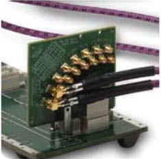
8 This image cannot currently be displayed. This image cannot currently be displayed. Measurement Equipment The last thing you want is your measurement equipment to collude against you as well! You need confidence you have : --Right tools for the job --Right setup --Right connection --Right Expectation

9 The Objective: Support Specified Link BER Data Bit Error Ratio is the key metric Probability that a bit is received in error. Link Model (Tx, Channel, Rx) Transmitter Channel Receiver + Tx - Emp Txp Txn Cnctr Channel Cnctr Rxp Rxn EQ + Rx -


10 Evaluating Portions of the System Transmitter + Tx - Emp Txp Txn Cnctr Channel Cnctr Channel Cnctr Receiver Cnctr Rxp Rxn EQ + Rx -


11 Receiver Testing Jitter Components (RJ+DJ+ISI) N4903B JBERT RJ+DJ+ISI Frame Error Rec Rx Tx Loop Back Device Under Chip Test RJ DJ ISI

12 Source Testing + Tx - Emp Txp Txn Cnctr Voltage Level Eye Diagram Jitter and the components of jitter Skew Pre-Emphasis/De-Emphasis Frequency/Data Rate Spread Spectrum Clocking parameters
13 Jitter Components Total Jitter (TJ) Bounded UnBounded Deterministic Jitter (DJ) Random Jitter (RJ) Correlated with Data (DDJ) Uncorrelated with Data (BUJ) DutyCycle Distortion (DCD) InterSymbol Interference (ISI) Non Periodic (ABUJ) Periodic (PJ) Gaussians ( RJ RMS ) Tr, Tf Settling Time Xtalk Clocks Thermal Reflections Non flat Freq Response Non Linear CR Events Xtalk Shot 1/f Burst


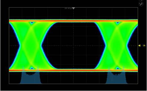
14 Jitter measurements on the same DUT performed by two different instruments Sampling Scope Real Time Scope A seemingly simple jitter measurement on a 10 Gbps device Why can the results be so different?

15 Sampling vs Real-time Oscilloscopes Topologies, Pros and Cons Equivalent-time Sampling Oscilloscope Real Time Oscilloscope
16 Equivalent-Time Sampling Extremely wide bandwidths at low sample rates 2 4-1=15 bits 2 4-1=15 bits PRBS Pattern Trigger Trigger Point Sampling Point Sequential Delay Reconstructed Waveform A sample is taken, the data pattern repeats and the next sample is taken at a slight delay compared to the previous sample In practice, samples are very close together (can be less than 100 fs apart). Through multiple passes of the signal, the waveform can be precisely reconstructed
 Sampler control pulse Since only one sample is taken, the A-D process can be very high resolution (up to 15 bits) with very low noise Sampler pulse: Low bandwidth")
17 Sampling Scope Bandwidth is Independent of Sample Rate S Sampler input Measurement bandwidth is affected by how narrow the sampler control pulse is (can be just a few picoseconds) Sampler control pulse Since only one sample is taken, the A-D process can be very high resolution (up to 15 bits) with very low noise Sampler pulse: Low bandwidth High bandwidth

18 Eye Diagrams: Highly Synchronous Sampling at Arbitrary Bit Locations PRBS Re-Arm Time Trigger Point Sampling Point Clock Trigger Reconstructed Waveform One Bit MYTH!: Sampling scopes can only display repetitive signals
19 Real-time Sampling Sample entire waveform in one acquisition S(t) T T Trigger Event T=1/F S Could Trigger Here. Or Here Nyquist criterion obeyed: Fs > 2*BW of signal Interpolation is used to precisely fill in points in between actual sampled points to yield better resolution
20 Oscilloscope Block Diagram Comparison 8bits Real Time Oscilloscope 16 bits Sampling Oscilloscope

21 Platform Pros and Cons Sampling Oscilloscope Bandwidth to > 90 GHz Lowest noise & jitter High precision long term view Precision optical receivers Price Real Time Oscilloscope Bandwidths to 63 GHz Sample rates up to 160 GSa/s High resolution short term capture Rich and flexible triggering Complete signal access (probing)
22 Jitter Measurements Same DUT Performed/Two Different Instruments Sampling Scope Real Time Scope A seemingly simple jitter measurement on a 10 Gbps device why can the results be so different?


23 What Causes Different Jitter Results? Clock Recovery Noise / Slew Rate Memory Depth Frequency Response Crosstalk Other issues to consider: 1. Jitter Thresholds (DCD) 2. Input Match (AC or DC coupled signal?) 23 S800 JITR_12_1 Labs.pptx January 28, 2013

24 Clock Recovery If you re not using equivalent clock recovery models, correlating jitter results will be VERY difficult. 24
 order, bandwidth, peaking, or damping factor")
 Data relative to a clean clock (narrow loop BW) OR Data relative to")
 indicates how much of the jitter on the input signal is transferred to the")
 j ( s) Jitter Multiplier 1.2 1 0.8 0.6 0.4 0.")
 0 1.0E+3 10.0E+3 100.0E+3 1.0E+6 10.0E+6 100.")
 high frequency jitter on the data stream is transferred to the receiver (HPF) OJTF")
 describe PLL requirements differently.")
25 Quick Review - Clock Recovery (CR) Basics o o o Provides a recovered clock for receiver Manages jitter in the system Standards specify CR Phase Locked Loop (PLL) order, bandwidth, peaking, or damping factor Input Signal Data Input Phase Detector Phase Error Amplifier Voltage Controlled Oscillator (VCO) Recovered Clock Sampler (Receiver) Data relative to a clean clock (narrow loop BW) OR Data relative to recovered clock (wide loop BW) Basic CR Block Diagram Narrow CR Loop BW OR Wide CR Loop BW PLL Jitter Transfer Function (JTF) indicates how much of the jitter on the input signal is transferred to the recovered clock (output) low-pass filter function (LPF) JTF Closed loop gain out A( s) G( s) G( s) e in 1 A( s) j ( s) Jitter Multiplier Clock Recovery PLL Response Jitter Transfer Function (JTF) and Observed Jitter Transfer Function (OJTF) 0 1.0E E E+3 1.0E E E+6 Frequency (Hz) Observed Jitter Transfer Function (OJTF) indicates the jitter that is observed by the receiver (scope) high frequency jitter on the data stream is transferred to the receiver (HPF) OJTF 1 JTF 1-G( s) 1 G( s) e j ( s) BEWARE of Clock Recovery (PLL) Definitions! Standards (and scopes) describe PLL requirements differently. Agilent 86100C/D Sampling Scope CR loop BW setting configures JTF JTF Example: Ethernet, SONET/SDH Agilent 90K Series Real-time Scope CR loop BW setting configures OJTF OJTF : SATA/SAS


26 Jitter Spectrum To understand how the CR PLL response impacts low frequency jitter, it is useful to observe jitter in the frequency domain Magnitude Frequency Offset frequency
 Jitter floor (without tones) is random jitter Observe all incoming jitter Track out low frequency jitter Clock Recovery response greatly impacts amount of jitter seen by receiver,")
27 Jitter Spectrum Shows distribution of low frequency jitter and impact of clock recovery Narrow CR loop bandwidth Wide CR loop bandwidth Spectral lines indicate deterministic jitter (including SSC and its odd harmonics) Jitter floor (without tones) is random jitter Observe all incoming jitter Track out low frequency jitter Clock Recovery response greatly impacts amount of jitter seen by receiver, and/or measured by an oscilloscope!


28 Clock Recovery Models 1 st Order PLL: JTF BW = OJTF BW Peaking/DF = none Roll-Off: 20 db/decade - Less ability to track out low frequency jitter and stay locked - Real hardware CR does not behave this way HW CR Loop Response Jitter Spectrum 2 nd Order, Type 2 PLL: Bandwidth: JTF BW > OJTF BW Peaking/Damping Factor: need to specify Roll-Off: 40 db/decade (tracks out low jitter more than 1 st order PLL) HW CR response may have higher peaking in OJTF than desired. This will amplify jitter in this region. Note significance depends on DUT jitter spectrum. 3 rd Order PLL: JTF BW > OJTF BW - Specify zero, gain, pole frequencies. - Roll-Off: 60 db/decade below zero frequency - Use PLL Response Tutorial workbook to model. Desired SW CR Loop Response e.g. match a standard exactly Jitter Spectrum Less Peaking 86108B FTD_DCA_224 Agilent Restricted March 2012

 Integrated Hardware Clock Recovery Filtered")


29 Jitter Spectrum Analysis and SW Clock Recovery Emulation using Agilent 86100D/86108B-JSA 86108A/B Module Device Under Test Data or Clock Signal ( Jitter Filter ) Integrated Hardware Clock Recovery Filtered Signal ( Jitter Fitler ) Ideal Software Clock Recovery Emulation Real CR PLL response Adjustable Loop Bandwidth Adjustable Peaking (discrete) Ideal, flexible CR PLL response Adjustable Loop Bandwidth Adjustable Peaking (continuous) Desired SW CR Loop Response e.g. match a standard exactly Less Peaking HW CR response may have higher peaking in OJTF than desired. Jitter amplification will occur in region where unwanted peaking exists. Jitter Spectrum Apply ideal PLL using Software Clock Recovery Emulation Jitter Spectrum Note how much of an increase depends on DUT jitter spectrum. Higher Accuracy Hardware only clock recovery Ideal SW Clock Recovery Model


30 Clock Recovery Comparison Always use similar clock recovery models Apples-to-Apples setup Agilent K X-Series X-Series Agilent 86100D with 86108B 30
 Agilent 90K X-Series CR BW: 10 MHz (OJTF) Not an apples-apples")
31 10 Gb/s Jitter Measurement Demo Part 1 Perform a jitter measurement using 10 MHz CR loop bandwidth. 10G Pattern Generator D+ D- Agilent 86100D CR BW: 10 MHz (JTF) Agilent 90K X-Series CR BW: 10 MHz (OJTF) Not an apples-apples measurement with respect to clock recovery!


32 10 Gb/s Jitter Measurement Demo Part 2 Perform a jitter measurement using 2 nd Order CR response with 10MHz OJTF and DF. 10G Pattern Generator D+ D- JTF: 2 nd Order, 20 MHz Loop BW, 2dB Peaking OJTF: 2 nd Order 10 MHz Loop BW, DF OJTF: 2 nd Order 10 MHz Loop BW, DF We are using the same CR setup now, but are there other things we should look at?

 PLL+DCA out ( s) ( s) Peak is reduced from ~1.4 down to ~ 1.")
 24 ns delay 0 ns delay Delay data signal using specially")
33 Clock Recovery: Clock-to-Data Trigger Delay Clock-to-Data Trigger delay adds phase shifts Effect on OJTF => peaking (amplifies jitter!) Introduced when using External Clock Recovery JTF (BERT, Sampling Scopes, Explicit Clocks ) PLL+DCA out ( s) ( s) Peak is reduced from ~1.4 down to ~ 1.1 by decreasing the effective trigger delay in. e -j (trigger delay) 24 ns delay 0 ns delay Delay data signal using specially matched cables (see vendo (degrades signal integrity, however)
 Agilent 90K")
 Note - single-ended noise measurements since we re")
34 Oscilloscope Noise Impacts Measured Jitter - Demo Measure AC rms measurement at proper Volts/Div scale for DUT signal Agilent 86100D/86108B Series: ~ 640 uv (at 35 GHz BW Setting) Agilent 90K X-Series: ~ 6.1 mv (at 137 mv/div and 32 GHz BW Setting) Note - single-ended noise measurements since we re performing a comparison using singleended signals (analyzing P and N from the same DUT)

35 Manually Determine Induced Jitter due to Scope Noise and Signal s Slew Rate RN = Random Noise(rms) Slew Rate = rate of change of signal in V / ns = Delta V/ Delta T Induced Jitter due to scope noise: D / 86108B DCA-X Noise = 640 uv Slew Rate = mv / 8.34 ps = 20.8 V/ns Induced Jitter = RN / SlewRate = 640uV / 20.8V/ns Induced Jitter = 31 fs Delta T Delta V 2. 90K X-Series Oscilloscope Noise = 6.1 mv Slew Rate = 26 V/ns Induced Jitter = RN /SlewRate = 6.1mV / 26 V/ns Induced Jitter = 234 fs The faster the edge, the smaller the problem! And vice-versa!
36 Estimate Jitter due to Intrinsic Scope Jitter/Noise and Signal s Slew Rate (AM-to-PM Conversion) Example: 86100D / 86108B 1. DUT Random Jitter = 200 fs 2. Scope Random Jitter = 50 fs Random Timing Jitter = 206 fs = SQRT [(200^2)+(50^2)] 3. Noise Induced Jitter from scope = 31 fs (see previous page) Example: 90K X-Series 1. DUT Random Jitter = 200 fs 2. Scope Random Jitter = 75 fs Random Timing Jitter = 213 fs = SQRT [(200^2)+(75^2)] 3. Noise Induced Jitter from scope = 234 fs (see previous page) Measured Jitter = SQRT [(Timing Jitter)^2 + (AM-to-PM Jitter)^2)] Measured Jitter = SQRT [(206)^2 + (31)^2)] = 208 fs Measured Jitter = SQRT [(213)^2 + (234)^2)] = 317 fs Scope jitter results include noise induced jitter (AM-to-PM conversion). Results change due to signal slew rate and random noise.


37 Use FlexDCA simulator to determine induced jitter due to noise/slew rate on saved waveforms Actual saved waveform => Playback and add 640 uv rms random noise Add Noise Only Add Jitter + Noise DCA 35GHz BW, 50 mv/div RJ due to scope noise only. RJ due to timing jitter and scope noise. Minimize scope BW to reduce noise, especially if signal has slow edges!
38 Summary - Noise / Slew Rate As random noise (RN) increases, random jitter increases. Especially problematic with slower edge speeds! Minimize oscilloscope noise. Use only enough BW to capture signal. 38 S800 JITR_12_1 Labs.pptx January 28, 2013


 vs Wide (white) White Paper")

39 Memory Depth and Wide vs Narrow Mode (RT Scope settings) Pay attention to the BER Bathtub plots! RJ vs Memory Depth: White Paper: (see page 35-37). Increase memory depth until RJ result stabilizes Check BER Bathtub curves to ensure a continuous function RJ Bandwidth: Narrow (pink) vs Wide (white) White Paper Start with narrow RJ setting Discontinuities in the BER Bathtub graph should be a red flag! 39 S800 JITR_12_1 Labs.pptx January 28, 2013


40 Receiver Frequency Response Differences in scope receiver s frequency response will change: Shape of eye diagram Amplitude Rise/fall times ISI 40 S800 JITR_12_1 Labs.pptx January 28, 2013


41 Frequency Response Step Response What does each filter response look like and do to a step? 33 GHz Sinc 50 GHz Sinc Filter Waveform: 10 GHz/div, 3 db/div Step Waveform: 100 ps/div Yellow frequency response Blue step response 50 GHz Flat Real-time Scope 50 GHz Bessel Real-time Scope Closest to Sampling Scope RX


42 Frequency Response 50 GHz BW 28 Gb/s eye with infinite TX bandwidth 86108B 50 GHz Raw Corrected to 50 GHz Sinc Which eye amplitude is higher? Answer: They re about the same. Corrected to 50 GHz Flat Corrected to 50 GHz Bessel


 Corrected to 33 GHz Flat Corrected to 33 GHz Bessel RX")
43 Frequency Response 33 GHz 28 Gb/s eye with infinite TX bandwidth 86108B 50 GHz Raw Corrected to 33 GHz Sinc Same input signal which eye amplitude is higher now? Answer: 33GHz Sinc, even though it has less BW (more energy above the mean 1 level.) Corrected to 33 GHz Flat Corrected to 33 GHz Bessel RX Frequency Response: Amplitude and Phase response are important.


44 Frequency Response Use FFT to determine how much BW to use 10Gbps signal measured using different BW on a RT Scope 32 GHz GHz 20 GHz 15GHz To ensure optimal waveform accuracy, use sufficient BW to capture all energy in the signal, but only use what you need to minimize noise.


45 Frequency Response 63 GHz Sinc Simulated 28G, 37 GHz 4 th Order Bessel 50 GHz Sinc 33 GHz Sinc Simulated Recommend using more than 33GHz BW for this 28Gb/s signal! 86108B 50 GHz Simulated 45 S800 JITR_12_1 Labs.pptx January 28, 2013
46 Agilent Application Software Take all the guess work out of setting up a scope for an accurate, and compliant, measurement D DCA-X N1012A CEI 3.0 6G/11G/25G/28G and 28G VSR (Draft) N1019A SFF-8431 (10G SFP+) N1019A User-Defined Application X-Series, Q-Series Scopes DDR, DVI, DisplayPort, Ethernet, Fully Buffered DIMM, GDDR, HDMI, MHL, MIPI, PCI Express, Secure Digital, Serial ATA I/II, Thunderbolt, USB, Wireless USB, XAUI, and more!

47 Agilent Application Software - Thunderbolt Demo TBT Application using TBT as DUT


48 DEMO Spectral RJ Extraction Tail Fit RJ Extraction
 DutyCycle Distortion (DCD) InterSymbol Interference (ISI) Uncorrelated with Data (BUJ) Non Periodic (ABUJ) Periodic (PJ) The problem with crosstalk jitter arises from")
49 Crosstalk Bounded Jitter that is Deterministic and is uncorrelated with the Data may be Periodic or Aperiodic. Deterministic Jitter (DJ) Periodic is easily identified, Aperiodic jitter is not. Correlated with Data (DDJ) DutyCycle Distortion (DCD) InterSymbol Interference (ISI) Uncorrelated with Data (BUJ) Non Periodic (ABUJ) Periodic (PJ) The problem with crosstalk jitter arises from techniques to separate jitter into its constituent components Tr, Tf Settling Time Xtalk Clocks Reflections Non flat Freq Response Non Linear CR Events Xtalk Aggressor


50 Crosstalk cont The problem with crosstalk jitter arises from techniques to separate jitter into its constituent components ISI PJ By examining repetitions of the pattern you can definitively identify the ISI and remove it from the T.I.E record. RJ DJ ISI What remains is PJ and RJ and an easy way to separate them through spectral analysis---because periodic components are easily identified in the frequency domain RJ RJ time error likely to contain PJ PJ threshold 0 0 freq

 will make the RJ look bigger time")
51 Crosstalk (2) But what if crosstalk IS present? You can still remove the Data Dependent Jitter, but the PJ/RJ separation wont work because the spectrum of crosstalk MOST likely is NOISE LIKE. Therefore, Crosstalk (or Aperiodic Bounded Uncorrelated Jitter) will make the RJ look bigger time error likely to contain PJ RJ DJ ISI PJ threshold 0 0 freq You need to have a Gaussian Tailfit Extraction for the RJ


52 RJ Extraction with Crosstalk (ABUJ) Spectral vs. Gaussian RJ Extraction. No Crosstalk w/crosstalk X Spectral Extraction Examine slope continuity Spectral Extraction Compare actual Data with RJ estimates of both methods Gaussian Tailfit Extraction Gaussian Tailfit Extraction

53 Two Ways to Analyze ABUJ 1. Use Gaussian Tailfit Extraction 2. Two Pass Spectral Extraction Approach assumes you have control of the interferer assumes conveyed jitter of interferer is all BUJ 1.47 ps


54 ABUJ/Crosstalk Analysis 1. Gaussian Tailfit Extraction No interferer With interferer Victim Aggressor Aggressor at transition
55 ABUJ/Crosstalk Analysis 2. Two Pass approach a) Turn off crosstalk element(s). b) Measure jitter (jitter components) c) Turn on crosstalk element(s) d) Enter RJ rms value for RJ ( specify ) e) Crosstalk (ABUJ) will go into bounded portion of jitter which will prevent overestimation of RJ and Total Jitter ps


56 ABUJ/Crosstalk Analysis Two Pass Approach No interferer With interferer Victim Aggressor Aggressor at transition

 Compliance packages can off load engineer from being an expert Don t be the mule! Offload it!")
57 Summary The engineer facing high speed problems is facing an uphill climb SI Problems Takes some effort to get correlation between real time scopes and sampling scopes. (Clock Recovery, frequency response, noise, etc.) Compliance packages can off load engineer from being an expert Don t be the mule! Offload it! Crosstalk may be present and if you suspect it, then it is helpful to have a couple of ways to understand its effects
High Speed Digital Design & Verification Seminar. Measurement fundamentals
 High Speed Digital Design & Verification Seminar Measurement fundamentals Agenda Sources of Jitter, how to measure and why Importance of Noise Select the right probes! Capture the eye diagram Why measure
Real Time Jitter Analysis
 Real Time Jitter Analysis Agenda ı Background on jitter measurements Definition Measurement types: parametric, graphical ı Jitter noise floor ı Statistical analysis of jitter Jitter structure Jitter PDF
Jitter Measurements using Phase Noise Techniques
 Jitter Measurements using Phase Noise Techniques Agenda Jitter Review Time-Domain and Frequency-Domain Jitter Measurements Phase Noise Concept and Measurement Techniques Deriving Random and Deterministic
DesignCon Analysis of Crosstalk Effects on Jitter in Transceivers. Daniel Chow, Altera Corporation
 DesignCon 2008 Analysis of Crosstalk Effects on Jitter in Transceivers Daniel Chow, Altera Corporation dchow@altera.com Abstract As data rates increase, crosstalk becomes an increasingly important issue.
Jitter analysis with the R&S RTO oscilloscope
 Jitter analysis with the R&S RTO oscilloscope Jitter can significantly impair digital systems and must therefore be analyzed and characterized in detail. The R&S RTO oscilloscope in combination with the
Jitter in Digital Communication Systems, Part 1
 Application Note: HFAN-4.0.3 Rev.; 04/08 Jitter in Digital Communication Systems, Part [Some parts of this application note first appeared in Electronic Engineering Times on August 27, 200, Issue 8.] AVAILABLE
Analysis and Decomposition of Duty Cycle Distortion from Multiple Sources
 DesignCon 2013 Analysis and Decomposition of Duty Cycle Distortion from Multiple Sources Daniel Chow, Ph.D., Altera Corporation dchow@altera.com Shufang Tian, Altera Corporation stian@altera.com Yanjing
Operation Guide: Using the 86100C DCA-J Jitter Spectrum and Phase Noise Application Revision 1.0
 Operation Guide: Using the 86100C DCA-J Jitter Spectrum and Phase Noise Application Revision 1.0 I Overview The Jitter Spectrum and Phase Noise (JSPN) Application is based on a Microsoft Excel spreadsheet
MIPI S-parameter & Impedance Measurements with ENA Option TDR. Last update: 2014/04/08 (HK)
") MIPI S-parameter & Impedance Measurements with ENA Option TDR Last update: 2014/04/08 (HK) 1 MIPI Interfaces in a Mobile Platform 2 MIPI High Speed Physical, Protocol & App Layer Application Protocol Standard
MIPI S-parameter & Impedance Measurements with ENA Option TDR Last update: 2014/04/08 (HK) 1 MIPI Interfaces in a Mobile Platform 2 MIPI High Speed Physical, Protocol & App Layer Application Protocol Standard
Picking the Optimal Oscilloscope for Serial Data Signal Integrity Validation and Debug
 Picking the Optimal Oscilloscope for Serial Data Signal Integrity Validation and Debug Application Note 1556 Introduction In the past, it was easy to decide whether to use a real-time oscilloscope or an
Student Research & Creative Works
 Scholars' Mine Masters Theses Student Research & Creative Works Summer 216 Study jitter amplification of a passive channel and investigation of S 21 magnitude extraction methodologies using a pattern generator
Jitter Analysis Techniques Using an Agilent Infiniium Oscilloscope
 Jitter Analysis Techniques Using an Agilent Infiniium Oscilloscope Product Note Table of Contents Introduction........................ 1 Jitter Fundamentals................. 1 Jitter Measurement Techniques......
ECEN620: Network Theory Broadband Circuit Design Fall 2014
 ECEN620: Network Theory Broadband Circuit Design Fall 2014 Lecture 16: CDRs Sam Palermo Analog & Mixed-Signal Center Texas A&M University Announcements Project descriptions are posted on the website Preliminary
Keysight Technologies EZJIT Complete Jitter and Vertical Noise Analysis Software for Infiniium Oscilloscopes. Data Sheet
 Keysight Technologies EZJIT Complete Jitter and Vertical Noise Analysis Software for Infiniium Oscilloscopes Data Sheet 02 Keysight EZJIT Complete Jitter and Vertical Noise Analysis Software for Infiniium
Agilent Technologies High-Definition Multimedia
 Agilent Technologies High-Definition Multimedia Interface (HDMI) Cable Assembly Compliance Test Test Solution Overview Using the Agilent E5071C ENA Option TDR Last Update 013/08/1 (TH) Purpose This slide
Introduction to Jitter Techniques for High Speed Serial Technologies
 Introduction to Jitter Techniques for High Speed Serial Technologies Industry Trends Fast Data Rates, More HF Loss Clean, open, logical 1 & 0 at launch from transmitter Logical 1 & 0 can be hard to distinguish
Keysight Technologies J-BERT M8020A High-Performance BERT
 Keysight Technologies J-BERT M8020A High-Performance BERT Data Sheet Version 3.5 NEW Interactive Link Training for USB 3.0 and USB 3.1 Interactive Link Training for PCI Epress 8 GT/s and 16 GT/s TX Equalizer
Keysight Technologies Precision Jitter Analysis Using the Keysight 86100C DCA-J. Application Note
 Keysight Technologies Precision Jitter Analysis Using the Keysight 86100C DCA-J Application Note Introduction The extremely wide bandwidth of equivalent-time sampling oscilloscopes makes them the tool
SV2C 28 Gbps, 8 Lane SerDes Tester
 SV2C 28 Gbps, 8 Lane SerDes Tester Data Sheet SV2C Personalized SerDes Tester Data Sheet Revision: 1.0 2015-03-19 Revision Revision History Date 1.0 Document release. March 19, 2015 The information in
Agilent J-BERT N4903A High-Performance Serial BERT with Complete Jitter Tolerance Testing 7 Gb/s and 12.5 Gb/s
 Agilent J-BERT N4903A High-Performance Serial BERT with Complete Jitter Tolerance Testing 7 Gb/s and 12.5 Gb/s Version 3.1 New: Fastest Jitter Tolerance Results (SW 4.5) New: Pattern Generator (options
EBERT 2904 Pulse Pattern Generator and Error Detector Datasheet
 EBERT 2904 Pulse Pattern Generator and Error Detector Datasheet REV 1.0 2904 KEY FEATURES Four channel NRZ Pulse Pattern Generator and Error Detector Operating range between 24.6 to 29.5 Gb/s along with
Bridging the Measurement and Simulation Gap Sarah Boen Marketing Manager Tektronix
 Bridging the Measurement and Simulation Gap Sarah Boen Marketing Manager Tektronix 1 Agenda Synergy between simulation and lab based measurements IBIS-AMI overview Simulation and measurement correlation
EBERT 1504 Pulse Pattern Generator and Error Detector Datasheet
 EBERT 1504 Pulse Pattern Generator and Error Detector Datasheet REV 1.0 1504 KEY FEATURES Four channel NRZ Pulse Pattern Generator and Error Detector Wide operating range between 1 to 15 Gb/s and beyond
Date: October 4, 2004 T10 Technical Committee From: Bill Ham Subject: SAS 1.1 PHY jitter MJSQ modifications
 SAS 1.1 PHY jitter MJSQ modifications T10/04-332r0 Date: October 4, 2004 To: T10 Technical Committee From: Bill Ham (bill.ham@hp,com) Subject: SAS 1.1 PHY jitter MJSQ modifications The following proposed
Jitter Fundamentals: Jitter Tolerance Testing with Agilent ParBERT. Application Note. Introduction
 Jitter Fundamentals: Jitter Tolerance Testing with Agilent 81250 ParBERT Application Note Introduction This document allows designers of medium complex digital chips to gain fast and efficient insight
Configuring the MAX3861 AGC Amp as an SFP Limiting Amplifier with RSSI
 Design Note: HFDN-22. Rev.1; 4/8 Configuring the MAX3861 AGC Amp as an SFP Limiting Amplifier with RSSI AVAILABLE Configuring the MAX3861 AGC Amp as an SFP Limiting Amplifier with RSSI 1 Introduction As
Agilent EEsof EDA.
 Agilent EEsof EDA This document is owned by Agilent Technologies, but is no longer kept current and may contain obsolete or inaccurate references. We regret any inconvenience this may cause. For the latest
UFS v2.0 PHY and Protocol Testing for Compliance. Copyright 2013 Chris Loberg, Tektronix
 UFS v2.0 PHY and Protocol Testing for Compliance Copyright 2013 Chris Loberg, Tektronix Agenda Introduction to MIPI Architecture & Linkage to UFS Compliance Testing Ecosystem UFS Testing Challenges Preparing
40 AND 100 GIGABIT ETHERNET CONSORTIUM
 40 AND 100 GIGABIT ETHERNET CONSORTIUM Clause 93 100GBASE-KR4 PMD Test Suite Version 1.0 Technical Document Last Updated: October 2, 2014 40 and 100 Gigabit Ethernet Consortium 121 Technology Drive, Suite
Characterizing High-Speed Oscilloscope Distortion A comparison of Agilent and Tektronix high-speed, real-time oscilloscopes
 Characterizing High-Speed Oscilloscope Distortion A comparison of Agilent and Tektronix high-speed, real-time oscilloscopes Application Note 1493 Table of Contents Introduction........................
Clock Recovery Instrument
 Clock Recovery Instrument BERTScope CR Series Datasheet Built-in Equalizer Function enables Clock Recovery under High ISI Input Conditions Data Measurement Capability Edge Density Measurement Determine
Limitations And Accuracies Of Time And Frequency Domain Analysis Of Physical Layer Devices
 Limitations And Accuracies Of Time And Frequency Domain Analysis Of Physical Layer Devices Outline Short Overview Fundamental Differences between TDR & Instruments Calibration & Normalization Measurement
An Introduction to Jitter Analysis. WAVECREST Feb 1,
 An Introduction to Jitter Analysis WAVECREST Feb 1, 2000 1 Traditional View Of Jitter WAVECREST Feb 1, 2000 2 Jitter - What is Jitter? The deviation from the ideal timing of an event. The reference event
06-011r0 Towards a SAS-2 Physical Layer Specification. Kevin Witt 11/30/2005
 06-011r0 Towards a SAS-2 Physical Layer Specification Kevin Witt 11/30/2005 Physical Layer Working Group Goal Draft a Specification which will: 1. Meet the System Designers application requirements, 2.
Keysight Technologies Greg LeCheminant / Robert Sleigh
 Keysight Technologies 2018.01.31 Greg LeCheminant / Robert Sleigh Introduction Why use Pulse Amplitude Modulation 4-Level (PAM4)? Review Standards using PAM4 Output (Transmitter) Characterization Key Optical
High-Throughput, High- Sensitivity Measurement of Power Supply-Induced Bounded, Uncorrelated Jitter in Time, Frequency, and Statistical Domains
 DesignCon 2013 High-Throughput, High- Sensitivity Measurement of Power Supply-Induced Bounded, Uncorrelated Jitter in Time, Frequency, and Statistical Domains Daniel Chow, Ph.D., Altera Corporation dchow@altera.com
Beta and Epsilon Point Update. Adam Healey Mark Marlett August 8, 2007
 Beta and Epsilon Point Update Adam Healey Mark Marlett August 8, 2007 Contributors and Supporters Dean Wallace, QLogic Pravin Patel, IBM Eric Kvamme, LSI Tae-Kwang Jeon, LSI Bill Fulmer, LSI Max Olsen,
Clock Recovery Instrument BERTScope CR Series Datasheet
 Clock Recovery Instrument BERTScope CR Series Datasheet Key features Instrumentation quality clock recovery Accurate, variable loop bandwidth from 100 khz to 12 MHz, with optional 24 MHz for the jitter
ECEN720: High-Speed Links Circuits and Systems Spring 2017
 ECEN720: High-Speed Links Circuits and Systems Spring 2017 Lecture 12: CDRs Sam Palermo Analog & Mixed-Signal Center Texas A&M University Announcements Project Preliminary Report #2 due Apr. 20 Expand
M.2 SSIC SM Electrical Test Specification Version 1.0, Revision 0.5. August 27, 2013
 M.2 SSIC SM Electrical Test Specification Version 1.0, Revision 0.5 August 27, 2013 Revision Revision History DATE 0.5 Preliminary release 8/23/2013 Intellectual Property Disclaimer THIS SPECIFICATION
All About the Acronyms: RJ, DJ, DDJ, ISI, DCD, PJ, SJ, Ransom Stephens, Ph.D.
 All About the Acronyms: RJ, DJ, DDJ, ISI, DCD, PJ, SJ, Ransom Stephens, Ph.D. Abstract: Jitter analysis is yet another field of engineering that is pock-marked with acronyms. Each category and type of
Characterization and Compliance Testing for 400G/PAM4 Designs. Project Manager / Keysight Technologies
 Characterization and Compliance Testing for 400G/PAM4 Designs Project Manager / Keysight Technologies Jacky Yu & Gary Hsiao 2018.06.11 Taipei State of the Standards (Jacky Yu) Tx test updates and learnings
Table 1: Cross Reference of Applicable Products
 Standard Product UT7R995/C RadClock Jitter Performance Application Note January 21, 2016 The most important thing we build is trust Table 1: Cross Reference of Applicable Products PRODUCT NAME RadClock
Basic Communication Laboratory Manual. Shimshon Levy&Harael Mualem
 Basic Communication Laboratory Manual Shimshon Levy&Harael Mualem September 2006 CONTENTS 1 The oscilloscope 2 1.1 Objectives... 2 1.2 Prelab... 2 1.3 Background Theory- Analog Oscilloscope...... 3 1.4
10GBASE-T Transmitter SNDR Definition (System ID Approach) IEEE P802.3an Task Force Santa Clara, Feb 2005 Albert Vareljian, Hiroshi Takatori KeyEye
 IEEE P802.3an Task Force Santa Clara, Feb 2005 Albert Vareljian, Hiroshi Takatori KeyEye") 10GBASE-T Transmitter SNDR Definition (System ID Approach) IEEE P802.3an Task Force Santa Clara, Feb 2005 Albert Vareljian, Hiroshi Takatori KeyEye 1 OUTLINE Transmitter Performance Evaluation Block Diagram
10GBASE-T Transmitter SNDR Definition (System ID Approach) IEEE P802.3an Task Force Santa Clara, Feb 2005 Albert Vareljian, Hiroshi Takatori KeyEye 1 OUTLINE Transmitter Performance Evaluation Block Diagram
M8040A High-Performance BERT 64 Gbaud
 DATA SHEET M8040A High-Performance BERT 64 Gbaud Version 3.0 Master your next design New features: Integrated clock recovery PCI Express 5.0 support ISI channel boards Error distribution analysis Table
Advanced Memory Buffer (AMB), Characterization of Timing and Voltage Specifications
, Characterization of Timing and Voltage Specifications") Advanced Memory Buffer (AMB), Characterization of Timing and Voltage Specifications Application Note Introduction Higher CPU speeds drive the need for higher memory bandwidth. For decades, CPUs have connected
Advanced Memory Buffer (AMB), Characterization of Timing and Voltage Specifications Application Note Introduction Higher CPU speeds drive the need for higher memory bandwidth. For decades, CPUs have connected
SHF Communication Technologies AG. Wilhelm-von-Siemens-Str. 23D Berlin Germany. Phone Fax
 SHF Communication Technologies AG Wilhelm-von-Siemens-Str. 23D 12277 Berlin Germany Phone +49 30 772051-0 Fax ++49 30 7531078 E-Mail: sales@shf.de Web: http://www.shf.de Application Note Jitter Injection
06-496r3 SAS-2 Electrical Specification Proposal. Kevin Witt SAS-2 Phy Working Group 1/16/07
 06-496r3 SAS-2 Electrical Specification Proposal Kevin Witt SAS-2 Phy Working Group 1/16/07 Overview Motivation Multiple SAS-2 Test Chips Have Been Built and Tested, SAS-2 Product Designs have Started
Advanced Product Design & Test for High-Speed Digital Devices
 Advanced Product Design & Test for High-Speed Digital Devices Presenters Part 1-30 min. Hidekazu Manabe Application Marketing Engineer Agilent Technologies Part 2-20 min. Mike Engbretson Chief Technology
Agilent J-BERT N4903B High-performance Serial BERT
 Agilent J-BERT N4903B High-performance Serial BERT 7 Gb/s and 12.5 Gb/s Preliminary Data Sheet Version 0.9 Complete jitter tolerance test for embedded and forwarded clock devices Integrated Calibrated
Keysight Technologies M8062A 32 Gb/s Front-End for J-BERT M8020A High-Performance BERT
 Keysight Technologies M8062A 32 Gb/s Front-End for J-BERT M8020A High-Performance BERT Data Sheet Version 3.5 Introduction The M8062A extends the data rate of the J-BERT M8020A Bit Error Ratio Tester to
J-BERT M8020A High-Performance BERT
 DATA SHEET VERSION 5.0 J-BERT M8020A High-Performance BERT Master your net designs Table of Contents Introduction 3 Key features 3 Applications 3 M8000 Series of BER Test Solutions 4 J-BERT M8020A high-performance
Comparison and Correlation of Signal Integrity Measurement Techniques
 DesignCon 2002 High-Performance System Design Conference Comparison and Correlation of Signal Integrity Measurement Techniques John Patrin, Ph.D. Mike Li, Ph.D. Wavecrest 1 Abstract Data communication
F i n i s a r. Product Specification C.wire 120 Gb/s Parallel Active Optical Cable FCBGD10CD1Cxx
 Product Specification C.wire 120 Gb/s Parallel Active Optical Cable FCBGD10CD1Cxx PRODUCT FEATURES 12-channel full-duplex active optical cable Electrical interface only Multirate capability: 1.06Gb/s to
Agilent N5411A Serial ATA Electrical Performance Validation and Compliance Software Release Notes
 Agilent N5411A Serial ATA Electrical Performance Validation and Compliance Software Release Notes Agilent N5411A Software Version 2.60 Released Date: 7 Nov 2008 Minimum Infiniium Oscilloscope Baseline
IEEE 802.3ba 40Gb/s and 100Gb/s Ethernet Task Force 22th Sep 2009
 Draft Amendment to IEEE Std 0.-0 IEEE Draft P0.ba/D. IEEE 0.ba 0Gb/s and 00Gb/s Ethernet Task Force th Sep 0.. Stressed receiver sensitivity Stressed receiver sensitivity shall be within the limits given
Keysight Technologies BER Measurement Using a Real-Time Oscilloscope Controlled From M8070A. Application Note
 Keysight Technologies BER Measurement Using a Real-Time Oscilloscope Controlled From M8070A Application Note 02 Keysight BER Measurement Using Real-Time Oscilloscope Controlled from M8070A - Application
Latest Physical Layer test Methodologies in SATASAS 6G
 Latest Physical Layer test Methodologies in SATASAS 6G John Calvin Tektronix Storage Portfolio Product Manager Chairman of SATA-IO Logo and Interoperability Working group Presenter Biography John Calvin,
Channel operating margin for PAM4 CDAUI-8 chip-to-chip interfaces
 Channel operating margin for PAM4 CDAUI-8 chip-to-chip interfaces Adam Healey Avago Technologies IEEE P802.3bs 400 GbE Task Force March 2015 Introduction Channel Operating Margin (COM) is a figure of merit
Product Specification Quadwire FDR Parallel Active Optical Cable FCBN414QB1Cxx
 Product Specification Quadwire FDR Parallel Active Optical Cable FCBN414QB1Cxx PRODUCT FEATURES Four-channel full-duplex active optical cable Eletrical interface only Multirate capability: 1.06Gb/s to
Jitter Fundamentals: Agilent ParBERT Jitter Injection and Analysis Capabilities. Application Note. Jitter Fundamentals
 Jitter Fundamentals: Agilent 81250 ParBERT Jitter Injection and Analysis Capabilities Application Note Introduction In digital communications, a sequence of 0 s and 1 s flows from a transmitter to a receiver.
To learn statistical bit-error-rate (BER) simulation, BER link noise budgeting and using ADS to model high speed I/O link circuits
 simulation, BER link noise budgeting and using ADS to model high speed I/O link circuits") 1 ECEN 720 High-Speed Links: Circuits and Systems Lab6 Link Modeling with ADS Objective To learn statistical bit-error-rate (BER) simulation, BER link noise budgeting and using ADS to model high speed
1 ECEN 720 High-Speed Links: Circuits and Systems Lab6 Link Modeling with ADS Objective To learn statistical bit-error-rate (BER) simulation, BER link noise budgeting and using ADS to model high speed
SAS-2 6Gbps PHY Specification
 SAS-2 6Gbps PHY Specification T10/07-339r4 Date: September 6, 2007 To: T10 Technical Committee From: Alvin Cox (alvin.cox@seagate.com) Subject: SAS-2 6Gbps PHY Electrical Specification Abstract: The attached
M8195A 65 GSa/s Arbitrary Waveform Generator
 Arbitrary Waveform Generator New AWG with the highest combination of speed, bandwidth and channel density Juergen Beck Vice President & General Mgr. Digital & Photonic Test Division September 10, 2014
04-370r1 SAS-1.1 Merge IT and IR with XT and XR 1 December 2004
 To: T10 Technical Committee From: Rob Elliott, HP (elliott@hp.com) Date: 1 December 2004 Subject: 04-370r1 SAS-1.1 Merge and with XT and XR Revision history Revision 0 (6 November 2004) First revision
Understanding Apparent Increasing Random Jitter with Increasing PRBS Test Pattern Lengths
 JANUARY 28-31, 2013 SANTA CLARA CONVENTION CENTER Understanding Apparent Increasing Random Jitter with Increasing PRBS Test Pattern Lengths 9-WP6 Dr. Martin Miller The Trend and the Concern The demand
TITLE. Capturing (LP)DDR4 Interface PSIJ and RJ Performance. Image. Topic: Topic: John Ellis, Synopsys, Inc. Topic: malesuada blandit euismod.
DDR4 Interface PSIJ and RJ Performance. Image. Topic: Topic: John Ellis, Synopsys, Inc. Topic: malesuada blandit euismod.") TITLE Topic: o Nam elementum commodo mattis. Pellentesque Capturing (LP)DDR4 Interface PSIJ and RJ Performance malesuada blandit euismod. Topic: John Ellis, Synopsys, Inc. o o Nam elementum commodo mattis.
TITLE Topic: o Nam elementum commodo mattis. Pellentesque Capturing (LP)DDR4 Interface PSIJ and RJ Performance malesuada blandit euismod. Topic: John Ellis, Synopsys, Inc. o o Nam elementum commodo mattis.
SV3C CPTX MIPI C-PHY Generator. Data Sheet
 SV3C CPTX MIPI C-PHY Generator Data Sheet Table of Contents Table of Contents Table of Contents... 1 List of Figures... 2 List of Tables... 2 Introduction... 3 Overview... 3 Key Benefits... 3 Applications...
Validation & Analysis of Complex Serial Bus Link Models
 Validation & Analysis of Complex Serial Bus Link Models Version 1.0 John Pickerd, Tektronix, Inc John.J.Pickerd@Tek.com 503-627-5122 Kan Tan, Tektronix, Inc Kan.Tan@Tektronix.com 503-627-2049 Abstract
SHF Communication Technologies AG
 SHF Communication Technologies AG Wilhelm-von-Siemens-Str. 23D 12277 Berlin Germany Phone +49 30 772051-0 Fax +49 30 7531078 E-Mail: sales@shf.de Web: http://www.shf.de Datasheet SHF 78120 D Synthesized
ValiFrame N5990A MIPI M-PHY Transmitter Test
 ValiFrame N5990A MIPI M-PHY Transmitter Test Method of Implementation The ValiFrame Test Automation software provides physical testing of MIPI M-PHY devices with test instruments listed in 1. The tests
Agilent J-BERT N4903B High-Performance Serial BERT. Complete jitter tolerance test for embedded and forwarded clock devices
 Agilent J-BERT N4903B High-Performance Serial BERT 7 Gb/s and 12.5 Gb/s Data Sheet Version 1.3 (PCIe3.0 SKPOS fi ltering and calibration channels, support of 32 Gb/s clock data recovery with demultiplexer
Getting the most out of your Measurements Workshop. Mike Schnecker
 Getting the most out of your Measurements Workshop Mike Schnecker Agenda Oscilloscope Basics Using a RTE1000 Series Oscilloscope. Probing Basics Passive probe compensation Ground lead effects Vertical
Dual-Rate Fibre Channel Repeaters
 9-292; Rev ; 7/04 Dual-Rate Fibre Channel Repeaters General Description The are dual-rate (.0625Gbps and 2.25Gbps) fibre channel repeaters. They are optimized for use in fibre channel arbitrated loop applications
SiTime University Turbo Seminar Series
 SiTime University Turbo Seminar Series How to Measure Clock Jitter Part I Principle and Practice April 8-9, 2013 Agenda Jitter definitions and terminology Who cares about jitter How to measure clock jitter
High-speed Serial Interface
 High-speed Serial Interface Lect. 9 Noises 1 Block diagram Where are we today? Serializer Tx Driver Channel Rx Equalizer Sampler Deserializer PLL Clock Recovery Tx Rx 2 Sampling in Rx Interface applications
Bit Error Rate Tester BERTScope BSA Series Datasheet
 Bit Error Rate Tester BERTScope BSA Series Datasheet Key features The BERTScope Bit Error Rate Tester Series provides a new approach to signal integrity measurements of serial data systems. Perform bit
Fundamentals of Arbitrary. Waveform Generation
 Fundamentals of Arbitrary Waveform Generation History Applications Key Specifications Optimization Signal fidelity and dynamic range Embedding and de-embedding Waveform generation and automation software
MP1800A Series Signal Quality Analyzer
 Product Brochure MP1800A Series Signal Quality Analyzer 32 Gbit/s Signal Integrity Test Solution For R&D in High-speed Interconnects and 100 GbE Devices The growing demands of cloud computing and high-definition
F i n i s a r. Product Specification Quadwire 40 Gb/s Parallel Active Optical Cable FCBG410QB1Cxx
 Product Specification Quadwire 40 Gb/s Parallel Active Optical Cable FCBG410QB1Cxx PRODUCT FEATURES Four-channel full-duplex active optical cable Electrical interface only Multirate capability: 1.06Gb/s
04-370r0 SAS-1.1 Merge IT and IR with XT and XR 6 November 2004
 To: T10 Technical Committee From: Rob Elliott, HP (elliott@hp.com) Date: 6 November 2004 Subject: 04-370r0-1.1 Merge IT and IR with XT and XR Revision history Revision 0 (6 November 2004) First revision
Analyzing Jitter Using Agilent EZJIT Plus Software
 Analyzing Jitter Using Agilent EZJIT Plus Software Application Note 1563 Table of Contents Introduction...................... 1 Time Interval Error................ 2 The Dual-Dirac Model of Jitter......
Computing TIE Crest Factors for Telecom Applications
 TECHNICAL NOTE Computing TIE Crest Factors for Telecom Applications A discussion on computing crest factors to estimate the contribution of random jitter to total jitter in a specified time interval. by
MSO Supplied with a full SDK including example programs Software compatible with Windows XP, Windows Vista and Windows 7 Free Technical Support
 PicoScope 2205 MSO USB-POWERED MIXED SIGNAL OSCILLOSCOPE Think logically... 25 MHz analog bandwidth 100 MHz max. digital input frequency 200 MS/s mixed signal sampling Advanced digital triggers SDK and
Keysight Technologies Lightwave Catalog
 Keysight Technologies Lightwave Catalog 2015 Bit Error Ratio and Waveform Analysis Volume III 02 Keysight Lightwave Catalog 2015 Volume III Take the express lane to design verification The Keysight Technologies,
A 0.18µm SiGe BiCMOS Receiver and Transmitter Chipset for SONET OC-768 Transmission Systems
 A 0.18µm SiGe BiCMOS Receiver and Transmitter Chipset for SONET OC-768 Transmission Systems M. Meghelli 1, A. Rylyakov 1, S. J. Zier 2, M. Sorna 2, D. Friedman 1 1 IBM T. J. Watson Research Center 2 IBM
32Gbaud PAM4 True BER Measurement Solution
 Product Introduction 32Gbaud PAM4 True BER Measurement Solution Signal Quality Analyzer-R MP1900A Series 32Gbaud Power PAM4 Converter G0375A 32Gbaud PAM4 Decoder with CTLE G0376A MP1900A Series PAM4 Measurement
Choosing Loop Bandwidth for PLLs
 Choosing Loop Bandwidth for PLLs Timothy Toroni SVA Signal Path Solutions April 2012 1 Phase Noise (dbc/hz) Choosing a PLL/VCO Optimized Loop Bandwidth Starting point for setting the loop bandwidth is
Keysight U7243B USB3.1 Electrical Compliance Test Application. Methods of Implementation
 Keysight U7243B USB3.1 Electrical Compliance Test Application Methods of Implementation Notices Keysight Technologies 2017 No part of this manual may be reproduced in any form or by any means (including
Technical Reference. DPOJET Option SAS3 SAS3 Measurements and Setup Library Method of Implementation(MOI) for Verification, Debug and Characterization
 for Verification, Debug and Characterization") TEKTRONIX, INC DPOJET Option SAS3 SAS3 Measurements and Setup Library Method of Implementation(MOI) for Verification, Debug and Characterization Version 1.1 Copyright Tektronix. All rights reserved. Licensed
TEKTRONIX, INC DPOJET Option SAS3 SAS3 Measurements and Setup Library Method of Implementation(MOI) for Verification, Debug and Characterization Version 1.1 Copyright Tektronix. All rights reserved. Licensed
T10/08-248r0 Considerations for Testing Jitter Tolerance Using the Inverse JTF Mask. Guillaume Fortin PMC-Sierra
 T10/08-248r0 Considerations for Testing Jitter Tolerance Using the Inverse JTF Mask Guillaume Fortin PMC-Sierra 1 Overview! Link to Previous Material! Guiding Principles! JT Mask Based on Inverse JTF!
04-370r2 SAS-1.1 Merge IT and IR with XT and XR 9 December 2004
 To: T10 Technical Committee From: Rob Elliott, HP (elliott@hp.com) Date: 9 December 2004 Subject: 04-370r2 SAS-1.1 Merge and with XT and XR Revision history Revision 0 (6 November 2004) First revision
Generating Jitter for Fibre Channel Compliance Testing
 Application Note: HFAN-4.5.2 Rev 0; 12/00 Generating Jitter for Fibre Channel Compliance Testing MAXIM High-Frequency/Fiber Communications Group 4hfan452.doc 01/02/01 Generating Jitter for Fibre Channel
Measuring Jitter in Digital Systems
 Measuring Jitter in Digital Systems Application Note 1448-1 Measuring jitter in digital systems The topic of jitter is becoming increasingly critical to the proper design of digital subsystems. In the
TITLE. Image. Topic: Topic: Hee-Soo o LEE, Keysight Technologies Cindy Cui, Keysight Technologies
 TITLE Topic: Accurate o Nam elementum Statistical-Based commodo mattis. Pellentesque DDR4 Margin Estimation using malesuada SSN blandit Induced euismod. Jitter Model Topic: Hee-Soo o LEE, Keysight Technologies
Gigabit Transmit Distortion Testing at UNH
 Gigabit Transmit Distortion Testing at UNH Gig TX Distortion The purpose of the Gig TX distortion test is to make sure the DUT does not add so much distortion to the transmitted signal that the link partner's
DesignCon Comparison of Two Statistical Methods for High Speed Serial Link Simulation
 DesignCon 2013 Comparison of Two Statistical Methods for High Speed Serial Link Simulation Masashi Shimanouchi, Altera Corporation mshimano@alatera.com Mike Peng Li, Altera Corporation mpli@altera.com
How to Setup a Real-time Oscilloscope to Measure Jitter
 TECHNICAL NOTE How to Setup a Real-time Oscilloscope to Measure Jitter by Gary Giust, PhD NOTE-3, Version 1 (February 16, 2016) Table of Contents Table of Contents... 1 Introduction... 2 Step 1 - Initialize
Datasheet SHF D Synthesized Clock Generator
 SHF Communication Technologies AG Wilhelm-von-Siemens-Str. 23D 12277 Berlin Germany Phone +49 30 772051-0 Fax +49 30 7531078 E-Mail: sales@shf.de Web: http://www.shf.de Datasheet SHF 78210 D Synthesized