Operation Guide: Using the 86100C DCA-J Jitter Spectrum and Phase Noise Application Revision 1.0
|
|
|
- Jacob Newman
- 6 years ago
- Views:
Transcription
 Application is based on a Microsoft Excel spreadsheet which controls the instrument and performs the required calculations on the acquired data.")

1 Operation Guide: Using the 86100C DCA-J Jitter Spectrum and Phase Noise Application Revision 1.0 I Overview The Jitter Spectrum and Phase Noise (JSPN) Application is based on a Microsoft Excel spreadsheet which controls the instrument and performs the required calculations on the acquired data. A technical review of the importance of these measurements and how they provide insight into the root causes of jitter is provided in Agilent Product Note 86100C- 2 Solving Jitter Problems Through Jitter Spectrum and Phase Noise Analysis The only supported use model is one where the Excel spreadsheet is not running on the internal PC of the 86100C mainframe. A separate computer runs the application and is connected to the DCA-J through the GPIB port. The easiest and most common approach is to run the JSPN Application on a laptop computer connected to the DCA-J GPIB port through a USB to GPIB adapter as shown below:
 This operating guide will explain: Control Computer hardware and software requirements 86100C DCA-J configuration requirements Where to get the application software How to load the application")
2 The USB to GPIB adapter is available through Agilent Technologies as part number 82357A or B ( This operating guide will explain: Control Computer hardware and software requirements 86100C DCA-J configuration requirements Where to get the application software How to load the application software on the control computer How to connect the control computer to the 86100C DCA-J How to connect the DUT to the 86100C DCA-J How to lock the 83496B Clock Recovery Module How to setup the JSPN application How to run the JSPN application and interpret the results II Hardware Requirements Computer requirements: Available hard drive space 100 Megabytes RAM 500 Megabytes Processor 1GHz or faster Instrument Requirements: 86100C DCA-J with firmware 7.0 or higher. (Note the application will not work with 86100A or B mainframes) 83496B or 83496UAB clock recovery module with any options in either slot (left is default). Note that the application will not operate with the 83496A clock recovery
3 module, but an 83496A can be upgraded to an 83496UAB. Contact your local Agilent representative for details A or USB/GPIB interface (easiest method to connect PC to 86100C) or equivalent: 82350B GPIB interface PCI card. Agilent Hardware 82357A or B GPIB to USB converter. National Instruments Hardware* E5810A LAN/GPIB Gateway PCI-GPIB USB/GPIB LAN/GPIB Gateway GPIB- ENET/100 Windows 2000 Excel 2000 Excel 2003 Excel 2007 Windows XP Excel 2000 Excel 2003 Excel 2007 Windows Vista Excel 2000 Excel 2003 Excel 2007 Tested Configurations Not tested but expected to work No Windows Vista driver for Agilent USB/GPIB Not compatible * NI hardware, but requires Agilent IO libraries to be installed. III Software requirements PC Operating System Windows 2000 or XP
4 Microsoft Excel 2000 or 2003 (as of May 2007 the application will not run on Microsoft Office 2007 or on Microsoft Vista). The application requires Analysis ToolPak and the Analysis ToolPak VBA.. To confirm those tools are loaded, start Excel on the control computer and look under Tools-->Add-Ins. Make sure boxes are checked for each of these add-ins. Agilent IO libraries (see Agilent.com IO libraries) IV Getting and Installing the Application Software The JSPN Application software is currently available from Agilent Technologies free of charge as a web download by following these instructions: 1. Go to and look for the link to the Jitter Spectrum and Phase Noise application and follow the instructions for download Alternatively 1. Go to the Agilent web site, 2. Search for the 86100C by placing 86100C in the search window and clicking enter 3. Go the 86100C web page 4. Click on Jitter Spectrum and Phase Noise Application and follow the instructions for download V Connecting the Control Computer to the 86100C DCA-J 1. If using a USB to GPIB converter: a. Install the drivers that come with the USB to GPIB converter b. Install the manufacturer s provided VISA libraries c. Connect the USB plug to a USB port on the computer d. Connect the GPIB plug to the GPIB port on the 86100C mainframe 2. If using a GPIB card in the control computer a. Install the GPIB card and load the driver per manufacturer s instructions b. Install the manufacturer s provided VISA libraries c. Connect the GPIB cable between the GPIB port on the control computer and the GPIB port on the 86100C VI Connecting the DUT to the 86100C DCA-J and locking the Clock Recovery Module One of the unique capabilities of the 86100C DCA-J JSPN Application is that it can measure the jitter spectrum and phase noise on both clock and data signals. All that is required is the 83496B clock recovery module be able to lock on the signal. Connect the signal to be tested from the DUT to the appropriate input of the 83496B: Data+ or DATA input for single ended electrical signals Data+ and DATA- inputs for differential electrical signals 9/125um input for single mode optical signals with wavelength of nm 62.5/125 um input for multi-mode optical signals with wavelength of 780 to 1330 nm

, set the clock recovery input source to the input that is connected to the DUT (optical, data+, data- or differential).")
5 The 86100C DCA-J on-line help explains, in detail, how to use the 83496B clock recovery module. Below is a brief outline of how to lock the 83496B clock recovery module to the incoming signal. Refer to on-line help if more details are needed: Verify your signal is in the data rate range your 83496B can support (50 Mbits/s to 7.1 Gbits/s for standard 83496B modules, 50 Mbits/s to 13.5 Gbits/s for 83496B modules with option 200). If you need to evaluate a signal below 50 Mbits/s see Appendix C. In the 83496B user interface (GUI), set the clock recovery input source to the input that is connected to the DUT (optical, data+, data- or differential). Set the data rate to the data rate of your incoming signal. Note that the clock recovery module treats all input signals as if they are data, even if the signal is actually a clock. That means if your signal is actually a clock, the 83496B will see this signal as a data pattern at a data rate that is double the clock rate. Thus to measure a clock signal, you must convert the clock frequency to a data rate (data rate = 2 X clock frequency). As an example, the data rate for a typical 100 MHz PCI Express reference clock is entered as 200 Mbits/s. This brings up an important point. The range of clock frequencies that can be measured by the system is half the range of data rates that can be measured. For example, when an 83496B option 200 is used, the data rate range is 50 Mb/s to 13.5 Gb/s. The effective clock rate range that can be tested is 25 MHz to 6.75 GHz. Click here to bring up the GUI Since you will get the best (lowest noise) jitter spectrum and phase noise measurement at the narrowest loop bandwidth setting, set the loop bandwidth to the minimum (you can increase this if needed to lock). If you do not know the minimum loop bandwidth setting for the data rate you are using, enter 1 khz and the 86100C DCA-J software will automatically go to the narrowest loop bandwidth setting available at the data rate you have chosen.
6 Touch or click on the red lock icon to lock the clock recovery module to the input signal. If the clock recovery module does not lock to the input signal you may need to increase the loop bandwidth setting. To test this, enter the maximum loop bandwidth setting for the data rate you are using. If you do not know the maximum loop bandwidth setting for the data rate you are using, enter 10 MHz and the 86100C DCA-J software will automatically go to the widest loop bandwidth setting available at the data rate you have chosen. Try to lock again. If you still cannot lock there is a problem in the setup that is likely to be independent of the loop bandwidth. If you can lock with the widest loop bandwidth setting, reduce the loop bandwidth and try to re-lock. Continue to experiment until you are locked at the narrowest loop bandwidth setting possible. (Note that part of the JSPN application injects a step function into the loop in order to characterize its own loop dynamics. It is possible that in some circumstances injecting that small step can cause the loop to fall out of lock. If that happens, increasing the loop bandwidth by 10% should correct the problem). Note that once the JSPN application has been run, it effectively places the 86100C mainframe under remote control. The instrument will not respond to front panel control unless the front panel LOCAL key has been pressed. VII Setting-up the jitter spectrum and phase noise measurement A. Application Setup Open the Jitter spectrum and phase noise Application spreadsheet and go to the SETUP tab: The following page will be displayed which shows the user interface for the application. This is used to configure the measurement as well as control the instrumentation:

7 The left side of the page is where the measurement system is configured including remote control addressing, how the measurement will be performed, and definitions for post processing algorithms. The right side of the setup page includes the control panel to initiate the measurement process and controls to save results and customized setups. Note that in most cells that allow the user to manipulate the entry, a tool tip is provided to document what should be entered and what the typical entries should be. Simply place the cursor over the cell to enable the tool tip. No mouse click is required to launch the tool tip
8
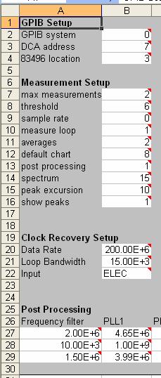
9 1 GPIB setup: Three entries define the addressing for how the computer communicates to the 86100C mainframe and 83496B clock recovery module: (a) GPIB system =: enter the address of the GPIB card that is connected to the 86100C mainframe in this location (b) DCA address =: enter the 86100C DCA-J GPIB address in this location (c) location =: enter the slot where the 83496B is installed (i) 1 for the left slot (ii) 3 for the right slot. 2 Measurement Setup (a) Max measurements: Sets the maximum number of phase noise measurements the system will make before processing and displaying the results. This effectively sets the number of acquisitions that will be obtained before the system process the data and displays the averaged result for all acquisitions. It is similar to setting the averaging factor for general oscilloscope waveform acquisition. Note that if the threshold value is exceeded (described below), the instrument will present the results before the prescribed number of waveforms have been obtained. (b) Threshold: This allows control of when data is saved and displayed. This parameter is based on the magnitude of the phase error at the output of the 83496B phase detector. When the magnitude of the error signal exceeds threshold value multiplied by the standard deviation of the error signal, the system will stop acquiring data and display the results. Thus the threshold value can stop acquisition prior to when the max measurement setting has been achieved. If the threshold value is never observed, the measurement will stop when the max measurement value has been met. When set to 0, each phase measurement will be recorded. For information on using this feature to capture a phase transient or glitch, see Appendix A below. (c) Sample rate: This selects the sample rate of the internal acquisition system. (i) 0= 40Ms/S. This setting enables measurement of the highest frequency jitter spectrum and phase noise possible ( 3 khz to 20 MHz offset) (ii) 64 = 4 Ms/S. This setting enables measuring as close to the carrier as possible (300 Hz to 2 MHz offset). (d) Measure Loop: This controls whether or not the loop response of the 83496B clock recovery module, having been locked to the signal being evaluated, will be measured. In most applications this should be set to 1 so the loop response will be measured. This then allows the system to compensate for the loop response and provide accurate results. If multiple measurements are to be made with a specific signal such that the 83496B
10 is not required to relock, earlier loop measurements are valid and the loop need not be re-measured. The setting can be 0. Note that if the data rate changes, or the pattern of a data signal changes, the loop should be measured to account for these changes. (e) Averages: This sets the number of measurements that are taken in the characterization of the loop bandwidth of the 83496B system and is generally not altered by the user. Note that this does not control how many measurements are acquired on the test signal (achieved with the max measurement parameter) and is only used as part of the test system characterization (f) Default Chart: This sets the priority for the charts that will be displayed. 5 is for the time display, 6 for the histogram display, and 8 for the jitter spectrum display. Regardless of the priority setting, all test results will be available by selecting the appropriate spreadsheet page. This control simply dictates which page will be displayed first. (g) Post processing: The measurement results can be further analyzed by processing them through a virtual network composed of two PLL s and a transport delay. The network is user definable. 1 enables post processing, 0 disables post processing. See Post Processing below (h) Spectrum: The system has the ability to display results from different points of view including the signal at the input to the 83496B (setting 15), the signal observed after passing through the dual-pll post processing function (setting 12, See Post Processing below), or the phase error observed at the output of the phase detector (setting 3) (i) Peak Excursion, Show Peaks: The jitter spectrum and phase noise displays may contain spectral lines when periodic jitter is present. It can be useful to determine the actual energy for these periodic tones. In the jitter spectrum plot, spectral tones are displayed in seconds versus frequency. Markers can be placed on these tones and when the computer cursor is placed on one of these markers, the signal level can be displayed. The marker will read out the jitter magnitude in seconds rms. The marker function will display the center of mass of the signal, which may be composed of multiple trace points. In the phase noise display, energy is displayed as the signal power normalized to a 1 Hz bandwidth relative to the carrier power. While this is useful for a noise spectrum, it can be problematic for spectral tones. Trace markers are designed to show the total signal power of the tone relative to the carrier, without being normalized to a 1 Hz bandwidth. This is similar to how periodic modulation is displayed on a spectrum analyzer. Thus the peak markers will be located at the x-axis position of the tone, but will be placed several db higher than the trace peak position. The marker readout is thus a dbc value rather than a dbc/hz value. When there are many discrete jitter tones, the ability to control when markers are placed and when they are not can prevent a cluttered display. This is achieved with the peak excursion and the show peaks parameters. The show peaks enables (1) or disables (0) the placement of markers. The peak excursion value
 Settings See Appendix A B.")
11 sets the minimum ratio of the signal to noise floor to receive a marker. When the value is large, only very prominent spectral lines will be marked. 3 To setup averaging in the frequency domain See Appendix B 4 Glitch Capture Mode (Advanced) Settings See Appendix A B. Clock Recovery Setup Note that several parameters for the 83496B clock recovery module can be controlled through the JSPN application or through the 86100CC mainframe user interface to the 83496B. The values entered into the JSPN application will override the manual settings made through the mainframe. To control the through the application, there are three entries available on the main setup page: Data rate, loop bandwidth, and input port. On the main setup page there is a section for clock recovery setup: 1 Set Data Rate (a) Click the Data Rate entry cell (b) Enter the data rate (as determined in section VI above) in the data rate block and press Enter on the PC keyboard 2 Set Loop Clock recovery Loop Bandwidth (a) Click the Loop Bandwidth entry cell (b) Enter the loop bandwidth (as determined in section VI above) in the loop bandwidth block and press enter on the PC keyboard. 3 Configure the input port: (a) Click the Input entry cell (b) Enter the Input port on the 83496B that is receiving the test signal: ELEC for the positive data port, EINV for the inverted data port, DIFF when using both electrical ports, and OPT for the optical port (83496B option 101) Once the clock recovery has been setup, the clock recovery hardware needs to be synchronized to the incoming signal. Press the Setup Clock Recovery key on the main setup page:

12 The JSPN application will perform a lock sequence on the test signal on the 83496B. (If the signal does not lock, verify that the settings match the test signal. You can also verify manually that the 83496B is capable of locking to the signal by operating the system from the 86100C mainframe front panel. Verify that the mainframe is in LOCAL mode by pressing the mainframe LOCAL key. The oscilloscope can also be used to verify the quality of the signal. If a reasonable waveform cannot be displayed, it may not be possible to perform a jitter spectrum/phase noise test). Post Processing The JSPN measurement results can be manipulated with a user defined network composed of two third-order PLLs, a transport delay, and a high-pass filter as shown below: The main reason for this feature is to implement the PCI-Express difference function, which is designed to assess the impact of the jitter of a signal as it would be seen by a receiver. Since the PCI-Express system uses a distributed clock, there will be a delay term altering the phase of the receiver clock relative to the phase of the clock used at the transmitter. Also, the PPL bandwidths of the transmitter and the receiver will not be identical. Thus when the reference clock jitter is measured, rather than determine its absolute performance, the signal is processed through a virtual network representing the PCI-Express system. The virtual network is defined in the post processing section of the Setup page. There are 8 parameters that can be defined:

13 For PLL1 there is a gain term (the frequency at which the PLL has unity gain), a pole frequency, and a zero frequency for a third order PLL model. For PLL2, similar gain frequency, pole frequency, and gain frequency parameters are entered. All values should be entered in Hertz. The difference function is defined by a high-pass filter frequency (in units of Hertz and a time difference accounting for the transport delay between the two PLLs is entered (in seconds). (Note that each cell has notation which is made visible by placing the cursor over the cell, indicating what parameter it accepts). The PCI-Express equations can be defined in terms of natural frequency and damping factor. Also, the PLL s can be second order rather than third order. To create a second order PLL, the pole frequency (second entry for each PLL) can be set to a large value, such as 1 GHz). To determine the gain and zero frequency entries from natural frequency and damping factor, the following equations are used: Gain frequency = natural frequency*damping factor*2 Zero frequency = Natural frequency/(2*damping factor) Post processing using the virtual network is enabled by setting the post processing cell in the measurement setup to 1. A 0 value disables the post processing. When enabled, the following measurements are made with the virtual network in place: Jitter spectrum Phase Noise spectrum Jitter versus time Frequency versus time Jitter histogram (note that the jitter histogram is only available when post processing is enabled) The following two measurements of a 2.5 GHz clock are made without and then with the virtual PLL system:
14 Jitter Spectrum Input Signal 1E-6 100E-9 10E-9 1E-9 Seconds (rms) 100E-12 10E-12 1E E-15 10E-15 1E E-18 10E-18 1E+3 10E+3 100E+3 1E+6 10E+6 100E+6 Jitter Spectrum / Phase Noise Application Beta 0.57 Delta Frequency (Hz) Clock jitter spectrum with no post-processing 1E-6 100E-9 10E-9 1E-9 100E-12 Jitter Spectrum Processed Signal Seconds (rms) 10E-12 1E E-15 10E-15 1E E-18 10E-18 1E E-21 1E+3 10E+3 100E+3 1E+6 10E+6 100E+6 Jitter Spectrum / Phase Noise Application Beta 0.57 Delta Frequency (Hz) Clock jitter spectrum with post-processing through the virtual PLL network Note that in the second jitter spectrum plot that the low frequency jitter is significantly reduced through the high-pass effect of the virtual PLL s.

15 The frequency versus time display is generated by differentiating the measured phase. Since frequency is the derivative of phase, and differentiation can sometimes generate artificial noise, a low-pass filter is available to smooth out this effect. The jitter spectrum can be processed to determine random, deterministic, and total jitter. The range of the spectrum to be processed is defined by the user through two filter settings. These filter settings for the spectral integration are also user-definable in the setup page under the post processing section. There are three frequency filter parameters that can be entered. The first is the low pass cutoff frequency used in the jitter versus time display. The second and third settings are for two filters that define the bandwidth for the jitter integrations. The allowable range of the frequency values is from 300 Hz to 2 MHz (when the sample rate is 40 MS/s) or 3 khz to 20 MHz (when the sample rate is set to 40 MS/s. Random jitter is determined through integration of the jitter spectrum, with the spectral tones removed, over three different bandwidths. The first is from the first filter frequency to the maximum frequency of the measurement (either 2 or 20 MHz, depending on the sample rate setting). The second bandwidth is from second filter frequency to the maximum frequency. The third bandwidth is the frequency range between the two filter settings. Deterministic jitter is determined over similar ranges. It is determined by taking the rms sum of all the spectral peaks of the jitter spectrum. Note that the user has control over the definition of what is determined to be a spectral peak, which can influence this result. Total jitter is determined by performing an RMS integration of the complete spectrum over the integration limits defined by the user. VIII Measuring jitter spectrum and phase noise A. Click the Measure Jitter button while on the main SETUP page.
16 B. Several things will now happen: 1 The application measures the loop response of the 83496B clock recovery circuit as it is locked to the signal being measured (if Measure Loop is set to 1). This data is recorded in the spreadsheet under tab databw E E+0 2.0E-6 4.0E-6 6.0E-6 8.0E E E E E-6 The above plot is essentially the response of the 83496B to an internally generated step (within the loop). This response is then used to back out the effects of the 83496B on the measured results. 2 The Phase Error (output of the phase detector in the clock recovery phase locked loop) will be recorded in the spreadsheet under tab DATA. The information provided here is useful only to the extent that it indicates that the loop response has been measured. There is no information relative to the signal being measured on this sheet. Each measurement is based on a 40 Ms/s or 4 Ms/s time record of points. Results are displayed as a function of time or transformed to be displayed in the (jitter) frequency domain. Because the loop response is known, it is possible to remove its response as well as view the signal from the perspective of the input to the 83496B or the output of the internal phase detector. 3 The most common view is the jitter spectrum (jitter in seconds versus jitter frequency) and phase noise (jitter power relative to the total signal power, normalized to a 1 Hz bandwidth, again versus jitter frequency. This is viewed
17 by selecting the Jitter Spectrum tab. The displayed result allows either the jitter spectrum or phase noise to be displayed. Jitter Spectrum 1E-6 100E-9 10E-9 1E-9 Seconds (rms) 100E-12 10E-12 1E E-15 10E-15 1E E-18 1E+3 10E+3 100E+3 1E+6 10E+6 100E+6 Delta Frequency (Hz) Jitter Spectrum / Phase Noise Application Beta 0.56 Phase Noise at 0.2GHz 000E+0-20E+0-40E+0-60E+0 dbc/hz -80E+0-100E+0-120E+0-140E+0-160E+0-180E+0 1E+3 10E+3 100E+3 1E+6 10E+6 100E+6 Delta Frequency (Hz) Jitter Spectrum / Phase Noise Application Beta 0.56
18 A toggle button (not shown here) allows switching between the jitter spectrum and phase noise displays. If the toggle button is not displayed on the graph, clicking on any of the spreadsheet cells should allow the button to be displayed. 4 The results can also be observed in the time domain. When the TIME tab is selected, two measurements are presented. Jitter versus time is a dual display. The pink trace is the phase modulation seen at the input of the 83496B phase detector. This plot helps indicate how the 83496B can track jitter and remove it from a general waveform analysis using the 86100C. Thus the pink input phase error is a measure of the total jitter observed by the 83496B. Note that since phase is the integral of frequency, if triangle shaped SSC frequency modulation were present, this display would be a parabolic shaped phase deviation. Viewing the input phase in the jitter domain provides an important troubleshooting capability. If there are ever phase transients, for example when a PLL loses synchronization or exceeds its allowable phase range, the phase glitch can be observed directly in the pink input phase trace. The blue phase error trace is an indication of the actual signal that the 86100C/83496B measurement system is observing. Below is the jitter vs time plot for a signal with SSC: Jitter vs. Time Phase Error (seconds) 200E E E-12 50E E+0-50E E E E E+0 50E-6 100E-6 150E-6 200E-6 250E-6 300E-6 350E-6 Time (seconds) 15E-9 10E-9 5E-9 000E+0-5E-9-10E-9-15E-9 Input Phase (seconds). 5 The blue trace on this graph helps indicate how the 83496B can track jitter and remove it from a general waveform analysis using the 86100C. Thus the pink input phase error is a measure of the total jitter observed by the 83496B. The blue phase error indicates the residual jitter not tracked by the 83496B. It is simply an indicator of how hard the 83496B phase lock loop is working to track the incoming signal. If the input phase and the phase error were similar, it would indicate that the 83496B PLL is not tracking the input signal. Note that the axes for the input phase error are orders of magnitude larger than the vertical axis for the phase error. 6 The second plot for the TIME tab is delta frequency versus time. This simply displays the difference in frequency, compared to the ideal (jitter free)
19 frequency, of the input signal as a function of time. The example below is for the signal with SSC present. Frequency vs Time 15E+6 Delta Frequency (Hz) 10E+6 5E+6 000E+0-5E+6-10E+6-15E+6 000E+0 50E-6 100E-6 150E-6 200E-6 250E-6 300E-6 350E-6 Time (seconds) 7 The HISTOGRAM tab displays the test signal as it would be observed having gone through the post-processing function configured in the setup page. The post processing allows the measured signal to be passed through two virtual PLLs with a fixed transport delay between them. The loop bandwidths of the virtual PLL s can clean up the jitter, but the clean up is affected by any time delay the signal experiences traveling from one PLL to the other. There are two displays in this tab. The observed jitter, measured in seconds, can be displayed as a function of time. This is the upper plot. The probability density (how often the signal reaches a given jitter magnitude) is displayed in the lower plot. Jitter (seconds) 2E-12 2E-12 1E E E+0-500E- 15-1E-12-2E-12-2E-12 Observed Jitter 000E+0 50E-6 100E-6 150E-6 200E-6 250E-6 300E-6 350E-6 Time (seconds)
20 Observed Jitter Histogram E E-3 PDF (hits) E-3 1.0E-3 CDF+/ E E-6-6E-12-4E-12-2E E+0 2E-12 4E-12 6E-12 Jitter (seconds) The pink traces of the histograms represent the cumulative distribution functions for each half of the histogram. Note that the histogram result is only available when post processing is enabled. IX Interpreting the results There is a wealth of information available from the jitter spectrum and phase noise measurement results but what is of interest to the user depends on the particular signal being measured and issues being investigated. Some of the common insights are listed here: - Phase Noise and Jitter Spectrum Charts These charts have the same x-axis and plot shape but have differing vertical axes. The vertical axis for the Phase Noise plot is in dbc/hz and that chart looks like the typical phase noise plot. The vertical axis for the Jitter Spectrum chart is jitter in Seconds RMS. As already noted, periodic jitter is displayed as discrete spectral lines. However, there can be spurious spectral lines that are artifacts of the measurement process. At this point in time the jitter spectrum and phase noise measurement is not synchronized with the data pattern so it is possible some pattern effects can be seen in the measurement results. When evaluating a data signal composed of an even length repeating pattern it is possible for a small spike to be present if the difference between the pattern repetition rate (data rate/ pattern length) and a harmonic of the sample rate (4 Mb/s or 40 Mb/s) falls within the frequency measurement window. For odd length repeating patterns two small spikes can occur, one where the difference between the pattern repetition rate and a harmonic of the sample rate falls within the frequency measurement window and another at half that frequency. For example: Data Rate = Gb/s Sample Rate = 40 MHz
21 Frequency Measurement Window = 3kHz to 20 MHz Pattern Length = 127 Bits (odd) Pattern Repetition Rate = (9.953Gb/s)/127 bits = approx 78.4 Mhz Pattern Repetition/2 = 39.2 MHz Measurement spur possible at 80 MHz-78.4 MHz = 1.6 MHz Measurement spur possible at 40 MHz 39.2 MHz 800 khz The Results Page Most of the results produced by the JSPN application are graphical. However, some results are numerical. Specifically, the spectrum can be analyzed to determine its contribution to the overall random, deterministic, and total jitter of a signal. This is achieved by integrating the jitter spectrum over user defined bandwidths (defined above in Post Processing). The results page provides a summary of the numerical measurements that JSPN can make. Saving results
22 Since the JSPN application is based on a spreadsheet, saving the spreadsheet file will also save the current measurement results. However, the spreadsheet application is a very large file. Also, as the majority of the measurement information is graphical in nature, it can be complicated to transport spreadsheet based graphics to other applications. The memory and complexity problems of measurement result storage are solved through the Save Results function found on the Setup page. When this is executed, the graphic displays from the Jitter Spectrum, Time, and Histogram pages are saved as a file including the graphic images and does not include the supporting spreadsheet information, significantly reducing the file size. In addition to the graphics, the information from the Results page is also recorded. (Note that marker functions used on graphics on spreadsheet pages are not functional on the saved results images). Verifying system operation As long as the 83496B is capable of locking onto the signal being tested, the JSPN application should provide good measurement results. The JSPN application performs best with narrow loop bandwidth settings for the 83496B. However, complicated signals may require the to have a wider loop bandwidth to achieve lock. Use the lowest loop bandwidth for which a lock condition can be achieved. Verification of operation can be achieved by measuring a high quality signal generator producing a simple clock or sinusoid. Use of a high quality generator should yield a signal with low jitter spectrum noise (and low phase noise) providing an indication of the JSPN system ability to observe low jitter signals. Some examples of signal generators that might be used include the Agilent 8257D or 8267D. Any generator capable of producing a clock like signal at GHz frequencies will work, but signals with reduced spectral purity will result in higher jitter noise results. Basic system operation can still be confirmed. The ability to also produce a specific level of periodic jitter at a specific frequency will also help verify system operation. In the following example, a 2.5 GHz clock signal from an Agilent 8267D is measured. The Signal Studio software application is used to generate 0.1 UI of periodic jitter at 1.2 MHz. The following is the JSPN configuration: Data rate: 5E+09 (double the frequency when measuring a clock) Loop BW: Input: ELEC (single ended input to the 83496) When the application is run, including setting up the clock recovery and measuring the jitter, the following jitter spectrum is observed:
23 Jitter Spectrum Input Phase 1E-6 100E-9 10E-9 Seconds (rms) 1E-9 100E-12 10E-12 1E E-15 10E-15 1E E-18 10E-18 1E+3 10E+3 100E+3 1E+6 10E+6 100E+6 Delta Frequency (Hz) Jitter Spectrum / Phase Noise Application Beta 0.57 The 8267D has extremely low phase noise, thus the jitter spectrum is quite low, under 1 fs above 300 khz. The periodic jitter is seen as several tones, with the dominant tone at 1.2 MHz. There are also tones at 2.4 MHz and 3.6 MHz. These represent harmonic distortion components of the desired 1.2 MHz periodic jitter. Two important points need to be made. Note that the harmonic distortion components are several orders of magnitude smaller than the main tone (the y axis is logarithmic). Also, the very low phase noise of the source allows the distortion tones to be observed. More common digital communications signals often have jitter noise that would completely obscure these tones. In addition to the 1.2 MHz series of tones, there are also tones at approximately 950, 1900, and 2850 khz. These are tones from the switching power supply in the 83496B. Again, the ultra low jitter of the 8267D source allows these spurious tones to be observed. The magnitude of the 1.2 MHz tone can be confirmed by going to the results page. Time of Measurement Beta Revision 0.57 Left Module 86106B Right Module 83496B Data Rate 5E+09 Loop Bandwidth Transition Density Input ELEC Post Processing
24 Frequency filter PLL1 PLL2 Difference E+09 1E E Integrated Jitter TJ DJ RJ Integral f1 to fmax 7.49E E E-14 Integral f2 to fmax 4.05E E E-14 Difference f1 to f2 7.49E E E-14 Highest Peak Frequency Jitter (rms) 7.49E-12 Jitter (p-p) 2.12E-11 The jitter frequency is measured at Hz vs. an expected value of Hz. The magnitude of the jitter is 7.49 ps rms and 21.2 ps peak-peak. The system was set to produce 0.1 UI pp of sinusoidal jitter. At 5 Gb/s, 1 UI is 200 ps. Thus the 21 ps value is within 5% of the expected 20 ps pp value. The best way to gauge the magnitude of the random jitter, represented by the noise floor of the jitter spectrum, is to integrate it over a specific bandwidth. The maximum frequency range of the application is 20 MHz. The integration limits are defined as part of the post processing system and shown as Filter 1 and Filter 2 in the results page (and are used to set the integration limits whether or not the signal is processed through the virtual PLL s). In this setup the F1 filter value is 10 khz, F2 is 1.5 MHz. The integrated jitter from 10 khz to 20 MHz is 50.8 fs, from 1.5 MHz to 20 MHz is 26 fs, and from 10 khz to 1.5 MHz is 43 fs. This is all noted in the results table above. When the system is verified with a signal other than the one described above, the results will obviously be different. Results will depend on the quality of the source and the precision to which periodic jitter can be produced. As noisier sources are used, the integrated jitter spectrum will be larger. However, the example given should provide some levels that can be expected for specific conditions as well as an indication of the lower regions of what can be observed.
25 Appendix A: Transient/Glitch Capture Mode (Advanced) There may be situations where the signal being tested is normally well behaved but occasionally has a fault creating a significant phase error component. An example where this may occur is when the phase detector in a clock multiplier circuit phase wraps (phase exceeds +/- p). In this case it is desirable to evaluate the signal over a long period of time and record the measurement only when the large phase error occurs. The JSPN Application can help to measure this phenomenon in the Glitch Capture Mode. To run in the Glitch Capture Mode follow the General Settings in section VII and then the instructions below: A. Threshold: This value, which is (peak phase error)/sigma, sets the threshold to trigger saving data and recording a jitter spectrum and phase noise measurement Thus a transient event will be captured if the phase error exceeds the standard deviation of the overall phase error by the threshold value. To operate in the Glitch Capture Mode some trial and error may be required to determine the ideal threshold value. Setting threshold too low may cause the instrument to trigger on events that are not significant. Setting the threshold too high may result in the phase transient never being captured. A typical starting point would be a threshold of 2, which would cause the system to trip when the phase error is double the overall standard deviation. If the system achieves the maximum measurement, the system will stop without having been triggered by a phase transient. The threshold should be decreased. If the system trips on signals other than the event that is being sought, the threshold value should be increased. B. Measure Loop: This defines if the loop response of the 83496B clock recovery module, as locked to the signal being evaluated, will be measured. If the 83496B clock recovery module is already locked to the signal being evaluated and a standard Jitter spectrum and phase noise measurement has already been run, the JSPN Application has evaluated and recorded the loop response and further measurements of the loop are not required. If that is the case, set this value to 0 so further loop measurements are not made, enabling the application to run faster. If the loop has not yet been evaluated or has been re-locked since the last time the loop was evaluated, set this value to 1 so the loop response can be measured. C. Max Measurements: Sets the maximum number of measurements the application will make as it looks for a phase error that meets the Threshold criteria. Setting this value to a large number will allow the application to make many measurements as it looks for a phase error that meets the Threshold you have set above. However, the application will not stop until it has either: 1 found a phase error that meets the Threshold set above, or 2 measured the signal the number of times set for Max Measurements Notes: A high Threshold setting combined with a large value for Max Measurements will result in a long test time. If the threshold is reached the Phase Error chart will show the result of only the last measurement (where the threshold was reached) and the Phase Noise and Jitter Spectrum charts will be averaged over all the measurements taken.
26 . Appendix B Averaging the Measurement in the Frequency Domain To minimize noise in the frequency response plots you can set up the measurement to average in the frequency domain (the phase error in the time domain will not be averaged). To average in the frequency domain follow the General Settings in section VII and then the instructions below: A. Threshold: This sets the phase error threshold to trigger the saving data process and records a jitter spectrum and/or phase noise measurement. Set to a large number such as 100, this state is likely never reached, allowing the desired number of averages to be completed before the data is recorded and processed. B. Measure Loop: This defines if the loop response of the 83496B clock recovery module, as locked to the signal being evaluated, will be measured. Set to 1 so the loop response will be measured. C. Max Measurements: Sets to the number of averages desired. Appendix C Measuring signals below 50 Mb/s Note that the minimum data rate supported by the 83496B clock recovery module is 50 Mb/s, indicating the minimum data rate supported by the JSPN Application is 50 Mb/s or a 25 MHz clock. However, depending on your data pattern, you may be able to lock the clock recovery module to a slower data rate or slower clock. A. A pattern at 25 Mb/s looks just like a pattern at 50 Mb/s. A clock signal is just a special case where the pattern is a repeating If you have a signal you need to evaluate that is below the minimum rate (50 Mb/s) supported by the 83496B you can try to lock the clock recovery module to that signal by telling the clock recovery module the signal is 2, 3 or 4 times faster than the actual data rate. B. The clock recovery circuit then just considers each bit in the pattern to be 2, 3 or 4 consecutive identical bits. Provided the clock recovery module can lock to the signal, the jitter spectrum and phase noise measurement results will not be affected by this approach.
Real Time Jitter Analysis
 Real Time Jitter Analysis Agenda ı Background on jitter measurements Definition Measurement types: parametric, graphical ı Jitter noise floor ı Statistical analysis of jitter Jitter structure Jitter PDF
Agilent Technologies PSA Series Spectrum Analyzers Test and Adjustment Software
 Test System Overview Agilent Technologies PSA Series Spectrum Analyzers Test and Adjustment Software Test System Overview The Agilent Technologies test system is designed to verify the performance of the
Noise Measurements Using a Teledyne LeCroy Oscilloscope
 Noise Measurements Using a Teledyne LeCroy Oscilloscope TECHNICAL BRIEF January 9, 2013 Summary Random noise arises from every electronic component comprising your circuits. The analysis of random electrical
Picking the Optimal Oscilloscope for Serial Data Signal Integrity Validation and Debug
 Picking the Optimal Oscilloscope for Serial Data Signal Integrity Validation and Debug Application Note 1556 Introduction In the past, it was easy to decide whether to use a real-time oscilloscope or an
Models 296 and 295 combine sophisticated
 Established 1981 Advanced Test Equipment Rentals www.atecorp.com 800-404-ATEC (2832) Models 296 and 295 50 MS/s Synthesized Multichannel Arbitrary Waveform Generators Up to 4 Independent Channels 10 Standard
SHF Communication Technologies AG. Wilhelm-von-Siemens-Str. 23D Berlin Germany. Phone Fax
 SHF Communication Technologies AG Wilhelm-von-Siemens-Str. 23D 12277 Berlin Germany Phone +49 30 772051-0 Fax ++49 30 7531078 E-Mail: sales@shf.de Web: http://www.shf.de Application Note Jitter Injection
Advanced Lab LAB 6: Signal Acquisition & Spectrum Analysis Using VirtualBench DSA Equipment: Objectives:
 Advanced Lab LAB 6: Signal Acquisition & Spectrum Analysis Using VirtualBench DSA Equipment: Pentium PC with National Instruments PCI-MIO-16E-4 data-acquisition board (12-bit resolution; software-controlled
Jitter Measurements using Phase Noise Techniques
 Jitter Measurements using Phase Noise Techniques Agenda Jitter Review Time-Domain and Frequency-Domain Jitter Measurements Phase Noise Concept and Measurement Techniques Deriving Random and Deterministic
Computing TIE Crest Factors for Telecom Applications
 TECHNICAL NOTE Computing TIE Crest Factors for Telecom Applications A discussion on computing crest factors to estimate the contribution of random jitter to total jitter in a specified time interval. by
Gentec-EO USA. T-RAD-USB Users Manual. T-Rad-USB Operating Instructions /15/2010 Page 1 of 24
 Gentec-EO USA T-RAD-USB Users Manual Gentec-EO USA 5825 Jean Road Center Lake Oswego, Oregon, 97035 503-697-1870 voice 503-697-0633 fax 121-201795 11/15/2010 Page 1 of 24 System Overview Welcome to the
P a g e 1 ST985. TDR Cable Analyzer Instruction Manual. Analog Arts Inc.
 P a g e 1 ST985 TDR Cable Analyzer Instruction Manual Analog Arts Inc. www.analogarts.com P a g e 2 Contents Software Installation... 4 Specifications... 4 Handling Precautions... 4 Operation Instruction...
Jitter Analysis Techniques Using an Agilent Infiniium Oscilloscope
 Jitter Analysis Techniques Using an Agilent Infiniium Oscilloscope Product Note Table of Contents Introduction........................ 1 Jitter Fundamentals................. 1 Jitter Measurement Techniques......
SV2C 28 Gbps, 8 Lane SerDes Tester
 SV2C 28 Gbps, 8 Lane SerDes Tester Data Sheet SV2C Personalized SerDes Tester Data Sheet Revision: 1.0 2015-03-19 Revision Revision History Date 1.0 Document release. March 19, 2015 The information in
ArbStudio Arbitrary Waveform Generators
 ArbStudio Arbitrary Waveform Generators Key Features Outstanding performance with 16-bit, 1 GS/s sample rate and 2 Mpts/Ch 2 and 4 channel models Digital pattern generator PWM mode Sweep and burst modes
PXIe Contents CALIBRATION PROCEDURE. Reconfigurable 6 GHz RF Vector Signal Transceiver with 200 MHz Bandwidth
 IBRATION PROCEDURE PXIe-5646 Reconfigurable 6 GHz Vector Signal Transceiver with 200 MHz Bandwidth This document contains the verification and adjustment procedures for the PXIe-5646 vector signal transceiver.
Keysight Technologies PNA-X Series Microwave Network Analyzers
 Keysight Technologies PNA-X Series Microwave Network Analyzers Active-Device Characterization in Pulsed Operation Using the PNA-X Application Note Introduction Vector network analyzers (VNA) are the common
Laboratory Experiment #1 Introduction to Spectral Analysis
 J.B.Francis College of Engineering Mechanical Engineering Department 22-403 Laboratory Experiment #1 Introduction to Spectral Analysis Introduction The quantification of electrical energy can be accomplished
RF Signal Generators. SG380 Series DC to 2 GHz, 4 GHz and 6 GHz analog signal generators. SG380 Series RF Signal Generators
 RF Signal Generators SG380 Series DC to 2 GHz, 4 GHz and 6 GHz analog signal generators SG380 Series RF Signal Generators DC to 2 GHz, 4 GHz or 6 GHz 1 µhz resolution AM, FM, ΦM, PM and sweeps OCXO timebase
High Speed Digital Design & Verification Seminar. Measurement fundamentals
 High Speed Digital Design & Verification Seminar Measurement fundamentals Agenda Sources of Jitter, how to measure and why Importance of Noise Select the right probes! Capture the eye diagram Why measure
Model 7000 Series Phase Noise Test System
 Established 1981 Advanced Test Equipment Rentals www.atecorp.com 800-404-ATEC (2832) Model 7000 Series Phase Noise Test System Fully Integrated System Cross-Correlation Signal Analysis to 26.5 GHz Additive
APPH6040B / APPH20G-B Specification V2.0
 APPH6040B / APPH20G-B Specification V2.0 (July 2014, Serial XXX-XX33XXXXX-XXXX or higher) A fully integrated high-performance cross-correlation signal source analyzer for to 7 or 26 GHz 1 Introduction
Agilent E5505A Phase Noise Measurement System
 Agilent E5505A Phase Noise Measurement System Notice: This document contains references to Agilent. Please note that Agilent s Test and Measurement business has become Keysight Technologies. For more information,
1 Introduction: frequency stability and accuracy
 Content 1 Introduction: frequency stability and accuracy... Measurement methods... 4 Beat Frequency method... 4 Advantages... 4 Restrictions... 4 Spectrum analyzer method... 5 Advantages... 5 Restrictions...
Keysight Technologies Precision Jitter Analysis Using the Keysight 86100C DCA-J. Application Note
 Keysight Technologies Precision Jitter Analysis Using the Keysight 86100C DCA-J Application Note Introduction The extremely wide bandwidth of equivalent-time sampling oscilloscopes makes them the tool
Testing with Femtosecond Pulses
 Testing with Femtosecond Pulses White Paper PN 200-0200-00 Revision 1.3 January 2009 Calmar Laser, Inc www.calmarlaser.com Overview Calmar s femtosecond laser sources are passively mode-locked fiber lasers.
DCNTS Phase Noise Analyzer 2 MHz to 1.8 / 26 / 50 / 140 GHz
 DCNTS Phase Noise Analyzer 2 MHz to 1.8 / 26 / 50 / 140 GHz Datasheet The DCNTS is the highest performance Phase Noise Analyzer with unique flexible capabilities as summarized below: Phase Noise Amplitude
PGT313 Digital Communication Technology. Lab 3. Quadrature Phase Shift Keying (QPSK) and 8-Phase Shift Keying (8-PSK)
 and 8-Phase Shift Keying (8-PSK)") PGT313 Digital Communication Technology Lab 3 Quadrature Phase Shift Keying (QPSK) and 8-Phase Shift Keying (8-PSK) Objectives i) To study the digitally modulated quadrature phase shift keying (QPSK) and
PGT313 Digital Communication Technology Lab 3 Quadrature Phase Shift Keying (QPSK) and 8-Phase Shift Keying (8-PSK) Objectives i) To study the digitally modulated quadrature phase shift keying (QPSK) and
Advanced Test Equipment Rentals ATEC (2832)
") Established 1981 Advanced Test Equipment Rentals www.atecorp.com 800-404-ATEC (2832) Electric and Magnetic Field Measurement For Isotropic Measurement of Magnetic and Electric Fields Evaluation of Field
Established 1981 Advanced Test Equipment Rentals www.atecorp.com 800-404-ATEC (2832) Electric and Magnetic Field Measurement For Isotropic Measurement of Magnetic and Electric Fields Evaluation of Field
Quick Start Guide for the PULSE PROFILING APPLICATION
 Quick Start Guide for the PULSE PROFILING APPLICATION MODEL LB480A Revision: Preliminary 02/05/09 1 1. Introduction This document provides information to install and quickly start using your PowerSensor+.
PXIe Contents SPECIFICATIONS. 14 GHz and 26.5 GHz Vector Signal Analyzer
 SPECIFICATIONS PXIe-5668 14 GHz and 26.5 GHz Vector Signal Analyzer These specifications apply to the PXIe-5668 (14 GHz) Vector Signal Analyzer and the PXIe-5668 (26.5 GHz) Vector Signal Analyzer with
Using Frequency Diversity to Improve Measurement Speed Roger Dygert MI Technologies, 1125 Satellite Blvd., Suite 100 Suwanee, GA 30024
 Using Frequency Diversity to Improve Measurement Speed Roger Dygert MI Technologies, 1125 Satellite Blvd., Suite 1 Suwanee, GA 324 ABSTRACT Conventional antenna measurement systems use a multiplexer or
Keysight Technologies Making Accurate Intermodulation Distortion Measurements with the PNA-X Network Analyzer, 10 MHz to 26.5 GHz
 Keysight Technologies Making Accurate Intermodulation Distortion Measurements with the PNA-X Network Analyzer, 10 MHz to 26.5 GHz Application Note Overview This application note describes accuracy considerations
Troubleshooting Common EMI Problems
 By William D. Kimmel, PE Kimmel Gerke Associates, Ltd. Learn best practices for troubleshooting common EMI problems in today's digital designs. Industry expert William Kimmel of Kimmel Gerke Associates
SpinCore RadioProcessor LabVIEW Extensions
 NMR Interface User's Manual SpinCore Technologies, Inc. http:// Congratulations and thank you for choosing a design from SpinCore Technologies, Inc. We appreciate your business! At SpinCore we try to fully
Digital Waveform with Jittered Edges. Reference edge. Figure 1. The purpose of this discussion is fourfold.
 Joe Adler, Vectron International Continuous advances in high-speed communication and measurement systems require higher levels of performance from system clocks and references. Performance acceptable in
University of New Hampshire InterOperability Laboratory Gigabit Ethernet Consortium
 University of New Hampshire InterOperability Laboratory Gigabit Ethernet Consortium As of June 18 th, 2003 the Gigabit Ethernet Consortium Clause 40 Physical Medium Attachment Conformance Test Suite Version
Generating Jitter for Fibre Channel Compliance Testing
 Application Note: HFAN-4.5.2 Rev 0; 12/00 Generating Jitter for Fibre Channel Compliance Testing MAXIM High-Frequency/Fiber Communications Group 4hfan452.doc 01/02/01 Generating Jitter for Fibre Channel
How to Setup a Real-time Oscilloscope to Measure Jitter
 TECHNICAL NOTE How to Setup a Real-time Oscilloscope to Measure Jitter by Gary Giust, PhD NOTE-3, Version 1 (February 16, 2016) Table of Contents Table of Contents... 1 Introduction... 2 Step 1 - Initialize
Keysight Technologies Phase Noise X-Series Measurement Application
 Keysight Technologies Phase Noise X-Series Measurement Application N9068C Technical Overview Phase noise measurements with log plot and spot frequency views Spectrum and IQ waveform monitoring for quick
FlexDDS-NG DUAL. Dual-Channel 400 MHz Agile Waveform Generator
 FlexDDS-NG DUAL Dual-Channel 400 MHz Agile Waveform Generator Excellent signal quality Rapid parameter changes Phase-continuous sweeps High speed analog modulation Wieserlabs UG www.wieserlabs.com FlexDDS-NG
Phase Noise Measurement Personality for the Agilent ESA-E Series Spectrum Analyzers
 Phase Noise Measurement Personality for the Agilent ESA-E Series Spectrum Analyzers Product Overview Now the ESA-E series spectrum analyzers have one-button phase noise measurements, including log plot,
ArbStudio Arbitrary Waveform Generators. Powerful, Versatile Waveform Creation
 ArbStudio Arbitrary Waveform Generators Powerful, Versatile Waveform Creation UNMATCHED WAVEFORM UNMATCHED WAVEFORM GENERATION GENERATION Key Features 125 MHz bandwidth 1 GS/s maximum sample rate Long
Fourier Theory & Practice, Part II: Practice Operating the Agilent Series Scope with Measurement/Storage Module
 Fourier Theory & Practice, Part II: Practice Operating the Agilent 54600 Series Scope with Measurement/Storage Module By: Robert Witte Agilent Technologies Introduction: This product note provides a brief
N9051A Pulse Measurement Software
 N9051A Pulse Measurement Software X-Series Signal Analyzers and PSA Series Spectrum Analyzers Technical Overview Characterize pulse performance using a wide range of parameters including pulse width, rise/fall
RF Signal Generators. SG380 Series DC to 2 GHz, 4 GHz and 6 GHz analog signal generators. SG380 Series RF Signal Generators
 RF Signal Generators SG380 Series DC to 2 GHz, 4 GHz and 6 GHz analog signal generators SG380 Series RF Signal Generators DC to 2 GHz, 4 GHz or 6 GHz 1 μhz resolution AM, FM, ΦM, PM and sweeps OCXO timebase
Keysight Technologies 8 Hints for Making Better Measurements Using RF Signal Generators. Application Note
 Keysight Technologies 8 Hints for Making Better Measurements Using RF Signal Generators Application Note 02 Keysight 8 Hints for Making Better Measurements Using RF Signal Generators - Application Note
Keysight X-Series Signal Analyzers
 Keysight X-Series Signal Analyzers This manual provides documentation for the following models: N9040B UXA N9030B PXA N9020B MXA N9010B EXA N9000B CXA N9068C Phase Noise Measurement Application Measurement
WaveStation Function/Arbitrary Waveform Generators
 WaveStation Function/Arbitrary Waveform Generators Key Features High performance with 14-bit, 125 MS/s and 16 kpts 2 channels on all models Large 3.5 color display for easy waveform preview Over 40 built-in
Advanced Signal Integrity Measurements of High- Speed Differential Channels
 Advanced Signal Integrity Measurements of High- Speed Differential Channels September 2004 presented by: Mike Resso Greg LeCheminant Copyright 2004 Agilent Technologies, Inc. What We Will Discuss Today
WaveStation Function/Arbitrary Waveform Generators
 WaveStation Function/Arbitrary Waveform Generators Key Features High performance with 14-bit, 125 MS/s and 16 kpts 2 channels on all models Large 3.5 color display for easy waveform preview Over 40 built-in
Your Network. Optimized.
 Over 20 years of research both at the National Institute of Standards and Technology (NIST) and in private industry have been dedicated to the research and development of Symmetricom s phase noise and
WaveStation Function/Arbitrary Waveform Generators
 Function/Arbitrary Waveform Generators Key Features High performance with 14-bit waveform generation, up to 500 MS/s sample rate and up to 512 kpts memory 2 channels on all models Large color display for
PXI UMTS Uplink Measurement Suite Data Sheet
 PXI UMTS Uplink Measurement Suite Data Sheet The most important thing we build is trust A production ready ATE solution for RF alignment and performance verification Tx Max Output Power Frequency Error
ECE 440L. Experiment 1: Signals and Noise (1 week)
") ECE 440L Experiment 1: Signals and Noise (1 week) I. OBJECTIVES Upon completion of this experiment, you should be able to: 1. Use the signal generators and filters in the lab to generate and filter noise
ECE 440L Experiment 1: Signals and Noise (1 week) I. OBJECTIVES Upon completion of this experiment, you should be able to: 1. Use the signal generators and filters in the lab to generate and filter noise
Glossary of VCO terms
 Glossary of VCO terms VOLTAGE CONTROLLED OSCILLATOR (VCO): This is an oscillator designed so the output frequency can be changed by applying a voltage to its control port or tuning port. FREQUENCY TUNING
3.2 Measuring Frequency Response Of Low-Pass Filter :
 2.5 Filter Band-Width : In ideal Band-Pass Filters, the band-width is the frequency range in Hz where the magnitude response is at is maximum (or the attenuation is at its minimum) and constant and equal
IEEE 802.3aq Task Force Dynamic Channel Model Ad Hoc Task 2 - Time variation & modal noise 10/13/2004 con-call
 IEEE 802.3aq Task Force Dynamic Channel Model Ad Hoc Task 2 - Time variation & modal noise 10/13/2004 con-call Time variance in MMF links Further test results Rob Coenen Overview Based on the formulation
UCE-DSO212 DIGITAL OSCILLOSCOPE USER MANUAL. UCORE ELECTRONICS
 UCE-DSO212 DIGITAL OSCILLOSCOPE USER MANUAL UCORE ELECTRONICS www.ucore-electronics.com 2017 Contents 1. Introduction... 2 2. Turn on or turn off... 3 3. Oscilloscope Mode... 4 3.1. Display Description...
2801 Multilock. Communications System Analyzer. Data Sheet. Boosting wireless efficiency
 Data Sheet 2801 Multilock Communications System Analyzer Boosting wireless efficiency A real multi-talented instrument the Willtek 2801 Multilock The Willtek 2801 Multilock is a test instrument for multiple
Basic Communication Laboratory Manual. Shimshon Levy&Harael Mualem
 Basic Communication Laboratory Manual Shimshon Levy&Harael Mualem September 2006 CONTENTS 1 The oscilloscope 2 1.1 Objectives... 2 1.2 Prelab... 2 1.3 Background Theory- Analog Oscilloscope...... 3 1.4
LNS ultra low phase noise Synthesizer 8 MHz to 18 GHz
 LNS ultra low phase noise Synthesizer 8 MHz to 18 GHz Datasheet The LNS is an easy to use 18 GHz synthesizer that exhibits outstanding phase noise and jitter performance in a 3U rack mountable chassis.
Impedance 50 (75 connectors via adapters)
") VECTOR NETWORK ANALYZER PLANAR 304/1 DATA SHEET Frequency range: 300 khz to 3.2 GHz Measured parameters: S11, S21, S12, S22 Dynamic range of transmission measurement magnitude: 135 db Measurement time
VECTOR NETWORK ANALYZER PLANAR 304/1 DATA SHEET Frequency range: 300 khz to 3.2 GHz Measured parameters: S11, S21, S12, S22 Dynamic range of transmission measurement magnitude: 135 db Measurement time
Reconfigurable 6 GHz Vector Signal Transceiver with I/Q Interface
 SPECIFICATIONS PXIe-5645 Reconfigurable 6 GHz Vector Signal Transceiver with I/Q Interface Contents Definitions...2 Conditions... 3 Frequency...4 Frequency Settling Time... 4 Internal Frequency Reference...
ETSI Standards and the Measurement of RF Conducted Output Power of Wi-Fi ac Signals
 ETSI Standards and the Measurement of RF Conducted Output Power of Wi-Fi 802.11ac Signals Introduction The European Telecommunications Standards Institute (ETSI) have recently introduced a revised set
SDI. Table of Contents
 NMSC-2 User Manual 2 Table of Contents Introduction........ 4 Hardware Installation.... 5 NMSC Power On.. 8 Overview... 9 FFT Measurement Screen.. 10 FFT Setup..... 11 FFT Detector..... 14 FFT Calibration.....
SYSTEM ONE * DSP SYSTEM ONE DUAL DOMAIN (preliminary)
") SYSTEM ONE * DSP SYSTEM ONE DUAL DOMAIN (preliminary) Audio Precision's new System One + DSP (Digital Signal Processor) and System One Deal Domain are revolutionary additions to the company's audio testing
SYSTEM ONE * DSP SYSTEM ONE DUAL DOMAIN (preliminary) Audio Precision's new System One + DSP (Digital Signal Processor) and System One Deal Domain are revolutionary additions to the company's audio testing
Analog Arts SF900 SF650 SF610 Product Specifications
 www.analogarts.com Analog Arts SF900 SF650 SF610 Product Specifications Analog Arts reserves the right to change, modify, add or delete portions of any one of its specifications at any time, without prior
Addressing the Challenges of Wideband Radar Signal Generation and Analysis. Marco Vivarelli Digital Sales Specialist
 Addressing the Challenges of Wideband Radar Signal Generation and Analysis Marco Vivarelli Digital Sales Specialist Agenda Challenges of Wideband Signal Generation Challenges of Wideband Signal Analysis
Keysight Technologies BER Measurement Using a Real-Time Oscilloscope Controlled From M8070A. Application Note
 Keysight Technologies BER Measurement Using a Real-Time Oscilloscope Controlled From M8070A Application Note 02 Keysight BER Measurement Using Real-Time Oscilloscope Controlled from M8070A - Application
The Fundamentals of Mixed Signal Testing
 The Fundamentals of Mixed Signal Testing Course Information The Fundamentals of Mixed Signal Testing course is designed to provide the foundation of knowledge that is required for testing modern mixed
Lab 4. Crystal Oscillator
 Lab 4. Crystal Oscillator Modeling the Piezo Electric Quartz Crystal Most oscillators employed for RF and microwave applications use a resonator to set the frequency of oscillation. It is desirable to
Switched Mode Power Supply Measurements
 Power Analysis 1 Switched Mode Power Supply Measurements AC Input Power measurements Safe operating area Harmonics and compliance Efficiency Switching Transistor Losses Measurement challenges Transformer
Limitations And Accuracies Of Time And Frequency Domain Analysis Of Physical Layer Devices
 Limitations And Accuracies Of Time And Frequency Domain Analysis Of Physical Layer Devices Outline Short Overview Fundamental Differences between TDR & Instruments Calibration & Normalization Measurement
Analog Arts SF990 SF880 SF830 Product Specifications
 1 www.analogarts.com Analog Arts SF990 SF880 SF830 Product Specifications Analog Arts reserves the right to change, modify, add or delete portions of any one of its specifications at any time, without
Analog Arts SL987 SL957 SL937 SL917 Product Specifications [1]
![Analog Arts SL987 SL957 SL937 SL917 Product Specifications [1]](/thumbs/95/126095980.jpg "Analog Arts SL987 SL957 SL937 SL917 Product Specifications [1]") www.analogarts.com Analog Arts SL987 SL957 SL937 SL917 Product Specifications [1] 1. These models include: an oscilloscope, a spectrum analyzer, a data recorder, a frequency & phase meter, an arbitrary
www.analogarts.com Analog Arts SL987 SL957 SL937 SL917 Product Specifications [1] 1. These models include: an oscilloscope, a spectrum analyzer, a data recorder, a frequency & phase meter, an arbitrary
LAB #7: Digital Signal Processing
 LAB #7: Digital Signal Processing Equipment: Pentium PC with NI PCI-MIO-16E-4 data-acquisition board NI BNC 2120 Accessory Box VirtualBench Instrument Library version 2.6 Function Generator (Tektronix
RLC Software User s Manual
 RLC Software User s Manual Venable Instruments 4201 S. Congress, Suite 201 Austin, TX 78745 512-837-2888 www.venable.biz Introduction The RLC software allows you to measure the frequency response of RLC
Agilent Correlation between TDR oscilloscope and VNA generated time domain waveform
 Agilent Correlation between TDR oscilloscope and VNA generated time domain waveform Application Note Introduction Time domain analysis (TDA) is a common method for evaluating transmission lines and has
Keysight Technologies N9051B Pulse Measurement Software X-Series Signal Analyzers. Technical Overview
 Keysight Technologies N9051B Pulse Measurement Software X-Series Signal Analyzers Technical Overview 02 Keysight N9051B Pulse Measurement Software X-Series Signal Analyzers - Technical Overview Features
Characterize Phase-Locked Loop Systems Using Real Time Oscilloscopes
 Characterize Phase-Locked Loop Systems Using Real Time Oscilloscopes Introduction Phase-locked loops (PLL) are frequently used in communication applications. For example, they recover the clock from digital
Analog Arts SG985 SG884 SG834 SG814 Product Specifications [1]
![Analog Arts SG985 SG884 SG834 SG814 Product Specifications [1]](/thumbs/94/122371203.jpg "Analog Arts SG985 SG884 SG834 SG814 Product Specifications [1]") www.analogarts.com Analog Arts SG985 SG884 SG834 SG814 Product Specifications [1] 1. These models include: an oscilloscope, a spectrum analyzer, a data recorder, a frequency & phase meter, and an arbitrary
www.analogarts.com Analog Arts SG985 SG884 SG834 SG814 Product Specifications [1] 1. These models include: an oscilloscope, a spectrum analyzer, a data recorder, a frequency & phase meter, and an arbitrary
771 Series LASER SPECTRUM ANALYZER. The Power of Precision in Spectral Analysis. It's Our Business to be Exact! bristol-inst.com
 771 Series LASER SPECTRUM ANALYZER The Power of Precision in Spectral Analysis It's Our Business to be Exact! bristol-inst.com The 771 Series Laser Spectrum Analyzer combines proven Michelson interferometer
Table 1: Cross Reference of Applicable Products
 Standard Product UT7R995/C RadClock Jitter Performance Application Note January 21, 2016 The most important thing we build is trust Table 1: Cross Reference of Applicable Products PRODUCT NAME RadClock
Gigabit Ethernet Consortium Clause 38 PMD Conformance Test Suite v.7 Report
 Gigabit Ethernet Consortium Clause 38 PMD Conformance Test Suite v.7 Report UNH-IOL 121 Technology Drive, Suite 2 Durham, NH 3824 +1-63-862-9 GE Consortium Manager: Gerard Nadeau grn@iol.unh.edu +1-63-862-166
What the LSA1000 Does and How
 2 About the LSA1000 What the LSA1000 Does and How The LSA1000 is an ideal instrument for capturing, digitizing and analyzing high-speed electronic signals. Moreover, it has been optimized for system-integration
8 Hints for Better Spectrum Analysis. Application Note
 8 Hints for Better Spectrum Analysis Application Note 1286-1 The Spectrum Analyzer The spectrum analyzer, like an oscilloscope, is a basic tool used for observing signals. Where the oscilloscope provides
Keysight Technologies E8257D PSG Microwave Analog Signal Generator. Data Sheet
 Keysight Technologies E8257D PSG Microwave Analog Signal Generator Data Sheet 02 Keysight E8257D Microwave Analog Signal Generator - Data Sheet Table of Contents Specifications... 4 Frequency... 4 Step
New Features of IEEE Std Digitizing Waveform Recorders
 New Features of IEEE Std 1057-2007 Digitizing Waveform Recorders William B. Boyer 1, Thomas E. Linnenbrink 2, Jerome Blair 3, 1 Chair, Subcommittee on Digital Waveform Recorders Sandia National Laboratories
Agilent N5411A Serial ATA Electrical Performance Validation and Compliance Software Release Notes
 Agilent N5411A Serial ATA Electrical Performance Validation and Compliance Software Release Notes Agilent N5411A Software Version 2.60 Released Date: 7 Nov 2008 Minimum Infiniium Oscilloscope Baseline
Contents. ZT530PCI & PXI Specifications. Arbitrary Waveform Generator. 16-bit, 400 MS/s, 2 Ch
 ZT530PCI & PXI Specifications Arbitrary Waveform Generator 16-bit, 400 MS/s, 2 Ch Contents Outputs... 2 Digital-to-Analog Converter (DAC)... 3 Internal DAC Clock... 3 Spectral Purity... 3 External DAC
SIGNAL RECOVERY. Model 7265 DSP Lock-in Amplifier
 Model 7265 DSP Lock-in Amplifier FEATURES 0.001 Hz to 250 khz operation Voltage and current mode inputs Direct digital demodulation without down-conversion 10 µs to 100 ks output time constants Quartz
R&S NRP-Zxx Power Sensors Specifications
 R&S NRP-Zxx Power Sensors Specifications year Data Sheet Version 11.00 CONTENTS Definitions... 3 Overview of the R&S NRP-Zxx power sensors... 4 Specifications in brief of the R&S NRP-Zxx power sensors...
PN9000 PULSED CARRIER MEASUREMENTS
 The specialist of Phase noise Measurements PN9000 PULSED CARRIER MEASUREMENTS Carrier frequency: 2.7 GHz - PRF: 5 khz Duty cycle: 1% Page 1 / 12 Introduction When measuring a pulse modulated signal the
DSA700 Series Spectrum Analyzer
 DSA700 Series Spectrum Analyzer Product Features: All-Digital IF Technology Frequency Range from 100 khz up to 1 GHz Min. -155 dbm Displayed Average Noise Level (Typ.) Min.
Accurate Phase Noise Measurements Made Cost Effective
 MTTS 2008 MicroApps Accurate Phase Noise Measurements Made Cost Effective author : Jason Breitbarth, PhD. Boulder, Colorado, USA Presentation Outline Phase Noise Intro Additive and Absolute Oscillator
UCE-DSO210 DIGITAL OSCILLOSCOPE USER MANUAL. FATIH GENÇ UCORE ELECTRONICS REV1
 UCE-DSO210 DIGITAL OSCILLOSCOPE USER MANUAL FATIH GENÇ UCORE ELECTRONICS www.ucore-electronics.com 2017 - REV1 Contents 1. Introduction... 2 2. Turn on or turn off... 3 3. Oscilloscope Mode... 3 3.1. Display
Enhancing Analog Signal Generation by Digital Channel Using Pulse-Width Modulation
 Enhancing Analog Signal Generation by Digital Channel Using Pulse-Width Modulation Angelo Zucchetti Advantest angelo.zucchetti@advantest.com Introduction Presented in this article is a technique for generating
IX Feb Operation Guide. Sequence Creation and Control Software SD011-PCR-LE. Wavy for PCR-LE. Ver. 5.5x
 IX000693 Feb. 015 Operation Guide Sequence Creation and Control Software SD011-PCR-LE Wavy for PCR-LE Ver. 5.5x About This Guide This PDF version of the operation guide is provided so that you can print
TS9050/60. microgen. electronics TM FM Modulation and Spectrum Analyser
 TS9050/60 FM Modulation and Spectrum Analyser Introducing the TS9050 and TS9060, new and updated versions of the TS9000 NAB2004 Radio World Cool Stuff and The Radio Magazine Pick Hit award winner TS9050
AirScope Spectrum Analyzer User s Manual
 AirScope Spectrum Analyzer Manual Revision 1.0 October 2017 ESTeem Industrial Wireless Solutions Author: Date: Name: Eric P. Marske Title: Product Manager Approved by: Date: Name: Michael Eller Title: