Adaptive Efficiency Optimization For Digitally Controlled Dc-dc Converters
|
|
|
- Emory Wiggins
- 5 years ago
- Views:
Transcription

.")
1 University of Central Florida Electronic Theses and Dissertations Doctoral Dissertation (Open Access) Adaptive Efficiency Optimization For Digitally Controlled Dc-dc Converters 2009 Wisam Al-Hoor University of Central Florida Find similar works at: University of Central Florida Libraries Part of the Electrical and Electronics Commons STARS Citation Al-Hoor, Wisam, "Adaptive Efficiency Optimization For Digitally Controlled Dc-dc Converters" (2009). Electronic Theses and Dissertations This Doctoral Dissertation (Open Access) is brought to you for free and open access by STARS. It has been accepted for inclusion in Electronic Theses and Dissertations by an authorized administrator of STARS. For more information, please contact
2 ADAPTIVE EFFICIENCY OPTIMIZATION FOR DIGITALLY CONTROLLED DC-DC CONVERTERS by WISAM M. AL-HOOR B.S. Princess Sumaya University for Technology, 2002 M.S. University of Central Florida, 2006 A dissertation submitted in partial fulfillment of the requirements for the degree of Doctor of Philosophy in the School of Electrical Engineering and Computer Science in the College of Engineering and Computer Science at the University of Central Florida Orlando, Florida Summer Term 2009 Major Professor: Issa Batarseh
3 2009 Wisam M. Al-Hoor ii
4 ABSTRACT The design optimization of DC-DC converters requires the optimum selection of several parameters to achieve improved efficiency and performance. Some of these parameters are load dependent, line dependent, components dependent, and/or temperature dependent. Designing such parameters for a specific load, input and output, components, and temperature may improve single design point efficiency but will not result in maximum efficiency at different conditions, and will not guarantee improvement at that design point because of the components, temperature, and operating point variations. The ability of digital controllers to perform sophisticated algorithms makes it easy to apply adaptive control, where system parameters can be adaptively adjusted in response to system behavior in order to achieve better performance and stability. The use of adaptive control for power electronics is first applied with the Adaptive Frequency Optimization (AFO) method, which presents an auto-tuning adaptive digital controller with maximum efficiency point tracking to optimize DC-DC converter itching frequency. The AFO controller adjusts the DC-DC converter itching frequency while tracking the converter minimum input power point, under variable operating conditions, to find the optimum itching frequency that will result in minimum total loss and thus the maximum efficiency. Implementing variable itching frequencies in digital controllers introduces two main issues, namely, limit cycle oscillation and system instability. Dynamic Limit Cycle iii
5 Algorithms (DLCA) is a dynamic technique tailored to improve system stability and to reduce limit cycle oscillation under variable itching frequency operation. The convergence speed and stability of AFO algorithm is further improved by presenting the analysis and design of a digital controller with adaptive auto-tuning algorithm that has a variable step size to track and detect the optimum itching frequency for a DC-DC converter. The Variable-Step-Size (VSS) algorithm is theoretically analyzed and developed based on buck DC-DC converter loss model and directed towered improving the convergence speed and accuracy of AFO adaptive loop by adjusting the converter itching frequency with variable step size. Finally, the efficiency of DC-DC converters is a function of several variables. Optimizing single variable alone may not result in maximum or global efficiency point. The issue of adjusting more than one variable at the same time is addressed by the Multivariable Adaptive digital Controller (MVAC). The MVAC is an adaptive method that continuously adjusts the DC-DC converter itching frequency and dead-time at the same time, while tracking the converter minimum input power, to find the maximum global efficiency point under variable conditions. In this research work, all adaptive methods were discussed, theoretically analyzed and its digital control algorithm along with experimental implementations were presented. iv
6 To my parents with love and gratitude. v
7 ACKNOWLEDGMENTS First, and foremost, all the praises and thanks are to Allah for his persistent bounties and blessings. Then, I would like to convey my deep gratitude and appreciation to my supervisor Dr. Issa Batarseh for his unwavering encouragement, guidance and support. I would like to express my sincere appreciation to: Dr. Wasfy Mikhael for his numerous discussions and support and Dr. Jaber Abu-Qahouq for his encouragement and thought provoking ideas that helped me in this work. Special thanks Dr. John Shen and Dr. Thomas Wu for serving on my dissertation committee and providing insightful comments and thoughts on my research. I would like to express my sincere love and gratitude to my father Munier, my mother Huda, my lovely wife Rashaa, my brothers, Mouayad, Yazan, Anas and my sister Batool. Their love, encouragement and support have been the root of this success. This work was partially supported by Intel Corporation. Wisam M. Al-Hoor June, 2009 vi
8 TABLE OF CONTENTS LIST OF FIGURES... x LIST OF TABLES... xv CHAPTER ONE: INTRODUCTION Background and motivation Adaptive Efficiency Optimization Variable Step Size auto-tuning algorithm Multivariable adaptive digital controller... 8 CHAPTER TWO: ADAPTIVE DIGITAL CONTROLLER AND DESIGN CONSIDERATIONS FOR A VARIABLE SWITCHING FREQUENCY VOLTAGE REGULATOR Introduction Switching Frequency Effect on Losses Adaptive Frequency Optimization (AFO) Digital controller Switching Frequency Minimum Increment/Decrement f _ step Selection Sensitivity for conduction losses in CCM Mode: Sensitivity for itching (and driving) losses in CCM Mode Sensitivity for conduction losses in DCM Mode Sensitivity for itching losses in DCM Mode P e Selection M Selection Loop Gain-Phase Design Considerations vii
9 2.5 Limit-Cycle Considerations And Proposed Dynamic Algorithm Experimental Work Conclusion CHAPTER THREE: ANALYSIS AND DESIGN OF A VARIABLE STEP SIZE AUTO-TUNING ALGORITHM FOR DIGITAL POWER CONVERTER WITH A VARIABLE SWITCHING FREQUENCY Introduction Variable Frequency Adaptive-Step-Size Algorithm and its Analysis Gradient for conduction losses in CCM mode: Gradient for itching losses in CCM mode: Gradient for conduction losses in DCM mode: Gradient for itching losses in DCM mode: Convergence Stability and speed analysis for VSS adaptive controller Gradient Search using Steepest Descent Method Gradient Stability and Convergence Variable Step-Size Adaptive Controller Flowchart Adaptive loop theoretical design and guidelines Proof of concept experimental results Conclusion CHAPTER FOUR: MULTIVARIABLE ADAPTIVE EFFICIENCY OPTIMIZATION DIGITAL CONTROLLER Introduction Effect of different PWM parameters on losses viii
10 4.2.1 Switching frequency effect on losses...error! Bookmark not defined Dead-time effect on losses...error! Bookmark not defined. 4.3 Multivariable adaptive digital controller MVAC Algorithm and its analysis Adaptive Dead-Time Optimization Gradient search using steepest descent method Gradient stability and convergence Adaptive Dead-Time sensitivity analysis Experimental Results Conclusion CHAPTER FIVE: SUMMARY AND FUTURE WORK Summary Future Work REFERENCES ix
11 LIST OF FIGURES Fig. 1.1: General block diagram for a digitally controlled power converter... 2 Fig. 2.1: Non-isolated buck DC-DC converter with synchronous rectification Fig. 2.2: Switching and conduction power losses normalized to the total power loss vs. load current under fixed itching frequency operation for a given design Fig. 2.3: Simulation efficiency curves vs. itching frequency: (a) DCM operation is allowed, and (b) DCM operation is not allowed (CCM only) Fig. 2.4: The Adaptive-Frequency-Optimization (AFO) Digital Controller Flowchart Fig. 2.5: Block-diagram of a digitally controlled closed loop synchronous buck converter Fig. 2.6: Conceptual Block-Diagram of the DPWM unit [32] Fig. 2.7: Digital variable itching frequency (by varying DPWM number of steps) effect in CCM mode Fig. 2.8: Digital variable itching frequency (by varying DPWM number of steps) effect in DCM mode Fig. 2.9: Dynamic Limit-Cycle controller algorithm flowchart Fig (a): DPWM and ADC required resolution to avoid limit-cycle at different itching frequencies with nominal input voltage of 10V Fig (b): ADC required resolution to avoid limit-cycle at different input voltages with itching frequency = 250 khz Fig (c): ADC required resolution to avoid limit-cycle at different frequencies and input voltages x
12 Fig (d): DPWM required resolution to avoid limit-cycle at different frequencies and input voltages Fig. 2.11: Bode-Plots in CCM with the DLCA controller Fig. 2.12: Bode-Plots in DCM with the DLCA controller Fig. 2.13: Complete proposed controller algorithm flowchart Fig. 2.14: Experimental itching waveforms: (a) in DCM and (b) in CCM Fig.2.15 (a): Efficiency vs. itching frequency at different loads when DCM is allowed Fig.2.15 (b): Efficiency vs. itching frequency at different loads in CCM when DCM is not allowed Fig : Efficiency vs. Load using adaptive frequency Optimization (AFO) algorithm compared to operating at fixed itching frequency with CCM/DCM enabled at input voltage of (a) 8V (b) 10V (c) 12V Fig. 2.17: (a) Limit cycle oscillation at 100 khz without the proposed DCLA, (b) No limit cycle oscillation at 100 khz because of activating the DCLA part of the controller, (c) Limit cycle oscillation at 200 khz without the proposed DCLA, and (c) No limit cycle oscillation at 200 khz because of activating the DCLA part of the controller Fig. 3.1: Non-isolated synchronous buck DC-DC converter with VSS controller Fig. 3.2: Input power and efficiency curves when varying the itching frequency Fig. 3.3 shows weight adjustment behavior for AFO loop at different values of r Fig. 3.4: Variable-Step-Size (VSS) Digital Controller Flowchart xi
13 Fig. 3.5 (a) Comparing variable step size with fixed step size at 5A load (start up frequency 533 KHz) Fig. 3.5 (b) Comparing variable step size with fixed step size at 10A load (start up frequency 560 KHz) Fig. 3.5 (c) Comparing variable step size with fixed step size at 15A load (start up frequency 552 KHz) Fig. 3.6 (a) Switching frequency at different iterations using different Zetas at 5A load 86 Fig. 3.6 (b) Switching frequency at different iterations using different Zetas at 10A load Fig. 3.6 (c) Switching frequency at different iterations using different Zetas at 15A load Fig. 3.7 (a): Input Current at different iterations using different Zetas at 10A load Fig. 3.7 (b): Input Current at different iterations using different Zetas at 15A load Fig. 4.1: Non-isolated synchronous buck DC-DC converter with MVAC controller Fig. 4.2: Efficiency vs. Dead-Time at (a) 0.1A, (b) 1.0A and (c) 6.0A. At different loads there is an optimized Dead-Time value at which the efficiency is maximum Fig. 4.3: (a) 3D surface plot of Switching Frequency vs. Dead-Time vs. Efficiency at Load current = 0.1A, Optimum F = 50 khz, Optimum Dead-Time = 80ns Fig. 4.3 (b): Contour plot of Switching Frequency vs. Dead-Time vs. Efficiency at Load current = 0.1A, Optimum F = 50 khz, Optimum Dead-Time = 80ns Fig. 4.3 (c): 3D surface plot of Switching Frequency vs. Dead-Time vs. Efficiency at Load current = 1.0A, Optimum F = 100 khz, Optimum Dead-Time = 60ns xii
14 Fig. 4.3 (d): Contour plot of Switching Frequency vs. Dead-Time vs. Efficiency at Load current = 1.0A, Optimum F = 100 khz, Optimum Dead-Time = 60ns Fig. 4.3 (e): 3D surface plot of Switching Frequency vs. Dead-Time vs. Efficiency at Load current = 6.0A, Optimum F = 150 khz, Optimum Dead-Time = 40ns Fig. 4.3 (f): Contour plot of Switching Frequency vs. Dead-Time vs. Efficiency at Load current = 6.0A, Optimum F = 150 khz, Optimum Dead-Time = 40ns Fig. 4.4: Multivariable Adaptive Controller (MVAC) flowcharts Fig.4.5 Input Current as function of Dead-Time Fig. 4.6 weight adjustment behavior for dead-time adaptive loop at different values of r Fig. 4.7 (a): Experimental Efficiency vs. itching frequency at 0.6A load at DCM mode Fig. 4.7 (b): Experimental Efficiency vs. itching frequency at 0.8A load at DCM mode Fig. 4.7 (c): Experimental Efficiency vs. itching frequency at 1.0A load at DCM mode Fig. 4.7 (d): Experimental Efficiency vs. itching frequency at different loads at CCM mode Fig. 4.8 (a): Experimental Efficiency vs. Dead-Time at 0.1A load at DCM mode Fig. 4.8 (b): Experimental Efficiency vs. Dead-Time at 1.0A load at DCM mode Fig. 4.8 (c): Experimental Efficiency vs. Dead-Time at 6.0A load at CCM mode Fig. 4.8 (d): Experimental Efficiency vs. Dead-Time at 8.0A load at CCM mode Fig. 4.9 (a): Efficiency comparison between different schemes working at Vin=10V xiii
15 Fig. 4.9 (b): Efficiency comparison between different schemes working at Vin=12V Fig. 4.9 (c): Efficiency comparison between different schemes working at Vin=8V Fig (a): 3D surface plot that shows how the MVAC algorithm approaches the optimum efficiency point (f_opt = 100 khz, Dt_opt=60ns) for 1.0A load current Fig (b): Contour plot that shows how the MVAC algorithm approaches the optimum efficiency point (f_opt = 100 khz, Dt_opt=60ns) for 1.0A load current Fig.4.11 (a): Iteration vs. Switching Frequency for 1.0A load current example Fig.4.11 (b): Iteration vs. Dead-Time for 1.0A load current example Fig (a): 3D surface plot that shows how the MVAC algorithm approaches the optimum efficiency point (f_opt = 190 khz, Dt_opt=50ns) for 4.0A load current Fig (b): Contour plot that shows how the MVAC algorithm approaches the optimum efficiency point (f_opt = 190 khz, Dt_opt=50ns) for 4.0A load current Fig.4.13 (a) Iteration vs. Switching Frequency for 4.0A load current example Fig.4.13 (b) Iteration vs. Dead-Time for 4.0A load current example xiv
16 LIST OF TABLES Table 2.1: A summary of continuous time models for different blocks of digitally controlled buck converter Table 2.2: Optimum itching frequency and efficiency at different input voltages and different load currents Table 3.1. VSS Experimental Results Table 4.1: Optimum itching frequency and Dead-Time and the resulted efficiency at different input voltages and different load currents xv
17 CHAPTER ONE INTRODUCTION 1.1 Background and Motivation The ever increasing demand for power converter systems with smaller size, higher efficiency and more tight output regulation place many challenges over the traditional analog control approach. Digital control is a new promising direction that offers many advantages over analog controllers [1-26]. One of the most important advantages is the ability to apply advanced non-linear control algorithms. Newer power converter systems may have two or more control loops that interact with each other to: control output variables, enhance dynamic response, and optimize certain system parameters. Building such control schemes using analog controllers is a very difficult and time consuming task, where it can be easily programmed using a digital controller. Reliability is another important advantage; digital controller s needs few passive components compared to analog controllers which make them less sensitive to components tolerances, aging and temperature variations. Finally digital controllers offers flexibility, where all the control laws and monitoring schemes can be programmed in a single digital controller, and can be easily changed in case of new design requirements [9]. 1

18 Fig. 1.1 shows typical digitally controlled synchronous buck DC-DC converter. The closed loop in Fig. 1.1 starts by measuring output voltage using a signal conditioning circuit that attenuates noise levels and convert the measured signal to a level appropriate for the Analog to Digital Converter (ADC). The measured signal is then sampled using the ADC and compared to a programmable reference inside the digital controller. The resultant error signal is then processed by the digital PID compensator that will calculate the required duty-cycle. Digital pulse width modulation (DPWM) unit works on the compensated error signal from the PID and generates a PWM signals with the correct frequency and duty cycle to the driver of the DC-DC converter. The sensed output voltage is not only used for voltage regulation, but can be also used to protect the DC-DC converter by shutting down the PWM signals when a faulty condition occurs [12]. Fig. 1.1: General block diagram for a digitally controlled power converter 2
19 According to control theory, there are two ways to design a digital controller [15]. The first method is the direct digital design, where a discrete time model of the system is first obtained then the controller is directly designed in the z-domain using traditional methods like frequency response bode plots, or root locus method. Direct digital design offers the advantages of better system response and the ability to achieve better phase and gain margins [15,16,19]. The other design method is the digital redesign, where the controller is first designed in continuous time domain (s-domain) then transformed to z- domain using well known discretization methods [15,16]. Digital redesign has the advantages of easier design process and the ability to apply known analog controller design techniques [15,22]. This work focuses on moving with power converters digital control beyond the conventional closed loop design into more advanced control schemes that will take the full advantage of digital controllers to harvest the benefits of improved efficiency and better converter dynamics. The following is the literature review and introduction of the work covered in this dissertation. 1.2 Adaptive Efficiency Optimization Design optimization of the DC-DC converters requires the optimum selection of several parameters to achieve improved efficiency and performance. Some of these parameters are load dependent, input/output voltage dependent, components dependent, and/or temperature dependent. Designing such parameters for a specific load, input and output, components, and temperature may improve single design point efficiency but will 3
20 not result in maximum efficiency at different load and line conditions and will not guarantee improvement at that design point because of the components, temperature, and operating point variations [27-32]. As the processing power of digital controllers is becoming better at lower cost and lower power consumption, the ability to implement complex control law becomes easier and more practical for power conversion applications. One interesting type of control is adaptive control, where system parameters are dynamically adjusted in response to system changes in order to achieve better efficiency and dynamics [27,28]. One important parameter to be optimized for power converters is the itching frequency, in order to improve efficiency over wide range of operating conditions such as load conditions [31]. For example, for a wide load range low-output voltage DC-DC converter, selecting the optimized itching frequency is an important design parameter. Usually lower itching frequency means lower itching losses. Switching losses increase at higher itching frequencies while conduction losses become higher at heavier load currents [31,32]. Higher efficiencies are important at all operating conditions and at light load conditions to achieve energy savings and to extend battery life [27-44]. Variable itching frequency schemes have been used at light load in conjunction with DCM (Discontinuous Conduction Mode) to improve light load efficiency. For example, in [31], a synchronous buck converter is used to operate in the DCM with variable itching frequency that change according to the load current. Operating in DCM at light loads prevents the inductor current from going negative, which helps in reducing the conduction losses since there will be no circulating energy in the synchronous 4
21 converter [31]. This will also result in lower itching losses since the synchronous rectifier is turned off at zero current. Moreover, operating at lower itching frequency reduces the itching losses. Operating in DCM with a lower itching frequency results in a converter that has higher efficiency at lighter loads. Since the converter operates in DCM and the itching frequency is reduced, a larger output capacitor may be needed to filter out the resulting large ripple current [35,38]. A peak current control method is used in [31], which may cause converter instability [35]. A modified approach to solve this issue was proposed in [32] and named hybrid control, where the DC-DC converter operates in the CCM (Continuous Conduction Mode) with fixed frequency at heavy loads, and in DCM with variable itching frequency that is also a function of the load current at light loads. In [39,40] and [43], a method is proposed that varies the itching frequency non-linearly, by tracking the peak inductor current in order to achieve efficiency at lighter loads while keeping maintained performance. On the other hand, the optimum itching frequency value for the highest efficiency even in CCM fixed frequency operation is determined in conjunction with other design variables and assumptions. Usually, this optimum frequency is selected at nominal converter operating conditions (nominal input voltage, load range, temperature, inductor value, etc.) and for assumed components and parasitic values. Operating far from these nominal conditions and assumed design variables will result in not operating at the optimum itching frequency value for maximum conversion efficiency. 5
22 The Adaptive Frequency Optimization (AFO) method starts by presenting an adaptive digital closed loop controller, with lower bandwidth than the output voltage regulation loop, to optimize and auto-tune the converter itching frequency on-the-fly under variable operating conditions. The proposed controller adaptively chooses the best itching frequency for the DC-DC converter, as operating conditions vary, by tracking the maximum efficiency point [28]. The Adaptive-Frequency-Optimization (AFO) changes the itching frequency to achieve lower combined itching and conduction losses, and as a result, achieves higher power conversion efficiency. In the second part of the AFO method, design considerations that are related to variable itching frequency power digital controllers are summarized, and a dynamic technique that adjusts the system resolution to avoid the limit cycle oscillation problem is proposed [49-59]. This proposed dynamic technique alleviates some issues that result in digitally controlled variable frequency converters, which affect stability and dynamics. AFO algorithm along with improved controller designed is roughly studied and analyzed and simulation and experimental results to prove the concept are presented. 1.3 Variable Step Size Auto-Tuning Algorithm It is known that the power conversion efficiency of a DC-DC converters is typically a function of several design variables such as itching frequency, output inductance, itching devices characteristics, and dead-time and is a function of several other surrounding factors such as temperature and component aging [28,31-42]. 6
23 Switching power converters designer optimize the efficiency based on given and assumed components characteristics and parasitics under a given set of pre-defined operating conditions and design specifications [31-42]. Usually, the efficiency-based design optimizations target at achieving the best tradeoff between different types of power losses including conduction losses, itching losses and gate drive losses at a certain load [37-40]. Such designs will only result in achieving the maximum efficiency for one set of operating conditions, which may result in conversion efficiency degradation under different sets of operating conditions. This is true for on-board power converters that use discrete components and also true for on-chip integrated power converters [41, 42]. Digital controllers allow flexibility in realizing adaptive and advanced control schemes [27-29, 52-54]. Adaptive auto-tuning power controllers can adjust power converter parameters for maximized efficiency is under variable conditions [35,40,27-29]. However, the convergence stability, convergence speed, convergence error and simplicity/complexity are among the important characteristics of an adaptive auto-tuning controller, which need to be carefully studied and improved. The itching frequency and Synchronous Rectifiers (SR) dead-time are two of the parameters which need to be optimized under variable conditions for maximum efficiency during the life time of the converter [27-29]. The SR dead-time can be optimized based on either the input current/power value minimization or based on the duty cycle value minimization as discussed in [28, 29]. In general, the method that is based on the duty cycle is suitable and accurate only for some of the non-isolated type converters, while the method that is based on the input current/power can be applied to both isolated 7
24 and non-isolated converters. The later method can be used to auto-tune converter parameters such as itching frequency in addition to SR dead-time. In previous work [27-29], the proposed algorithms were implemented using fixedstep-size (fixed increment and decrement of the variable value being auto-tuned). In fixed setp size algorithms, the designer has to choose either a small step-size (limited by the hardware resolution) that will result in longer controller convergence time to reach the optimum parameter value but with better accuracy, or he has to choose a large step-size that will result in shorter controller convergence time to the optimum parameter value but with lower accuracy. In this work, the effect of variable conditions on conversion efficiency is considered and a Variable Step Size (VSS) algorithm and the corresponding controller with good tradeoff between conversion speed, stability, and accuracy are proposed. The VSS control loop is theoretically analyzed and its design and stability criteria are developed. The developed algorithm and its theory are verified by a proof of concept experimental prototype results. While chapter three focus on analyzing and implementing the VSS to auto-tune the itching frequency of a power converter, the approach can be also extended to auto-tune the SR dead-time. 1.4 Multivariable Adaptive Digital Controller Optimizing the efficiency of DC-DC converters is one of top priorities for power electronics design engineer. Power converter losses, and the resultant power efficiency for 8
25 a given design varies at different loading conditions, line conditions, and it is impacted by the variations of temperature and aging effect [27-44]. From studying the power loss in DC-DC converter, it can be noted that there are two main kinds of losses, DC-DC converter itching losses and DC-DC converter conduction losses [31-38]. Switching losses are function of the itching frequency and conduction losses are function of the load current. Optimizing DC-DC converter itching frequency is one way to reduced itching losses [27,31,35]. While optimizing DC-DC converter dead time value can reduce conduction losses [31-38]. The ability of a digital controller to perform sophisticated algorithms makes it easy to apply adaptive control laws where system parameters can be dynamically adjusted in response to system behaviors in order to achieve better efficiency [28]. An adaptive controller and algorithm to optimize itching frequency of DC-DC converter is presented in [27] based on the efficiency tracking concept discussed in [28]. However, the controller in [27] optimizes one parameter: the itching frequency, while the controller in [28] optimizes another parameter only: the SR dead-time. Optimizing one parameter at a time may not result in maximum or global efficiency point and combined efficiency improvement. Since the input power/current used in both [27] and [28] as the function to minimize, a single controller that optimize both variables and exhibits multivariable behavior can be used. In chapter 4, the analysis and experimental results for a multivariable adaptive controller that optimize DC-DC converter itching frequency and dead-time together is presented. 9
26 CHAPTER TWO ADAPTIVE DIGITAL CONTROLLER AND DESIGN CONSIDERATIONS FOR A VARIABLE SWITCHING FREQUENCY VOLTAGE REGULATORS 2.1 Introduction Power converter efficiency improvement is a major concern for power electronics design engineers. Higher efficiency values reveal better utilization of the available input power, and less stresses, and thus better reliability for the power converter system on hand. While the common approach for conversion efficiency improvement is using more optimized hardware components, a new approach, that utilize advanced control theory, to optimize converter operating parameters, proved to be effective in tackling the efficiency problems. In this chapter an adaptive digital controller with maximum efficiency point tracking to optimize DC-DC converter itching frequency is presented. The Adaptive- Frequency-Optimization (AFO) controller adjusts the DC-DC converter itching frequency while tracking the converter minimum input power (maximum efficiency) point under variable conditions including variable load and variable input voltage. The AFO digital controller continuously finds the optimum itching frequency that will result in the minimum total loss while converter parameters and conditions vary. Moreover, the presented controller addresses issues that are associated with implementing variable itching frequencies in digital controllers, such as limit cycle oscillation and system 10
27 instability, using a dynamic algorithm to improve system stability under variable itching frequency operation. Next section briefly discusses the itching frequency effects on losses. Section 2.3 presents the adaptive-frequency optimization controller and its algorithm to optimize the itching frequency to improve converter efficiency. Section 2.4 discusses the gain and phase considerations when designing a variable frequency digital controller. The limit cycle issue and the proposed dynamic algorithm to avoid it are discussed in Section 2.5. The experimental work is discussed in Section 2.6 while the conclusion is given in Section Switching Frequency Effect on Losses Fig. 2.1 shows a non-isolated buck DC-DC converter with synchronous rectification to be taken as a converter example to present the AFO and the Dynamic Limit Cycle Algorithms (DLCA) of this chapter. As stated earlier, itching losses are due to many reasons including the control and synchrnous MOSFETs output capacitances charge and discharge, the control and synchrnous MOSFET input capacitance charge and discharge (gate drive losses) and voltage-current turn off overlapping. Where as, conduction losses are mainly due to the components parasitic resistances; which include the lower and upper MOSFET ON-resistance, the inductor winding DC resistance (DCR), the capacitor equivalent series resistance (ESR) and the sensing resistances [30-44]. Fig. 2.2 shows typical itching and conduction losses for the synchnous buck coverter discussed in section 2.6 at different load conditions with fixed itching frequency: it is 11
28 clear that the itching losses are dominant at light loads while conduction losses are dominant at heavy loads. A complete list of equations that summarizes the itching and conduction losses for a synchronous buck converter in both Discontinuous Conduction Mode (DCM) and continuous Conduction Mode (CCM) are discussed in [35,36,38]. Fig. 2.1: Non-isolated buck DC-DC converter with synchronous rectification. 12
29 Fig. 2.2: Switching and conduction power losses normalized to the total power loss vs. load current under fixed itching frequency operation for a given design. Lower itching frequency means lower itching and driving losses. Moreover, the itching and driving losses increase with the itching frequency while the conduction losses decrease because of lower ripple and rms currents. Also, the conduction losses increase with the load current increase. The optimized itching frequency that achieves the lowest total itching and conduction losses is related to many nonlinear parameters that makes the optimized itching frequency ( f ) different at different O conditions. An adaptive controller that adaptively adjusts f within a range depending on such nonlinear parameters variation can be used to achieve the optimum itching frequency. Fig. 2.3 shows efficiency simulation results curves at different load currents for synchronous buck converter discussed in section 2.6. From Fig. 2.6 it can be noted that there is a different optimized itching frequency where the efficiency is maximum for 13
30 both DCM and CCM operation. Fig. 2.3 (a) shows the simulation results when DCM operation is allowed and Fig. 2.3 (b) shows the simulation results when DCM is not allowed at all conditions (or in other words, while operating in CCM at all conditions). These curves shows that even in CCM, the optimum itching frequency is not necessarily fixed and it can vary. Moreover, as stated earlier, the optimum itching frequency will vary based on components parasitic variations resulted for example from aging and temperature variations. Next section presents the Adaptive-Frequency-Optimization (AFO) method that tracks the optimum itching frequency ( f ) to achieve peak efficiencies under O variable conditions. Even though the discussion of this chapter is based on a low power design example for the sake of concept demonstration, the method is applicable to higher power levels where its implementation is more justifiable and the power savings are larger. 14
31 (a) (b) Fig. 2.3: Simulation efficiency curves vs. itching frequency: (a) DCM operation is allowed, and (b) DCM operation is not allowed (CCM only) 15
32 2.3 Adaptive Frequency Optimization (AFO) Digital Controller Fig. 2.4 shows an implementation flowchart for the AFO algorithm. The algorithm can be activated periodically or it can run in continuous manner with appropriate delay between iterations. N samples of (converter sensed input power, or input current at a P in fixed input voltage) are taken by the ADC (Analog-to-Digital Converter) and averaged to generate P ( n). P in ( n) is used as an indication of the converter efficiency since the in maximum efficiency occurs at the minimum input power. It is proved theoretically and experimentally that the itching frequency versus input power at a certain load current, has one local minimum [27]. So P in can be used in the adaptive loop to decide the value of the digital controller itching frequency. Next, the AFO algorithm calculates the difference between the present and the previous values of P in and the difference between the present and the previous values of f as follows: Δ P = P ( n) P ( n 1) in in in (2.1) Δ f = f ( n) f ( n 1) (2.2) Next, a check is performed to see if Δ P in has sufficient difference ( p e ) to update f or not. If this difference is sufficient, the program will proceed to the next step. Otherwise, it will start from the beginning by sampling 16 P in again. If the signs (positive or negative) of
33 Equations (2.1) and (2.2) are similar, this means f should be incremented by f _ step to move toward the maximum efficiency point (or minimum input power). Otherwise, if the signs of Equations (2.1) and (2.2) are not similar, this means f should be decremented by f _ step to move toward the maximum efficiency point. Increasing the converter efficiency by decreasing the input power indicates a reduction in the total losses to the minimum possible value (optimal itching frequency value). After storing the current values of P in and f, the program will decrement or increment f and update it. Then, after several ( M ) itching cycles (enough to reach steady-state), P in is sampled again and the AFO process is repeated. It must be noted that the compensated control signal D c that regulates the converter output voltage is generated by a digital controller that also contains the AFO algorithm. At a fixed input voltage, or with relatively very slow changing input voltage, it is sufficient to track the minimum input current value as discussed in [28]. The following discussion in this chapter will base in tracking the minimum input current rather than tracking the minimum input power. Finally, it should be noted that the AFO loop bandwidth is much smaller than the output voltage regulation loop bandwidth. In practical implementation of the AFO algorithm in a digital controller, the following consideration should be taken into account: 17


34 Fig. 2.4: The Adaptive-Frequency-Optimization (AFO) digital controller flowchart 18
35 2.3.1 Switching Frequency Minimum step size f _ step Selection Selecting the itching frequency increment/decrement step size ( f _ step ) depends on many parameters. This includes the minimum/maximum change in itching frequency that the DPWM can generate, the ADC resolution and the minimum change in itching frequency that will generate a descent and sufficient change in input current (or input power) that can be sensed. In the following, a detailed analysis for the effect of changing the itching frequency on input current is first introduced and then this analysis is used to design for the minimum f _ step based on a given converter system design parameters. The sensitivity of the input current, I in, with constant input voltage (assuming the voltage is either constant or slow changing), to a change in itching frequency f can be defined as the normalized change in I in over the normalized change in f : S I in f ΔI in I in ΔI in f = = Δf Δf I in f (2.3) For AFO process, where the itching frequency f is varied in successive iterations, the sensitivity can be approximated as: I I f S in in f = f I in (2.4) 19
36 Equation (2.4) can also be rewritten as: I f S in f = I in I in (2.5) Where I in is the gradient of the input current. The expression for the input current gradient function Iin can be obtained as follows: P = P + P = V I + P in out Losses out out Losses (2.6) The resulting expression for Iin, V I P I = out out + Losses in V V in in V I P P ( out out ) ( Losses ) ( Losses ) I V V V I = in = in + in = in in f f f f (2.7) The sensitivity for each power loss type can be calculated using the gradient function and the total input current sensitivity as follows: Sensitivity for Conduction Losses in CCM Mode: The conduction losses in synchronous buck converter are the result of the rms current passing through the parasitic resistances of the different components. By computing the conduction losses and taking the derivative with respect to the itching frequency, the 20
37 sensitivity for conduction losses in Continuous Conduction Mode (CCM) using the gradient function can be given by: I Φ I I I I 1 β χ = α δ f f f f f S S S S S (2.8) I Where Φ S 1 : is the change in the input current as a result of all conduction losses in f CCM under one f step. I S f α : is the change in the input current as a result of control MOSFET conduction losses in CCM under one f step. I S β : is the change in the input current as a result of synchronous MOSFET conduction losses in CCM mode under one f step. I S χ : is the change in the input current as a result of Inductor conduction losses f in CCM mode under one f step. I S f δ f : is the change in the input current as a result of the sense resistor conduction losses in CCM mode under one f step. The sensitivity for each conduction loss using the gradient is computed as: S S P ( α ) I V 3 ( ) 2 in f 1 V out V in V R α = = out f f I 6 V 4 L 2 f 2 in I in in P β ( ) I 2 ( ) 3 β V in f 1 V out V in V out R = = sr f f I 6 V 4 L 2 f 2 in I in in (2.9) 21 (2.10)
38 S P χ ( ) I 2 ( ) 2 χ V in f 1 V out V in V out R = = DCR f f I 6 V 3 L 2 f 2 in I in in (2.11) S P ( δ ) I V 2 ( ) 2 in f 1 V out V in V R δ = = out sense f f I 6 V 3 L 2 f 2 in I in in (2.12) Where P α : is the control MOSFET conduction power losses in CCM mode, P β : is the synchronous MOSFET conduction power losses in CCM mode, P χ : is the inductor conduction power losses in CCM mode, P δ : is the sense resistor conduction power losses in CCM mode, R is the ON resistance of a main itch, R sr is the ON resistance of a synchronous itch, R DCR is the inductor parasitic resistance, and R sense is the sensing resistance Sensitivity for Switching (and Driving) Losses in CCM Mode Switching losses (including driving losses) in synchronous buck converter are combinations of the turn ON and turn OFF losses of the main and synchronous itch, losses to charge the MOSFETs output capacitance and the driving losses. By computing the itching losses and taking the derivative with respect to the itching frequency, the gradient function for the itching losses in CCM can be given by: 22
39 I Φ I I I 2 I φ ϕ γ I I = ε κ + λ f f f f f f f S S S S S S S I Where 2 S Φ f (2.13) : is the change in the input current as a result of all itching losses in CCM under one f step. I S f ε : is the change in the input current as a result of control MOSFET turn ON itching losses in CCM under one f step. I S φ f : is the change in the input current as a result of control MOSFET turn OFF itching losses in CCM under one f step. I S ϕ f : is the change in the input current as a result of synchronous MOSFET turn ON itching losses in CCM under one f step. S I γ : is the change in the input f current as a result of synchronous MOSFET turn OFF itching losses in CCM under one f step. I S f κ : is the change in the input current as a result of MOSFET output capacitance itching losses in CCM under one f step. I S f λ : is the change in the input current as a result of driving losses in CCM under one f step. The sensitivity for each conduction loss using the gradient is computed as: S P ( ε ) I V in f 1 I out f ε = = Q f f I 2 I I in g on in (2.14) 23
40 S P φ ( ) I φ V in f 1 I out f = = Q f f I 2 I I in g off in (2.15) S P ϕ ( ) I V f 1 V ( V V ) t rise _ sr V ϕ in out in out D = = f f I 4 V 2 in L I in in (2.16) S P γ ( ) I γ V in f 1 V out ( V in V out ) V = = t D f f I 4 fall_ sr V 2 in L I in in (2.17) S P ( κ ) I V f 1 f κ = in = ( Q + Q ) f f I 2 oss _ oss _ sr in I in (2.18) S P ( λ ) I V f 2Q g V in g f λ = = f f I in V in I in (2.19) Where P ε : is the control MOSFET turn ON itching power losses in CCM, P φ : is the control MOSFET turn OFF itching power losses in CCM, P ϕ : is the synchronous MOSFET turn ON itching power losses in CCM, P γ : is the synchronous MOSFET turn 24
41 OFF itching power losses in CCM, P κ : is the MOSFET output capacitance itching power losses in CCM, P λ : is the driving power losses in CCM. Q is the main itch charge, I gon is the Driver ON current, I goff is the Driver OFF current, V D is the forward voltage drop of the itch body diode, t rise _ sr is the turn ON rise time of the synchronous itch, t fall _ sr is the turn OFF fall time of the synchronous itch, and Q oss is MOSFET output charge. From the above, the input current sensitivity for total losses in CCM is: S I Φ I I total Φ 1 Φ = S + S 2 f f f (2.20) Where I S Φ to f tal : is the change in the input current as a result of all itching and conduction losses in CCM under one f step Sensitivity for Conduction Losses in DCM Mode Following the same procedure in CCM analysis above, start by computing the gradient for the conduction losses in Discontinuous Conduction Mode (DCM), by taking the derivative with respect to the itching frequency, the sensitivity for conduction losses in DCM can be given by: I Ψ I I I I 1 μ = + S ν + S ο + ϖ f f f f f S S S (2.21) 25
42 I Where S Ψ 1 : is the change in the input current as a result of all conduction losses in DCM f under one f step. S I μ : is the change in the input current as a result of control f MOSFET conduction losses in DCM under one f step. I S f ν : is the change in the input current as a result of synchronous MOSFET conduction losses in DCM mode under one f step. I S f ο : is the change in the input current as a result of Inductor conduction losses in DCM mode under one f step. I S ϖ : is the change in the input current as a result of f the sense resistor conduction losses in DCM mode under one f step. The sensitivity for each conduction loss using the gradient is computed as: S S P μ ( ) I 2 μ V f 2 I V R = in = out out f f I in 3I in I V 5 out in Lf V out ( V in V out ) P ( ν ) 2 I V in f 2 I out ( V in V ) R ν = = out sr f f I in 3I in I V 5 out in Lf V out ( V in V out ) (2.22) (2.23) 26
43 S P ( ο ) 2 I V f 2 I R ο = in = out L f f I in 3I in I V 3 out in Lf V out ( V in V out ) (2.24) S P ( ϖ ) 2 I V f 2 I R ϖ = in = out sense f f I in 3I in I V 3 out in Lf V out ( V in V out ) (2.25) Where P μ : is the control MOSFET conduction power losses in DCM mode, P ν : is the synchronous MOSFET conduction power losses in DCM mode, P ο : is the inductor conduction power losses in DCM mode, P ϖ : is the sense resistor conduction power losses in DCM mode Sensitivity for Switching Losses in DCM Mode By computing the gradient for the itching losses in DCM mode, the sensitivity for itching losses in DCM can be given by: I Ψ I 2 I ρ I I ς = ϑ + + σ + f f f f f S S S S S (2.26) I Where S Ψ 2 f : is the change in the input current as a result of all itching losses in DCM under one f step. I S f ϑ : is the change in the input current as a result of control 27
44 MOSFET turn OFF itching losses in DCM under one f step. I S ρ : Is the change in the input current as a result of synchronous MOSFET turn ON itching losses in DCM under one f step. I S f σ : Is the change in the input current as a result of MOSFET output capacitance itching losses in DCM under one f step. I S ς f f : is the change in the input current as a result of driving losses in DCM under one f step. The sensitivity for each conduction loss using the gradient is computed as: S P ( ϑ ) I V 2 in f 1 Q I V out ( V out ) f ϑ = = out f V in f I in 2 2 I in I g V L off in S P ρ ( ) I t V 2 ρ V in f rise _ sr D I o ( ) f = f I = ut f V out V in V out in 2 2 I 3 in V in L (2.27) (2.28) P ( σ ) I V f 1 f S in ( ) f σ = = Q + Q f I 2 oss_ oss_ sr in I in (2.29) 28
45 S P ς ( ) I V f 2Q g V g f ς in = = f f I in V in I in (2.30) Where P ϑ : is the control MOSFET turn OFF itching power losses in DCM, P ρ : is the synchronous MOSFET turn ON itching power losses in DCM, P σ : is the MOSFET output capacitance itching power losses in DCM, P ς : is the driving power losses in DCM. From the above, the input current sensitivity for total losses in DCM is: I Ψ I I total Ψ S S 1 Ψ = + S 2 f f f (2.31) Where I Ψ S total f : is the change in the input current as a result of all itching and conduction losses in DCM under one f step. From the above analysis, the synchronous buck DC-DC converter, input current sensitivity to changes in input current can be calculated as: S I Φ S total, CCM I f in = f I Ψ S total, DCM f (2.32) 29
46 The minimum frequency change that can be used given certain hardware limitations can be calculated as follows: First, the minimum change the ADC can sense is given in Equation (2.33) as follow: V ADC _ MAX ADC LSB = N 2 ADC (2.33) Where ADC is the minimum voltage change the ADC can sense, is the ADC LSB V ADC _ MAX maximum sensed voltage and N ADC is the ADC number of bits. For the AFO experimental step of this chapter presented in Section 2.6, the input current is sensed using a 12 bits ADC with = 3.3V : V ADC _ MAX 3.3 ADC = = V LSB 2 12 If the current sensing circuitry is using a 5mΩ sensing resistor with current sensing opamp gain set to 100 V/V, the minimum input current change that cause a 0.806mV change can be calculated as: I R Gain= ADC in_min sense LSB I ( ) 100 = in_min I = A in_min The minimum itching frequency change that cause the minimum input current change I in_min can be calculated using Equation (2.34): 30
47 I in_min f = _min I in (2.34) Using Equation (2.34) and based on the power stage specifications that are given in the experimental work of Section 2.6, the minimum change in itching frequency is calculated to be khz. Therefore, the step size should be selected to be larger than khz. This value was selected to be 10 khz for the experimental prototype P e Selection P e is defined as the minimum input power change required to activate the AFO loop. As shown in Fig. 2.4, the difference in input power between two samples is first compared if this difference is greater than a certain threshold P e the AFO adaptive loop is activated, else, the AFO algorithm will just wait and do nothing. This condition is optional and can be replaced by a delay time that periodically activates the AFO. This threshold comparison serves two purposes [26]: First it reduces oscillation between two values when there is no descent change in input power, and second, it minimizes the noise effect [2]. The selection of P e depends on the selected step size: f _ ste p and can be calculated from equation (2.35) as follow: 31
48 P = I f V e in in_min in (2.35) Using the power stage specification, and assuming that the input voltage V 10V in = that the itching frequency step-size is f _ = 10 khz, the input power threshold step and P e can be calculated from Equation (2.35) and is equal to 3.1 mw or 0.31mA at 10V fixed input voltage. It should be noted that the design equations discussed above are used as a guide line to find an initial value for the step size and Pe, more exact values was found through out the experiment M Selection A delay of M itching cycles between each increment/decrement of the itching frequency is required to ensure that the new input power/input current is sampled after the frequency change transient effect has passed. The closed loop compensator takes some time, the settling time, to settle the system to it new steady state condition. This transient settling time value is very negligible especially when the step size is small, however, it should be taken into account. The delay time (M itching cycles) is usually selected to be much larger than the settling time value. For the experimental setup described in Section 2.6, the settling time was selected to be M = 5 itching cycles, which was sufficient based on this chapter loop design (see Section 2.4 for bode-plots of the closed loop design). One important note here is that AFO algorithm will only work when the load is 32

49 changing at frequency less than M. In other words, AFO will work with slowly varying loads. It should be noted also that since the adaptive loop is running at much slower bandwidth than the closed loop, this means that the AFO effect on system stability is minimal. 2.4 Loop Gain-Phase Design Considerations Fig. 2.5 shows the block diagram of a digitally controlled synchronous Buck DC- DC converter. For a digitally controlled converter the output voltage is sampled using an ADC and compared to a programmable reference internal to the digital controller [12-26]. This is done before it is applied to the digital PID compensator that will generate the required duty-cycle to the digital pulse width modulation (DPWM) unit. The DPWM unit generates the PWM signals with the correct frequency and duty cycle to the driver of the DC-DC converter. The sensed output voltage can also be used to protect the DC-DC converter by shutting down the PWM signals when an over voltage condition occurs. Fig. 2.5: Block-diagram of a digitally controlled closed loop synchronous buck converter. 33
50 According to control theory, there are two closed loop design methods that can be used to design the digital controller [15]: The first method is the direct digital design, where a discrete time model of the system is first obtained then the controller is directly designed in the z-domain using famous methods like frequency response bode plots, or root locus method. Direct digital design has the advantages of better system response and the ability to achieve better phase and gain margins [15,16,19]. The other design method is the digital redesign where the controller is first designed in continuous time domain (s-domain) then transformed to z-domain using well known discretization methods [15,16]. Digital redesign has the advantages of easier design process and the ability to apply known analog controller design techniques [15]. For both design methods an accurate model for the different systems blocks must be first obtained [14, 22]. Table 2.1 shows a summary of continuous time models for different blocks of digitally controlled buck converter, where V in is the input voltage, R o is the load L resistance which equals to V / I, is the output inductor, R o o L is the output inductor equivalent series resistance (DCR), C o is the output capacitance, R C is the output capacitor equivalent series resistance (ESR), T is the sampling time, K is the samp adc ADC gain, T adc is the delay caused by the ADC conversion time, V max is the adc maximum voltage range that the ADC can sense, N adc is the ADC resolution or number of bits, K pwm is the DPWM gain, T pwm is the delay caused by the DPWM, N pwm is the DPWM resolution or number of bits, H() s is the output voltage sensor gain, L() s is 34
51 the system open loop gain, Cs () is the closed loop voltage reference to output voltage transfer function, and G comp ( s) is the conventional PID compensator transfer function. Matched Z transform [15] was used to get the discrete time model of the complete system. The equations summarized in Table 2.1 are used next in the discussion design example. Table 2.1: A summary of continuous time models for different blocks of digitally controlled buck converter Buck DC-DC converter model working CCM V R ( in )(1 + sr ) V C C G ( s) o R+ R = ( s) = L vd RR L 2 LC( R R ) 1 s C( R L + d + ) s C C R + R L R + R L R + R L (2.36) Buck DC-DC converter model working DCM Analog to Digital converter ADC model Pulse width modulation PWM model Zero Order Hold V 2 (1 ) G ( s) o V ( ) o M = s = vd 2 (2 M ) + src (1 M) d 2 L f s M R (1 M ) 1 G ( s) = K e stadc = e stadc adc adc LSB stpwm 1 stpwm G ( s) = K e = e pwm pwm N 2 pwm 1 st 1 e samp st samp (2.37) (2.38) (2.39) (2.39.a) Dealy st samp e (2.39.b) output voltage gain V o sensor V ref H ( s) = V out (2.40) System Open loop L( s) = G ( s) G ( s) G ( s) H ( s) (2.41) adc vd pwm System closed loop reference to output G comp ( s) G pwm ( s) G vd ( s) C( s) = 1 + G comp ( s) G pwm ( s) G vd ( s) G adc ( s) H ( s) (2.42) 35
52 Fig. 2.6 shows a conceptual block diagram for a digital pulse width modulator (DPWM), in which an internal oscillator feeds a quantizer block where the oscillator frequency fs or time T s is divided into a discrete number of time slots each of length t. d The selection of a particular time slot is made through the control word dn [ ] [45-49]. Changing the itching frequency of the DPWM can be performed by dividing the oscillator frequency by a number programmed in a register in the digital controller. This number also determines the total number of duty cycle steps over one itching cycle. The new itching frequency can be given by Equation (2.43) as follows [46]: f PWM = f osc Register[0:N steps ] + 1 (2.43) Where f is the DPWM itching frequency ( f = f ), f is the PWM PWM osc DPWM oscillator clock frequency, N steps is the number programmed the divider register. Note that it is assumed here that the DPWM is implemented in a counter-based architecture [45], for discussion purposes Other possible architectures are such as delayline and hybrid architectures [23, 45-48]. 36
![Fig. 2.6: Conceptual block diagram of the DPWM unit [32]. Based on the Equation (2.](/docs-images/90/103679753/images/53-0.jpg "43), in order to achieve higher itching frequencies, the total number of steps need to be reduced and hence the effective resolution of the DPWM, N pwm, is reduced.")
53 Fig. 2.6: Conceptual block diagram of the DPWM unit [32]. Based on the Equation (2.43), in order to achieve higher itching frequencies, the total number of steps need to be reduced and hence the effective resolution of the DPWM, N pwm, is reduced. Reducing the effective DPWM resolution increases the DPWM gain as given by Equation (2.39) in Table 2.1. Changing the DPWM gain, K pwm, changes the total system gain, which results in performance change in the closed loop system, which may cause the system to run into instability. This effect does not exist in analog controllers since the PWM resolution does not change with itching frequency. A synchronous buck converter closed loop is simulated (using Table 2.1 equations and Fig. 2.5 models), which has the same hardware specifications as in Section 2.6, to investigate the effect of variable itching frequency. The itching frequency is varied from 100 khz to 700 khz in digitally controlled buck converter. Fig. 2.7 shows the effect of changing the itching frequency in CCM and Fig. 2.8 shows the effect of changing the itching frequency in DCM. From Fig. 2.7, it can be noticed that varying the itching frequency in CCM using digitally controlled converter has changed the crossover 37
54 frequency (from 18 khz at f =100 khz to 106 khz at f =700 khz for this design example) and also has changed the phase margin (from 48.5 o at f =100 khz to 40.5 o at f =700 khz). From the above discussion, when designing a compensator for the variable itching frequency digital controller, the controller should also be designed to have a good phase margins that ensures stability over the entire itching frequency range, in addition to having a good phase and gain margins for different input voltages and loads. Next section discusses another issue resulting from varying the itching frequency digitally, the limit cycle oscillation issue, and an adaptive technique to alleviate these issues is presented. Fig. 2.7: Digital variable itching frequency (by varying DPWM number of steps) effect in CCM mode 38
55 Fig. 2.8: Digital variable itching frequency (by varying DPWM number of steps) effect in DCM mode 2.5 Limit-Cycle Considerations and Proposed Dynamic Algorithm Limit-cycle is undesired oscillation at the output of the DC-DC converter V out at frequencies lower than the converter s itching frequency f [19, 49-59]. The DPWM block generates a discrete number of duty cycle values, and if the output voltage does not correspond to one of those values, the feedback controller will oscillate between two or more discrete duty cycle values, which cause the output voltage to oscillate in what is known as limit cycle oscillation. For a fixed frequency DPWM, the limit cycle oscillation can be avoided by making sure that the output voltage change resulted from one LSB change in the duty cycle of the DPWM is smaller than the analog equivalent of the LSB of 39
56 the ADC [19]. In other words, the resolution of the DPWM should be always higher than the resolution of the ADC [53]. An exact relation for the minimum required resolution for the DPWM unit for a buck converter is given in Equation (2.44) [19]: V ref N int N adc log PWM + 2 V max D adc (2.44) Where V is the closed loop reference voltage and the rest of parameters where ref defined earlier in the chapter. To achieve the output voltage regulation requirement, the ADC must sense voltage changes smaller than the variation in the output voltage Δ V o. The resolution of the ADC is given in Equation (2.45) [19]: V max V N int log adc o adc 2 V ref Δ V o (2.45) For a variable frequency digital controller that varies the itching frequency to achieve the optimum efficiency, the DPWM resolution will also vary since the total number of DPWM steps that controls the itching frequency changes. For example, when changing the itching frequency from 100 khz to 800 khz in a digital controller that uses a 50 MHz DPWM oscillator and a 9 bit DPWM register, the DPWM resolution changes from 9 bits to 6 bits. Therefore, optimizing the system resolution at itching frequency of 100 khz to avoid limit cycle does not guarantee the elimination of limit cycle oscillation at all other itching frequencies. 40
57 The need arises for adding another functionality to the AFO, and therefore, the Dynamic Limit Cycle Algorithm (DLCA) is presented in this section. The DLCA is a simple control algorithm that dynamically varies the ADC resolution as the itching frequency changes to avoid limit cycle oscillation, and at the same time, reduces the gain and phase changes discussed in the previous section [25]. Fig. 2.9 shows the dynamic limit cycle controller flowchart. Note that the algorithms of Fig. 2.4 and Fig. 2.9 form one completed algorithm as shown next in this chapter and in Fig

58 Fig. 2.9: Dynamic limit cycle controller algorithm flowchart. The DLCA algorithm starts by taking the new required itching frequency value from the AFO adaptive loop that determines the best itching frequency to optimize the efficiency. The first step is calculating the required number of steps and the DPWM resolution NPWM to achieve the new commanded frequency at a certain PWM oscillator. From this value the algorithm calculates the new ADC resolution value to avoid the limit cycle as shown in Fig (a). Fig (b) shows the required ADC resolution to avoid 42
59 the limit cycle problem at different input voltages and Fig (c) shows a surface plot of the itching frequency vs. the input voltage vs. the ADC required number of bits in order to avoid limit cycle. It can be noted from Fig that the required change in ADC resolution to avoid limit cycle over a wide frequency range is small, Maximum 2 bits in the frequency range 100 khz to 500 khz, and thus the effect of DLCA on dynamic behavior is minimal. The ADC resolution is adjusted by changing the threshold voltage between neighboring ADC output states so that the ADC resolution is lower than the DPWM resolution. The threshold voltage is adjusted by controlling the ADC reference voltage which is controlled by a DAC (Digital to Analog Converter). The ADC reference voltage can be changed by adjusting the DAC output by changing the digital word controlling the DAC. For example for a 10 bits ADC, if the DLCA calculated that the ADC required number of bits to avoid limit cycle is 8 bits, the digital controller, commanded by the DLCA, will write a new digital word to the DAC so that the ADC threshold voltage is adjusted to the appropriate new value. These DAC digital words are stored in a look-up table with their corresponding resulted number of bits for the ADC. This will result in eliminating the limit cycle oscillation. It will not affect the steady-state output voltage ripple since it is a function of the itching frequency, output filter, the input voltage, and the output voltage and not a function of the ADC resolution. However, lower ADC resolution may have an impact on the dynamic output voltage deviation. Note that, using the DLCA, lower ADC resolution is used at higher itching 43
60 frequencies while higher ADC resolution is used at lower itching frequencies. Therefore, the dynamic response requirements can be satisfied with appropriate design. Fig (a): DPWM and ADC required resolution to avoid limit-cycle at different itching frequencies with nominal input voltage of 10V. Fig (b): ADC required resolution to avoid limit-cycle at different input voltages with itching frequency = 250 khz. 44
: ADC required resolution to avoid limit-cycle")

61 Fig (c): ADC required resolution to avoid limit-cycle at different frequencies and input voltages Fig (d): DPWM required resolution to avoid limit-cycle at different frequencies and input voltages 45
62 The constant C in Fig. 2.9 is calculated using Equation (2.46) with the knowledge of the duty cycle D which is available internally to the digital controller, as follows: V log ref C 2 Vmax D adc (2.46) Note that Equation (2.46) does account for any change in the conversion ratio or input voltage. Hence, there are two choices for calculating C, the first is calculating C once at worst case condition such as minimum input voltage value, and the second is continuously calculating C base on the new D value. Another major advantage of the DLCA controller is reducing the crossover frequency variations when varying the itching frequency, which makes the compensator design much easier and helps in achieving more stable system. For the same design that is simulated in Fig. 2.7 and Fig. 2.8, Fig and Fig show the simulated results when the DLCA is used, respectively. It can be noted from the figures that the crossover frequency variation is much more less with the DLCA especially at high itching frequencies, for both CCM and DCM operations. 46
63 Fig. 2.11: Bode-Plots in CCM with the DLCA controller Fig. 2.12: Bode-Plots in DCM with the DLCA controller 47
64 2.6 Experimental Work The AFO and DLCA methods are prototyped in a digital controller for a proof of concept purposes. The complete algorithm flowchart that includes both techniques is shown in Fig The experimental power stage setup is a single phase synchronous buck DC-DC converter with V = 10V, V = 3.3V, output Inductor: L 2.6μH, input capacitors 94 DCR = 1mΩ 0μ F in o,output capacitors 991μ F o = with, synchrnous FET: IRFR5305, two in parallel [60], control FET: IRFR2905, two in parallel [61], and FETs Driver: TC428COA [62]. The digital microcontroller is used to implement both the AFO with DLCA and the output voltage regulation closed loop. The input power is sensed using two 12-bit ADC s. The converted data is then processed by the digital controller and utilized by the AFO algorithm. Another 12-bit ADC is used to convert the sensed output voltage and then used by a conventional digital PID compensator to regulate the output voltage. Both ADC s has maximum input voltage of 3.3V. 48


65 Fig. 2.13: Complete proposed controller algorithm flowchart. 49
66 To further improve the efficiency, the system is designed to be able to itch between CCM and DCM modes of operation depending on the load. For this purpose, a current sense circuit that sense inductor current is used. The current sense circuit feeds its measurement to the microcontroller analog comparator, when the inductor current approaches zero, an interrupt signal is generated and the lower side MOSFET signal is disabled to operate in DCM. Fig (a) shows the experimental waveforms for the synchronous buck converter operating in DCM, and Fig (b) shows experimental waveforms for the buck converter operating in CCM. (a) 50
67 (b) Fig. 2.14: Experimental itching waveforms: (a) in DCM and (b) in CCM. Fig shows the efficiency versus itching frequency curves obtained from the experimental setup at different loading conditions where the itching frequency is ept across a range at each given load. Fig shows a comparison between efficiency improvements resulted from fixed itching frequency versus the proposed AFO algorithm, as can be noted from the figure, adaptive efficiency optimization achieves the highest efficiency improvement compared to the fixed frequency approach. Now, for each itching frequency, the efficiency is measured by dividing the output power to the input power. The controller power loss is included since it is powered from the same input power source. Table 2.2 demonstrates how the proposed controller detects the new 51
68 optimum itching frequency and adjusts it when the input voltage varies from 8V to 10V to 12V. for load currents 0.6A, 1A, 4A and 6A. As the input voltage increases, the optimum itching frequency may go lower or higher depending on the trade off between conduction losses and itching losses. Fig shows the experimental results of the DCLA part of the proposed controller. The experimental waveforms demonstrate how the DCLA eliminated the limit cycle oscillation at different itching frequencies. Fig.2.15 (a): Efficiency vs. itching frequency at different loads when DCM is allowed at input voltage of 10V 52
69 Fig.2.15 (b): Efficiency vs. itching frequency at different loads in CCM when DCM is not allowed at input voltage of 10V (a) 53
70 (b) (c) Fig : Efficiency vs. Load using adaptive frequency Optimization (AFO) algorithm compared to operating at fixed itching frequency with CCM/DCM enabled at input voltage of (a) 8V (b) 10V (c) 12V 54
71 Table 2.2: Optimum itching frequency and efficiency at different input voltages and different load currents Load 0.6A 1.0A 4.0A 6.0A Vin f optimum Efficiency f optimum Efficiency f optimum Efficiency f optimum Efficiency 8.0V 90 khz % 150 khz % 190 khz % 160 khz % 10.0V 60 khz % 100 khz % 190 khz % 150 khz % 12.0V 70 khz % 100 khz % 190 khz % 160 khz % The experimental proof of concept results of this section verified the theoretical and simulation results presented earlier in this chapter. As stated previously, even though the experimental results was for relatively low power converter, more significant improvement is expected in higher power converters. 55

 56")
72 (a) Figure scale (50 μ s/ div., 50mV / div. top, 2 V / div. bottom) (b) Figure scale (50 μ s/ div., 50mV / div. top, 2 V / div. bottom) 56
 (d) Figure scale (100 μ s/ div., 50 mv / div. top, 2")
73 (c) Figure scale (100 μ s/ div., 50mV / div. top, 2 V / div. bottom) (d) Figure scale (100 μ s/ div., 50 mv / div. top, 2 V / div. bottom) Fig. 2.17: (a) Limit cycle oscillation at 100 khz without the proposed DCLA, (b) No limit cycle oscillation at 100 khz because of activating the DCLA part of the controller, (c) Limit cycle oscillation at 200 khz without the proposed DCLA, and (c) No limit cycle oscillation at 200 khz because of activating the DCLA part of the controller 57
74 2.7 Conclusion Adaptive digital control methods to maximize the converter efficiency and improve its stability under variable itching frequency operation are presented in this chapter. The presented AFO digital controller tracks the minimum input power point, by adjusting the itching frequency f. The optimum f value results in the lowest converter total losses (maximum converter efficiency). Moreover, a dynamic technique to avoid limit cycle oscillation problem and to reduce cross over frequency variation when operating at different itching frequencies is presented in this chapter. The need for a controller that tracks the optimum itching frequency under variable conditions is discussed. These conditions include components variations and aging, temperature variations, input voltage variations, and load variations. Even though such conditions are assumed and approximated at the time of converter design, they may vary significantly such that the conversion efficiency is compromised. Moreover, two issues which are associated with variable itching frequency operation in digital controllers, that do not exist in analog controllers, are reviewed. These are the limit cycle oscillation and the closed loop gain and phase variations as a result of the itching frequency variations. While the AFO part of the proposed digital controller tracks the optimum itching frequency under variable operating conditions to result in high conversion efficiency, the DLCA part of the digital controller alleviates the issues of limit cycle oscillation and gain-phase variation associated with variable itching frequency in digital controllers. The AFO-DLCA concepts and controller algorithms are discussed and 58
75 analyzed in this chapter. The design theory and guidelines of the presented AFO-DLCA controller are presented and used to design for the proof of concept experimental prototype. The proof of concept experimental results is in good agreement with the theoretical results. 59
76 CHAPTER THREE ANALYSIS AND DESIGN OF A VARIABLE STEP SIZE AUTO- TUNING ALGORITHM FOR DIGITAL POWER CONVERTER WITH A VARIABLE SWITCHING FREQUENCY 3.1 Introduction As stated earlier, the the itching frequency of DC-DC converters is one of the variables that determine the converter power efficiency among many others. For a different operating condition and mode of operation, the itching frequency may be different for a highest efficiency [31]. The ability of a digital controller to perform sophisticated algorithms makes it easy to apply adaptive control algorithms where system parameters can be adaptively adjusted in response to system behaviors in order to achieve better performance [27,28]. An auto-tuning algorithm to adaptively optimize itching frequency is presented in [27] based on the efficiency tracking concept discussed in [28]. However, the controller in [27] utilizes a fixed step size algorithm which may not result in the best trade off between the speed and the accuracy (convergence error) of the converter s adaptive loop. This chapter presents the analysis and experimental results for an adaptive step-size variable itching frequency algorithm. The developed technique addresses the adaptive-step-size controller speed, convergence, accuracy, and sensitivity. The work is supported by experimental results obtained for a design example and a proof of concept hardware. 60
77 Next section discusses the variable itching frequency adaptive step size algorithm and its analysis. Section 3.3 presents the convergence stability and speed analysis for the variable step size adaptive controller. Section 3.4 presents the variable step size (VSS) adaptive controller flowchart. The VSS adaptive loop theoretical design and guidelines are discussed in Section 3.5. The experimental work is discussed in Section 3.6 while the conclusion is given in Section Variable Frequency Adaptive-Step-Size Algorithm The analysis of the variable-step-size variable-itching-frequency algorithm is developed in this section based on the steepest descent algorithm [63,64] and the power loss model of DC-DC buck converter [31,35]. As discussed in [27], the main goal from the algorithm is to maximize the conversion efficiency under variable conditions and designs. This is achieved by adaptively tracking the optimum itching frequency, and dynamically minimizing the input power or input current under a fixed input voltage. In the previous chapter, such algorithm is implemented with a fixed increment/decrement step size of a certain control parameter during the optimization or auto-tuning, which may results in large delay in the convergence speed and/or a large convergence error or instability. In this section, the control algorithm is based on variable step size to improve speed and accuracy trade off. Fig. 3.1 shows the DC-DC synchronous buck converter considered in the analysis while Fig. 3.2 shows the input power curve resulting from varying the itching frequency. 61

78 Fig. 3.1: Non-isolated synchronous buck DC-DC converter with VSS controller. Fig. 3.2: Typical Input power and efficiency curves when varying the itching frequency with fixed input voltage 62
79 The following analysis is developed for the input power but similarly it can be developed for the input current (at fixed input voltage). Using the steepest descent algorithm [64], the itching frequency is varied according to the input current gradient function as follows: f = f + μ ( P ) k+ 1 k in k (3.1) where, f is the itching frequency at the next time interval, f is the current k+ 1 k itching frequency, μ is a constant that determines the step size, P in is the gradient function of the input power and the sign of the signal P (positive or negative) in determines the direction of the movement. The gradient function is given by: P = P / f in in (3.2) The expression for the input power gradient function P can be found as follows: in Yielding, P = P + P = V I + P in out Losses out out Losses P ( V I ) P P P = in = out out + Losses = Losses in f f f f (3.3) 63
80 In the following, the gradient for each power loss type is calculated and the total input power gradient is found Gradient for Conduction Losses in CCM Mode: The conduction losses in synchronous buck converter are the result of the RMS current passing through the parasitic resistances of the different components. By computing the conduction losses and taking the derivative with respect to the itching frequency, the gradient function for conduction losses in Continuous Conduction Mode (CCM) can be given by: P = P + P + P + P Φ 1 α β χ δ (3.4) Where P : is the input power gradient as a result of all conduction losses in Φ 1 CCM. P : is the input power gradient as a result of control MOSFET conduction losses α in CCM. P : is the input power gradient as a result of synchronous MOSFET β conduction losses in CCM. P : is the input power gradient as a result of Inductor χ conduction losses in CCM. P : is the input power gradient as a result of the sense δ resistor conduction losses in CCM. The gradient for each conduction loss is computed as: 64
81 ( P ) 3 ( ) 2 1 V V V P α out in = = out R α f 6 V 3 L 2 f 3 in (3.5) ( P ) 2 ( ) 3 β 1 V out V in V P = = out R β f 6 V 3 L 2 f 3 sr in (3.6) ( P ) 2 ( ) 2 χ 1 V out V in V P = = out R χ f 6 V 2 L 2 f 3 DCR in (3.7) ( P ) 2 ( ) 2 1 V V V P δ out in = = out R δ f 6 V 2 L 2 f 3 sense in (3.8) Where P α : is the control MOSFET conduction power losses in CCM mode, P β : is the synchronous MOSFET conduction power losses in CCM mode, P χ : is the inductor conduction power losses in CCM mode, P δ : is the sense resistor conduction power losses in CCM mode, R is the ON resistance of a main itch, R sr is the ON resistance of a synchronous itch, R DCR is the inductor parasitic resistance, and R sense is the sensing resistance. 65
82 3.2.2 Gradient for Switching Losses in CCM Mode: Switching losses (including driving losses) in synchronous buck converter are combinations of the turn ON and turn OFF losses of the main and synchronous itch, losses to charge the MOSFETs output capacitance and the driving losses. By computing the itching losses and taking the derivative with respect to itching frequency, the gradient function for itching losses in CCM can be given by: P = P + P + P + P + P + P Φ 2 ε φ ϕ γ κ λ (3.9) Where P : is the input power gradient as a result of all itching losses in CCM. Φ 2 P : is the input power gradient as a result of control MOSFET turn ON itching ε losses in CCM. P : is the input power gradient as a result of control MOSFET turn φ OFF itching losses in CCM. P : is the input power gradient as a result of ϕ synchronous MOSFET turn ON itching losses in CCM. P : is the input power γ gradient as a result of synchronous MOSFET turn OFF itching losses in CCM. P : is κ the input power gradient as a result of MOSFET output capacitance itching losses in CCM. P : is the input power gradient as a result of driving losses in CCM. λ The gradient for each itching loss is computed by: 66
83 ( P ) 1 P = ε = Q ε f 2 I out V in I g on (3.10) ( P φ ) 1 I out V P = = Q in φ f 2 I g off (3.11) ( P ϕ ) 1 V out ( V in V out ) P = = t V ϕ f 4 rise _ sr D V in L f (3.12) ( P γ ) 1 V out ( V in V out ) P = = t V γ f 4 fall _ sr D V in L f (3.13) ( P ) 1 P = κ = V ( Q + Q ) κ f 2 in oss _ oss _ sr (3.14) ( P ) P = λ = λ f 2Q g V g (3.15) 67
84 Where P ε : is the control MOSFET turn ON itching power losses in CCM, P φ : is the control MOSFET turn OFF itching power losses in CCM, P ϕ : is the synchronous MOSFET turn ON itching power losses in CCM, P γ : is the synchronous MOSFET turn OFF itching power losses in CCM, P κ : is the MOSFET output capacitance itching power losses in CCM, P : is the driving power losses in CCM. Q is the λ main itch charge, I gon is the Driver ON current, I g is the Driver OFF current, V off D is the forward voltage drop of the itch body diode, t rise _ sr is the turn ON rise time of the synchronous itch, t fall _ sr is the turn OFF fall time of the synchronous itch, and Q oss is MOSFET output charge. From the above, the gradient function for the total losses in CCM is: P = P + P Φ total Φ 1 Φ 2 Where P Φ total (3.16) : is the input power gradient as a result of all itching and conduction losses in CCM Gradient for Conduction Losses in DCM Mode: Following the same way used in CCM analysis above, and by computing the conduction losses in Discontinuous Conduction Mode (DCM) mode and taking the derivative with 68
85 respect to the itching frequency, the gradient function for conduction losses in DCM can be given by: P = P + P + P + P Ψ 1 μ ν ο ϖ (3.17) Where P : is the input power gradient as a result of all conduction losses in DCM. Ψ 1 P : is the input power gradient as a result of control MOSFET conduction losses in μ DCM. P : is the input power gradient as a result of synchronous MOSFET conduction ν losses in DCM. P : is the input power gradient as a result of Inductor conduction losses ο in DCM. P : is the input power gradient as a result of the sense resistor conduction ϖ losses in DCM. The gradient for each conduction loss is computed by: ( P ) 2 μ 2 I V R P = = out out μ f 3 I V 3 Lf 3 out in V out ( V in V out ) (3.18) ( P ) 2 2 I ( V V ) R P ν out in = = out sr ν f 3 I V 3 Lf 3 out in V out ( V in V out ) (3.19) 69
86 ( P ) 2 2 I R P = ο = out L ο f 3 I V Lf 3 out in V out ( V in V out ) (3.20) ( P ) 2 2 I R P = ϖ = out sense ϖ f 3 I V Lf 3 out in V out ( V in V out ) (3.21) Where P μ : is the control MOSFET conduction power losses in DCM mode, P ν : is the synchronous MOSFET conduction power losses in DCM mode, P ο : is the inductor conduction power losses in DCM mode, P ϖ : is the sense resistor conduction power losses in DCM mode Gradient for Switching Losses in DCM Mode: By computing the itching losses in DCM mode and taking the derivative with respect to the itching frequency, the gradient function for itching losses in DCM can be given by: P = P + P + P + P Ψ ϑ ρ σ ς 2 (3.22) 70
87 Where P : is the input power gradient as a result of all itching losses in DCM. Ψ 2 P : is the input power gradient as a result of control MOSFET turn OFF itching ϑ losses in DCM. P : is the input power gradient as a result of synchronous MOSFET ρ turn ON itching losses in DCM. P : is the input power gradient as a result of σ MOSFET output capacitance itching losses in DCM. P : is the input power gradient ς as a result of driving losses in DCM. The gradient for each itching loss is computed by: ( P ) 1 Q I V P = ϑ = out in ϑ f 2 2 I out V in Lf I g off V out ( V in V out ) (3.23) ( P ρ ) t rise _ sr V I P = = Dout ρ f 2 2 I out V in Lf V out ( V in V out ) (3.24) ( P ) 1 P = σ = V ( Q + Q ) σ f 2 in oss _ oss _ sr (3.25) 71
88 ( P ς ) P = = Q V ς f 2 g g (3.26) Where P ϑ : is the control MOSFET turn OFF itching power losses in DCM, P ρ : is the synchronous MOSFET turn ON itching power losses in DCM, P σ : is the MOSFET output capacitance itching power losses in DCM, P ς : is the driving power losses in DCM. From the above, the input current sensitivity for total losses in DCM is: P = P + P Ψ total Ψ 1 Ψ 2 (3.27) Where P : is the change in the input power gradient as a result of all itching Ψ total and conduction losses in DCM. Finally, the total input power gradient at any load can be calculated as: P, CCM P Φ total in _ = Total P, D CM Ψ total (3.28) 72
89 3.3 Convergence Stability and Speed Analysis for VSS Adaptive Controller Before presenting the experimental results of the proposed adaptive-step-size optimization controller in this chapter, a detailed controller algorithm convergence stability and speed analysis is discussed. The cost function [63,64] of the proposed adaptive step-size variable itching frequency controller is the input current/power, which is used to track the optimum itching frequency for a maximum efficiency. Referring to Fig. 3.2, the minimum input power corresponds to the maximum efficiency point. A good approximation for such curve is a second order parabola which can be represented as in Eq. (3.29): P = P + λ ( f f * ) 2 in in min (3.29) Where P is the input power, P is the minimum input power, in in min f is the current itching frequency, * f is the optimum itching frequency that gives the minimum input power and λ is a proportionality constant. Taking the first derivative of equation (3.29) to yeild : dp in = 2 λ ( f f * ) df The second derivative is a constant value over the entire input current curve give by: (3.30) 73
90 d 2 P in df 2 = 2λ (3.31) The main goal of the analysis is to find the optimum itching frequency * f that minimizes the input power to its lowest value. At different loads and system parameters the exact input power curve is not known, so a search algorithm to find the optimum point is needed. The search algorithm starts with an initial value for the itching frequency f 0, then measures the slope of the input power curve at that point. After that the algorithm calculates a new itching frequency value f, which equals to the 1 old itching frequency plus/minus an incremental value. The iterative process repeats till the optimum itching frequency * f is found Gradient Search Using Steepest Descent Method There are many algorithms used for gradients search, a simple and practical one is the steepest descent algorithm [64]. Steepest Descent algorithm follows the search method described above and can be represented by (3.1) as: f = f ( ) k 1 + μ + k k 74
91 Where k is the iteration number, f k+ 1 is the new itching frequency value, f k is the present itching frequency value, μ is a constant that controls stability and convergence of the adaptive loop and k is the gradient at f = f, using Equation k (3.30) the gradient k can be expressed as : dp in 2 ( f f * ) k = df = λ f f k = k (3.32) The steepest descent adaptive loop dynamics from the initial itching frequency iteration f to the optimum itching frequency f * can be studied by substituting 0 Equation (3.32) into Equation (3.1) as: f = f 2 μλ ( f f * ) k+ 1 k k (3.33) Rearranging the equation: f (1 2 ) 2 * = μλ f f k 1 + μλ + k (3.34) Taking the first four iterations of Equation (3.34) gives 75
92 f (1 2 ) 2 * = μλ 1 f + μλ 0 f (3.35) f (1 2 ) 2 2 * = μλ f f (1 2 ) μλ 0 μλ + [ ] (3.36) f (1 2 ) 3 2 * (1 2 ) 2 = μλ f f (1 2 ) μλ 0 μλ + μλ + (3.37) f (12 ) 4 2 * (12 ) 3 (12 ) 2 = μλ f f (12 )1 4 + μλ 0 μλ + μλ + μλ + From those equations, a general expression for f k at any iteration can be given as: (3.38) * 1 (1 2 ) k k f 2 (1 2 ) n = μλ f + μλ f k 0 μλ n= 0 (3.39) * 1 (1 2 ) k (1 2 ) k μλ f = μλ f + 2μλ f k 0 1 (1 2 μλ) (3.40) 76
93 f = f * + (1 2 μλ) k ( f f * ) k 0 (3.41) Gradient Stability and Convergence The ratio between successive terms in the summation in Equation (3.41) can be defined as r = 1 2μλ, the ratio r is the most important parameter that determine the stability of the adaptive loop. From Equation (3.41) it is clear that the iterative process will be stable if : r = 1 2μλ < 1 (3.42) This condition can be expressed also as 1 μ 0 λ > > (3.43) If the condition in Equation (3.42) or (3.43) is satisfied, the adaptive loop will be stable and will converge to the optimum itching frequency: lim f = k k f * (3.44) It can be noted also that the ratio r plays an important role in determining the convergence speed to the optimum solution. Fig. 3.3 shows weight adjustment behavior 77
94 for AFO loop at different values of r, the adaptive loop starts with initial itching frequency of 600 khz and tries to reach the optimum itching frequency of 180 khz. From the figure it can be noted that the rate of convergence increase as r value decrease reach to its maximum at r=0. Also it can be noted also that for positive values of r (Overdamped) there is no oscillation while for negative values (Underdamped) there is an overshoot which decays eventually to the optimum point finally at r=0 the system is called critically damped. Fig. 3.3 Weight adjustment behavior for AFO loop at different values of r 78
95 3.4 Variable Step-Size Adaptive Controller Flowchart Fig. 3.4 shows an implementation flowchart for the Variable-Step-Size Switching Frequency Optimization controller algorithm. The algorithm can be activated periodically or run in continuous manner with appropriate delay. N samples of (converter sensed input power) are taken by two ADC s (one for input current and the other is for input voltage) and are stored and averaged to generate P ( n). P ( n) in is used as an indication of the converter efficiency since the maximum efficiency point occurs at the minimum input in P in current point. P in is used to decide the value of the variable step size digital controller itching frequency. Next, the AFO program will calculate the difference between the previous value and the new value of P in and the difference between the current value and the previous value of f as follows: Δ P = P ( n) P ( n 1) in in in (3.45) Δ f = f ( n) f ( n 1) (3.46) A check will be performed to see if Δ P in has sufficient difference ( P e ) to update f or not. If this difference is sufficient, the program will proceed to the next step. Otherwise, it will start from the beginning by sampling P in again. If the signs (positive or negative) of Equations (3.45) and (3.46) are similar, this means f should be incremented by f _ step to move toward the maximum efficiency point (or minimum input power). 79
96 Otherwise, if the signs of Equations (3.45) and (3.46) are not similar, this means f should be decremented by f _ step to move toward the maximum efficiency point. f _ step is calculated using equation (3.47): f = ξ μ P _ step max in (3.47) Where μ max is the maximum step size which can be calculated using equation (3.43), ξ a constant less than 1 used to make sure that the maximum step size μ max is not exceeded. And P in is the gradient of the input power or the input current with fixed input voltage. Increasing the converter efficiency by decreasing the input power indicates a reduction in the total losses to the minimum possible value (optimal itching frequency value). After storing the current values of P and f in, the program will decrement or increment f and update it. Then, after several ( M ) itching cycles (enough to reach steady-state), P in is sampled again and the AFO process is repeated. It must be noted that the compensated control signal D c that regulates the converter output voltage is generated by a digital controller that also contains the AFO algorithm. Finally, note that the AFO loop bandwidth is much smaller than the output voltage regulation loop bandwidth. 80

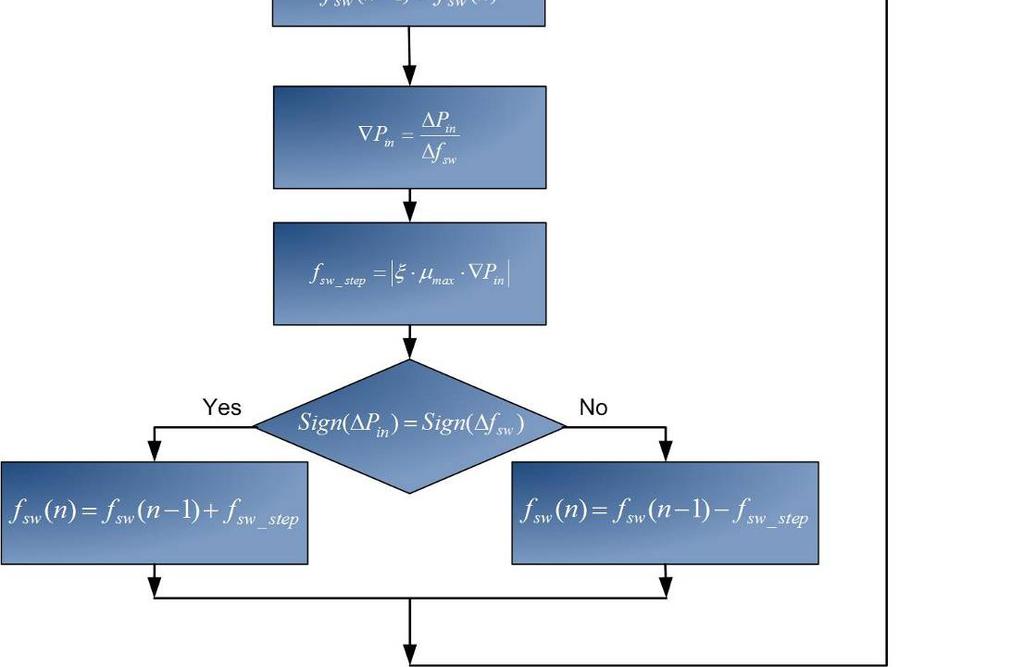
97 Fig. 3.4: Variable-Step-Size (VSS) digital controller flowchart 81
98 3.5 Adaptive Loop Theoretical Design and Guidelines This section describes how the analysis developed in Section 3.3 can be used to design and predict the behavior and stability of the proposed variable step size controller. The design used in this section is the same design used in the experimental work and simulation of the next section. The experimental setup is a single phase DC-DC buck converter with V 12V, in = V = o 1V, Output Inductor: L 400 o = nh, Output Capacitors 5mF, Synchronus FET: NTD40N03R, two in parallel., Control FET: NTD85N02R, two in parallel, FETs Driver: ADI3418K - 12V, The controller is a digital controller implemented in FPGA part: Xilinx Virtex 4, Output Voltage ADC: ADI bit - 30M sample/sec, Input Current ADC: 12-bit 100k sample/sec, and 13-bit DPWM. From the above specs and for 10A load current. The step size for each iteration can be calculated from Equation (3.47). For example, assume that the adaptive loop is at itching frequency of 420 khz and that it converged to this frequency from an initial itching frequency of 455 khz. Using Equation (3.47), the input power gradient can be calculated as follow: First, the average input power P ( n) = 9. 31W at in P in f ( n) = 420kHz and the previous average input power P ( n 1) = 9.41W at in f ( n 1) = 455kHz, the gradient ( n ) can be approximated as: P in I ( ) ( 1) ( ) in n I in n I n = = = in f ( n) f ( n 1) Second, the maximum μ ( n) for any step size can be calculated from Equation (3.31) by taking the derivative of the gradient with respect to the itching frequency as follows: 82
99 (2 ( * d d λ f f )) k = k = 2λ df df From the power stage specs: d k = 2λ = df From Equation (3.43), and to ensure over damped response at the maximum step-size: < μ < μ < μ < λ This value represents the absolute maximum value for μ max above which, the system become unstable. Finally selecting ξ = 0.1 the step size μ( n) is: f = ξμ P = = Hz _ step max in 3.6 Experimental Results To verify the proposed concept, the block diagram of the prototype shown in Fig. 3.1 was built with the specifications presented in Section 3.5. Table 3.1 shows a sample comparison data obtained from the experimental prototype for fixed step-size algorithms and for the proposed adaptive step-size algorithm at different ξ values that affects the convergence speed and the accuracy. Fig. 3.5 shows comparison of the required number of iteration between a fixed step-size algorithm with step size equals to 10 khz and variable step size algorithm at different load currents. Fig. 3.6 shows a comparison of the VSS algorithm itching frequency at different iterations using different zetas at 83
100 different load currents and Fig. 3.7 shows a comparison of the input current resulting from changing the itching frequency at different iterations using different zetas at different load currents. Table 3.1. VSS Experimental Results Fixed Step Size Variable Step Size Load Criteria 5 khz 10 khz 30 khz ξ = 0.05 ξ = 0.1 ξ = 0.15 Exp. Exp. Exp. Exp. Exp. Exp. 5A 10A 15A Iterations % Error Iterations % Error Iterations %Error
101 Switching Freq. (KHz) Fixed Step Size = 10 KHz VSS at Zeta = Number of Iterations Fig. 3.5 (a) Comparing variable step size with fixed step size at 5A load (start up frequency 533 KHz) Switching Freq. (KHz) Fixed Step Size = 10 KHz VSS at Zeta = Number of Iterations Fig. 3.5 (b) Comparing variable step size with fixed step size at 10A load (start up frequency 560 KHz) 85
102 Switching Freq. (KHz) Fixed Step Size = 10 KHz VSS at Zeta = Number of Iterations Fig. 3.5 (c) Comparing variable step size with fixed step size at 15A load (start up frequency 552 KHz) Switching Freq. (KHz) Zeta = 0.05 Zeta = 0.10 Zeta = Number of Iterations Fig. 3.6 (a) Switching frequency at different iterations using different Zetas at 5A load 86
103 Switching Freq. (KHz) Zeta = 0.05 Zeta = 0.10 Zeta = Number of Iterations Fig. 3.6 (b) Switching frequency at different iterations using different Zetas at 10A load Switching Freq. (KHz) Zeta = 0.05 Zeta = 0.10 Zeta = Number of Iterations Fig. 3.6 (c) Switching frequency at different iterations using different Zetas at 15A load 87
104 Input Current (A) Number of Iterations Zeta=0.05 Zeta=0.10 Zeta=0.15 Fig. 3.7 (a): Input current at different iterations using different Zetas at 10A load Input Current (A) Number of Iterations Zeta=0.05 Zeta=0.10 Zeta=0.15 Fig. 3.7 (b): Input current at different iterations using different Zetas at 15A load 88
105 3.7 Conclusion This chapter presents a self auto-tuning algorithm with adaptive variable-step-size to track and detect the optimum itching frequency of DC-DC converter under variable operating conditions such as load variations, voltage variations, components variations, aging effects, and temperature effects. The Variable-Step-Size (VSS) algorithm was theoretically developed and analyzed based on buck DC-DC converter loss model, and a general expression for the gradient function that describes the VSS algorithm was given. The experimental results were compared for both fixed step size algorithm and the adaptive variable step size algorithm. It is shown that the proposed Variable-Step-Size adaptive algorithm achieves better trade off between speed and accuracy compared to the fixed step size algorithm. The convergence stability and speed are analyzed to give the design guidelines for the adaptive loop response. 89
106 CHAPTER FOUR MULTIVARIABLE ADAPTIVE EFFICIENCY OPTIMIZATION DIGITAL CONTROLLER 4.1 Introduction Optimizing the efficiency of DC-DC converters is one of top priorities for power electronics design engineer. Power converter losses, and the corresponding power efficiency for a given design varies at different loading conditions, line conditions, and it is impacted by the variations of temperature and aging effect [27-44]. From studying the power loss in DC-DC converter, it can be noted that there are two main kinds of losses, DC-DC converter itching losses and DC-DC converter conduction losses [31-38]. Switching losses are function of the itching frequency and conduction losses are function of the load current. Optimizing DC-DC converter itching frequency is one way to reduced itching losses [27,31,35]. While optimizing DC-DC converter dead time value can reduce conduction losses [31-38]. The ability of a digital controller to perform sophisticated algorithms makes it easy to apply adaptive control laws where system parameters can be dynamically adjusted in response to system behaviors in order to achieve better efficiency [28]. An adaptive controller and algorithm to optimize itching frequency of DC-DC converter is presented in [27] based on the efficiency tracking concept discussed in [28]. However, the controller in [27] optimizes one parameter only which is the itching frequency while the controller in [28] optimizes another parameter which is the SR dead-time, which may 90
107 not result in maximum or global efficiency point and combined efficiency improvement. Since the input power/current used in both [27] and [28] as the function to minimize, a single controller that optimize both variables at the same time that exhibits multivariable behavior can be used. In this chapter, the analysis, simulation and experimental results for a multivariable adaptive controller (MVAC) that optimize DC-DC converter itching frequency and dead-time together is presented. Next section discusses the effect of itching frequency and dead-time on losses. Section 4.3 presents the multivariable adaptive controller algorithm. Section 4.4 presents a mathematical treatment for the MVAC algorithm stability and sensitivity. Experimental results are discussed in Section 4.5 and finally conclusion is given in Section Effect of Different PWM Parameters on Losses In this section a study of the effect dead-time on total system losses and thus its effect on efficiency is presented. The effect of itching frequency on losses was studied in details in Section 2.2. Fig. 4.1 shows a non-isolated buck DC-DC converter with synchronous rectification to be taken as a converter example to present the MVAC of this chapter. 91
108 Fig. 4.1: Non-isolated synchronous buck DC-DC converter with MVAC controller For synchronous rectifiers there are two main types of dead-time losses: itching losses that depends on the itching frequency and the body diode conduction losses that are function of the load current and body diode forward voltage drop. Dead-Time itching losses occur when turning the MOSFET ON/OFF while its parasitic capacitances are not fully discharged causing hard itching losses. The magnitude of hard itching losses depends on the parasitic capacitance value, the voltage across the capacitance and the itching frequency [29]. The second type of dead-time losses is the body diode conduction losses, which are mainly the result of the MOSFET parasitic diode. When the parasitic capacitance is fully discharged the body diode starts conduction and contributes a conduction loss that depends on the body diode forward voltage drop, and the RMS current passing through it. Finally, the body diode reverse recovery loss is another considerable loss that is generated 92
109 when the body-diode turns off. Reverse recovery losses depends on the charge stored on parasitic capacitor, the voltage across the body diode and the itching frequency [29]. Smaller dead-time means lower MOSFET s body-diode itching and conduction losses. Moreover, the body-diode itching and conduction losses increase with the load. The optimized dead-time that achieves the lowest total body-diode itching and conduction losses is related to many nonlinear parameters that makes the optimized deadtime ( t do ) different at different conditions. An adaptive controller that adaptively adjusts the dead-time, t, within a range depending on such nonlinear parameters variation can d be used to achieve the optimum dead-time t do. Fig. 4.2 shows that at given load condition there exist an optimized dead-time value where the efficiency is maximum. (a) 93
110 (b) (c) Fig. 4.2: Efficiency vs. Dead-Time at (a) 0.1A, (b) 1.0A and (c) 6.0A. At different loads there is an optimized Dead-Time value at which the efficiency is maximum. 94
111 From the above discussion, it can be noted that there is an optimized itching frequency, dead-time value for each load where the itching and conduction losses are minimum [31]. Fig. 4.3 shows a three dimensional surface plot for frequency, dead-time and efficiency at different load conditions for a typical synchronous buck DC-DC converter design. Fig. 4.3 surface plots are obtained from a comprehensive multivariable loss model built in MathCad. From Fig. 4.3 it can be noted that for each load there is an optimum (frequency, dead-time) pair points where efficiency is maximum. The multivariable controller presented in the next section aims at finding the optimum pair for frequency and dead-time at variable loads and other conditions. 95
 3D surface plot for the itching frequency, dead-time and efficiency")
: Contour plot for")
112 Fig. 4.3: (a) 3D surface plot for the itching frequency, dead-time and efficiency at load current = 0.1A, optimum F = 50 khz, optimum Dead-Time = 80ns Fig. 4.3 (b): Contour plot for the itching frequency, dead-time and efficiency at load current = 0.1A, optimum F = 50 khz, optimum dead-time = 80ns 96
: 3D surface plot for the itching frequency, dead-time and efficiency")
: Contour plot for")
113 Fig. 4.3 (c): 3D surface plot for the itching frequency, dead-time and efficiency at load current = 1.0A, optimum F = 100 khz, optimum dead-time = 60ns Fig. 4.3 (d): Contour plot for the itching frequency, dead-time and efficiency at load current = 1.0A, optimum F = 100 khz, optimum dead-time = 60ns 97
: 3D surface plot for the itching frequency, dead-time and efficiency")
: Contour plot for")
114 Fig. 4.3 (e): 3D surface plot for the itching frequency, dead-time and efficiency at load current = 6.0A, optimum F = 150 khz, optimum dead-time = 40ns Fig. 4.3 (f): Contour plot for the itching frequency, dead-time and efficiency at load current = 6.0A, optimum F = 150 khz, optimum Dead-Time = 40ns 98
115 4.3 Multivariable Adaptive Digital Controller Fig. 4.4 shows an implementation flowchart for the Multivariable adaptive controller algorithm. From the flowchart, N samples of (converter sensed input power) using the ADC and are stored and averaged to generate P ( n). P ( n) is used as an indication of the converter efficiency since the maximum efficiency point occurs at the P in in in minimum input power point. P in is used at a later stage to decide the value of the digital controller itching frequency and dead-time values. Next, the Multivariable Adaptive Controller (MVAC) starts optimizing the itching frequency as shown in Fig Switching frequency optimization starts by calculating the difference between the previous value and the new value of P in and the difference between the current value and the previous value of f as follows: Δ P = P ( n) P ( n 1) in in in (4.1) Δ f = f ( n) f ( n 1) (4.2) After that, a sign comparison between ΔP in and Δ f is made. If the signs (positive or negative) of Equations (4.1) and (4.2) are similar, this means f should be incremented by f _ step to move toward the maximum efficiency point (or minimum 99
116 input power). Otherwise, if the signs of Equations (4.1) and (4.2) are not similar, this means f should be decremented by f _ step to move toward the maximum efficiency point. Increasing the converter efficiency by decreasing the input power indicates a reduction in the total losses to the minimum possible value (optimal itching frequency value). After storing the current values of P in and f, the program will decrement or increment f and update it. Then, after several ( M ) itching cycles (enough to reach steady-state), P in is sampled again and the MVAC algorithm starts optimizing the Dead- Time. Dead-Time optimization is done in a similar way to the frequency optimization; first the difference between the previous value and the new value of P in is found, then the difference between the current value and the previous value of d t is calculated as follows: Δ d t = d t ( n) d t ( n 1) (4.3) After that, a sign comparison between Pin and dt Δ Δ is made. If the signs (positive or negative) of Equations (4.1) and (4.3) are similar, this means d t should be incremented by d t _ step to move toward the maximum efficiency point (or minimum input power). Otherwise, if the signs of Equations (4.1) and (4.3) are not similar, this means d t should be decremented by d t _ step to move toward the maximum efficiency point. Increasing the converter efficiency by decreasing the input power indicates a reduction in the total losses 100
117 to the minimum value (optimal dead-time value). After storing the current values of P in and d, the program will decrement or increment d and update it. Then, after several ( M ) t itching cycles (enough to reach steady-state) MVAC algorithm starts optimizing the itching frequency again. The MVAC keep optimizing the itching frequency and the dead-time one step at a time till the global maximum efficiency point is reached. t It must be noted that the compensated control signal D c that regulates the converter output voltage is generated by a digital controller that also contains the MVAC algorithm. In addition, the MVAC loop bandwidth is much smaller than the output voltage regulation loop bandwidth. Finally it should be noted that the performance curve has a global maximum with respect to the controlling parameter [27,28], consequently the initial values of the controlling parameters and the strategy used in adjusting the parameter will not affect the convergence to the global maximum efficiency. 101

118 Fig. 4.4: Multivariable adaptive controller (MVAC) flowcharts 102
119 4.4 The MVAC Algorithm and its Analysis Determining the stability and sensitivity for adaptive systems is of great importance since it determines the stable region of operation for the adaptive controller. Multivariable adaptive controller adaptively perturbs DC-DC converter itching frequency and the dead-time to track the optimum system efficiency. In this section theoretical analysis for the stability and sensitivity for multivariable adaptive controller applied to synchronous buck DC-DC converter is discussed and analyzed. The stability and sensitivity analysis for frequency perturbation was discussed in details in Section 2.3.1, the following analysis focus on stability and sensitivity for dead-time perturbation Adaptive Dead-Time Optimization The input power is to be used as a cost function to track the maximum efficiency. Fig. 4.5 shows the input power resulting from perturbing the dead-time. The curve is continuous with one local minimum. It can be noted also from the curve that the minimum input power corresponds to the maximum efficiency. Approximating input current curve as a parabola, which can be represented in Equation (4.4) [64]: P = P _min + λ ( d d ) * 2 in in t t (4.4) where is the input power which is the cost function to be minimized, is the P in P in _min * minimum input power, is the dead-time, is the optimum dead-time that gives the d t d t 103
120 minimum input power. λ is proportionality constant. Taking the first derivative of Equation (4.4): dpin dd ( ) t = * 2 λ ( dt dt ) (4.5) Fig. 4.5 Input current as function of dead-time The second derivative is a constant value over the entire input current curve: 2 dpin = 2 2 ( t ) dd λ (4.6) 104
121 The main goal of the analysis is to find the optimum dead-time value * d t that minimizes the input power/current to its lowest value. At different loads and system parameters the exact input power/current curve is not known, so a search algorithm to find the optimum point is needed. The search algorithm starts with an initial value for the deadtime d t0, then measures the slope of the input power curve at that point. Next the algorithm calculates a new dead-time value d t1, which equals to the old dead-time plus/minus an incremental value. The iterative process repeats until the optimum deadtime * d t is found Gradient Search Using Steepest Descent Method There are many algorithms used for gradients search, a simple and practical one is the steepest descent algorithm. This algorithm follows the search method described above and can be represented by Equation (4.7) as [64] : d = d + μ ( ) t k+ 1 t k k (4.7) where k is the iteration number, d + is the new dead-time value, is the present dead- t k 1 d tk time value, μ is a constant that controls stability and convergence of the adaptive loop and k is the gradient of the cost function at dt =, using equation (4.5) the gradient d t k k can be expressed as : 105
122 dp in * k = = 2 λ ( t k t ) dd ( t ) d = d t t k d d (4.8) The steepest descent adaptive loop dynamics from the initial dead-time iteration d t 0 to the optimum dead-time value * d t can be studied by substituting equation (4.8) into equation (4.7) as [64]: d = d 2 μλ ( d d * t t t t k+ 1 k k ) (4.9) Rearranging the equation: d t k+ 1 = (1 2 μλ) d + 2μλ t k * d t (4.10) Taking the first four iterations of (4.10) gives d t = (1 2 μλ) dt + 2μλ d t 1 0 * (4.11) d d d 2 0 [ ] 2 * t = (1 2 μλ) t + 2 μλ t (1 2 μλ) + 1 (4.12) d d d 3 * 2 t = (1 2 μλ) t + 2 μλ t (1 2 μλ) + (1 2 μλ) (4.13) 106
123 d d d 4 * 3 2 t = (1 2 μλ) t + 2 μλ t (1 2 μλ) + (1 2 μλ) + (1 2 μλ) From those equations, a general expression for d tk at any iteration can be given as [64]: (4.14) k 1 k * tk t0 t n= 0 d = (1 2 μλ) d + 2 μλ d (1 2 μλ) n (4.15) k k * 1 (1 2 μλ) dt = (1 2 μλ) d 2 k t + μλ d 0 t 1 (1 2 μλ) (4.16) d = d + (1 2 μλ) ( d d ) * k * t t t t k 0 (4.17) Gradient Stability and Convergence The ratio between successive terms in the summation in equation (4.17) can be defined as r = 1 2μλ, the ratio r is the most important parameter that determine the stability of the adaptive loop. From equation (4.17) it is clear that the iterative process will be stable if r = 1 2μλ < 1 (4.18) 107
124 This condition can be expressed also as [64] 1 μ 0 λ > > (4.19) If the condition in equation (4.18) or (4.19) is satisfied, the adaptive loop will be stable and will converge to the optimum dead time value [64]: lim dt k = d k * t (4.20) It can be noted also that the ratio r plays an important role in determining the convergence speed to the optimum solution. Fig. 4.6 shows weight adjustment behavior for the dead-time adaptive loop at different values of r, the adaptive loop starts with initial dead-time of 200ns and tries to reach the optimum dead-time of 50ns. From the figure, it can be noted that the rate of convergence increase as r value decrease reach to its maximum at r=0. Also it can be noted that for positive values of r (Overdamped) there is no oscillation while for negative values (Underdamped) there is an overshoot which decays eventually to the optimum point. Finally at r=0 the system is called critically damped which theoretically yields the fastest convergence [64]. 108
125 Fig. 4.6 Weight adjustment behavior for dead-time adaptive loop at different values of r Adaptive Dead-Time Sensitivity Analysis The sensitivity of the input power P in (or input current assuming the input voltage is either constant or slow changing) to a change in dead-time normalized change in P over the normalized change in d : in t d t can be defined as the S Pin dt ΔP in P in ΔP in dt = = Δdt Δdt P in dt (4.21) 109
126 For MVAC process, where the dead-time sensitivity can be approximated as: dt is changing in successive iterations, the S P d = Pin in t dt dt Pin (4.22) Equation (4.22) can also be defined as: d Pin t Sd = P t in P in The expression for the input current gradient function Iin can be found as follows: P = P + P = V I + ( P + P + P ) in out Losses out out Conduction Switching DeadTime (4.23) Yielding, (4.24) P V I P P P P Pin = = = d d d d d d in out out Conduction Switching DeadTime DeadTime t t t t t t Dead-Time losses can be approximated by PDeadTime = dt f VD Iout (4.25) (4.26) 110
127 This mean the input power gradient for perturbation in dead-time is: P P d f V I P = = = = f V I in DeadTime t D out in D out dt dt dt (4.27) Substituting equation (4.27) into equation (4.23), the input power sensitivity due to perturbation in dead-time is give by: d f V I d P t D out t in Sd = Pin = t I I in in (4.28) It should be noted that for the sake of simplicity the first order equation in (4.26) was used to derive the sensitivity analysis. Future research will include deriving a more exact relation which has the 2 nd order dependency as in equation (4.4). 4.5 Experimental Results The MVAC method was prototyped using a digital microcontroller. The experimental power stage is a single phase synchronous buck DC-DC converter with Vin Lo,, input capacitors = 10V V = 3.3V 940μ F o,output capacitors 991μ F, output Inductor: = 2.6μH with DCR = 1mΩ, upper FET: IRFR5305 [60], two in parallel, lower FET: IRFR2905 [61], two in parallel, and TC428COA FET Driver [62]. The digital microcontroller is used to implement both the MVAC and the output voltage regulation closed loop. The experimental setup uses three 12-bit ADC s with maximum input voltage 111
128 of 3.3V to convert the measured parameters. One ADC is used to convert the sensed output voltage; the converted output voltage data is used at a later stage by a digital PID compensator to regulate the output voltage. The second and third ADC s are used for input current sensing and input voltage sensing respectively; the converted data is then processed by the digital controller and utilized by the MVAC algorithm. The synchronous buck converter was designed to be able to itch between CCM and DCM modes of operation depending on the load using the scheme described in AFO experimental result section 1.6. Fig. 4.7 shows the efficiency versus itching frequency curves obtained from the experimental setup at different loading currents where the itching frequency is varied within a range at each given load. Fig. 4.7 (a): Experimental efficiency vs. itching frequency at 0.6A load at DCM mode. 112
129 Fig. 4.7 (b): Experimental efficiency vs. itching frequency at 0.8A load at DCM mode. Fig. 4.7 (c): Experimental efficiency vs. itching frequency at 1.0A load at DCM mode. 113
130 Fig. 4.7 (d): Experimental efficiency vs. itching frequency at different loads at CCM mode. Fig. 4.8 shows the efficiency versus dead-time curves obtained from the same experimental setup at different loading currents where the dead-time is varied within a range at each given load. From Fig. 4.8, it is clear again that for each load there is an optimized Dead-Time value at which the total itching and conduction losses are minimum and thus efficiency is maximum. It can be noted also from Fig. 4.8 that as the load current increase the optimum Dead-Time value decreased as discussed in section 4.2 dead time effect on losses. 114
131 Fig. 4.8 (a): Experimental efficiency vs. dead-time at 0.1A load at DCM mode. Fig. 4.8 (b): Experimental efficiency vs. dead-time at 1.0A load at DCM mode. 115
132 Fig. 4.8 (c): Experimental efficiency vs. dead-time at 6.0A load at CCM mode. Fig. 4.8 (d): Experimental efficiency vs. dead-time at 8.0A load at CCM mode. 116
133 Fig. 4.9 shows a comparison between efficiency improvements resulted from fixed itching frequency with CCM/DCM enabled versus Adaptive Frequency Optimization (AFO) algorithm versus the new Multivariable Adaptive Controller (MVAC) algorithm, as can be noted from the figures, Multivariable adaptive efficiency optimization (MVAC) achieves the highest efficiency improvement compared to AFO or the fixed frequency approach. Fig. 4.9 (a): Efficiency comparison between different schemes working at Vin=10V. 117
134 Fig. 4.9 (b): Efficiency comparison between different schemes working at Vin=12V. Fig. 4.9 (c): Efficiency comparison between different schemes working at Vin=8V. 118
135 Table 4.1 shows efficiency comparison at different input voltages. It can be noticed from Table 4.1 how MVAC controller detects the new optimum (itching frequency, Dead-Time) values and adjusts both variables when the input voltage varies from 8V to 10V to 12V. As the input voltage increases, the optimum (itching frequency Dead-Time) values may be lower or higher depending on the trade off between conduction losses and itching losses. Table 4.1: Optimum itching frequency and Dead-Time and the resulted efficiency at different input voltages and different load currents Vin 8.0V 10.0V 12.0V Load f optimum Dt optimum Eff f optimum Dt optimum Eff f optimum Dt optimum (khz) (ns ) (%) (khz) (ns ) (%) (khz) (ns ) Eff (%) 0.1A A A A Finally, Fig shows how the MVAC algorithm moves toward the optimum itching frequency and Dead-Time values in different loading conditions. In Fig 4.10 (a) and the related contour plot 4.10 (b) the MVAC algorithm tries to find the optimum operating points for 1A load current working at 12V input voltage. The algorithm starts with itching frequency of 50 khz and Dead-Time value of 150ns. MVAC iterates 10 times with itching frequency step size of 10 khz and Dead-Time step size of 20ns to 119
136 reach the optimum points of itching frequency of 100 khz and Dead-Time value of 60ns. After finding the optimum working points, the algorithm keep moving between two or more points around the optimum values as shown in Fig (a) which shows number iteration vs. itching frequency and Fig (b) which shows number of iteration vs. the Dead-Time value. 120
: 3D surface plot that shows how the MVAC algorithm approaches the")
: Contour plot that shows how the MVAC algorithm approaches the 121")
137 Fig (a): 3D surface plot that shows how the MVAC algorithm approaches the optimum efficiency point (f_opt = 100 khz, Dt_opt=60ns) for 1.0A load current. Fig (b): Contour plot that shows how the MVAC algorithm approaches the optimum efficiency point (f_opt = 100 khz, Dt_opt=60ns) for 1.0A load current. 121
138 Fig.4.11 (a): Iteration vs. itching frequency for 1.0A load current example. Fig.4.11 (b): Iteration vs. dead-time for 1.0A load current example 122
139 In Fig 4.12 (a) and 4.12 (b) the MVAC algorithm tries to find the optimum operating points for 4A load current working at 12V input voltage. The algorithm starts with itching frequency of 300 khz and Dead-Time value of 10ns. MVAC iterates 22 times with itching frequency step size of 10 khz and Dead-Time step size of 20ns to reach the optimum points of itching frequency of 190 khz and Dead-Time value of 50ns. After finding the optimum working points, the algorithm keep moving between two or more points around the optimum values as shown in Fig (a) which shows number iteration vs. itching frequency and Fig (b) which shows number of iteration vs. the Dead-Time value. 123
: 3D surface plot that shows how the MVAC algorithm approaches the")
: Contour plot that shows how the MVAC algorithm approaches the 124")
140 Fig (a): 3D surface plot that shows how the MVAC algorithm approaches the optimum efficiency point (f_opt = 190 khz, Dt_opt=50ns) for 4.0A load current. Fig (b): Contour plot that shows how the MVAC algorithm approaches the optimum efficiency point (f_opt = 190 khz, Dt_opt=50ns) for 4.0A load current. 124
Chapter 3 : Closed Loop Current Mode DC\DC Boost Converter
 Chapter 3 : Closed Loop Current Mode DC\DC Boost Converter 3.1 Introduction DC/DC Converter efficiently converts unregulated DC voltage to a regulated DC voltage with better efficiency and high power density.
CONTENTS. Chapter 1. Introduction to Power Conversion 1. Basso_FM.qxd 11/20/07 8:39 PM Page v. Foreword xiii Preface xv Nomenclature
 Basso_FM.qxd 11/20/07 8:39 PM Page v Foreword xiii Preface xv Nomenclature xvii Chapter 1. Introduction to Power Conversion 1 1.1. Do You Really Need to Simulate? / 1 1.2. What You Will Find in the Following
Digital PWM IC Control Technology and Issues
 Digital PWM IC Control Technology and Issues Prof. Seth R. Sanders Angel V. Peterchev Jinwen Xiao Jianhui Zhang Department of EECS University of California, Berkeley Digital Control Advantages implement
Alternated duty cycle control method for half-bridge DC-DC converter
 HAIT Journal of Science and Engineering B, Volume 2, Issues 5-6, pp. 581-593 Copyright C 2005 Holon Academic Institute of Technology CHAPTER 3. CONTROL IN POWER ELEC- TRONIC CIRCUITS Alternated duty cycle
ADAPTIVE CONTROL METHODS FOR DC-DC SWITCHING POWER CONVERTERS VARAPRASAD ARIKATLA
 ADAPTIVE CONTROL METHODS FOR DC-DC SWITCHING POWER CONVERTERS by VARAPRASAD ARIKATLA JABER ABU QAHOUQ, COMMITTEE CHAIR TIM A. HASKEW YANG-KI HONG JEFF JACKSON DANIEL J. FONSECA A DISSERTATION Submitted
Conventional And Zvt Synchronous Buck Converter Design, Analysis, And Measurement
 University of Central Florida Electronic Theses and Dissertations Masters Thesis (Open Access) Conventional And Zvt Synchronous Buck Converter Design, Analysis, And Measurement 2010 Mark Cory University
CHAPTER 3 APPLICATION OF THE CIRCUIT MODEL FOR PHOTOVOLTAIC ENERGY CONVERSION SYSTEM
 63 CHAPTER 3 APPLICATION OF THE CIRCUIT MODEL FOR PHOTOVOLTAIC ENERGY CONVERSION SYSTEM 3.1 INTRODUCTION The power output of the PV module varies with the irradiation and the temperature and the output
Maximum Power Extraction from A Small Wind Turbine Using 4-phase Interleaved Boost Converter
 Maximum Power Extraction from A Small Wind Turbine Using 4-phase Interleaved Boost Converter Liqin Ni Email: liqin.ni@huskers.unl.edu Dean J. Patterson Email: patterson@ieee.org Jerry L. Hudgins Email:
TABLE OF CONTENTS CHAPTER NO. TITLE PAGE NO. LIST OF TABLES LIST OF FIGURES LIST OF SYMBOLS AND ABBREVIATIONS
 vi TABLE OF CONTENTS CHAPTER NO. TITLE PAGE NO. ABSTRACT LIST OF TABLES LIST OF FIGURES LIST OF SYMBOLS AND ABBREVIATIONS iii x xi xvii 1 INTRODUCTION 1 1.1 INTRODUCTION 1 1.2 BACKGROUND 2 1.2.1 Types
AN726. Vishay Siliconix AN726 Design High Frequency, Higher Power Converters With Si9166
 AN726 Design High Frequency, Higher Power Converters With Si9166 by Kin Shum INTRODUCTION The Si9166 is a controller IC designed for dc-to-dc conversion applications with 2.7- to 6- input voltage. Like
Fundamentals of Power Electronics
 Fundamentals of Power Electronics SECOND EDITION Robert W. Erickson Dragan Maksimovic University of Colorado Boulder, Colorado Preface 1 Introduction 1 1.1 Introduction to Power Processing 1 1.2 Several
Digital Control Techniques for Efficiency Improvements in Single-Phase Boost Power Factor Correction Rectifiers
 University of Colorado, Boulder CU Scholar Electrical, Computer & Energy Engineering Graduate Theses & Dissertations Electrical, Computer & Energy Engineering Spring 1-1-2010 Digital Control Techniques
Improvement of SBC Circuit using MPPT Controller
 Improvement of SBC Circuit using MPPT Controller NOR ZAIHAR YAHAYA & AHMAD AFIFI ZAMIR Electrical & Electronic Engineering Department Universiti Teknologi PETRONAS Bandar Seri Iskandar, 3750 Tronoh, Perak
Digital Control Technologies for Switching Power Converters
 Digital Control Technologies for Switching Power Converters April 3, 2012 Dr. Yan-Fei Liu, Professor Department of Electrical and Computer Engineering Queen s University, Kingston, ON, Canada yanfei.liu@queensu.ca
Vishay Siliconix AN724 Designing A High-Frequency, Self-Resonant Reset Forward DC/DC For Telecom Using Si9118/9 PWM/PSM Controller.
 AN724 Designing A High-Frequency, Self-Resonant Reset Forward DC/DC For Telecom Using Si9118/9 PWM/PSM Controller by Thong Huynh FEATURES Fixed Telecom Input Voltage Range: 30 V to 80 V 5-V Output Voltage,
ENTIRE LOAD EFFICIENCY AND DYNAMIC PERFORMANCE IMPROVEMENTS FOR DC-DC CONVERTERS
 ENTIRE LOAD EFFICIENCY AND DYNAMIC PERFORMANCE IMPROVEMENTS FOR DC-DC CONVERTERS by OSAMA A. ABDEL-RAHMAN B.S. Princess Sumaya University for Technology, 2003 M.S. University of Central Florida, 2005 A
A New Small-Signal Model for Current-Mode Control Raymond B. Ridley
 A New Small-Signal Model for Current-Mode Control Raymond B. Ridley Copyright 1999 Ridley Engineering, Inc. A New Small-Signal Model for Current-Mode Control By Raymond B. Ridley Before this book was written
Conventional Single-Switch Forward Converter Design
 Maxim > Design Support > Technical Documents > Application Notes > Amplifier and Comparator Circuits > APP 3983 Maxim > Design Support > Technical Documents > Application Notes > Power-Supply Circuits
ACT111A. 4.8V to 30V Input, 1.5A LED Driver with Dimming Control GENERAL DESCRIPTION FEATURES APPLICATIONS TYPICAL APPLICATION CIRCUIT
 4.8V to 30V Input, 1.5A LED Driver with Dimming Control FEATURES Up to 92% Efficiency Wide 4.8V to 30V Input Voltage Range 100mV Low Feedback Voltage 1.5A High Output Capacity PWM Dimming 10kHz Maximum
DC/DC Converters for High Conversion Ratio Applications
 DC/DC Converters for High Conversion Ratio Applications A comparative study of alternative non-isolated DC/DC converter topologies for high conversion ratio applications Master s thesis in Electrical Power
FEATURES DESCRIPTION APPLICATIONS PACKAGE REFERENCE
 DESCRIPTION The is a monolithic synchronous buck regulator. The device integrates 100mΩ MOSFETS that provide 2A continuous load current over a wide operating input voltage of 4.75V to 25V. Current mode
A7221A DC-DC CONVERTER/BUCK (STEP-DOWN) 600KHz, 16V, 2A SYNCHRONOUS STEP-DOWN CONVERTER
 600KHz, 16V, 2A SYNCHRONOUS STEP-DOWN CONVERTER") DESCRIPTION The is a fully integrated, high efficiency 2A synchronous rectified step-down converter. The operates at high efficiency over a wide output current load range. This device offers two operation
DESCRIPTION The is a fully integrated, high efficiency 2A synchronous rectified step-down converter. The operates at high efficiency over a wide output current load range. This device offers two operation
Chapter 2 Buck PWM DC DC Converter
 Chapter 2 Buck PWM DC DC Converter H. Wang, Power Management and High-speed I/O in CMOS Systems 1/25 Buck Circuit and Its equivalent circuits CCM: continuous conduction mode DCM: discontinuous conduction
Methodology for testing a regulator in a DC/DC Buck Converter using Bode 100 and SpCard
 Methodology for testing a regulator in a DC/DC Buck Converter using Bode 100 and SpCard J. M. Molina. Abstract Power Electronic Engineers spend a lot of time designing their controls, nevertheless they
Switched Mode Power Conversion Prof. L. Umanand Department of Electronics Systems Engineering Indian Institute of Science, Bangalore
 Switched Mode Power Conversion Prof. L. Umanand Department of Electronics Systems Engineering Indian Institute of Science, Bangalore Lecture -1 Introduction to DC-DC converter Good day to all of you, we
DESCRIPTION FEATURES APPLICATIONS TYPICAL APPLICATION. 500KHz, 18V, 2A Synchronous Step-Down Converter
 DESCRIPTION The is a fully integrated, high-efficiency 2A synchronous rectified step-down converter. The operates at high efficiency over a wide output current load range. This device offers two operation
Impact of the Flying Capacitor on the Boost converter
 mpact of the Flying Capacitor on the Boost converter Diego Serrano, Víctor Cordón, Miroslav Vasić, Pedro Alou, Jesús A. Oliver, José A. Cobos Universidad Politécnica de Madrid, Centro de Electrónica ndustrial
High Accurate non-isolated Buck LED Driver
 High Accurate non-isolated Buck LED Driver Features High efficiency (More than 90%) High precision output current regulation (-3%~+3%) when universal AC input voltage (85VAC~265VAC) Lowest cost and very
MP1482 2A, 18V Synchronous Rectified Step-Down Converter
 The Future of Analog IC Technology MY MP48 A, 8 Synchronous Rectified Step-Down Converter DESCRIPTION The MP48 is a monolithic synchronous buck regulator. The device integrates two 30mΩ MOSFETs, and provides
600KHz, 16V/2A Synchronous Step-down Converter
 600KHz, 16V/2A Synchronous Step-down Converter General Description The contains an independent 600KHz constant frequency, current mode, PWM step-down converters. The converter integrates a main switch
HM8113B. 3A,4.5V-16V Input,500kHz Synchronous Step-Down Converter FEATURES GENERAL DESCRIPTION APPLICATIONS TYPICAL APPLICATION
 3A,4.5-16 Input,500kHz Synchronous Step-Down Converter FEATURES High Efficiency: Up to 96% 500KHz Frequency Operation 3A Output Current No Schottky Diode Required 4.5 to 16 Input oltage Range 0.6 Reference
Integrated Power Electronic Converters and Digital Control
 Integrated Power Electronic Converters and Digital Control Ali Emadi * Alireza Khaligh Zhong Nie Young Joo Lee Q\ CRC Press / Taylor &.Francis Group Boca Raton London New York CRC Press is an imprint of
DESIGN AND FPGA IMPLEMENTATION OF SLIDING MODE CONTROLLER FOR BUCK CONVERTER
 DESIGN AND FPGA IMPLEMENTATION OF SLIDING MODE CONTROLLER FOR BUCK CONVERTER 1 ABHINAV PRABHU, 2 SHUBHA RAO K 1 Student (M.Tech in CAID), 2 Associate Professor Department of Electrical and Electronics,
CHAPTER 3 MAXIMUM POWER TRANSFER THEOREM BASED MPPT FOR STANDALONE PV SYSTEM
 60 CHAPTER 3 MAXIMUM POWER TRANSFER THEOREM BASED MPPT FOR STANDALONE PV SYSTEM 3.1 INTRODUCTION Literature reports voluminous research to improve the PV power system efficiency through material development,
SINGLE-STAGE HIGH-POWER-FACTOR SELF-OSCILLATING ELECTRONIC BALLAST FOR FLUORESCENT LAMPS WITH SOFT START
 SINGLE-STAGE HIGH-POWER-FACTOR SELF-OSCILLATING ELECTRONIC BALLAST FOR FLUORESCENT S WITH SOFT START Abstract: In this paper a new solution to implement and control a single-stage electronic ballast based
The Technology Behind the World s Smallest 12V, 10A Voltage Regulator
 The Technology Behind the World s Smallest 12V, 10A Voltage Regulator A low profile voltage regulator achieving high power density and performance using a hybrid dc-dc converter topology Pradeep Shenoy,
4.5V to 32V Input High Current LED Driver IC For Buck or Buck-Boost Topology CN5816. Features: SHDN COMP OVP CSP CSN
 4.5V to 32V Input High Current LED Driver IC For Buck or Buck-Boost Topology CN5816 General Description: The CN5816 is a current mode fixed-frequency PWM controller for high current LED applications. The
Digital PWM IC Control Technology and Issues
 Digital PWM IC Control Technology and Issues Prof. Seth R. Sanders (sanders@eecs.berkeley.edu) Angel V. Peterchev Jinwen Xiao Jianhui Zhang EECS Department University of California, Berkeley Digital Control
DESCRIPTION FEATURES PROTECTION FEATURES APPLICATIONS. RS2320 High Accurate Non-Isolated Buck LED Driver
 High Accurate Non-Isolated Buck LED Driver DESCRIPTION RS2320 is especially designed for non-isolated LED driver. The building in perfect current compensation function ensures the accurate output current.
Steady State And Dynamic Analysis And Optimization Of Single-stage Power Factor Correction Converters
 University of Central Florida Electronic Theses and Dissertations Doctoral Dissertation (Open Access) Steady State And Dynamic Analysis And Optimization Of Single-stage Power Factor Correction Converters
MP2305 2A, 23V Synchronous Rectified Step-Down Converter
 The Future of Analog IC Technology MP305 A, 3 Synchronous Rectified Step-Down Converter DESCRIPTION The MP305 is a monolithic synchronous buck regulator. The device integrates 30mΩ MOSFETS that provide
1.5MHz, 800mA, High-Efficiency PWM Synchronous Step-Down Converter
 1.5MHz, 800mA, High-Efficiency PWM Synchronous Step-Down Converter Description The is a high efficiency, low-noise, DC-DC step-down pulse width modulated (PWM) converter that goes automatically into PFM
Designing A High-Frequency, Higher-Power Buck/Boost Converter for Multi-Cell Input Configurations Using Si9168
 AN79 Designing A High-Frequency, Higher-Power Buck/Boost Converter for Multi-Cell Input Configurations Using Si968 Nitin Kalje The Si968 is a high-frequency synchronous dc-to-dc controller designed for
2A,4.5V-21V Input,500kHz Synchronous Step-Down Converter FEATURES GENERAL DESCRIPTION APPLICATIONS TYPICAL APPLICATION
 2A,4.5-21 Input,500kHz Synchronous Step-Down Converter FEATURES High Efficiency: Up to 96% 500KHz Frequency Operation 2A Output Current No Schottky Diode Required 4.5 to 21 Input oltage Range 0.8 Reference
I. INTRODUCTION II. LITERATURE REVIEW
 ISSN XXXX XXXX 2017 IJESC Research Article Volume 7 Issue No.11 Non-Isolated Voltage Quadrupler DC-DC Converter with Low Switching Voltage Stress Praveen Kumar Darur 1, Nandem Sandeep Kumar 2, Dr.P.V.N.Prasad
WD3122EC. Descriptions. Features. Applications. Order information. High Efficiency, 28 LEDS White LED Driver. Product specification
 High Efficiency, 28 LEDS White LED Driver Descriptions The is a constant current, high efficiency LED driver. Internal MOSFET can drive up to 10 white LEDs in series and 3S9P LEDs with minimum 1.1A current
idesyn id8802 2A, 23V, Synchronous Step-Down DC/DC
 2A, 23V, Synchronous Step-Down DC/DC General Description Applications The id8802 is a 340kHz fixed frequency PWM synchronous step-down regulator. The id8802 is operated from 4.5V to 23V, the generated
Engineer-to-Engineer Note
 Engineer-to-Engineer Note EE-339 a Technical notes on using Analog Devices DSPs, processors and development tools Visit our Web resources http://www.analog.com/ee-notes and http://www.analog.com/processors
R. W. Erickson. Department of Electrical, Computer, and Energy Engineering University of Colorado, Boulder
 R. W. Erickson Department of Electrical, Computer, and Energy Engineering University of Colorado, Boulder 6.3.5. Boost-derived isolated converters A wide variety of boost-derived isolated dc-dc converters
ANALOG-TO-DIGITAL CONVERTER FOR INPUT VOLTAGE MEASUREMENTS IN LOW- POWER DIGITALLY CONTROLLED SWITCH-MODE POWER SUPPLY CONVERTERS
 ANALOG-TO-DIGITAL CONVERTER FOR INPUT VOLTAGE MEASUREMENTS IN LOW- POWER DIGITALLY CONTROLLED SWITCH-MODE POWER SUPPLY CONVERTERS Aleksandar Radić, S. M. Ahsanuzzaman, Amir Parayandeh, and Aleksandar Prodić
A Control Scheme for an AC-DC Single-Stage Buck-Boost PFC Converter with Improved Output Ripple Reduction
 Western University Scholarship@Western Electronic Thesis and Dissertation Repository August 2012 A Control Scheme for an AC-DC Single-Stage Buck-Boost PFC Converter with Improved Output Ripple Reduction
Increasing Performance Requirements and Tightening Cost Constraints
 Maxim > Design Support > Technical Documents > Application Notes > Power-Supply Circuits > APP 3767 Keywords: Intel, AMD, CPU, current balancing, voltage positioning APPLICATION NOTE 3767 Meeting the Challenges
Features MIC2193BM. Si9803 ( 2) 6.3V ( 2) VDD OUTP COMP OUTN. Si9804 ( 2) Adjustable Output Synchronous Buck Converter
 6.3V ( 2) VDD OUTP COMP OUTN. Si9804 ( 2) Adjustable Output Synchronous Buck Converter") MIC2193 4kHz SO-8 Synchronous Buck Control IC General Description s MIC2193 is a high efficiency, PWM synchronous buck control IC housed in the SO-8 package. Its 2.9V to 14V input voltage range allows
MIC2193 4kHz SO-8 Synchronous Buck Control IC General Description s MIC2193 is a high efficiency, PWM synchronous buck control IC housed in the SO-8 package. Its 2.9V to 14V input voltage range allows
AN294. Si825X FREQUENCY COMPENSATION SIMULATOR FOR D IGITAL BUCK CONVERTERS
 Si825X FREQUENCY COMPENSATION SIMULATOR FOR D IGITAL BUCK CONVERTERS Relevant Devices This application note applies to the Si8250/1/2 Digital Power Controller and Silicon Laboratories Single-phase POL
Analysis and comparison of two high-gain interleaved coupled-inductor boost converters
 Scholars' Mine Masters Theses Student Research & Creative Works 2015 Analysis and comparison of two high-gain interleaved coupled-inductor boost converters Venkat Sai Prasad Gouribhatla Follow this and
APPLICATION NOTE 6071 CHOOSE THE RIGHT REGULATOR FOR THE RIGHT JOB: PART 3, COMPONENT SELECTION
 Keywords: Switching Regulators,Step Down,Inductors,Simulation,EE-Sim,component selection APPLICATION NOTE 6071 CHOOSE THE RIGHT REGULATOR FOR THE RIGHT JOB: PART 3, COMPONENT SELECTION By: Don Corey, Principal
3A, 23V, 380KHz Step-Down Converter
 3A, 23V, 380KHz Step-Down Converter General Description The is a buck regulator with a built in internal power MOSFET. It achieves 3A continuous output current over a wide input supply range with excellent
Analysis and loss estimation of different multilevel DC-DC converter modules and different proposed multilevel DC-DC converter systems
 The University of Toledo The University of Toledo Digital Repository Theses and Dissertations 2014 Analysis and loss estimation of different multilevel DC-DC converter modules and different proposed multilevel
Analog Technologies. ATI2202 Step-Down DC/DC Converter ATI2202. Fixed Frequency: 340 khz
 Step-Down DC/DC Converter Fixed Frequency: 340 khz APPLICATIONS LED Drive Low Noise Voltage Source/ Current Source Distributed Power Systems Networking Systems FPGA, DSP, ASIC Power Supplies Notebook Computers
TABLE OF CONTENTS CHAPTER NO. TITLE PAGE NO. LIST OF TABLES LIST OF FIGURES LIST OF SYMBOLS AND ABBREVIATIONS
 vii TABLE OF CONTENTS CHAPTER NO. TITLE PAGE NO. ABSTRACT LIST OF TABLES LIST OF FIGURES LIST OF SYMBOLS AND ABBREVIATIONS iii xii xiii xxi 1 INTRODUCTION 1 1.1 GENERAL 1 1.2 LITERATURE SURVEY 1 1.3 OBJECTIVES
AT V,3A Synchronous Buck Converter
 FEATURES DESCRIPTION Wide 8V to 40V Operating Input Range Integrated 140mΩ Power MOSFET Switches Output Adjustable from 1V to 25V Up to 93% Efficiency Internal Soft-Start Stable with Low ESR Ceramic Output
Cal Poly SuPER System Photovoltaic Array Universal DC-DC Step Down Converter
 Cal Poly SuPER System Photovoltaic Array Universal DC-DC Step Down Converter A Thesis Presented to the Faculty of California Polytechnic State University, San Luis Obispo In Partial Fulfillment of the
Portable Media Players GPS Receivers Hard Disk Drives
 XRP6657 1.5A 1.3MHZ SYNCHRONOUS STEP DOWN CONVERTER FEATURES Guaranteed 1.5A Output Current Fixed 1.3MHz frequency PWM Operations Achieve 95% efficiency Input Voltage : 2.5V to 5.5V Adjustable Output Voltages
Quantization noise analysis of a closed-loop PWM controller that includes Σ-Δ modulation
 Scholars' Mine Masters Theses Student Research & Creative Works Spring 2013 Quantization noise analysis of a closed-loop PWM controller that includes Σ-Δ modulation Anupama Balakrishnan Follow this and
Final Exam. Anyone caught copying or allowing someone to copy from them will be ejected from the exam.
 Final Exam EECE 493-101 December 4, 2008 Instructor: Nathan Ozog Name: Student Number: Read all of the following information before starting the exam: The duration of this exam is 3 hours. Anyone caught
MP6909 Fast Turn-Off Intelligent Rectifier
 MP6909 Fast Turn-Off Intelligent Rectifier The Future of Analog IC Technology DESCRIPTION The MP6909 is a low-drop diode emulator IC that, when combined with an external switch, replaces Schottky diodes
THE GROWTH of the portable electronics industry has
 IEEE POWER ELECTRONICS LETTERS 1 A Constant-Frequency Method for Improving Light-Load Efficiency in Synchronous Buck Converters Michael D. Mulligan, Bill Broach, and Thomas H. Lee Abstract The low-voltage
A Novel Technique to Reduce the Switching Losses in a Synchronous Buck Converter
 A Novel Technique to Reduce the Switching Losses in a Synchronous Buck Converter A. K. Panda and Aroul. K Abstract--This paper proposes a zero-voltage transition (ZVT) PWM synchronous buck converter, which
23V, 3A, 340KHz Synchronous Step-Down DC/DC Converter
 23V, 3A, 340KHz Synchronous Step-Down DC/DC Converter Description The is a synchronous step-down DC/DC converter that provides wide 4.5V to 23V input voltage range and 3A continuous load current capability.
2A, 23V, 380KHz Step-Down Converter
 2A, 23V, 380KHz Step-Down Converter General Description The is a buck regulator with a built-in internal power MOSFET. It achieves 2A continuous output current over a wide input supply range with excellent
Neuro Fuzzy Control Single Stage Single Phase AC-DC Converter for High Power factor
 Neuro Fuzzy Control Single Stage Single Phase AC-DC Converter for High Power factor S. Lakshmi Devi M.Tech(PE),Department of EEE, Prakasam Engineering College,Kandukur,A.P K. Sudheer Assoc. Professor,
2015 International Future Energy Challenge Topic B: Battery Energy Storage with an Inverter That Mimics Synchronous Generators. Qualification Report
 2015 International Future Energy Challenge Topic B: Battery Energy Storage with an Inverter That Mimics Synchronous Generators Qualification Report Team members: Sabahudin Lalic, David Hooper, Nerian Kulla,
MP2313 High Efficiency 1A, 24V, 2MHz Synchronous Step Down Converter
 The Future of Analog IC Technology MP2313 High Efficiency 1A, 24V, 2MHz Synchronous Step Down Converter DESCRIPTION The MP2313 is a high frequency synchronous rectified step-down switch mode converter
Level-2 On-board 3.3kW EV Battery Charging System
 Level-2 On-board 3.3kW EV Battery Charging System Is your battery charger design performing at optimal efficiency? Datsen Davies Tharakan SYNOPSYS Inc. Contents Introduction... 2 EV Battery Charger Design...
EM5812/A. 12A 5V/12V Step-Down Converter. Applications. General Description. Pin Configuration. Ordering Information. Typical Application Circuit
 12A 5V/12V Step-Down Converter General Description is a synchronous rectified PWM controller with a built in high-side power MOSFET operating with 5V or 12V supply voltage. It achieves 10A continuous output
PS7516. Description. Features. Applications. Pin Assignments. Functional Pin Description
 Description The PS756 is a high efficiency, fixed frequency 550KHz, current mode PWM boost DC/DC converter which could operate battery such as input voltage down to.9.. The converter output voltage can
PRODUCTION DATA SHEET
 is a 340kHz fixed frequency, current mode, PWM synchronous buck (step-down) DC- DC converter, capable of driving a 3A load with high efficiency, excellent line and load regulation. The device integrates
LINEAR MODELING OF A SELF-OSCILLATING PWM CONTROL LOOP
 Carl Sawtell June 2012 LINEAR MODELING OF A SELF-OSCILLATING PWM CONTROL LOOP There are well established methods of creating linearized versions of PWM control loops to analyze stability and to create
Background (What Do Line and Load Transients Tell Us about a Power Supply?)
") Maxim > Design Support > Technical Documents > Application Notes > Power-Supply Circuits > APP 3443 Keywords: line transient, load transient, time domain, frequency domain APPLICATION NOTE 3443 Line and
Maxim > Design Support > Technical Documents > Application Notes > Power-Supply Circuits > APP 3443 Keywords: line transient, load transient, time domain, frequency domain APPLICATION NOTE 3443 Line and
DESIGN, SIMULATION AND IMPLEMENTATION OF A HIGH STEP-UP Z-SOURCE DC-DC CONVERTER WITH FLYBACK AND VOLTAGE MULTIPLIER. A Thesis ARASH TORKAN
 DESIGN, SIMULATION AND IMPLEMENTATION OF A HIGH STEP-UP Z-SOURCE DC-DC CONVERTER WITH FLYBACK AND VOLTAGE MULTIPLIER A Thesis by ARASH TORKAN Submitted to the Office of Graduate and Professional Studies
2A 150KHZ PWM Buck DC/DC Converter. Features
 General Description The is a of easy to use adjustable step-down (buck) switch-mode voltage regulator. The device is available in an adjustable output version. It is capable of driving a 2A load with excellent
RT8474. High Voltage Multiple-Topology LED Driver with Dimming Control. Features. General Description. Applications. Ordering Information
 RT8474 High oltage Multiple-Topology LED Driver with Dimming Control General Description The RT8474 is a current-mode LED driver supporting wide input voltage range from 4.5 to 50 and output voltage up
340KHz, 3A, Asynchronous Step-Down Regulator
 340KHz, 3A, Asynchronous Step-Down Regulator FP6116 General Description The FP6116 is a buck switching regulator for wide operating voltage application fields. The FP6116 includes a high current P-MOSFET,
RT8477. High Voltage High Current LED Driver. Features. General Description. Applications. Ordering Information RT8477. Pin Configurations (TOP VIEW)
") High Voltage High Current LED Driver General Description The is a current mode PWM controller designed to drive an external MOSFET for high current LED applications with wide input voltage (4.5V to 50V)
High Voltage High Current LED Driver General Description The is a current mode PWM controller designed to drive an external MOSFET for high current LED applications with wide input voltage (4.5V to 50V)
AIC2858 F. 3A 23V Synchronous Step-Down Converter
 3A 23V Synchronous Step-Down Converter FEATURES 3A Continuous Output Current Programmable Soft Start 00mΩ Internal Power MOSFET Switches Stable with Low ESR Output Ceramic Capacitors Up to 95% Efficiency
MP1472 2A, 18V Synchronous Rectified Step-Down Converter
 The Future of Analog IC Technology MP472 2A, 8 Synchronous Rectified Step-Down Converter DESCRIPTION The MP472 is a monolithic synchronous buck regulator. The device integrates a 75mΩ highside MOSFET and
Preliminary. Synchronous Buck PWM DC-DC Controller FP6329/A. Features. Description. Applications. Ordering Information.
 Synchronous Buck PWM DC-DC Controller Description The is designed to drive two N-channel MOSFETs in a synchronous rectified buck topology. It provides the output adjustment, internal soft-start, frequency
CHAPTER 3. SINGLE-STAGE PFC TOPOLOGY GENERALIZATION AND VARIATIONS
 CHAPTER 3. SINGLE-STAGE PFC TOPOLOG GENERALIATION AND VARIATIONS 3.1. INTRODUCTION The original DCM S 2 PFC topology offers a simple integration of the DCM boost rectifier and the PWM DC/DC converter.
EUP A,30V,1.2MHz Step-Down Converter DESCRIPTION FEATURES APPLICATIONS. Typical Application Circuit
 1.2A,30V,1.2MHz Step-Down Converter DESCRIPTION The is current mode, step-down switching regulator capable of driving 1.2A continuous load with excellent line and load regulation. The can operate with
DC/DC-Converters in Parallel Operation with Digital Load Distribution Control
 DC/DC-Converters in Parallel Operation with Digital Load Distribution Control Abstract - The parallel operation of power supply circuits, especially in applications with higher power demand, has several
Student Department of EEE (M.E-PED), 2 Assitant Professor of EEE Selvam College of Technology Namakkal, India
, 2 Assitant Professor of EEE Selvam College of Technology Namakkal, India") Design and Development of Single Phase Bridgeless Three Stage Interleaved Boost Converter with Fuzzy Logic Control System M.Pradeep kumar 1, M.Ramesh kannan 2 1 Student Department of EEE (M.E-PED), 2 Assitant
Design and Development of Single Phase Bridgeless Three Stage Interleaved Boost Converter with Fuzzy Logic Control System M.Pradeep kumar 1, M.Ramesh kannan 2 1 Student Department of EEE (M.E-PED), 2 Assitant
R. W. Erickson. Department of Electrical, Computer, and Energy Engineering University of Colorado, Boulder
 R. W. Erickson Department of Electrical, Computer, and Energy Engineering University of Colorado, Boulder 18.2.2 DCM flyback converter v ac i ac EMI filter i g v g Flyback converter n : 1 L D 1 i v C R
RT8474A. High Voltage Multiple-Topology LED Driver with Open Detection. General Description. Features. Ordering Information.
 RT8474A High oltage Multiple-Topology LED Driver with Open Detection General Description The RT8474A is a current-mode LED driver supporting wide input voltage range from 4.5 to 50 in multiple topologies.
MICROCONTROLLER BASED BOOST PID MUNAJAH BINTI MOHD RUBAEE
 MICROCONTROLLER BASED BOOST PID MUNAJAH BINTI MOHD RUBAEE This thesis is submitted as partial fulfillment of the requirement for the award of Bachelor of Electrical Engineering (Power System) Faculty of
CHAPTER 5 The Parallel Resonant Converter
 CHAPTER 5 The Parallel Resonant Converter T he objective of this chapter is to describe the operation of the parallel resonant converter in detail. The concepts developed in chapter 3 are used to derive
1MHz, 3A Synchronous Step-Down Switching Voltage Regulator
 FEATURES Guaranteed 3A Output Current Efficiency up to 94% Efficiency up to 80% at Light Load (10mA) Operate from 2.8V to 5.5V Supply Adjustable Output from 0.8V to VIN*0.9 Internal Soft-Start Short-Circuit
R. W. Erickson. Department of Electrical, Computer, and Energy Engineering University of Colorado, Boulder
 R. W. Erickson Department of Electrical, Computer, and Energy Engineering University of Colorado, Boulder 17.1 The single-phase full-wave rectifier i g i L L D 4 D 1 v g Z i C v R D 3 D 2 Full-wave rectifier
Multiple Output Converter Based On Modified Dickson Charge PumpVoltage Multiplier
 Multiple Output Converter Based On Modified Dickson Charge PumpVoltage Multiplier Thasleena Mariyam P 1, Eldhose K.A 2, Prof. Thomas P Rajan 3, Rani Thomas 4 1,2 Post Graduate student, Dept. of EEE,Mar
HM1410 FEATURES APPLICATIONS PACKAGE REFERENCE HM1410
 DESCRIPTION The is a monolithic step-down switch mode converter with a built in internal power MOSFET. It achieves 2A continuous output current over a wide input supply range with excellent load and line
APPLICATION NOTE 6609 HOW TO OPTIMIZE USE OF CONTROL ALGORITHMS IN SWITCHING REGULATORS
 Keywords: switching regulators, control algorithms, loop compensation, constant on-time, voltage mode, current mode, control methods, isolated converters, buck converter, boost converter, buck-boost converter