Packaging and Ceramic Feedthroughs for the Boston Retinal Prosthesis
|
|
|
- Oswin Knight
- 5 years ago
- Views:
Transcription


1 Packaging and Ceramic Feedthroughs for the Boston Retinal Prosthesis Tom Salzer Hermetric, Inc. Doug Shire Veterans Health Administration W. Kinzy Jones Florida International University Ali Karbasi Florida International University
2 Other Collaborators and Vendors COLLABORATORS Tom Salzer William Drohan, MS Patrick Doyle, MS Jinghua Chen, MD, PhD Marcus Gingerich, PhD Oscar Mendoza Joseph Rizzo, MD John Wyatt, PhD VENDORS Hermetric, Inc. Valtronic Technologies Morgan Advanced Ceramics Sonny Behan Consulting Cirtec Analog Circuit Works..and many more 4/4/2014 The Boston Retinal Implant Project 2


3 Presentation Outline Fundamentals of Visual Prosthetics Retinal Implant System Design ASIC Design Overview Communication System Summary Feedthrough Fabrication Video Processing Methods Summary April 4, 2014 The Boston Retinal Implant Project 3
4 Boston Visual Prosthesis: Definition An electronic implantable device to restore functional vision to patients with certain forms of blindness, primarily retinal degenerative diseases.
5 Degenerative Retinal Diseases Age-related Macular Degeneration (AMD) Loss of photoreceptors in macula (center), working outward Strikes at age with increasing incidence May take decades to go blind 2 million cases in US, tens of millions worldwide
 Loss of photoreceptors in periphery, working")

6 Degenerative Retinal Diseases II Retinitis Pigmentosa (RP) Loss of photoreceptors in periphery, working inward Genetic, strikes at age Typically a decade or less to go blind 100,000 cases in US, 1.7M worldwide
7 How Visual Prostheses Work A visual prosthesis stimulates nerves in the visual system based on an image from an external camera. The patient should see a pixelated, scoreboard-style image corresponding to the scene in their environment.

8 System Overview Images are captured by the external camera and processed by a handheld computer Image data and power are wirelessly transmitted to the implant using a 6.78 MHz RF carrier frequency 4/4/2014 The Boston Retinal Implant Project 8
9 Challenges for Visual Prostheses Surgical Place electrode array safely and securely Place electronics in bio-compatible location Microfabrication Electrode materials that can safely deliver needed charge but not physically damage tissue Hermetic packaging of electronics Hundreds of channels needed to create detailed images Electrical Engineering Deliver balanced electrical current to electrodes Wirelessly deliver power and image data to implant
10 What We Learned from First Human Trials The concept works patients can see spots and lines, and distinguish from controls in which no stimuli were applied. We needed to develop a wireless, chronic implant to allow patients to adapt to this new form of input over time.


11 Sub-Retinal Implant Electrode array enters the space under the retina from the back, through the scleral wall of the eye.

12 Current Generation Prosthesis Hundreds of channels (>256) Smaller hermetic case New Application- Specific IC Chip and Multi-Layered, SiCencapsulated Electrode Array


13 Device Design: Concept Flat Ti Case Faces Orbit Header Faces Sclera Flexible Multi-Electrode Array April 4, 2014 The Boston Retinal Implant Project 13
 and will not significantly heat the eye Portion of Die Showing Current Drivers And 1.")
14 Chip Overview The ASIC we have designed receives image data and delivers stimulation currents to the retinal nerves Chip is 5mm x 5mm and low-power (0.1mW standby, about 30% efficiency when stimulating) and will not significantly heat the eye Portion of Die Showing Current Drivers And 1.8V Digital Logic April 4, 2014 The Boston Retinal Implant Project 14


15 Wireless Components: Summary April 4, 2014 The Boston Retinal Implant Project 15


16 Image Acquisition and Processing Upper Figure shows image transformation using Boston system and live video, which is zoomed, threshold filtered, and then down-sampled Filter Selections include Blurring, Edge Extraction, Thresholding, Contrast Enhancement, Zoom In, Rotate Image, and Linear (e.g., low-pass) Lower down-sampling Figure is from literature Utility of high-density prosthesis is clear! 4/4/2014 The Boston Retinal Implant Project 16
17 Image Acquisition and Processing II Images 30 frames/sec & sent to external controller Saved in memory as 640 x 480 grayscale (7-bit) images Subsequently sent through a series of user-defined filters, chosen e.g. from: contrast enhancement, edge extraction, blurring, and thresholding After filtering, images are down-sampled to >256 points, one for each electrode We achieve frame rates from 5 to 20 frames/sec, depending on task Camera s automatic gain control compensates for varying ambient light levels Algorithm depends on patient input, and task lighting, and/or clinician input Currently implemented on a personal computer running C++/ OpenCV Fitting or adjustment of image processing algorithms (and stimulation parameters, within safe limits) will be determined iteratively w/ patient input Portable version will run algorithms using a dedicated DSP system 4/4/2014 The Boston Retinal Implant Project 17


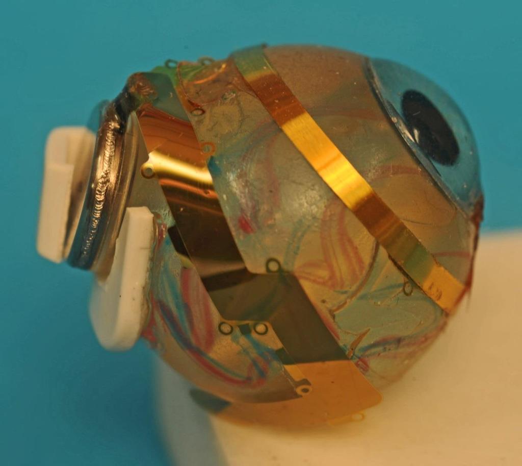
18 Package Assembly Pre-Molded Glued On Polyurethane Header Lip on Top Clamshell Assures Alignment Case Bottom Prepared for Projection Welding to Ferrule Upper and Lower Clamshell Halves Laser Welded Shut High Temperature Co-Fired Ceramic Disk with Signal Feedthroughs, Brazed to Titanium Ferrule April 4, 2014 The Boston Retinal Implant Project 18


19 Package Assembly II Co-fired ceramic feed-throughs have 256+ holes punched for individual stimulation sites Holes are filled with bio-compatible conductive material, fired, and brazed to the 11mm diameter Ti case Hermeticity measured by helium leak rate: 1x10E-09 to 1x10E-08 standard cc/sec April 4, 2014 The Boston Retinal Implant Project 19
20 Cofired Platinum /Alumina Feedthroughs The interaction of punched alumina substrates and Pt via metallizations upon firing were evaluated for the: Effect of particle size Effect of firing atmosphere Effect of alloying additives Effect of binder burn-out Effect of alumina / glass composition A robust materials and processing system was developed to allow air firing of feedthrough discs over a range of alumina compositions ( % alumina), that meet the hermeticity standard for medical implant devices 4/4/2014 The Boston Retinal Implant Project 20
 High Resolution Transmission electron microscopy (HREM) HREM Micrograph of Edge of Fired Via showing Void-free Alumina Pt Interface 4/4/2014 The Boston Retinal Implant")
21 Materials Analysis and Characterization Room temperature and high temperature X-ray diffraction Thermal analysis (DSC, TGA, dilatometry) Hermeticity testing (to 1 X 10 E(-9) std cc He/sec) Particle Analysis (BET, morphology) High Resolution Transmission electron microscopy (HREM) HREM Micrograph of Edge of Fired Via showing Void-free Alumina Pt Interface 4/4/2014 The Boston Retinal Implant Project 21


22 Internal Assembly of Device Solder paste is screened over the grid of the interior surface of the conductive feedthroughs The paste is melted to create solder bumps The bumps are mated with a matching pattern on the internal circuit board and the assembly is reflowed in an oven 4/4/2014 The Boston Retinal Implant Project 22


23 External Assembly of Device Electroplated Gold contacts are formed on the proximal end of the 256+ channel multi-electrode arrays The feedthroughs in the fired ceramic discs are similarly electro-plated with Gold The two parts are joined to one another using thermosonic bonding at 125 degrees C April 4, 2014 The Boston Retinal Implant Project 23

24 Discussion
1 P a g e INTRODUCTION
 1 P a g e INTRODUCTION A Bionic Eye is a device, which acts as an artificial eye. It is a broad term for the entire electronics system consisting of the image sensors, processors, radio transmitters &
VISUAL PROSTHESIS FOR MACULAR DEGENERATION AND RETINISTIS PIGMENTOSA
 VISUAL PROSTHESIS FOR MACULAR DEGENERATION AND RETINISTIS PIGMENTOSA 1 SHWETA GUPTA, 2 SHASHI KUMAR SINGH, 3 V K DWIVEDI Electronics and Communication Department 1 Dr. K.N. Modi University affiliated to
A Light Amplitude Modulated Neural Stimulator Design with Photodiode
 A Light Amplitude Modulated Neural Stimulator Design with Photodiode for Visual Prostheses Ji-Hoon Kim, Choul-Young Kim, and Hyoungho Ko* Department of Electronics, Chungnam National University, Daejeon,
The Boston retinal prosthesis a 15-channel hermetic wireless neural stimulator
 The Boston retinal prosthesis a 15-channel hermetic wireless neural stimulator The MIT Faculty has made this article openly available. Please share how this access benefits you. Your story matters. Citation
Probes and Electrodes Dr. Lynn Fuller Webpage:
 ROCHESTER INSTITUTE OF TECHNOLOGY MICROELECTRONIC ENGINEERING Probes and Electrodes Dr. Lynn Fuller Webpage: http://people.rit.edu/lffeee 82 Lomb Memorial Drive Rochester, NY 14623-5604 Tel (585) 475-2035
ACTIVE IMPLANTS. Glass Encapsulation
 ACTIVE IMPLANTS Glass Encapsulation OUTLINE Smart Implants Overview Cylindrical Glass Encapsulation CGE Planar Glass Encapsulation PGE Platform for Innovative Implantable Devices 5/7/2013 Glass Encapsulation
Simulation of Electrode-Tissue Interface with Biphasic Pulse Train for Epiretinal Prosthesis
 Simulation of Electrode-Tissue Interface with Biphasic Pulse Train for Epiretinal Prosthesis S. Biswas *1, S. Das 1,2, and M. Mahadevappa 2 1 Advaced Technology Development Center, Indian Institute of
B. Flip-Chip Technology
 B. Flip-Chip Technology B1. Level 1. Introduction to Flip-Chip techniques B1.1 Why flip-chip? In the development of packaging of electronics the aim is to lower cost, increase the packaging density, improve
A Comparison of Two and Three Dimensional Wire Antennas for Biomedical Applications. Shruthi Soora
 ABSTRACT SOORA, SHRUTHI. A Comparison of Two and Three Dimensional Wire Antennas for Biomedical Applications. (Under the direction of Prof. Gianluca Lazzi.) Miniature antennas are necessary to reduce the
Retinal stray light originating from intraocular lenses and its effect on visual performance van der Mooren, Marie Huibert
 University of Groningen Retinal stray light originating from intraocular lenses and its effect on visual performance van der Mooren, Marie Huibert IMPORTANT NOTE: You are advised to consult the publisher's
NIH Public Access Author Manuscript JAMA Ophthalmol. Author manuscript; available in PMC 2014 February 14.
 NIH Public Access Author Manuscript Published in final edited form as: JAMA Ophthalmol. 2013 February ; 131(2): 183 189. doi:10.1001/2013.jamaophthalmol.221. The Detection of Motion by Blind Subjects With
Digital Image Processing
 Digital Image Processing Lecture # 3 Digital Image Fundamentals ALI JAVED Lecturer SOFTWARE ENGINEERING DEPARTMENT U.E.T TAXILA Email:: ali.javed@uettaxila.edu.pk Office Room #:: 7 Presentation Outline
Innovation for success
 Innovation for success Success in the medical sector Thin film substrates for medical implants Retinal implants for Retina Implant AG, Germany Our mission: To restore sight to blind people and thus increase
Microelectronic Array for Stimulation of Retinal Tissue
 D. Scribner, L. Johnson, P. Skeath, R. Klein, F.K. Perkins, L. Wasserman, W. Bassett, D. Ilg, J. Peele, J. Friebele, J.G. Howard, W. Freeman, W. Krebs, and A. Taylor Microelectronic Array for Stimulation
HEREDITARY RETINAL DEGENERATIVE DISEASES,
 Visual Performance Using a Retinal Prosthesis in Three Subjects With Retinitis Pigmentosa DOUGLAS YANAI, JAMES D. WEILAND, MANJUNATHA MAHADEVAPPA, ROBERT J. GREENBERG, IONE FINE, AND MARK S. HUMAYUN PURPOSE:
The TRC-NW8F Plus: As a multi-function retinal camera, the TRC- NW8F Plus captures color, red free, fluorescein
 The TRC-NW8F Plus: By Dr. Beth Carlock, OD Medical Writer Color Retinal Imaging, Fundus Auto-Fluorescence with exclusive Spaide* Filters and Optional Fluorescein Angiography in One Single Instrument W
BIONIC EYE ( Offers new hope of restored vision ) BIONIC EYE ( Offers light at the end of tunnel for blind )
 BIONIC EYE ( Offers light at the end of tunnel for blind )") BIONIC EYE ( Offers new hope of restored vision ) EC0271 [1] SOWMYA.U.L [2] KALYANI.D.P ICE-2/4 ICE-2/4 GNITS-Hyderabad GNITS-Hyderabad BIONIC EYE ( Offers light at the end of tunnel for blind ) Introduction:
BIONIC EYE ( Offers new hope of restored vision ) EC0271 [1] SOWMYA.U.L [2] KALYANI.D.P ICE-2/4 ICE-2/4 GNITS-Hyderabad GNITS-Hyderabad BIONIC EYE ( Offers light at the end of tunnel for blind ) Introduction:
Visual prostheses: Current progress and challenges
 Visual prostheses: Current progress and challenges The MIT Faculty has made this article openly available. Please share how this access benefits you. Your story matters. Citation As Published Publisher
Sherlock Solder Models
 Introduction: Sherlock Solder Models Solder fatigue calculations in Sherlock are accomplished using one of the many solder models available. The different solder models address the type of package that
Package Architecture and Component Design for an Implanted Neural Stimulator with Closed Loop Control. Caroline K. Bjune
 Package Architecture and Component Design for an Implanted Neural Stimulator with Closed Loop Control Caroline K. Bjune There is this enormous mystery waiting to be unlocked, and the Brain Initiative will
Design of a high-resolution optoelectronic retinal prosthesis
 INSTITUTE OFPHYSICS PUBLISHING JOURNAL OFNEURALENGINEERING J. Neural Eng. 2 (2005) S105 S120 doi:10.1088/1741-2560/2/1/012 Design of a high-resolution optoelectronic retinal prosthesis Daniel Palanker
High Frequency Single & Multi-chip Modules based on LCP Substrates
 High Frequency Single & Multi-chip Modules based on Substrates Overview Labtech Microwave has produced modules for MMIC s (microwave monolithic integrated circuits) based on (liquid crystal polymer) substrates
The Department of Advanced Materials Engineering. Materials and Processes in Polymeric Microelectronics
 The Department of Advanced Materials Engineering Materials and Processes in Polymeric Microelectronics 1 Outline Materials and Processes in Polymeric Microelectronics Polymeric Microelectronics Process
NOTICE ASSOCIATE COUNSEL (PATENTS) CODE NAVAL RESEARCH LABORATORY WASHINGTON DC 20375
 CODE NAVAL RESEARCH LABORATORY WASHINGTON DC 20375") Serial No.: 09/635.226 Filing Date: 09 AUGUST 2000 Inventor: DEAN SCRIBNER NOTICE The above identified patent application is available for licensing. Requests for information should be addressed to: ASSOCIATE
Serial No.: 09/635.226 Filing Date: 09 AUGUST 2000 Inventor: DEAN SCRIBNER NOTICE The above identified patent application is available for licensing. Requests for information should be addressed to: ASSOCIATE
Recent Test Results of a Flight X-Band Solid-State Power Amplifier Utilizing GaAs MESFET, HFET, and PHEMT Technologies
 Recent Test Results of a Flight X-Band Solid-State Amplifier Utilizing GaAs MESFET, HFET, and PHEMT Technologies Elbert Nhan, Sheng Cheng, Marshall J. Jose, Steve O. Fortney, and John E. Penn The Johns
MICROSTRIP PATCH ANTENNA FOR A RETINAL PROSTHESIS
 MICROSTRIP PATCH ANTENNA FOR A RETINAL PROSTHESIS DR.S.RAGHAVAN*, G.ANANTHA KUMAR *Dr.S.Raghavan is a Senior Faculty of the Department of Electronics and Communication Engg., National Institute of Technology,
23. Packaging of Electronic Equipments (2)
") 23. Packaging of Electronic Equipments (2) 23.1 Packaging and Interconnection Techniques Introduction Electronic packaging, which for many years was only an afterthought in the design and manufacture of
23. Packaging of Electronic Equipments (2) 23.1 Packaging and Interconnection Techniques Introduction Electronic packaging, which for many years was only an afterthought in the design and manufacture of
EYE ANATOMY. Multimedia Health Education. Disclaimer
 Disclaimer This movie is an educational resource only and should not be used to manage your health. The information in this presentation has been intended to help consumers understand the structure and
BGA (Ball Grid Array)
") BGA (Ball Grid Array) National Semiconductor Application Note 1126 November 2002 Table of Contents Introduction... 2 Package Overview... 3 PBGA (PLASTIC BGA) CONSTRUCTION... 3 TE-PBGA (THERMALLY ENHANCED
BGA (Ball Grid Array) National Semiconductor Application Note 1126 November 2002 Table of Contents Introduction... 2 Package Overview... 3 PBGA (PLASTIC BGA) CONSTRUCTION... 3 TE-PBGA (THERMALLY ENHANCED
Development of an Indirect Resistance Brazing Technology for Sandwich Metal Panels
 Development of an Indirect Resistance Brazing Technology for Sandwich Metal Panels Jerry Gould, EWI, Columbus, OH Doug Cox, CellTechMetals, San Diego, CA CellTech Metals is developing a new generation
Design of Experiments Technique for Microwave / Millimeter Wave. Flip Chip Optimization
 Design of Experiments Technique for Microwave / Millimeter Wave Flip Chip Optimization Daniela Staiculescu*, Joy Laskar, Manos Tentzeris School of Electrical and Computer Engineering Packaging Research
2 The First Steps in Vision
 2 The First Steps in Vision 2 The First Steps in Vision A Little Light Physics Eyes That See light Retinal Information Processing Whistling in the Dark: Dark and Light Adaptation The Man Who Could Not
User s Guide to. Centre for Materials for Electronics Technology Panchawati, Off Pashan Road, Pune September Version 2.
 User s Guide to Centre for Materials for Electronics Technology Panchawati, Off Pashan Road, Pune 411008 September 2013 Version 2.1 Contents 1 Designing of LTCC Structures and Design Rules... 01 1.1 Guidelines
PSY 214 Lecture # (09/14/2011) (Introduction to Vision) Dr. Achtman PSY 214. Lecture 4 Topic: Introduction to Vision Chapter 3, pages 44-54
 (Introduction to Vision) Dr. Achtman PSY 214. Lecture 4 Topic: Introduction to Vision Chapter 3, pages 44-54") Corrections: A correction needs to be made to NTCO3 on page 3 under excitatory transmitters. It is possible to excite a neuron without sending information to another neuron. For example, in figure 2.12
Corrections: A correction needs to be made to NTCO3 on page 3 under excitatory transmitters. It is possible to excite a neuron without sending information to another neuron. For example, in figure 2.12
CHAPTER 11: Testing, Assembly, and Packaging
 Chapter 11 1 CHAPTER 11: Testing, Assembly, and Packaging The previous chapters focus on the fabrication of devices in silicon or the frontend technology. Hundreds of chips can be built on a single wafer,
System Implementation of a CMOS vision chip for visual recovery
 System Implementation of a CMOS vision chip for visual recovery Akihiro Uehara a, David C. Ng, Tetsuo Furumiya, Keiichi Isakari, Keiichiro Kagawa, Takashi Tokuda, Jun Ohta, Masahiro Nunoshita Nara Institute
Research on Image Processing System for Retinal Prosthesis
 International Symposium on Computers & Informatics (ISCI 2015) Research on Image Processing System for Retinal Prosthesis Wei Mao 1,a, Dashun Que 2,b, Huawei Chen 1, Mian Yao 1 1 School of Information
MICROELECTRONICS ASSSEMBLY TECHNOLOGIES. The QFN Platform as a Chip Packaging Foundation
 West Coast Luncheon January 15, 2014. PROMEX PROMEX INDUSTRIES INC. MICROELECTRONICS ASSSEMBLY TECHNOLOGIES The QFN Platform as a Chip Packaging Foundation 3075 Oakmead Village Drive Santa Clara CA Ɩ 95051
Vision. By: Karen, Jaqui, and Jen
 Vision By: Karen, Jaqui, and Jen Activity: Directions: Stare at the black dot in the center of the picture don't look at anything else but the black dot. When we switch the picture you can look around
Applications of Optics
 Nicholas J. Giordano www.cengage.com/physics/giordano Chapter 26 Applications of Optics Marilyn Akins, PhD Broome Community College Applications of Optics Many devices are based on the principles of optics
Retinitis pigmentosa (RP) and age-related macular degeneration
 and age-related macular degeneration") Translational Frequency and Amplitude Modulation Have Different Effects on the Percepts Elicited by Retinal Stimulation Devyani Nanduri, 1,2 Ione Fine, 3 Alan Horsager, 4,5 Geoffrey M. Boynton, 3 Mark
Translational Frequency and Amplitude Modulation Have Different Effects on the Percepts Elicited by Retinal Stimulation Devyani Nanduri, 1,2 Ione Fine, 3 Alan Horsager, 4,5 Geoffrey M. Boynton, 3 Mark
Research in Support of the Die / Package Interface
 Research in Support of the Die / Package Interface Introduction As the microelectronics industry continues to scale down CMOS in accordance with Moore s Law and the ITRS roadmap, the minimum feature size
EC-433 Digital Image Processing
 EC-433 Digital Image Processing Lecture 2 Digital Image Fundamentals Dr. Arslan Shaukat 1 Fundamental Steps in DIP Image Acquisition An image is captured by a sensor (such as a monochrome or color TV camera)
An Arbitrary Waveform 16 Channel Neural Stimulator with Adaptive Supply Regulator in 0.35 µm HV CMOS for Visual Prosthesis
 JOURNAL OF SEMICONDUCTOR TECHNOLOGY AND SCIENCE, VOL.13, NO.1, FEBRUARY, 213 http://dx.doi.org/1.5573/jsts.213.13.1.79 An Arbitrary Waveform 16 Channel Neural Stimulator with Adaptive Supply Regulator
Outline of the Talk. Retinal Prosthesis Goal. Retinitis Pigmentosa. Human Visual System ISSCC 2004 / SESSION 12 / BIOMICROSYSTEMS / 12.
 ISSCC 004 / SESSION / BIOMICROSYSTEMS /.. Retinal Prosthesis Wentai iu, Mark S. Humayun University of California, Santa Cruz, CA University of Southern California, os Angeles, CA A prosthesis device is
MA4P7470F-1072T. Non Magnetic MELF PIN Diode. Features. Description and Applications. Designed for Automated Assembly
 Features Non-Magnetic Package Suitable for MRI Applications Rectangular MELF SMQ Ceramic Package Hermetically Sealed Low Rs for Low Insertion Loss Long τ L for Low Intermodulation Distortion Low Cj for
Advanced Packaging - Pulsed-laser Heating for Flip Chip Assembly
 Page 1 of 5 Pulsed-laser Heating for Flip Chip Assembly A stress-free alternative By Thorsten Teutsch, Ph.D., Pac Tech USA, Elke Zakel, Ph.D., and Ghassem Azdasht, Pac Tech GmbH As flip chip applications
How to Build an LED Projector
 How to Build an LED Projector SLEDS Project Organization Overview Design/Grow SLEDS (UIowa & Teledyne) Test/Optimize discrete SLEDS devices (U Iowa) Develop CMOS Drivers & Process, Package, Test Arrays
Market and technology trends in advanced packaging
 Close Market and technology trends in advanced packaging Executive OVERVIEW Recent advances in device miniaturization trends have placed stringent requirements for all aspects of product manufacturing.
BMC s heritage deformable mirror technology that uses hysteresis free electrostatic
 Optical Modulator Technical Whitepaper MEMS Optical Modulator Technology Overview The BMC MEMS Optical Modulator, shown in Figure 1, was designed for use in free space optical communication systems. The
The Special Senses: Vision
 OLLI Lecture 5 The Special Senses: Vision Vision The eyes are the sensory organs for vision. They collect light waves through their photoreceptors (located in the retina) and transmit them as nerve impulses
Chip Assembly on MID (Molded Interconnect Device) A Path to Chip Modules with increased Functionality
 A Path to Chip Modules with increased Functionality") T e c h n o l o g y Dr. Werner Hunziker Chip Assembly on MID (Molded Interconnect Device) A Path to Chip Modules with increased Functionality The MID (Molded Interconnect Device) technology enables the
T e c h n o l o g y Dr. Werner Hunziker Chip Assembly on MID (Molded Interconnect Device) A Path to Chip Modules with increased Functionality The MID (Molded Interconnect Device) technology enables the
GFM DC-DC Converter. Preliminary 8 to 50 Volt Input 30 Watt High Efficiency. MIL-STD Pedigree. Exceptional Value. PRELIMINARY
 Features High reliability Typical efficiency 90% or greater Up to 30 watts -55 C to +105 C operation Wide 8 to 50 volt input Inhibit and sync functions Assembled in a MIL-PRF-38534 certified facility GFM
Optics B. Science Olympiad North Regional Tournament at the University of Florida DO NOT WRITE ON THIS BOOKLET. THIS IS AN TEST SET.
 Optics B Science Olympiad North Regional Tournament at the University of Florida 1 DO NOT WRITE ON THIS BOOKLET. THIS IS AN TEST SET. Part I: General Body Knowledge Questions 2 1) (3 PTS) For much of the
64 Channel Flip-Chip Mounted Selectively Oxidized GaAs VCSEL Array
 64 Channel Flip-Chip Mounted Selectively Oxidized GaAs VCSEL Array 69 64 Channel Flip-Chip Mounted Selectively Oxidized GaAs VCSEL Array Roland Jäger and Christian Jung We have designed and fabricated
US A United States Patent [19] [11] Patent Number: 6,156,978 [57] ABSTRACT 174/152 GM 174/152 GM 174/152 GM 174/152 GM 250/ /44
![US A United States Patent [19] [11] Patent Number: 6,156,978 [57] ABSTRACT 174/152 GM 174/152 GM 174/152 GM 174/152 GM 250/ /44](/thumbs/96/128483934.jpg "US A United States Patent [19] [11] Patent Number: 6,156,978 [57] ABSTRACT 174/152 GM 174/152 GM 174/152 GM 174/152 GM 250/ /44") 111111111111111111111111111111111111111111111111111111111111111111111111111 US006156978A United States Patent [19] [11] Patent Number: Peck et al. [45] Date of Patent: Dec. 5, 2000 [54] ELECTRICAL FEEDTHROUGH
111111111111111111111111111111111111111111111111111111111111111111111111111 US006156978A United States Patent [19] [11] Patent Number: Peck et al. [45] Date of Patent: Dec. 5, 2000 [54] ELECTRICAL FEEDTHROUGH
Application Bulletin 240
 Application Bulletin 240 Design Consideration CUSTOM CAPABILITIES Standard PC board fabrication flexibility allows for various component orientations, mounting features, and interconnect schemes. The starting
Chapter 11 Testing, Assembly, and Packaging
 Chapter 11 Testing, Assembly, and Packaging Professor Paul K. Chu Testing The finished wafer is put on a holder and aligned for testing under a microscope Each chip on the wafer is inspected by a multiple-point
Photovoltaic Restoration of Sight with High Visual Acuity in Rats with Retinal Degeneration
 Photovoltaic Restoration of Sight with High Visual Acuity in Rats with Retinal Degeneration D. Palanker 1,2, G. Goetz 1, H. Lorach 1, Y. Mandel 1, R. Smith 4, D. Boinagrov 1, X. Lei 3, T. Kamins 3, J.
Manufacturing Processes (continued)
") Manufacturing (continued) Machining Some other processes Material compatibilities Process (shape) capabilities Manufacturing costs Correct pg 142, question 34i should read Fig 6.18 question 34j should
Manufacturing (continued) Machining Some other processes Material compatibilities Process (shape) capabilities Manufacturing costs Correct pg 142, question 34i should read Fig 6.18 question 34j should
Video Microscopy of Selective Laser Sintering. Abstract
 Video Microscopy of Selective Laser Sintering Lawrence S. Melvin III, Suman Das, and Joseph J. Beaman Jr. Department of Mechanical Engineering The University of Texas at Austin Abstract This paper presents
True Three-Dimensional Interconnections
 True Three-Dimensional Interconnections Satoshi Yamamoto, 1 Hiroyuki Wakioka, 1 Osamu Nukaga, 1 Takanao Suzuki, 2 and Tatsuo Suemasu 1 As one of the next-generation through-hole interconnection (THI) technologies,
Image sensor combining the best of different worlds
 Image sensors and vision systems Image sensor combining the best of different worlds First multispectral time-delay-and-integration (TDI) image sensor based on CCD-in-CMOS technology. Introduction Jonathan
16 to 50 volts input 25 Watt
 Features 16 to 50 volt input Up to 87% efficiency, 42 W/in 3 Available to Class H, MIL-PRF-38534 Undervoltage lockout -55 C to +125 C operation Fully isolated, magnetic feedback Fixed frequency, 500 khz
Light has some interesting properties, many of which are used in medicine:
 LIGHT IN MEDICINE Light has some interesting properties, many of which are used in medicine: 1- The speed of light changes when it goes from one material into another. The ratio of the speed of light in
Extending Acoustic Microscopy for Comprehensive Failure Analysis Applications
 Extending Acoustic Microscopy for Comprehensive Failure Analysis Applications Sebastian Brand, Matthias Petzold Fraunhofer Institute for Mechanics of Materials Halle, Germany Peter Czurratis, Peter Hoffrogge
SMP-CGA DIRECT MOUNT, SOLDERLESS SOCKET FOR BURN-IN AND TEST APPLICATIONS
 38.500 SMP-CGA DIRECT MOUNT, SOLDERLESS SOCKET FOR BURN-IN AND TEST APPLICATIONS FEATURES: Wide temperature range (-55C to +155C ) xga IC High current capability (up to 4A ) Excellent signal integrity
10/3/2012. Study Harder
 This presentation is a professional collaboration of development time prepared by: Rex Christensen Terri Jurkiewicz and Diane Kawamura Study Harder CR detection is inefficient, inferior to film screen
Visual Perception. human perception display devices. CS Visual Perception
 Visual Perception human perception display devices 1 Reference Chapters 4, 5 Designing with the Mind in Mind by Jeff Johnson 2 Visual Perception Most user interfaces are visual in nature. So, it is important
While digital techniques have the potential to reduce patient doses, they also have the potential to significantly increase them.
 In press 2004 1 2 Guest Editorial (F. Mettler, H. Ringertz and E. Vano) Guest Editorial (F. Mettler, H. Ringertz and E. Vano) Digital radiology An appropriate analogy that is easy for most people to understand
Electronic materials and components-semiconductor packages
 Electronic materials and components-semiconductor packages Semiconductor back-end processes We will learn much more about semiconductor back end processes in subsequent modules, but you need to understand
Vision. The eye. Image formation. Eye defects & corrective lenses. Visual acuity. Colour vision. Lecture 3.5
 Lecture 3.5 Vision The eye Image formation Eye defects & corrective lenses Visual acuity Colour vision Vision http://www.wired.com/wiredscience/2009/04/schizoillusion/ Perception of light--- eye-brain
Two major features of this text
 Two major features of this text Since explanatory materials are systematically made based on subject examination questions, preparation
KH200 Fast Settling, Wideband Operational Amplifier
 Fast Settling, Wideband Operational Amplifier www.cadeka.com Features -3dB bandwidth of 95MHz 0.1% settling in 18ns 4000V/µs slew rate Low distortion, linear phase 3.6ns rise and fall times Direct replacement
Fitting Optical Interconnects to an Electrical World- Packaging and Reliability Issues of Arrayed Optoelectronic Modules Keith Goossen, University of
 Fitting Optical Interconnects to an Electrical World- Packaging and Reliability Issues of Arrayed Optoelectronic Modules Keith Goossen, University of Delaware 1 OUTLINE 1. Technology a. Physical rack limitations
DATASHEET ISL9021A. Features. Pinouts. Applications. 250mA Single LDO with Low I Q, Low Noise and High PSRR LDO. FN6867 Rev 2.
 NOT RECOMMENDED FOR NEW DESIGNS RECOMMENDED REPLACEMENT PART ISL9021A 250mA Single LDO with Low I Q, Low Noise and High PSRR LDO DATASHEET FN6867 Rev 2.00 The ISL9021 is a single LDO providing high performance
Fiber-Optic Transceivers for High-speed Digital Interconnects in Satellites
 Photo: ESA Fiber-Optic Transceivers for High-speed Digital Interconnects in Satellites ICSO conference, 9 Oct 2014 Mikko Karppinen (mikko.karppinen@vtt.fi), V. Heikkinen, K. Kautio, J. Ollila, A. Tanskanen
SOLDER BUMP FLIP CHIP BONDING FOR PIXEL DETECTOR HYBRIDIZATION
 SOLDER BUMP FLIP CHIP BONDING FOR PIXEL DETECTOR HYBRIDIZATION Jorma Salmi and Jaakko Salonen VTT Information Technology Microelectronics P.O. Box 1208 FIN-02044 VTT, Finland (visiting: Micronova, Tietotie
A Readout ASIC for CZT Detectors
 A Readout ASIC for CZT Detectors L.L.Jones a, P.Seller a, I.Lazarus b, P.Coleman-Smith b a STFC Rutherford Appleton Laboratory, Didcot, OX11 0QX, UK b STFC Daresbury Laboratory, Warrington WA4 4AD, UK
STUDY NOTES UNIT I IMAGE PERCEPTION AND SAMPLING. Elements of Digital Image Processing Systems. Elements of Visual Perception structure of human eye
 DIGITAL IMAGE PROCESSING STUDY NOTES UNIT I IMAGE PERCEPTION AND SAMPLING Elements of Digital Image Processing Systems Elements of Visual Perception structure of human eye light, luminance, brightness
PCB Antenna with Cable Integration Application Note Version 4
 PCB Antenna with Cable Integration Application Note Version 4 CONTENTS 1. BASICS 2. APPLICATIONS 3. SIZE 4. SHAPE 5. GROUND PLANE SIZE 6. IMPEDANCE 7. BANDWIDTH 8. VSWR 9. GAIN 10. EFFICIENCY 11. POLARIZATION
Brief Introduction of Sigurd IC package Assembly
 Brief Introduction of Sigurd IC package Assembly Content Package Development Trend Product Brief Sawing type QFN Representative MEMS Product LGA Light Sensor Proximity Sensor High Yield Capability Low
Optoelectronics Packaging Research at UIC. Peter Borgesen, Ph.D. Project Manager
 Optoelectronics Packaging Research at UIC Peter Borgesen, Ph.D. Project Manager Abstract The present document offers a brief overview of ongoing research into photonic packaging issues within the SMT Laboratory
14 to 50 volt input - 35 watt
 Features Input voltage range 14 to 50 volts Transient protection up to 80 volts for one second Indefinite short circuit protection -55 C to +125 C operation Magnetic feedback Synchronization Inhibit function
Choices and Vision. Jeffrey Koziol M.D. Thursday, December 6, 12
 Choices and Vision Jeffrey Koziol M.D. How does the eye work? What is myopia? What is hyperopia? What is astigmatism? What is presbyopia? How the eye works How the Eye Works 3 How the eye works Light rays
Lone Star Neuromodulation
 Lone Star Neuromodulation Disruptive Pulse-Generator Technology Platform 1 Our Vision Target unmet clinical needs by creating a disruptive device platform that offers promising solutions for lowering costs,
Evaluation of Package Properties for RF BJTs
 Application Note Evaluation of Package Properties for RF BJTs Overview EDA simulation software streamlines the development of digital and analog circuits from definition of concept and estimation of required
Monolithic Amplifier CMA-103+ Ultra Linear Low Noise, Ceramic to 4 GHz
 Ultra Linear Low Noise, Ceramic Monolithic Amplifier 50Ω 0.05 to 4 GHz The Big Deal Ceramic, hermetically sealed, nitrogen filled Low profile case, 0.045 Ultra High IP3 Broadband High Dynamic Range CASE
Lecture 2 Digital Image Fundamentals. Lin ZHANG, PhD School of Software Engineering Tongji University Fall 2016
 Lecture 2 Digital Image Fundamentals Lin ZHANG, PhD School of Software Engineering Tongji University Fall 2016 Contents Elements of visual perception Light and the electromagnetic spectrum Image sensing
Silicon PIN Limiter Diodes V 5.0
 5 Features Lower Insertion Loss and Noise Figure Higher Peak and Average Operating Power Various P1dB Compression Powers Lower Flat Leakage Power Reliable Silicon Nitride Passivation Description M/A-COM
Section 2 concludes that a glare meter based on a digital camera is probably too expensive to develop and produce, and may not be simple in use.
 Possible development of a simple glare meter Kai Sørensen, 17 September 2012 Introduction, summary and conclusion Disability glare is sometimes a problem in road traffic situations such as: - at road works
CHAPTER 4 LOCATING THE CENTER OF THE OPTIC DISC AND MACULA
 90 CHAPTER 4 LOCATING THE CENTER OF THE OPTIC DISC AND MACULA The objective in this chapter is to locate the centre and boundary of OD and macula in retinal images. In Diabetic Retinopathy, location of
Application Note 5026
 Surface Laminar Circuit (SLC) Ball Grid Array (BGA) Eutectic Surface Mount Assembly Application Note 5026 Introduction This document outlines the design and assembly guidelines for surface laminar circuitry
Capabilities of Flip Chip Defects Inspection Method by Using Laser Techniques
 Capabilities of Flip Chip Defects Inspection Method by Using Laser Techniques Sheng Liu and I. Charles Ume* School of Mechanical Engineering Georgia Institute of Technology Atlanta, Georgia 3332 (44) 894-7411(P)
RETINAL PROSTHESES. Daniel Palanker and Georges Goetz
 Restoring sight with RETINAL PROSTHESES Daniel Palanker and Georges Goetz By implanting electrodes that transmit visual information to the surviving neurons in a diseased retina, it s possible to bring
GA A26816 DESIGNS OF NEW COMPONENTS FOR ITER ECH&CD TRANSMISSION LINES
 GA A26816 DESIGNS OF NEW COMPONENTS FOR ITER ECH&CD TRANSMISSION LINES by R.A. OLSTAD, J.L. DOANE, C.P. MOELLER and C.J. MURPHY JULY 2010 DISCLAIMER This report was prepared as an account of work sponsored
Advances in X-Ray Technology for Semicon Applications Keith Bryant and Thorsten Rother
 Advances in X-Ray Technology for Semicon Applications Keith Bryant and Thorsten Rother X-Ray Champions, Telspec, Yxlon International Agenda The x-ray tube, the heart of the system Advances in digital detectors
Bob Willis Process Guides
 What is a Printed Circuit Board Pad? What is a printed circuit board pad, it may sound like a dumb question but do you stop to think what it really does and how its size is defined and why? A printed circuit
ROBOT VISION. Dr.M.Madhavi, MED, MVSREC
 ROBOT VISION Dr.M.Madhavi, MED, MVSREC Robotic vision may be defined as the process of acquiring and extracting information from images of 3-D world. Robotic vision is primarily targeted at manipulation
Process Certification and Defect Recognition: Hybrids, Microcircuits and RF/MMIC Modules (3 DAYS)
") Process Certification and Defect Recognition: Hybrids, Microcircuits and RF/MMIC Modules (3 DAYS) Course Description: Most companies struggle to introduce new lines and waste countless manhours and resources
Process Certification and Defect Recognition: Hybrids, Microcircuits and RF/MMIC Modules (3 DAYS) Course Description: Most companies struggle to introduce new lines and waste countless manhours and resources