INTRODUCTION TO SILICON PHOTONICS CIRCUIT DESIGN
|
|
|
- Alan Bruce Lawson
- 5 years ago
- Views:
Transcription

1 INTRODUCTION TO SILICON PHOTONICS CIRCUIT DESIGN Wim Bogaerts Short Course OFC


2 WHAT IS SILICON PHOTONICS? OFC 2018 Short Course SC454 The implementation of high density photonic integrated circuits by means of CMOS process technology in a CMOS fab Enabling complex optical functionality on a compact chip at low cost 8
 OFC 2018 Short Course SC454")

3 PHOTONIC INTEGRATED CIRCUITS (PIC) OFC 2018 Short Course SC454 Integration of (many) optical functions on a chip Source: EECS Berkeley 9


 fiber-to-the-home bidirectional")
 monolithic receiver (eg 16x20Gb/s)")
4 INDUSTRIAL TAKE-UP EXAMPLES IN TELECOM/DATACOM/DATA CENTERS active optical cables (eg PSM4: 4x28 Gb/s on parallel fibers) WDM transceivers (eg 4 WDM channels x 25 Gb/s on single fiber) coherent receiver (eg 100 Gb/s PM-QPSK) fiber-to-the-home bidirectional transceiver (eg 12 x 2.5 Gb/s) monolithic receiver (eg 16x20Gb/s) 40Gb/s, 50Gb/s and 100 Gb/s Ethernet (future: 400Gb/s) 10
5 WHY SILICON PHOTONICS? OFC 2018 Short Course SC454 Large scale manufacturing Scale Submicron-scale waveguides 11
6 SCALING OPTICAL WAVEGUIDES: INDEX CONTRAST III-V semiconductors index contrast ~ 10% 1mm Glass waveguide index contrast ~0.1% 1mm SOI wire silicon wire: index contrast ~ 200% 12


7 WAVEGUIDES: SILICON PHOTONIC WIRES High contrast waveguides submicrometer dimensions small bend radius Si 200 nm SiO nm silicon-oxide Si substrate optical mode 13


8 HIGH INDEX CONTRAST: A BLESSING AND A CURSE Very tight confinement of light Si SiO 2 Very small bend radii : down to 1 mm [2um box] Very dense integration of components on a chip Sub-wavelength freedom Photonic crystals with extremely high quality cavities Cheben, OE,


9 50 mm 4 mm OFC 2018 Short Course SC mm HIGHER CONTRAST, SMALLER CORES, TIGHTER BENDS Silica on silicon Indium Phosphide Contrast ~ Mode diameter ~ 8µm Bend radius ~ 5mm Contrast ~ Size ~ 10 cm Silicon on insulator 2 Mode diameter ~ 2µm Bend radius ~ 0.5mm Contrast ~ Size ~ 10mm 2 Mode diameter ~ 0.4µm Bend radius ~ 5µm Size ~ 0.1mm 2 15
10 HIGH INDEX CONTRAST: A BLESSING AND A CURSE Every nm 3 matters CMOS technology is the only manufacturing technology with sufficient nm-process control to take advantage of the blessing without suffering from the curse Si SiO 2 [2um box] 16


11 WAVEGUIDES Waveguide losses dominated by scattering. Use better litho + etch 1µm sidewall roughness 17


12 COMPACT BENDS, TRANSITIONS, CROSSINGS rib waveguide 2µm 3 µm Waveguide Crossing: 97% transmission wire waveguide 18

13 FIBER-TO-CHIP COUPLING Vertical fiber interface: allows easy on-chip testing 10 TE 19
14 Transmission Transmission Transmission Normalized transmission OFC 2018 Short Course SC454 WAVELENGTH FILTERING FUNCTIONS Light is a wave: interference at the 100nm scale interferometers resonators e.g. ring resonator λ fit: Q = 15600± λ λ 0.1 fit: Q = 15400± Wavelength [nm] 20
15 WAVELENGTH FILTERING FUNCTIONS Arrayed waveguide grating dispersive delay lines: each wavelength feels a different phase delay output star coupler: different phase delays create a phase front focussing into different output waveguides input star coupler: light is distributed over many delay lines
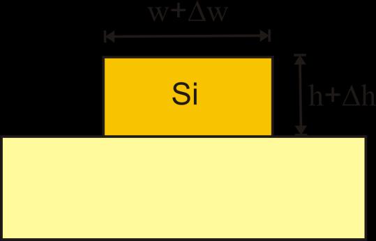
16 SENSITIVITY OF SILICON PHOTONICS WAVELENGTH FILTERS Silicon photonic waveguides are sensitive to geometry stress temperature wire width wire height temperature λ w 1 λ h 2 λ T 0.08 nm Τ nm nm Τ nm 1nm ~20K 1nm ~10K nm K wavelength w h Si SiO 2 22


17 Optical Power (mw) OFC 2018 Short Course SC454 INTEGRATED HEATERS FOR CONTROL Different types of electrical resistors: metal, silicide, doped silicon Copper traces Tungsten pillars Optional undercut to lower reduce thermal leakage Measured Optical Power Optical Power Fit 1.5mW/π oxide silicon resistor oxide oxide silicon waveguide undercut region Electric Power (mw) 23
18 ELECTRO-OPTIC EFFECT IN SILICON: INJECTION VS. DEPLETION Carrier injection p-i-n diode in forward bias Inject carriers into waveguides Strong effect (many carriers) Slow effect (~1GHz) Carrier depletion p-n diode in reverse bias Extract carriers from waveguide Weaker effect Fast effect (>40GHz) Carrier accumulation p p p p n n n n Accumulation at oxide Similar to capacitor Fast p n 24


19 ELECTRICAL SIGNAL MODULATION Add doped junction to silicon waveguide: modulate refractive index travelling wave modulator 1mm 20µm ring resonator modulator metal p n metal waveguide 25


20 GERMANIUM ELECTRO-ABSORPTION MODULATOR Advantages Uses existing Ge-detector technology Compact, optical BW > 35nm 3dB BW > 40GHz Next steps Ge SiGe to reach C-band Ge-laser Gupta, S., et al. 50GHz Ge Waveguide Electro-Absorption Modulator Integrated in a 220nm SOI Photonics Platform. In Optical Fiber Communication Conference (Vol. 1, pp. 5 7)


21 FAST AND EFFICIENT PHOTODETECTORS Integrated Germanium Photodetectors 1 A/W responsivity > 70 GHz bandwidth 3nA dark current 1 V operation 27


22 INTEGRATION ON WAFER SCALE light transport wavelength filtering signal modulation detection Compatible with CMOS processing 28


23 ALL PHOTONIC FUNCTIONS ARE THERE OFC 2018 Short Course SC454 light source except for the laser. 30


24 LASER INTEGRATION ON SILICON PHOTONICS Transfer III-V laser material to the silicon Photonic chip III-V wafer DVS-BCB SiO 2 Silicon waveguide SiO 2 Buried oxide 31


25 LASER INTEGRATION ON SILICON PHOTONICS Different laser types DFB, DBR, microdisk, external cavity, multiwavelength, modelocked, 32

26 SILICON PHOTONICS ENABLES LARGE SCALE PHOTONICS >10000 optical functions on a chip optical guiding, filtering, detection and modulation efficient fiber-chip coupling external or integrated light sources 33


27 MORE THAN JUST PHOTONS Silicon photonics goes beyond the optical chip software configuration 1000s electronic feedback loops 1000s electrical IOs 100s optical IOs 10s RF signals 10000s optical elements 34


28 THE PHOTONIC CHIP IS JUST A PART OF THE SYSTEM integrated package photonics analog electronics digital electronics software user 35


29 PACKAGING TECHNOLOGY OFC 2018 Short Course SC454 fiber arrays Combining photonics and electronics Fiber interfaces RF connections Thermal and mechanical multi-core fibers shielded packages 36


30 FABLESS SILICON PHOTONICS Many fabless Silicon Photonics companies have emerged from direct collaboration with fabs (Luxtera,...) starting from MPW (Caliopa, Genalyte, Acacia) Established players are also partnering e.g. Finisar with ST Many keep their fab a secret How to enter as a new (fabless) startup? 37
")
31 SMALL BUILDING BLOCKS LARGE CIRCUITS μm-scale building blocks cm-scale chips thousands millions components Photonics Very Large Scale Integration (VLSI) 38


 technological potential of 10000+")
32 COMPLEXITY AS AN ENABLER Integrated Electronics billions of digital gates: unprecedented logic performance millions of analog transistors: unprecedented control (even with imperfect components: enabled by!) More elements More complexity More functionality Integrated Photonics (Silicon Photonics) technological potential of photonic elements on a chip not even scratched the surface of what this could do 39
33 PHOTONIC CIRCUIT DESIGN 40

 Variability analysis on circuits Yield prediction")
34 ENABLING COMPLEXITY IN PHOTONICS Industrial PIC technology platforms (Si, InP, ) demonstrations of sensors, spectrometers, commercial products But: fairly simple circuits ~ 1970s ICs More complexity is enabled by methods Design capture: translating ideas to circuits Circuit simulation (electrical+photonic) Variability analysis on circuits Yield prediction and improvement 41

35 COMPLEX CIRCUITS COMPLICATED BUILDING BLOCKS You can do a lot with a few building blocks Electronics: Transistors, Resistors, Diodes, Photonics: Waveguides, Directional couplers, Complexity emerges from connectivity But you need to support complexity - Accurate models - Variability - Parasitics 42


 tools!")
36 DESIGNING PHOTONIC INTEGRATED CIRCUITS Can we learn from electronic ICs? Millions of analog transistors Billions of digital transistors Power, timing and yield First time right s Very mature Electronic Design Automation (EDA) tools! A well established flow Can we repurpose this for photonics? 43


37 DESIGN ENVIRONMENTS ARE EMERGING Combinations of Photonics Design and EDA Physical simulation combined with circuit Physical and functional verification First PDKs with basic models 44
38 WHAT IS A DESIGN FLOW? OFC 2018 Short Course SC454 Design is the creation of a plan or convention for the construction of an object or a system Design Flow a repeatable pattern of activity, usually involving multiple tasks with a specific set of outcomes 45


39 WHAT IS THE PURPOSE OF A DESIGN FLOW? OFC 2018 Short Course SC454 idea/ concept a working chip to translate an idea into a WORKING chip. 46
40 A TYPICAL DESIGN CYCLE idea/ concept function simulate function layout check rules verify function fabricate device test Front-End Back-End flow time 49
41 A GREAT IDEA? OFC 2018 Short Course SC454 idea/ concept function Questions to be asked simulate function layout check rules verify function What should my device do? fabricate device What are its operational principles? How well should it perform? Where/How will it be used? test To go from an idea to a, you need SPECIFICATIONS flow time 52
42 DESIGN CAPTURE AND SIMULATION idea/ concept function simulate function layout check rules Capture intent in verify a functional fabricate description test device function underlying equations behavioral models flow of information This typically results in a schematic circuit flow time 53

 and which")


43 DESIGN CAPTURE Select/construct functional blocks Connect them together Netlist: list of connections ( Nets ) and which components the nets are attached to. Schematic: graphical representation of arm1 a netlist, with placements dc dc Example: Mach Zehnder Interferometer arm2 54


 interface to")
44 SCHEMATIC EDITOR drag and dropping components and drawing connections make waveguides explicit if needed component libraries parametrization scriptability different connections (waveguides, direct optical, electrical) interface to circuit simulation specify I/O ports 55

45 HIERARCHY Netlists are hierarchical dc wg OFC 2018 Short Course SC454 Hierarchical cells: contain another netlist Atomic cells: contain a circuit model wg arm1 ring1 wg dc dc Example: Ring-Loaded Mach Zehnder Interferometer arm2 56
46 WAVEGUIDES IN PHOTONIC SCHEMATICS What are waveguides? Simple connections between building blocks the length and shape does not really matter it should just provide a good connection similar as an electrical wire Functional building blocks with a certain phase/time delay length and shape are very important should be treated as a building block The distinction is important phase sensitive (delay in MZI) separate building block arm2 direct (logical) connection just a waveguide link to the output grating coupler splitter combiner grating coupler arm1 57


47 DESIGN CAPTURE AND SIMULATION idea/ concept function simulate function layout check rules Capture intent in verify a functional fabricate description test device function underlying equations behavioral models flow of information This typically results in a schematic circuit Simulated at an abstract level Optimization: an iterative process flow time 58

48 COMPONENT SIMULATION CIRCUIT SIMULATION Physical models Circuit simulations Accurate, slow Based on actual geometries Best model = reality Approximate, fast Based on functional description behavioural models 59


49 MODELS Should allow simulation in a larger circuit - based on equations - based on measurement data - based on EM simulations Photonics: Nothing really standardized No standardized simulation method No standard model description No standard signals 60

")

50 OPTICAL VS. ELECTRICAL CIRCUIT SIMULATION optics = electric at very high frequency ultra-small time steps (fs) ultra-long simulations (10 12 time steps) high-bandwidth signals (200THz) zoom period ~5fs impractical. Solution: analytic signal = complex amplitude on carrier complex envelope amplitude phase of carrier 61

51 PHOTONIC CIRCUIT SIMULATIONS Same as electronics? No. Photonics does not fit in Spice Effort-flow systems Electrical Voltage Current Fluidic Pressure Flow Thermal Temperature Heat Flow* Mechanical Force Motion Photonic? E-field H-field Not the best formalism for photonics (too high frequency, much more than an RF wave) 62
52 WAVE SCATTERING FORMALISM EFFORT FLOW FORMALISM electrical and optical is not the same Vin electrical: - nets with a voltage potential - current flowing through terms solve with SPICE in gc_in wg V gnd vertical_in out in out φ ps optical: in - ports - links with a travelling wave - bidirectional solve with signal propagator or wave scattering formalism ring splitter gc_out out in PDout out2 out1 out in out pd vertical_in gnd out 63
53 LINEAR PHOTONICS: SCATTER MATRICES Generalized reflections of a propagating wave Linear coupling between all ports waveguides modes S 21 ω to from frequency (wavelength) dependent Includes reflection! 1 4 S


54 WHAT IS A PORT OF A WAVEGUIDE COMPONENT? Orthogonal states Physically separated waveguides Each mode in the waveguide 3 physical waveguides Example: 6 ports 6x6 S-matrix In practice: Only use the relevant modes (rest is loss ) 2 guided modes 65
 Pro: Very fast Large circuits Con: No nonlinear effects >1000")
55 FREQUENCY DOMAIN OPTICAL CIRCUIT SIMULATOR Frequency domain Linear systems Described by scatter matrices (S-parameters) Circuit is solved as a single matrix (similar as RF) Pro: Very fast Large circuits Con: No nonlinear effects >1000 wavelengths 66
56 FREQUENCY DOMAIN SIMULATIONS Frequency domain simulations are very useful for calculating Insertion losses Backreflections Dispersion (wavelength dependent behavior) Wavelength filter response and can also be extended to model Slowly varying effects Certain optical nonlinearities 67
57 TIME DOMAIN OPTICAL CIRCUIT SIMULATION Calculate time response of a circuit to a stimulus (or combination of excitations) at certain output monitors using discrete time steps Pro: Fast Large circuits Con: Slower than frequency domain Only response to specific stimulus excitations circuit monitors 68
58 TIME-DOMAIN OPTICAL CIRCUIT SIMULATION Nodes connected by signal lines (bidirectional) an internal state an algorithm to calculate output from inputs and internal state (differential equations, coupled-mode theory, custom code) every time step, in each node: Input signals of last time step are read Internal state is updated Output signals are generated in out in out in out in out out t = f(in t 1 ) N steps delay 69
59 OPTICAL SIGNALS An optical link carries an an optical signal two directions complex number signal line power phase 2 2 N M wavelength: N channels single WDM spectrum not all simulators support all combinations mode/polarization: M modes TE0 TM0 TE1 70
60 OPTICAL SIGNALS: EXAMPLE two directions Example: Single-λ link One direction One wavelength On-off-keying: power complex number power phase One mode: TE wavelength: N channels single WDM spectrum not all simulators support all combinations mode/polarization: M modes TE0 TM0 TE1 71
61 OPTICAL SIGNALS: EXAMPLE two directions Example: WDM bidirectional link two directions QPSK modulation: phase 32 wavelength channels complex number power phase one mode wavelength: N channels single WDM spectrum mode/polarization: M modes TE0 TM0 TE1 72


62 OPTICAL SIGNALS: EXAMPLE two directions Example: DWDM multimode link two directions QAM64 modulation: phase 512 wavelength channels complex number power phase 4 modes wavelength: N channels single WDM spectrum mode/polarization: M modes TE0 TM0 TE1 73
63 SIMULATING PHOTONICS + ELECTRONICS Real system: photonics + electronics Example: optical link transmitter receiver signal in Tx Rx signal out laser wg pd 74
64 SIMULATING PHOTONICS + ELECTRONICS Circuit has optical and electrical parts: Some components overlap electrical Tx optical Rx laser wg pd 75
65 SIMULATING PHOTONICS + ELECTRONICS Simulating everything in electrical simulator (SPICE MNA) Use native, verified models for electronics Build Verilog-A models for photonics Tx Rx Verilog-A models laser wg pd 76


66 PHOTONICS IN VERILOGA OFC 2018 Short Course SC454 Encode time signals as analytical signals (complex numbers) Bus of two lines for bidirectionality Modulation on an optical wavelength C. Sorace-Agaskar, OpEx 23(21),
67 SIMULATING PHOTONICS + ELECTRONICS Simulate everything in a photonics simulator (Interconnect, Caphe, OptSim) Optimized models and formalisms for photonics Electronics models need to be mapped. No verified fab models Tx Rx custom models for photonic circuit simulator laser wg pd 78
 Rx Optical simulator laser wg pd")
68 SIMULATING PHOTONICS + ELECTRONICS Co-simulate with waveform exchange Photonics and electronics in optimized model, executed sequentially Output of one simulation = input of next simulation Tx SPICE simulator waveform exchange (unidirectional) Rx Optical simulator laser wg pd 79
 Rx Optical simulator laser wg pd")
69 SIMULATING PHOTONICS + ELECTRONICS True cosimulation (photonics and electronics in lockstep) Both photonic and electronic simulators run in parallel Photonic and electronic model exchange data at each step Tx SPICE simulator Mixed-signal simulator full signal exchange (bidirectional) Rx Optical simulator laser wg pd 80


70 CO-SIMULATION Optical and electrical co- in Virtuoso Schematic Photonic simulation in Lumerical Interconnect A. Farsaei, APC 2016, JTu4A.1 81
71 FROM FUNCTION TO LAYOUT idea/ concept function simulate function layout check rules verify function Layout: the patterns used for test fabricating a chip fabricate device Geometric primitives Placing of components Connecting components flow time 82
 Different purposes Intent of the drawn shape: process, exclusion, annotation, 83")
72 LAYOUT Geometric patterns Originally drawn by hand Now drawn by computer or programmed using scripts Different layers correspond to process steps: Mask layers or to logical operations (e.g. Boolean operations) Different purposes Intent of the drawn shape: process, exclusion, annotation, 83
73 LAYOUT: CIRCUITS Organized in (reusable) Cells - placement - transformations Hierarchy: Cells contain other cells Routing - Optical connectivity with waveguides - Electrical connectivity with metal wiring - Avoid crossings/shorts/disconnects 84
74 PARAMETERIZED CELLS (Or PCells) Consists of Parameters that the user can supply Evaluators piece(s) of code that generate the content based on the parameters Layout, model, symbol, netlist, Languages: Open: Tcl, Python, Ruby Proprietary: SKILL, Ample, SPT, 85


 routing of waveguides and")

75 LAYOUT EDITORS drag and dropping components alignment and snapping at waveguide ports OFC 2018 Short Course SC454 component libraries parametrization scriptability optical and electrical pins interface to verification (DRC and LVS) routing of waveguides and electrical wires smart waveguide cells with automatic bend radius and flaring in long segments 86
76 SCHEMATIC DRIVEN LAYOUT (SDL) OFC 2018 Short Course SC454 idea/ concept function simulate function layout check rules verify function Layout: the patterns used for test fabricating a chip fabricate device Geometric primitives Placing of components Connecting component Schematic Driven Layout: Derive information from circuit schematic Component placement Component connectivity flow time 87
Cells Place the Layout Cells Connect the layout cells together Not")

77 SCHEMATIC DRIVEN LAYOUT (SDL) OFC 2018 Short Course SC454 Derive the physical layout from the schematic Generate the Layout (P)Cells Place the Layout Cells Connect the layout cells together Not trivial to fully automate What is the optimal placement? Is the topology possible? Constraints for length matching? On which layer to route? Waveguide bends and crossings? Combination of manual + auto 88


78 PLACEMENT AND ROUTING Photonic-specific constraints optical length and phase control minimal bend radius waveguide spacing matching port direction single routing layer! 89


79 PHOTONIC SDL TOOLS ARE EMERGING Pure photonics or based on EDA tools define connections place components route waveguides Luceda, Phoenix, Mentor Graphics, Cadence 90
80 IS THE LAYOUT VALID? OFC 2018 Short Course SC454 idea/ concept function simulate function layout check rules verify function Design Rule Checking fabricate device test meets the fabrication rules of the fab? minimum features layer combinations overlaps pattern density flow time 91

81 DESIGN RULE VIOLATIONS: EXAMPLES 92

82 PHOTONIC PROBLEMS WITH DRC? OFC 2018 Short Course SC454 DRC techniques were ed for electronics: 90-degree angles Silicon Photonics: All-angle waveguides discretized Nanometer scale sensitivities Arbitrary geometries (e.g. slot waveguides, PhC) What is bad? What is intentional? R. Cao, VSLI-SoC
 Dense waveguide arrays")
83 PATTERN DENSITIES Pattern density must be sufficiently uniform Etch rate control Avoid CMP dishing Tiles are added There must be sufficient room to add tiles Slab areas (AWG) Dense waveguide arrays 94
84 IS THE LAYOUT VALID? OFC 2018 Short Course SC454 idea/ concept function simulate function layout check rules verify function Design Rule Checking fabricate device test meets the fabrication rules of the fab? minimum features layer combinations overlaps pattern density An iterative process flow time 95

85 REAL-TIME DRC OFC 2018 Short Course SC454 Layout is checked on DRC errors as it is being generated Real-time feedback in editor Much faster to a DRC-clean 96
86 FUNCTIONAL VERIFICATION idea/ concept function simulate function layout check rules verify function Does the layout correspond fabricate test to the circuit device schematic? Parasitic effects that were not in the schematic flow time 97

 not connected engineered crossing not connected 98")
87 FUNCTIONAL VERIFICATION: LAYOUT VERSUS SCHEMATIC Check Connectivity Check functionality Are the correct components placed? Are they properly connected? connected Did we use the right parameters? Does the layout perform the correct function? e.g. does the waveguide have the correct width (i.e. optical length) not connected engineered crossing not connected 98
88 FUNCTIONAL VERIFICATION idea/ concept function simulate function layout check rules verify function fabricate device test flow time 99


89 POST-LAYOUT SIMULATION Resimulate the circuit based on the actual layout Include lengths, crossings, reflections, 100
90 FABRICATION no plan survives contact with the enemy H. von Moltke (misquoted) idea/ concept function simulate function layout check rules verify function fabricate device test flow time 101
91 THE ACTUAL FABRICATION PROCESS Layer depositions Al Pattern definition (lithography) W W Cu W Cu W Pattern transfer (etch) Planarization Thermal treatment Doping and implantation SiN [100nm] a-si [160nm] Si BOX 2000nm oxide poly Ge p + n n+ example: IMEC silicon Photonics W n + n p p + and each step with imperfections and variability 102

92 LITHOGRAPHY: NOT PERFECT Spatial low-pass filter Minimum feature size Minimum pitch Pattern rounding Example: Bragg grating P ~ 290nm 103
 hammerhead serif cutout serif Not always possible without violating DR")
93 OPTICAL PROXIMITY CORRECTIONS (OPC) OFC 2018 Short Course SC454 Overcome rounding: add OPC serifs cutouts Makes mask more complex (and costly) hammerhead serif cutout serif Not always possible without violating DR 104

94 FABRICATION: IN-LINE DATA idea/ concept function simulate function layout check rules verify function fabricate device test flow time 105


95 IN-LINE PROCESS DATA Collect data from wafers as they are being processed Line width Etch depth Layer thickness wg gap -> 160nm red points: intentional excursions Feed in process FRONT-END: Predict behavioural change BACK-END: Adjust layout STATISTICS! wg width -> 480nm 106


96 THERE ARE MANY SOURCES OF NON-UNIFORMITY 107

97 VARIABILITY: PREDICTING CIRCUIT YIELD 108


98 DESCRIBING VARIABILITY AT DIFFERENT LEVELS w0 h L ring process conditions exposure dose resist age plasma density slurry composition w1 device geometry line width layer thickness sidewall angle doping profile optical device properties effective index group index coupling coefficients center wavelength L Pπ circuit properties optical delay path imbalance tuning curve system performance insertion loss crosstalk noise figures power consumption 109

99 DIMENSIONAL DEPENDENCE OF A WAVEGUIDE 110
100 LEVELS OF VARIABILITY: CAREFUL WITH MAPPING Geometry: width and thickness Model: n eff and n g w 1,t 1 => n eff1 t 2 t 1 w 1 w 2,t 2 => n eff2 w 2 w 1,t 2 => n g2 w 2,t 1 => n g1 t t 2 n g n g2 t 1 n g1 w 1 w 2 w n eff1 n eff2 n eff2 111


101 INTRA-DIE VARIABILITY Variability has causes with different properties Optical extraction of linewidth and thickness test locations Line width Thickness Weak correlation between neighbours Strong correlation between neighbours 112


102 VARIABILITY EFFECTS WORK ON DIFFERENT SCALES intra-die local pattern density layer thickness lithography nonuniformity distance die-to-die exposure dose layer thickness plasma density CMP pattern time wafer-to-wafer tool priming layer thickness lot-to-lot tool drift resist aging wafer supplier 113


103 VARIABILITY VARIABILITY Wafer to wafer variability Die to die variability Intra-die variability - mask-related - distance related - stochastic Thickness map linewidth map 114

104 TESTING Put the device on a measurement setup and characterize its performance idea/ concept function simulate function layout check rules verify function fabricate device test flow time 115


105 HOW TO TEST? OFC 2018 Short Course SC454 Electrical, optical, or both? Wafer-scale testing -> grating couplers Testing after packaging? Need statistics? depends on application 116


106 CHALLENGE: DEFINING GOOD TESTS You need to think about tests during the stage Which structures are representative? How can I isolate them? What parameters do I want to measure? How will I analyse/fit the data? Parameters for your component models! What makes a good model? Example: waveguide model n eff λ -> polynomial? loss(λ) -> polynomial? nonlinearities? How to measure n eff? 117
107 OUR SIMPLE DESIGN FLOW idea/ concept function simulate function layout check rules verify function fabricate device test flow time 118


108 OUR SIMPLE DESIGN FLOW idea/ concept function simulate function layout check rules verify function fabricate device test Exchange of Information? flow time 120

109 EXCHANGE OF INFORMATION Files - Layout: GDSII and OASIS - Netlist/Schematic: Spice, EDIF - Models: Spice, VerilogA, C++, Python - PCell code: Skill, Python, Tcl - Data: Touchstone, XML Databases - proprietary - EDA standard: OpenAccess 121
110 DESIGNING IN CODE VERSUS GUI OFC 2018 Short Course SC454 Designing in Code Designing in GUI 123
111 DESIGNING IN CODE VERSUS GUI OFC 2018 Short Course SC454 Designing in Code Pro: Easy to reuse Easy to upgrade Easy to share and version Easy to parametrize Easy to document and make examples Everything is numerically correct Automate repetitive work Con: Harder to learn No immediate visual feedback Designing in GUI Pro: Intuitive quick start Visual feedback WYSIWYG Quick point and click Con: Difficult to make complex things No calculations A lot of manual work Easy make small (invisible) mistakes 124
112 DESIGNING IN CODE VERSUS GUI OFC 2018 Short Course SC454 Designing in Code - parameter sweeps - calculated geometries - circuit models - automatic placement and routing Designing in GUI - schematic connectivity - layout positioning (floorplanning) - fixing the last DRC errors - quick manual routing 125


113 DESIGN ABSTRACTIONS System idea/ concept function simulate function layout check rules verify function fabricate device test Behavioral simulations Circuit Higher level of abstraction Component Physical simulations flow time 126

114 ABSTRACTIONS IN A CIRCUIT DESIGN FLOW System idea/ concept test function simulate function check function Behavioral simulations Circuit layout check rules Component flow Physical simulations time 127


115 ABSTRACTIONS IN A CIRCUIT DESIGN FLOW System System Behavioral simulations Circuit Circuit Component Components flow Physical simulations time 128


116 PDK: INTERFACE FROM FAB TO DESIGNER OFC 2018 Short Course SC454 component libraries documentation support scripts circuit and simulation component simulation, measurement FAB defining technology and verification rules PDK DESIGNER layout generation and verification PDK for photonics 129

117 SUMMARY (Silicon) Photonics is growing towards a circuit platform Technology supports larger circuits A circuit-oriented flow is emerging (similar to electronics) Fabs are building PDKs Challenges Schematic-driven Layout for photonics Variability: fabrication, performance, models Verification: DRC and LVS Design for manufacturability Photonic-electronic-software stacks 130


118 DESIGN FLOW: FROM IDEA TO WORKING CHIP circuit layout circuit simulation device modeling schematic capture idea a working chip team 131
119 PRACTICAL SETUP 143

120 JUPYTER NOTEBOOKS interactive notebook text, figures formulas python code simulation and built-in IPKISS 144
121 THE IPKISS DESIGN FRAMEWORK Design framework for Photonic Integrated Circuits Parametric Focus on reuse and automation History Developed at Ghent University imec in Spin-off into Luceda Photonics in 2014 Currently hundreds of users worldwide 145


122 THE IPKISS DESIGN FRAMEWORK measurement circuit layout component layout One component definition for Circuit circuit simulation 1 3D geometry Layout Simulation circuit model physical model 146


123 THE IPKISS DESIGN FLOW measurement Python script based circuit layout component layout circuit simulation one single component definition 3D geometry circuit model physical model 147


124 THE IPKISS DESIGN FLOW Python script based extremely flexible easy-to-read powerful engineering libraries industry standard 148


125 THE PICAZZO LIBRARY A large library of photonic components waveguides and routing crossings, splitters and couplers wavelength filters grating couplers and mode converters generic modulator blocks Parametric and technology aware Validated on the IMEC technology platform


126 ADVANCED SPECTRAL FILTER DESIGN Arrayed Waveguide Gratings Echelle Gratings Fully parametric Design from specifications Integrated layout and simulation Validated on fabricated devices Measurement Result Simulation Result 150


127 IPKISS NOTEBOOKS Explore your s in a browser Very rapid experimentation Interactive code and plots Widely supported community Powered by 151

128 FIRST NOTEBOOKS Unfamiliar with Python? /0_1_python_getting_started: basic Python tutorial /0_2_ numpy_and_plotting: Numpy and Matplotlib Check if everything works and if you find your way around the notebook interface. 152


 3.")


 4.")
129 PRACTICAL 1. Connect WIFI / Ethernet 2. Open web browser (Chrome, Firefox, Opera) 3. Connect to Jupyter server (address will be provided on-site) 4. Log in with your personal ID/password 157
130 NOTEBOOK: INTERACTIVE ENVIRONMENT Text and explanations Executable python code SHIFT+ENTER to execute 158
131 NAVIGATING Click here to go back to start Folders with notebooks Create blank notebook here 159
132 NAVIGATING Notebook: click to start Running Notebook 160

133 PRESS H FOR HELP OFC 2018 Short Course SC454 Useful menu and toolbar Keyboard shortcuts are extremely powerful 161


134 TAKE CARE OF MEMORY Interactive plots consume resources. Close them when ready. 162
135 GETTING STARTED - connect to the internet - open browser (Chrome, Firefox) - connect to notebook server: - notebook login / password Launch a notebook Step 1: Copy the notebook 163
136 BUILDING CIRCUITS IN A NOTEBOOK Define schematics in python code List building blocks (or subcircuits) gc, splitter, wg List internal connections gc:out splitter:in, splitter:out2 wg:in List external ports in gc:vertical_in, out1 splitter:out1, out2 wg:out in out vertical_in out in out2 wg out2 in gc splitter out1 out1 164

137 BUILDING CIRCUITS: AUTOPLACEANDCONNECT Circuits with direct connections: no waveguide generation out2 dc2 in2 4 components wg2 wg1 4 internal connections in1 dc1 out1 4 input/output ports automatic placement auto-generate layout 165


138 BUILDING CIRCUITS: PLACEANDAUTOROUTE Generate waveguides for connections reflection vertical_in out in2 dc out2 out vertical_in out_cross in1 out1 5 components in vertical_in out out vertical_in out_bar 4 internal connections 4 input/output ports manual placement auto-generate layout 166
139 USE HIERARCHY: YOU CAN USE A CIRCUIT AS A BUILDING BLOCK Circuits can be nested Break up circuits into reusable parts out in add sink out dc3 add dc1 wg3 wg4 in dc2 sink 167
140 THE SMALL PRINT ON COPYRIGHT The material on the server is copyrighted The IPKISS toolset The addon libraries The notebooks Please do not download the material to your own PC. It will probably not work as the server has a specific set of pre-configured utilities. If you interested in using IPKISS, contact info@lucedaphotonics.com If you are interested in using the course material, contact wim.bogaerts@ugent.be You can continue to use the server until 30 June


141 Further reading OFC 2018 Short Course SC454 (invited) Lasers and Photonics Reviews 170


142 Wim Bogaerts Professor in Silicon Photonics E T wim.bogaerts@ugent.be
LUCEDA PHOTONICS DELIVERS A SILICON PHOTONICS IC SOLUTION IN TANNER L-EDIT
 LUCEDA PHOTONICS DELIVERS A SILICON PHOTONICS IC SOLUTION IN TANNER L-EDIT WIM BOGAERTS, PIETER DUMON, AND MARTIN FIERS, LUCEDA PHOTONICS JEFF MILLER, MENTOR GRAPHICS A M S D E S I G N & V E R I F I C
NEXT GENERATION SILICON PHOTONICS FOR COMPUTING AND COMMUNICATION PHILIPPE ABSIL
 NEXT GENERATION SILICON PHOTONICS FOR COMPUTING AND COMMUNICATION PHILIPPE ABSIL OUTLINE Introduction Platform Overview Device Library Overview What s Next? Conclusion OUTLINE Introduction Platform Overview
Index. Cambridge University Press Silicon Photonics Design Lukas Chrostowski and Michael Hochberg. Index.
 absorption, 69 active tuning, 234 alignment, 394 396 apodization, 164 applications, 7 automated optical probe station, 389 397 avalanche detector, 268 back reflection, 164 band structures, 30 bandwidth
An Example Design using the Analog Photonics Component Library. 3/21/2017 Benjamin Moss
 An Example Design using the Analog Photonics Component Library 3/21/2017 Benjamin Moss Component Library Elements Passive Library Elements: Component Current specs 1 Edge Couplers (Si)
Silicon Photonics Technology Platform To Advance The Development Of Optical Interconnects
 Silicon Photonics Technology Platform To Advance The Development Of Optical Interconnects By Mieke Van Bavel, science editor, imec, Belgium; Joris Van Campenhout, imec, Belgium; Wim Bogaerts, imec s associated
Lecture: Integration of silicon photonics with electronics. Prepared by Jean-Marc FEDELI CEA-LETI
 Lecture: Integration of silicon photonics with electronics Prepared by Jean-Marc FEDELI CEA-LETI Context The goal is to give optical functionalities to electronics integrated circuit (EIC) The objectives
CHAPTER 2 POLARIZATION SPLITTER- ROTATOR BASED ON A DOUBLE- ETCHED DIRECTIONAL COUPLER
 CHAPTER 2 POLARIZATION SPLITTER- ROTATOR BASED ON A DOUBLE- ETCHED DIRECTIONAL COUPLER As we discussed in chapter 1, silicon photonics has received much attention in the last decade. The main reason is
GoToWebinar Housekeeping: attendee screen Lumerical Solutions, Inc.
 GoToWebinar Housekeeping: attendee screen 2012 Lumerical Solutions, Inc. GoToWebinar Housekeeping: your participation Open and hide your control panel Join audio: Choose Mic & Speakers to use VoIP Choose
Foundry processes for silicon photonics. Pieter Dumon 7 April 2010 ECIO
 Foundry processes for silicon photonics Pieter Dumon 7 April 2010 ECIO Photonics Research Group http://photonics.intec.ugent.be epixfab Prototyping Training Multi project wafer access to silicon photonic
A 3.9 ns 8.9 mw 4 4 Silicon Photonic Switch Hybrid-Integrated with CMOS Driver
 A 3.9 ns 8.9 mw 4 4 Silicon Photonic Switch Hybrid-Integrated with CMOS Driver A. Rylyakov, C. Schow, B. Lee, W. Green, J. Van Campenhout, M. Yang, F. Doany, S. Assefa, C. Jahnes, J. Kash, Y. Vlasov IBM
Electronic-Photonic ICs for Low Cost and Scalable Datacenter Solutions
 Electronic-Photonic ICs for Low Cost and Scalable Datacenter Solutions Christoph Theiss, Director Packaging Christoph.Theiss@sicoya.com 1 SEMICON Europe 2016, October 27 2016 Sicoya Overview Spin-off from
DATASHEET CADENCE QRC EXTRACTION
 DATASHEET Cadence QRC Etraction, the industry s premier 3D fullchip parasitic etractor that is independent of design style or flow, is a fast and accurate RLCK etraction solution used during design implementation
Jack Keil Wolf Lecture. ESE 570: Digital Integrated Circuits and VLSI Fundamentals. Lecture Outline. MOSFET N-Type, P-Type.
 ESE 570: Digital Integrated Circuits and VLSI Fundamentals Jack Keil Wolf Lecture Lec 3: January 24, 2019 MOS Fabrication pt. 2: Design Rules and Layout http://www.ese.upenn.edu/about-ese/events/wolf.php
Putting PICs in Products A Practical Guideline. Katarzyna Ławniczuk
 Putting PICs in Products A Practical Guideline Katarzyna Ławniczuk k.lawniczuk@brightphotonics.eu Outline Product development considerations Selecting PIC technology Design flow and design tooling considerations
ESE 570: Digital Integrated Circuits and VLSI Fundamentals
 ESE 570: Digital Integrated Circuits and VLSI Fundamentals Lec 3: January 24, 2019 MOS Fabrication pt. 2: Design Rules and Layout Penn ESE 570 Spring 2019 Khanna Jack Keil Wolf Lecture http://www.ese.upenn.edu/about-ese/events/wolf.php
MICRO RING MODULATOR. Dae-hyun Kwon. High-speed circuits and Systems Laboratory
 MICRO RING MODULATOR Dae-hyun Kwon High-speed circuits and Systems Laboratory Paper preview Title of the paper Low Vpp, ultralow-energy, compact, high-speed silicon electro-optic modulator Publication
Silicon Photonics: A Platform for Integration, Wafer Level Assembly and Packaging
 Silicon Photonics: A Platform for Integration, Wafer Level Assembly and Packaging M. Asghari Kotura Inc April 27 Contents: Who is Kotura Choice of waveguide technology Challenges and merits of Si photonics
Si-EPIC Workshop: Silicon Nanophotonics Fabrication Directional Couplers
 Si-EPIC Workshop: Silicon Nanophotonics Fabrication Directional Couplers June 26, 2012 Dr. Lukas Chrostowski Directional Couplers Eigenmode solver approach Objectives Model the power coupling in a directional
A Fully Integrated 20 Gb/s Optoelectronic Transceiver Implemented in a Standard
 A Fully Integrated 20 Gb/s Optoelectronic Transceiver Implemented in a Standard 0.13 µm CMOS SOI Technology School of Electrical and Electronic Engineering Yonsei University 이슬아 1. Introduction 2. Architecture
Heinrich-Hertz-Institut Berlin
 NOVEMBER 24-26, ECOLE POLYTECHNIQUE, PALAISEAU OPTICAL COUPLING OF SOI WAVEGUIDES AND III-V PHOTODETECTORS Ludwig Moerl Heinrich-Hertz-Institut Berlin Photonic Components Dept. Institute for Telecommunications,,
- no emitters/amplifiers available. - complex process - no CMOS-compatible
 Advantages of photonic integrated circuits (PICs) in Microwave Photonics (MWP): compactness low-power consumption, stability flexibility possibility of aggregating optics and electronics functionalities
Si Photonics Technology Platform for High Speed Optical Interconnect. Peter De Dobbelaere 9/17/2012
 Si Photonics Technology Platform for High Speed Optical Interconnect Peter De Dobbelaere 9/17/2012 ECOC 2012 - Luxtera Proprietary www.luxtera.com Overview Luxtera: Introduction Silicon Photonics: Introduction
New silicon photonics technology delivers faster data traffic in data centers
 Edition May 2017 Silicon Photonics, Photonics New silicon photonics technology delivers faster data traffic in data centers New transceiver with 10x higher bandwidth than current transceivers. Today, the
Silicon Carrier-Depletion-Based Mach-Zehnder and Ring Modulators with Different Doping Patterns for Telecommunication and Optical Interconnect
 Silicon Carrier-Depletion-Based Mach-Zehnder and Ring Modulators with Different Doping Patterns for Telecommunication and Optical Interconnect Hui Yu, Marianna Pantouvaki*, Joris Van Campenhout*, Katarzyna
! Review: MOS IV Curves and Switch Model. ! MOS Device Layout. ! Inverter Layout. ! Gate Layout and Stick Diagrams. ! Design Rules. !
 ESE 570: Digital Integrated Circuits and VLSI Fundamentals Lec 3: January 21, 2017 MOS Fabrication pt. 2: Design Rules and Layout Lecture Outline! Review: MOS IV Curves and Switch Model! MOS Device Layout!
Silicon Photonics Circuit Design: Methods, Tools and Challenges
 REVIEW ARTICLE Silicon Photonics Silicon Photonics Circuit Design: Methods, Tools and Challenges Wim Bogaerts * and Lukas Chrostowski Silicon Photonics technology is rapidly maturing as a platform for
ISSCC 2006 / SESSION 13 / OPTICAL COMMUNICATION / 13.7
 13.7 A 10Gb/s Photonic Modulator and WDM MUX/DEMUX Integrated with Electronics in 0.13µm SOI CMOS Andrew Huang, Cary Gunn, Guo-Liang Li, Yi Liang, Sina Mirsaidi, Adithyaram Narasimha, Thierry Pinguet Luxtera,
Progress Towards Computer-Aided Design For Complex Photonic Integrated Circuits
 Department of Electrical and Computer Engineering Progress Towards Computer-Aided Design For Complex Photonic Integrated Circuits Wei-Ping Huang Department of Electrical and Computer Engineering McMaster
A tunable Si CMOS photonic multiplexer/de-multiplexer
 A tunable Si CMOS photonic multiplexer/de-multiplexer OPTICS EXPRESS Published : 25 Feb 2010 MinJae Jung M.I.C.S Content 1. Introduction 2. CMOS photonic 1x4 Si ring multiplexer Principle of add/drop filter
Microphotonics Readiness for Commercial CMOS Manufacturing. Marco Romagnoli
 Microphotonics Readiness for Commercial CMOS Manufacturing Marco Romagnoli MicroPhotonics Consortium meeting MIT, Cambridge October 15 th, 2012 Passive optical structures based on SOI technology Building
Waveguide Bragg Gratings and Resonators LUMERICAL SOLUTIONS INC
 Waveguide Bragg Gratings and Resonators JUNE 2016 1 Outline Introduction Waveguide Bragg gratings Background Simulation challenges and solutions Photolithography simulation Initial design with FDTD Band
Introduction and concepts Types of devices
 ECE 6323 Introduction and concepts Types of devices Passive splitters, combiners, couplers Wavelength-based devices for DWDM Modulator/demodulator (amplitude and phase), compensator (dispersion) Others:
Convergence Challenges of Photonics with Electronics
 Convergence Challenges of Photonics with Electronics Edward Palen, Ph.D., P.E. PalenSolutions - Optoelectronic Packaging Consulting www.palensolutions.com palensolutions@earthlink.net 415-850-8166 October
Optical Fibers p. 1 Basic Concepts p. 1 Step-Index Fibers p. 2 Graded-Index Fibers p. 4 Design and Fabrication p. 6 Silica Fibers p.
 Preface p. xiii Optical Fibers p. 1 Basic Concepts p. 1 Step-Index Fibers p. 2 Graded-Index Fibers p. 4 Design and Fabrication p. 6 Silica Fibers p. 6 Plastic Optical Fibers p. 9 Microstructure Optical
Silicon Photonics: an Industrial Perspective
 Silicon Photonics: an Industrial Perspective Antonio Fincato Advanced Programs R&D, Cornaredo, Italy OUTLINE 2 Introduction Silicon Photonics Concept 300mm (12 ) Photonic Process Main Silicon Photonics
Si and InP Integration in the HELIOS project
 Si and InP Integration in the HELIOS project J.M. Fedeli CEA-LETI, Grenoble ( France) ECOC 2009 1 Basic information about HELIOS HELIOS photonics ELectronics functional Integration on CMOS www.helios-project.eu
Laser Diode. Photonic Network By Dr. M H Zaidi
 Laser Diode Light emitters are a key element in any fiber optic system. This component converts the electrical signal into a corresponding light signal that can be injected into the fiber. The light emitter
Design Rules for Silicon Photonics Prototyping
 Design Rules for licon Photonics Prototyping Version 1 (released February 2008) Introduction IME s Photonics Prototyping Service offers 248nm lithography based fabrication technology for passive licon-on-insulator
Examination Optoelectronic Communication Technology. April 11, Name: Student ID number: OCT1 1: OCT 2: OCT 3: OCT 4: Total: Grade:
 Examination Optoelectronic Communication Technology April, 26 Name: Student ID number: OCT : OCT 2: OCT 3: OCT 4: Total: Grade: Declaration of Consent I hereby agree to have my exam results published on
PROCESS-VOLTAGE-TEMPERATURE (PVT) VARIATIONS AND STATIC TIMING ANALYSIS
 VARIATIONS AND STATIC TIMING ANALYSIS") PROCESS-VOLTAGE-TEMPERATURE (PVT) VARIATIONS AND STATIC TIMING ANALYSIS The major design challenges of ASIC design consist of microscopic issues and macroscopic issues [1]. The microscopic issues are ultra-high
PROCESS-VOLTAGE-TEMPERATURE (PVT) VARIATIONS AND STATIC TIMING ANALYSIS The major design challenges of ASIC design consist of microscopic issues and macroscopic issues [1]. The microscopic issues are ultra-high
Performance of silicon micro ring modulator with an interleaved p-n junction for optical interconnects
 Indian Journal of Pure & Applied Physics Vol. 55, May 2017, pp. 363-367 Performance of silicon micro ring modulator with an interleaved p-n junction for optical interconnects Priyanka Goyal* & Gurjit Kaur
Silicon Photonics Transceivers for Hyper Scale Datacenters: Deployment and Roadmap
 Silicon Photonics Transceivers for Hyper Scale Datacenters: Deployment and Roadmap Peter De Dobbelaere Luxtera Inc. 09/19/2016 Luxtera Proprietary www.luxtera.com Luxtera Company Introduction $100B+ Shift
and smart design tools Even though James Clerk Maxwell derived his famous set of equations around the year 1865,
 Smart algorithms and smart design tools Even though James Clerk Maxwell derived his famous set of equations around the year 1865, solving them to accurately predict the behaviour of light remains a challenge.
SUPPLEMENTARY INFORMATION
 In the format provided by the authors and unedited. DOI: 10.1038/NPHOTON.2016.233 A monolithic integrated photonic microwave filter Javier S. Fandiño 1, Pascual Muñoz 1,2, David Doménech 2 & José Capmany
Silicon Photonics Photo-Detector Announcement. Mario Paniccia Intel Fellow Director, Photonics Technology Lab
 Silicon Photonics Photo-Detector Announcement Mario Paniccia Intel Fellow Director, Photonics Technology Lab Agenda Intel s Silicon Photonics Research 40G Modulator Recap 40G Photodetector Announcement
! Review: MOS IV Curves and Switch Model. ! MOS Device Layout. ! Inverter Layout. ! Gate Layout and Stick Diagrams. ! Design Rules. !
 ESE 570: Digital Integrated Circuits and VLSI Fundamentals Lec 3: January 21, 2016 MOS Fabrication pt. 2: Design Rules and Layout Lecture Outline! Review: MOS IV Curves and Switch Model! MOS Device Layout!
ESE 570: Digital Integrated Circuits and VLSI Fundamentals
 ESE 570: Digital Integrated Circuits and VLSI Fundamentals Lec 3: January 21, 2016 MOS Fabrication pt. 2: Design Rules and Layout Penn ESE 570 Spring 2016 Khanna Adapted from GATech ESE3060 Slides Lecture
New advances in silicon photonics Delphine Marris-Morini
 New advances in silicon photonics Delphine Marris-Morini P. Brindel Alcatel-Lucent Bell Lab, Nozay, France New Advances in silicon photonics D. Marris-Morini, L. Virot*, D. Perez-Galacho, X. Le Roux, D.
High-speed Ge photodetector monolithically integrated with large cross silicon-on-insulator waveguide
 [ APPLIED PHYSICS LETTERS ] High-speed Ge photodetector monolithically integrated with large cross silicon-on-insulator waveguide Dazeng Feng, Shirong Liao, Roshanak Shafiiha. etc Contents 1. Introduction
Comparison of AWGs and Echelle Gratings for Wavelength Division Multiplexing on Silicon-on-Insulator
 Comparison of AWGs and Echelle Gratings for Wavelength Division Multiplexing on Silicon-on-Insulator Volume 6, Number 5, October 2014 S. Pathak, Member, IEEE P. Dumon, Member, IEEE D. Van Thourhout, Senior
The Light at the End of the Wire. Dana Vantrease + HP Labs + Mikko Lipasti
 The Light at the End of the Wire Dana Vantrease + HP Labs + Mikko Lipasti 1 Goals of This Talk Why should we (architects) be interested in optics? How does on-chip optics work? What can we build with optics?
Photonics and Optical Communication
 Photonics and Optical Communication (Course Number 300352) Spring 2007 Dr. Dietmar Knipp Assistant Professor of Electrical Engineering http://www.faculty.iu-bremen.de/dknipp/ 1 Photonics and Optical Communication
Silicon Photonics in Optical Communications. Lars Zimmermann, IHP, Frankfurt (Oder), Germany
, Germany") Silicon Photonics in Optical Communications Lars Zimmermann, IHP, Frankfurt (Oder), Germany Outline IHP who we are Silicon photonics Photonic-electronic integration IHP photonic technology Conclusions
Silicon Photonics in Optical Communications Lars Zimmermann, IHP, Frankfurt (Oder), Germany Outline IHP who we are Silicon photonics Photonic-electronic integration IHP photonic technology Conclusions
Arbitrary Power Splitting Couplers Based on 3x3 Multimode Interference Structures for All-optical Computing
 Arbitrary Power Splitting Couplers Based on 3x3 Multimode Interference Structures for All-optical Computing Trung-Thanh Le Abstract--Chip level optical links based on VLSI photonic integrated circuits
Si CMOS Technical Working Group
 Si CMOS Technical Working Group CTR, Spring 2008 meeting Markets Interconnects TWG Breakouts Reception TWG reports Si CMOS: photonic integration E-P synergy - Integration - Standardization - Cross-market
OFC SYSTEMS Performance & Simulations. BC Choudhary NITTTR, Sector 26, Chandigarh
 OFC SYSTEMS Performance & Simulations BC Choudhary NITTTR, Sector 26, Chandigarh High Capacity DWDM OFC Link Capacity of carrying enormous rates of information in THz 1.1 Tb/s over 150 km ; 55 wavelengths
ECE 5745 Complex Digital ASIC Design Topic 2: CMOS Devices
 ECE 5745 Complex Digital ASIC Design Topic 2: CMOS Devices Christopher Batten School of Electrical and Computer Engineering Cornell University http://www.csl.cornell.edu/courses/ece5950 Simple Transistor
Optolith 2D Lithography Simulator
 2D Lithography Simulator Advanced 2D Optical Lithography Simulator 4/13/05 Introduction is a powerful non-planar 2D lithography simulator that models all aspects of modern deep sub-micron lithography It
CMOS Digital Integrated Circuits Lec 2 Fabrication of MOSFETs
 CMOS Digital Integrated Circuits Lec 2 Fabrication of MOSFETs 1 CMOS Digital Integrated Circuits 3 rd Edition Categories of Materials Materials can be categorized into three main groups regarding their
APSUNY PDK: Overview and Future Trends
 APSUNY PDK: Overview and Future Trends Erman Timurdogan Analog Photonics, 1 Marina Park Drive, Suite 205, Boston, MA, 02210 erman@analogphotonics.com Silicon Photonics Integrated Circuit Process Design
Silicon photonics on 3 and 12 μm thick SOI for optical interconnects Timo Aalto VTT Technical Research Centre of Finland
 Silicon photonics on 3 and 12 μm thick SOI for optical interconnects Timo Aalto VTT Technical Research Centre of Finland 5th International Symposium for Optical Interconnect in Data Centres in ECOC, Gothenburg,
Silicon-On-Insulator based guided wave optical clock distribution
 Silicon-On-Insulator based guided wave optical clock distribution K. E. Moselund, P. Dainesi, and A. M. Ionescu Electronics Laboratory Swiss Federal Institute of Technology People and funding EPFL Project
Near/Mid-Infrared Heterogeneous Si Photonics
 PHOTONICS RESEARCH GROUP Near/Mid-Infrared Heterogeneous Si Photonics Zhechao Wang, PhD Photonics Research Group Ghent University / imec, Belgium ICSI-9, Montreal PHOTONICS RESEARCH GROUP 1 Outline Ge-on-Si
ECEN689: Special Topics in Optical Interconnects Circuits and Systems Spring 2016
 ECEN689: Special Topics in Optical Interconnects Circuits and Systems Spring 2016 Lecture 10: Electroabsorption Modulator Transmitters Sam Palermo Analog & Mixed-Signal Center Texas A&M University Announcements
Lecture 0: Introduction
 Lecture 0: Introduction Introduction Integrated circuits: many transistors on one chip. Very Large Scale Integration (VLSI): bucketloads! Complementary Metal Oxide Semiconductor Fast, cheap, low power
Using Sonnet EM Analysis with Cadence Virtuoso in RFIC Design. Sonnet Application Note: SAN-201B July 2011
 Using Sonnet EM Analysis with Cadence Virtuoso in RFIC Design Sonnet Application Note: SAN-201B July 2011 Description of Sonnet Suites Professional Sonnet Suites Professional is an industry leading full-wave
Active Device Utilities and Multi-Level Simulation An Overview
 Active Device Utilities and Multi-Level Simulation An Overview If you have technical questions, please contact evanh@synopsys.com 2016 Synopsys, Inc. 1 Outline Introduction Multi-Physics Utility Carrier
EE 232 Lightwave Devices Optical Interconnects
 EE 232 Lightwave Devices Optical Interconnects Sajjad Moazeni Department of Electrical Engineering & Computer Sciences University of California, Berkeley 1 Emergence of Optical Links US IT Map Hyper-Scale
Electro-Optic Modulators Workshop
 Electro-Optic Modulators Workshop NUSOD 2013 Outline New feature highlights Electro-optic modulators Circuit level view Modulator categories Component simulation and parameter extraction Electro-optic
Silicon Photonic Device Based on Bragg Grating Waveguide
 Silicon Photonic Device Based on Bragg Grating Waveguide Hwee-Gee Teo, 1 Ming-Bin Yu, 1 Guo-Qiang Lo, 1 Kazuhiro Goi, 2 Ken Sakuma, 2 Kensuke Ogawa, 2 Ning Guan, 2 and Yong-Tsong Tan 2 Silicon photonics
Figure 1 Basic waveguide structure
 Recent Progress in SOI Nanophotonic Waveguides D. Van Thourhout, P. Dumon, W. Bogaerts, G. Roelkens, D. Taillaert, G. Priem, R. Baets IMEC-Ghent University, Department of Information Technology, St. Pietersnieuwstraat
Silicon photonics with low loss and small polarization dependency. Timo Aalto VTT Technical Research Centre of Finland
 Silicon photonics with low loss and small polarization dependency Timo Aalto VTT Technical Research Centre of Finland EPIC workshop in Tokyo, 9 th November 2017 VTT Technical Research Center of Finland
Frequency Noise Reduction of Integrated Laser Source with On-Chip Optical Feedback
 MITSUBISHI ELECTRIC RESEARCH LABORATORIES http://www.merl.com Frequency Noise Reduction of Integrated Laser Source with On-Chip Optical Feedback Song, B.; Kojima, K.; Pina, S.; Koike-Akino, T.; Wang, B.;
Lecture 4 INTEGRATED PHOTONICS
 Lecture 4 INTEGRATED PHOTONICS What is photonics? Photonic applications use the photon in the same way that electronic applications use the electron. Devices that run on light have a number of advantages
Lecture 6 Fiber Optical Communication Lecture 6, Slide 1
 Lecture 6 Optical transmitters Photon processes in light matter interaction Lasers Lasing conditions The rate equations CW operation Modulation response Noise Light emitting diodes (LED) Power Modulation
Chapter 10 WDM concepts and components
 Chapter 10 WDM concepts and components - Outline 10.1 Operational principle of WDM 10. Passive Components - The x Fiber Coupler - Scattering Matrix Representation - The x Waveguide Coupler - Mach-Zehnder
Module 16 : Integrated Optics I
 Module 16 : Integrated Optics I Lecture : Integrated Optics I Objectives In this lecture you will learn the following Introduction Electro-Optic Effect Optical Phase Modulator Optical Amplitude Modulator
WDM Concept and Components. EE 8114 Course Notes
 WDM Concept and Components EE 8114 Course Notes Part 1: WDM Concept Evolution of the Technology Why WDM? Capacity upgrade of existing fiber networks (without adding fibers) Transparency:Each optical channel
CMOS VLSI IC Design. A decent understanding of all tasks required to design and fabricate a chip takes years of experience
 CMOS VLSI IC Design A decent understanding of all tasks required to design and fabricate a chip takes years of experience 1 Commonly used keywords INTEGRATED CIRCUIT (IC) many transistors on one chip VERY
EPIC: The Convergence of Electronics & Photonics
 EPIC: The Convergence of Electronics & Photonics K-Y Tu, Y.K. Chen, D.M. Gill, M. Rasras, S.S. Patel, A.E. White ell Laboratories, Lucent Technologies M. Grove, D.C. Carothers, A.T. Pomerene, T. Conway
Signal Integrity Modeling and Measurement of TSV in 3D IC
 Signal Integrity Modeling and Measurement of TSV in 3D IC Joungho Kim KAIST joungho@ee.kaist.ac.kr 1 Contents 1) Introduction 2) 2.5D/3D Architectures with TSV and Interposer 3) Signal integrity, Channel
Numerical Analysis and Optimization of a Multi-Mode Interference Polarization Beam Splitter
 Numerical Analysis and Optimization of a Multi-Mode Interference Polarization Beam Splitter Y. D Mello*, J. Skoric, M. Hui, E. Elfiky, D. Patel, D. Plant Department of Electrical Engineering, McGill University,
Micro-sensors - what happens when you make "classical" devices "small": MEMS devices and integrated bolometric IR detectors
 Micro-sensors - what happens when you make "classical" devices "small": MEMS devices and integrated bolometric IR detectors Dean P. Neikirk 1 MURI bio-ir sensors kick-off 6/16/98 Where are the targets
Innovative ultra-broadband ubiquitous Wireless communications through terahertz transceivers ibrow
 Project Overview Innovative ultra-broadband ubiquitous Wireless communications through terahertz transceivers ibrow Mar-2017 Presentation outline Project key facts Motivation Project objectives Project
OPTICAL I/O RESEARCH PROGRAM AT IMEC
 OPTICAL I/O RESEARCH PROGRAM AT IMEC IMEC CORE CMOS PHILIPPE ABSIL, PROGRAM DIRECTOR JORIS VAN CAMPENHOUT, PROGRAM MANAGER SCALING TRENDS IN CHIP-LEVEL I/O RECENT EXAMPLES OF HIGH-BANDWIDTH I/O Graphics
IEEE JOURNAL OF SELECTED TOPICS IN QUANTUM ELECTRONICS 2010 Silicon Photonic Circuits: On-CMOS Integration, Fiber Optical Coupling, and Packaging
 IEEE JOURNAL OF SELECTED TOPICS IN QUANTUM ELECTRONICS 2010 Silicon Photonic Circuits: On-CMOS Integration, Fiber Optical Coupling, and Packaging Christophe Kopp, St ephane Bernab e, Badhise Ben Bakir,
CHAPTER 6 DIGITAL CIRCUIT DESIGN USING SINGLE ELECTRON TRANSISTOR LOGIC
 94 CHAPTER 6 DIGITAL CIRCUIT DESIGN USING SINGLE ELECTRON TRANSISTOR LOGIC 6.1 INTRODUCTION The semiconductor digital circuits began with the Resistor Diode Logic (RDL) which was smaller in size, faster
On-chip interrogation of a silicon-on-insulator microring resonator based ethanol vapor sensor with an arrayed waveguide grating (AWG) spectrometer
 spectrometer") On-chip interrogation of a silicon-on-insulator microring resonator based ethanol vapor sensor with an arrayed waveguide grating (AWG) spectrometer Nebiyu A. Yebo* a, Wim Bogaerts, Zeger Hens b,roel Baets
On-chip interrogation of a silicon-on-insulator microring resonator based ethanol vapor sensor with an arrayed waveguide grating (AWG) spectrometer Nebiyu A. Yebo* a, Wim Bogaerts, Zeger Hens b,roel Baets
Fixing Antenna Problem by Dynamic Diode Dropping and Jumper Insertion
 Fixing Antenna Problem by Dynamic Dropping and Jumper Insertion Peter H. Chen and Sunil Malkani Chun-Mou Peng James Lin TeraLogic, Inc. International Tech. Univ. National Semi. Corp. 1240 Villa Street
PHYSICAL STRUCTURE OF CMOS INTEGRATED CIRCUITS. Dr. Mohammed M. Farag
 PHYSICAL STRUCTURE OF CMOS INTEGRATED CIRCUITS Dr. Mohammed M. Farag Outline Integrated Circuit Layers MOSFETs CMOS Layers Designing FET Arrays EE 432 VLSI Modeling and Design 2 Integrated Circuit Layers
Low Thermal Resistance Flip-Chip Bonding of 850nm 2-D VCSEL Arrays Capable of 10 Gbit/s/ch Operation
 Low Thermal Resistance Flip-Chip Bonding of 85nm -D VCSEL Arrays Capable of 1 Gbit/s/ch Operation Hendrik Roscher In 3, our well established technology of flip-chip mounted -D 85 nm backside-emitting VCSEL
! MOS Device Layout. ! Inverter Layout. ! Gate Layout and Stick Diagrams. ! Design Rules. ! Standard Cells. ! CMOS Process Enhancements
 EE 570: igital Integrated Circuits and VLI Fundamentals Lec 3: January 18, 2018 MO Fabrication pt. 2: esign Rules and Layout Lecture Outline! MO evice Layout! Inverter Layout! Gate Layout and tick iagrams!
Feature-level Compensation & Control
 Feature-level Compensation & Control 2 Sensors and Control Nathan Cheung, Kameshwar Poolla, Costas Spanos Workshop 11/19/2003 3 Metrology, Control, and Integration Nathan Cheung, UCB SOI Wafers Multi wavelength
Integration of Optoelectronic and RF Devices for Applications in Optical Interconnect and Wireless Communication
 Integration of Optoelectronic and RF Devices for Applications in Optical Interconnect and Wireless Communication Zhaoran (Rena) Huang Assistant Professor Department of Electrical, Computer and System Engineering
Hybrid Integration Technology of Silicon Optical Waveguide and Electronic Circuit
 Hybrid Integration Technology of Silicon Optical Waveguide and Electronic Circuit Daisuke Shimura Kyoko Kotani Hiroyuki Takahashi Hideaki Okayama Hiroki Yaegashi Due to the proliferation of broadband services
CHAPTER 4 RESULTS. 4.1 Introduction
 CHAPTER 4 RESULTS 4.1 Introduction In this chapter focus are given more on WDM system. The results which are obtained mainly from the simulation work are presented. In simulation analysis, the study will
The Past, Present, and Future of Silicon Photonics
 The Past, Present, and Future of Silicon Photonics Myung-Jae Lee High-Speed Circuits & Systems Lab. Dept. of Electrical and Electronic Engineering Yonsei University Outline Introduction A glance at history
Photonics and Optical Communication Spring 2005
 Photonics and Optical Communication Spring 2005 Final Exam Instructor: Dr. Dietmar Knipp, Assistant Professor of Electrical Engineering Name: Mat. -Nr.: Guidelines: Duration of the Final Exam: 2 hour You
CHAPTER 4. Practical Design
 CHAPTER 4 Practical Design The results in Chapter 3 indicate that the 2-D CCS TL can be used to synthesize a wider range of characteristic impedance, flatten propagation characteristics, and place passive
AWG OPTICAL DEMULTIPLEXERS: FROM DESIGN TO CHIP. D. Seyringer
 AWG OPTICAL DEMULTIPLEXERS: FROM DESIGN TO CHIP D. Seyringer Research Centre for Microtechnology, Vorarlberg University of Applied Sciences, Hochschulstr. 1, 6850 Dornbirn, Austria, E-mail: dana.seyringer@fhv.at