New Technologies to Improve the Performance of your Servo Drive. Nelson Alexander Pawan Nayak 14 September 2017
|
|
|
- Dwain Haynes
- 5 years ago
- Views:
Transcription


1 New Technologies to Improve the Performance of your Servo Drive Nelson Alexander Pawan Nayak 14 September
2 Agenda Overview of three phase inverter power stage for motor drives Technology trends: GaN & isolated delta sigma Part 1 High Frequency GaN Inverter Advantages of TI s GaN power modules for 3-phase motor drives Example system for 2 KW high frequency GaN Inverter for 230 Vac servo drives (TIDA ) Part 2 High Performance Reinforced Isolated In-Phase Current Sensing Advantages of delta sigma modulators for in-phase current sensing in motor drives Example system for reinforced isolated in-phase current sense using delta sigma modulators (TIDA-00914) 2

3 Generic Servo Drive Hardware Block Analog Processor Isolation Architecture specific Safety Options Communication Industrial Ethernet, Fieldbus, I/O, Service interface ESD Ethernet PHY RS-485 PHY CAN PHY Analog Processor PMIC/ DCDC SVS Comms MPU I/O Power Supply OR Control DC/DC Converters LDOs Watchdog SVS FAN Drive Protection Wide Vin DC/DC Control Loop Processor DCDC High Vin DC/DC Position Feedback Sensor Interface Processor DC bus, typ V and more RS-485 ADC ADC ADC VREF CLK Temp Sense OVP/OCP ESD Power Stage 24V Isolated DC/DC Isolated Isolated Isolated Isolated Isolated Isolated IGBT IGBT IGBT IGBT IGBT Gate Gate Gate Gate Gate Gate Drivers Drivers Drivers Drivers Drivers Drivers x x x x x ISO ISO SDM ISO SDM AMP Temp Sense Contactless OR I-V Feedback Sensing Current Shunt Voltage Braking/Regeneration Analog Processor TIDA M Position Feedback Sensor TIDA Analog and/or digital interface + power ADC AMP 3
4 Servo Drive Cascaded Control Loops Position control Speed control Torque/current control Voltage control Angle reference Speed reference Torque reference V DC V 3x Motion Profile [Trajectory Generation] Position Control Speed Control I Q-REF Current Control [Field- Oriented Control] V A,V B, V C PWM Unit PWM PWM Motor Angle Sensor Angle Speed I A,I B,I C ADC Current Feedback x3 Angle Angle Sensor I/F Angle feedback 4
5 Technology Trends: GaN and Isolated Delta Sigma Modulators Motor drive power stages are becoming smaller, more efficient while providing precise torque and position control for applications such as CNC machines, robotics etc. Gallium Nitride (GaN) Power FET s Enable: High PWM frequency -> Increased system bandwidth & reduced harmonics Efficiency -> Lower power losses Form factor reduction Motor Integrated Drives Isolated Delta Sigma Modulators Enable: Accurate high resolution position control -> Better manufacturing quality and precision Reduced torque ripple -> Quieter motors and lesser vibrations 5
6 High Frequency GaN Inverter 6
7 Advantages of GaN Inverters in Electrical Drives CNC, Robotics, Servo Drives GaN allows increase PWM frequency to 100kHz and more Drive very low inductance PM synchronous motors or BLDC motors Precise positioning in servo drives/steppers through minimum torque ripple GaN reduces/eliminates heatsink through inverters with highest power efficiency Minimize space and weight GaN reduce/eliminate switch node oscillations Lower radiated EMI, no additional snubber network (space, losses) required GaN reduces dead-time distortions of phase voltage thanks to negligible dead-time Better drive performance at light load Drones ESC & Turbo Compressor Increase PWM to 60kHz 100kHz to achieve sinusoidal voltages above 1-2kHz Very high-speed motors Increase PWM beyond 60kHz to avoid interaction w/ ultrasonic sensors (20kHz-50kHz) High out-of-band PWM.

8 Driving Low Inductance Motors with High Frequency 10 khz PWM 100 khz PWM Motor Line Current Phase to Neutral Voltage Switching at higher frequency for low inductance motor results in reducing ripple in motor line current. 8
9 GaN FET Advantages GaN HEMT: Gallium Nitride High Electron Mobility Transistor (GaN FET) Drain C G,Q G Low gate capacitance/charge: Faster turn-on and turn-off, higher switching speed Reduces gate drive losses Gate C OSS Q OSS C OSS,Q OSS Lower output capacitance/charge: Faster switching, high PWM switching frequencies Reduced switching losses C G Q G Q RR Very fast turn-on/turn-off and low R DSON enables Very low dead time, which yields low output voltage distortions Lower switching losses Source Zero Q RR No body diode, zero reverse recovery: Almost eliminate over-/under-shoot and ringing on switch node and hence reduce EMI Allows operating GaN FETs at higher DC-Link voltage compared to Si-FET with same maximum voltage rating. 9
10 GaN Body Diode : 3 rd Quadrant Operation What GaN happens does not for have negative an intrinsic current junction when the body GaN diode, FET is OFF, but can V GS conduct =0V? in third-quadrant mode! I DS Drain to Source V GS = Off V DS Drain to Source V GS = V T V GS = On LMG V GaN Power Module Datasheet
 Low forward voltage drop in diode mode o High C OSS o Same reverse recovery of the cascode MOSFET body diode, >50nC o")
11 Cascode D-Mode vs TI Smart Direct Drive Mode Cascode D-Mode TI Direct Drive Circuit LV NMOS FET turns on and off the high-voltage GAN FET Si-FET used as an enable switch only Advantage Disadvantage Depletion-mode GaN: Low cost and better performance (compared to E-Mode GaN) Low forward voltage drop in diode mode o High C OSS o Same reverse recovery of the cascode MOSFET body diode, >50nC o Potential for MOSFET avalanche at high V DS /dt Zero reverse recovery Low gate charge No LV MOSFET switching loss Integrated gate driver with programmable dv/dt MOSFET used for cycle-by-cycle OCP, OTP o Requires special gate drive circuit 11


12 Discrete GaN Driver Limits System Performance GaN FET Equivalent Electrical Circuit Gate Driver o o When switching at high slew rates, parasitic inductances (1-6) can cause switching loss, ringing and reliability issues. L S is always in the loop! Why pay for GaN if you cannot get best system performance?` 5 12


13 Integrated GaN/Driver Package for Best Performance GaN FET/Driver Integrated Package Equivalent Electrical Circuit Integrating the driver eliminates common-source inductance and significantly reduces the inductance between the driver output and GaN gate, as well as reduce inductance in driver grounding. L S is not in the loop to drive the GaN FET! 13


14 TI-GaN: Making System Design Easier and Smarter High-Performance GaN FET Smart Direct-Drive Technology Low-Inductance Packaging TI developed HV GaN process and manufacturing Industry benchmark for reliability >100V/ns slew rate capable Temperature, over-current, and UVLO protection Zero common-source inductance Bottom and top-side cooled packaging LMG V 12-A Single Channel GaN Power Stage i i 14
15 LMG3410 Key Differentiators for 3-Phase Inverters 400V DC /7A RMS Optimized integrated driver with zero commonsource inductance enables high-speed low loss switching Slew rate by resistor setting to control EMI Regulated gate drive bias provides reliable GaN switching Integrated UVLO, over current and temperature protection with fault feedback to controller LDO to Power Digital Isolator Zero reverse-recovery current reduces voltage ringing across switch Enable Si-FET ensure no accidental reverse conduction inverter is off 15
 Control board with C2000 controlcard GND Digital Isolator ISO7831 GaN Power Stage LMG3410 High side of driver powered through")

16 +5Vdc INTERFACE SIGNAL CONNECTOR All components rated for 125 Three Phase GaN Inverter System Block Diagram V DC-LINK 300 V TIDA Power Board + 12Vdc (Gate Drive Supply) Control board with C2000 controlcard GND Digital Isolator ISO7831 GaN Power Stage LMG3410 High side of driver powered through bootstrap SHUNT SHUNT AMC1306 AMC1306 PWM(X6) FAULT +5V GND V dc bus sense Current sense signals X3 Digital Isolator ISO7831 GaN Power Stage LMG3410 I U I W Integrated driver V / 12-A GaN Low Inductance Servo Motor Low side of digital isolator powered from 5V_LDO output from LMG3410 Heatsink on bottom 16
17 TIDA Half-Bridge Schematics 17
18 TIDA Zoom to High-Side Switch Single isolated 12V supply for high- and low-side gate drivers Isolator ISO7831 Bootstrap capacitor and diode for highside gate driver LMG3410 Local DC-link bypass capacitors Switch node slew rate configuration Inductor for DC/DC Fault feedback signal Switch node output for motor phase A 18

19 TIDA Test Results Inverter Output Rising dv/dt Switching at 300V DC F PWM = 100kHz V DC Link = 300V Fastest transient is during hard switching No over-shoot, no ringing! Can operate much closer to maximum voltage than Si-FET 19

20 TIDA Test Results Inverter Output Rising dv/dt Switching at 300VDC Zoom Result of fastest transient dv/dt = 20kV/uS LMG3410 configurable slew rate allows custom optimizations 20

21 TIDA Test Results Inverter Output Falling dv/dt Switching at 300VDC F PWM = 100kHz V DC Link = 300V Fastest transient is during hard switching No under-shoot, no ringing! 21

22 TIDA Test Results Inverter Output Falling dv/dt Switching at 300VDC Zoom Result of fastest transient dv/dt = kV/uS 22


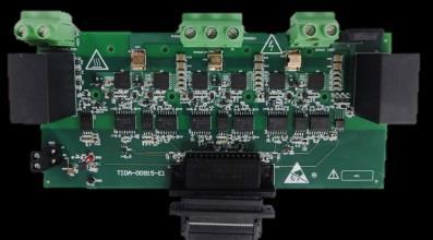
23 TIDA Test Results Efficiency and Thermal Test Setup TIDA PCB Top Side with LMG3410 PMSM Servo Motor TIDA PCB bottom Side w/ Heatsink C2000 Control Board Cabling to Power Analyzer 23
24 TIDA Test Results Power Loss and Efficiency Results Output power up to 2kW, output phase current up to 4.5A RMS Power Losses vs. Phase Current Efficiency vs. Phase Current / Output Power Peak Efficiency >98% at 100kHz! Efficiency >99% at 24kHz! V DC Link = 300V Fastest Transient is During Hard Switching Dead band = 50nS Output Power (Watts) P out = x I 24


25 TIDA Test Results Thermal Analysis at 23C Ambient 100kHz PWM, 4.5A RMS output current PCB Top Side LMG3410 PCB Bottom Side: Heat Sink 25
26 High Performance Reinforced Isolated In- Phase Current Sensing 26
27 Motor Current Sensing Why motor current feedback is needed: Torque control (e.g. FOC algorithm) Motor short circuit protection Motor power monitoring Derating current output based on module temperature Motor health diagnostics Key motor parameters which are used to diagnose motor health are calculated from motor current Short in load Miss wiring or load short circuit S 1 S 3 S 5 Induction motor torque, T α ФI 2 cosф 2 PMSM motor torque, T α ФI Inverter output power, P = 3VIcosФ Ground fault Miss wiring or dielectric breakdown S 1 S 3 S 5 i a i a DC i b i c DC i b i c S 2 S 4 S 6 S 2 S 4 S 6 27
28 Where to Sense Motor Current Location of Current Sensing: 1) Low-Side Current Sensing 1 Most common due to cost and common GND Multiple configurations based on accuracy desired Single shunt, two shunt or three shunt resistors Discontinuous current, exact timing is critical V Bus+ 3 High-Side 2) In-Line Phase Current Sensing 2 Most accurate High common mode, often Isolation required Continuous current measurement In-Line 2 TI Dave s Control Center 3) High-Side Current Sensing 3 Isolation required especially for higher voltage Generally used to detect shoot through and GND fault currents Typically not used w/ 3-phase AC drives V Bus- Low-Side 1 28
29 Phase Current and Voltage During PWM DC+ 5 PWM Isolated Gate Driver 320V DC.... >1000V DC 2 1 V L1(Phase to DC-) I L1(Phase) high dv/dt ~1..10 kv/us (typ. IGBT) 6 PWM DC- Isolated Gate Driver 3 4 I LowSide V LowSide Key Design Challenges Accurate, high-resolution, low-latency phase current sensing Lowest latency over-current, short-circuit detection Isolation and EMC immunity (electrical fast transients, CMTI, surge) 5 6 PWM, e.g. 16kHz 29
")
30 Traditional Analog Current Measurement Techniques Example: Hall or Fluxgate based Current Transducer with Galvanic Isolation Phase current hot side Phase current equivalent voltage cold side Each stage adds error Typically <10 bit accuracy on system level V OUT typical 12-bit, SPI or parallel interface Galvanic isolated closed-loop current transducer +i MAX - i MAX Current thresholds (+/-) typically set by DAC (programmable) S/H Window comparator SAR ADC typical latency <2us typical latency <<1us Phase current (digital) additional latency through digital interface (e.g. SPI) OC PWM trip 30
31 Limitation of Analog Isolation and SAR ADC Sensor: Linearity, drift and bandwidth of magnetic based current transducers (galvanic isolation) typically lower performance than shunt based current sensor Analog isolation (analog signal on secondary side) more susceptible to noise than a digital signal Analog IC: For higher than 12-bit resolution cost for analog signal chain increases over-proportionally Analog IC/system: Typical single sampling at PWM period Therefore typically requires higher order analog low-pass filter (amplifier) to meet Nyquist theorem Hence more sensitive to noise at sample time Analog system: Additional latency due to multiple conversion stages 31


32 Isolated Delta Sigma Modulator Capacitive Isolation barrier 100 kv/μs CMTI 5000 Vrms Isolation for 1 min per UL1577 Input 0 V Bit stream 1 and 0 high for 50% of time Input +FS Bit stream 1 and 0 high for % of time Input FS Bit stream 1 and 0 high for % of time ±250 mv and ±50 mv analog input voltage range options On-off keying Clock frequency up to 21 MHz Input to isolation channel Carrier signal across isolation barrier Output of isolation channel 32
33 Isolated Delta Sigma Modulator Signal Chain Single external digital signal path for both current sensing and short circuit detection Shunt resistor more linear, higher bandwidth and lower drift over temperature Digital signal less immune to noise single conversion stage! All processing in digital domain! >14 bit accuracy on system level! CMOS output or Manchester coded CMOS output 33

34 SINC Filtering SINC1 filter is a moving average filter. SINC2 and SINC3 are higher order filters using cascaded SINC1 filters H Z = 1 Z OSR 1 Z 1 M OSR: Oversampling ratio M: SINC filter order f S : Modulator clock frequency f DATA = f S /OSR Decimated data rate 34
35 SINC Filter Window Placement SINC 1/2/3 Weighing Factors vs OSR 1/OSR SINC1 SINC2 Blue Weighing Factor SINC3 PHASE CURRENT Center PWM Filter Window synchronized to center of PWM OSR 2 x OSR 3 x OSR Delta Sigma Modulator Samples PWM SINC filter weighing factors SINC filter window placement 35

36 Reinforced isolated in-phase current sensing design with delta sigma modulators TIDA High accuracy and low drift: Calibrated full scale accuracy of <0.5% across temperature range of 0C to 55C High CMTI of modulator improves noise immunity to switching transients. Loss of secondary power detect with fail safe output Small pin count (8) enables compact solution Simplified clock routing to delta sigma modulators due to Manchester encoded data output Short circuit response time less than 1.5 µs 36


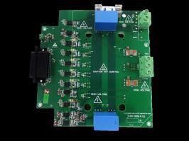
37 Board Picture top and bottom view 37


38 Isolation Barrier, Connection to Heat Sink 38
39 CMOS Output Version Different clock and data line lengths (propagation delays) may cause setup and hold time issues at the MCU Possibility of signal integrity problems due to star routing of clock signal from control board to power board Makes clock termination difficult Need additional clock buffer IC on power board to avoid signal integrity problems 39
40 Manchester Coded CMOS Output Version DATA CLOCK Manchester Encoded data = CLOCK (XOR) DATA Manchester coded data is self synchronizing Data can be AC coupled Clock Source Advantages of Manchester encoding: No setup/hold time concerns Easy (series) clock termination No clock signal required at the MCU Reduced and easier wiring efforts as clock signal is not required to be sent across the boards 40


41 Test setup for Current Measurement Accuracy Testing 41
42 Current Measurement Accuracy SINC3 filter 256 OSR Precise measurements Calibrated FSR error < C, 4kHz PWM, SINC 3 filter, 256 OSR AMC1306 output reading in Amperes % FSR Error vs average phase current High linearity Motor Phase Current (A) Effect of temperature variation is very low Absolute error vs average phase current at different temperatures 42
43 Response Time to Short Circuit Detection Response time, t r = n OSR n is the order of SINC filter OSR is the oversampling ratio of ΔΣ filter module Fs is the modulator clock frequency ( 20 MHz) f s Fast short-circuit protection is required to protect motor and inverter power stage IGBT s required to be switched off within ~ 4 µs on short detection Filter order O S R Current measurement resolution for FSR of 80 Apk Response time SINC A 1.2 μs SINC A 1.2 μs SINC A 1.2 μs Input voltage step tr = 1.32 µs Output short indication Short current detection threshold has been set at ± 40 Apk for the test result SINC3, OSR 8 43

44 Loss of Secondary Power Detection If due to fault in ΔΣ modulator analog power supply (AVDD) it becomes zero. The output of the modulator is not defined and may cause system malfunctions. AMC1306 implements fail safe output and common mode overvoltage indication 44

45 Input Exceeding Full Scale Range If input full scale voltage measurement range (± 320 mv) is exceeded AMC1306 implements a 1 or 0 every 128 th bit depending on the polarity of the signal being sensed. 45
46 Thank you for your attention References: TI Designs showing isolated in-phase current sensing using ΔΣ modulators: TIDA TIDA TIDA More on ΔΣ modulators How Delta Sigma ADC's Work, Part 1 How Delta Sigma ADC's Work, Part 2 Digital Filter Types in Delta-Sigma ADCs High Precision in motor drive control enables industrial advances TI Designs with GaN Modules: TIDA TIDA TIDA More on TI s GaN Technology Direct-drive configuration for GaN devices Optimizing GaN performance with an integrated driver GaN FET module performance advantage over silicon High Voltage Half Bridge Design Guide for LMG3410 Smart GaN Speed your time to market with Motor drive TI Designs Find reference block diagrams for Motor drive Systems Check out our Motor Drive technical documents 46
Designing reliable and high density power solutions with GaN. Created by: Masoud Beheshti Presented by: Paul L Brohlin
 Designing reliable and high density power solutions with GaN Created by: Masoud Beheshti Presented by: Paul L Brohlin What will I get out of this presentation? Why GaN? Integration for System Performance
Designing High density Power Solutions with GaN Created by: Masoud Beheshti Presented by: Xaver Arbinger
 Designing High density Power Solutions with GaN Created by: Masoud Beheshti Presented by: Xaver Arbinger Topics Why GaN? Integration for Higher System Performance Application Examples Taking GaN beyond
Get Your GaN PhD in Less Than 60 Minutes!
 Get Your GaN PhD in Less Than 60 Minutes! 1 Detailed agenda Why is GaN Exciting GaN Fundamentals Cost and Reliability Totem Pole PFC Isolated LLC Motor Drive LiDAR Driving GaN Choosing a GaN Tools 4 Why
GaN in Practical Applications
 in Practical Applications 1 CCM Totem Pole PFC 2 PFC: applications and topology Typical AC/DC PSU 85-265 V AC 400V DC for industrial, medical, PFC LLC 12, 24, 48V DC telecomm and server applications. PFC
Power of GaN. Enabling designers to create smaller, more efficient and higher-performing AC/DC power supplies
 Power of GaN Enabling designers to create smaller, more efficient and higher-performing AC/DC power supplies Steve Tom Product Line Manager, GaN Products stom@ti.com Solving power and energy-management
Gate Drive Optimisation
 Gate Drive Optimisation 1. Background Driving of gates of MOSFET, IGBT and SiC/GaN switching devices is a fundamental requirement in power conversion. In the case of ground-referenced drives this is relatively
IAP200T120 SixPac 200A / 1200V 3-Phase Bridge IGBT Inverter
 Configurable Power FEATURES INCLUDE Multi-Function Power Assembly Compact Size 9 H X 17.60 W X 11.00 D DC Bus Voltages to 850VDC Snubber-less operation to 650VDC Switching frequencies to over 20kHz Protective
Using Optical Isolation Amplifiers in Power Inverters for Voltage, Current and Temperature Sensing
 Using Optical Isolation Amplifiers in Power Inverters for Voltage, Current and Temperature Sensing by Hong Lei Chen, Product Manager, Avago Technologies Abstract Many industrial equipments and home appliances
EUP V/12V Synchronous Buck PWM Controller DESCRIPTION FEATURES APPLICATIONS. Typical Application Circuit. 1
 5V/12V Synchronous Buck PWM Controller DESCRIPTION The is a high efficiency, fixed 300kHz frequency, voltage mode, synchronous PWM controller. The device drives two low cost N-channel MOSFETs and is designed
Features: Phase A Phase B Phase C -DC_A -DC_B -DC_C
 Three Phase Inverter Power Stage Description: The SixPac TM from Applied Power Systems is a configurable IGBT based power stage that is configured as a three-phase bridge inverter for motor control, power
TENTATIVE PP225D120. POW-R-PAK TM 225A / 1200V Half Bridge IGBT Assembly. Description:
 Description: The Powerex is a configurable IGBT based power assembly that may be used as a converter, chopper, half or full bridge, or three phase inverter for motor control, power supply, UPS or other
Designing Reliable and High-Density Power Solutions with GaN
 Designing Reliable and High-Density Power Solutions with GaN 1 Detailed agenda Why is GaN Exciting GaN Fundamentals Cost and Reliability Totem Pole PFC Isolated LLC Motor Drive LiDAR Driving GaN Choosing
IR3101 Series 1.6A, 500V
 Half-Bridge FredFet and Integrated Driver Features Output power FredFets in half-bridge configuration High side gate drive designed for bootstrap operation Bootstrap diode integrated into package. Lower
FSB50760SF, FSB50760SFT Motion SPM 5 SuperFET Series
 FSB50760SF, FSB50760SFT Motion SPM 5 SuperFET Series Features UL Certified No. E209204 (UL1557) 600 V R DS(on) = 530 m Max SuperFET MOSFET 3- Phase with Gate Drivers and Protection Built-in Bootstrap Diodes
Technical. Application. Assembly. Availability. Pricing. Phone
 6121 Baker Road, Suite 108 Minnetonka, MN 55345 www.chtechnology.com Phone (952) 933-6190 Fax (952) 933-6223 1-800-274-4284 Thank you for downloading this document from C&H Technology, Inc. Please contact
TENTATIVE PP800D120-V01
 Description: The Powerex POW-R-PAK is a configurable IGBT based power assembly that may be used as a converter, chopper, half or full bridge, or three phase inverter for motor control, power supply, UPS
GS61008P Bottom-side cooled 100 V E-mode GaN transistor Preliminary Datasheet
 Features 100 V enhancement mode power switch Bottom-side cooled configuration R DS(on) = 7 mω I DS(max) = 90 A Ultra-low FOM Island Technology die Low inductance GaNPX package Easy gate drive requirements
FSB50250AS Motion SPM 5 Series
 FSB50250AS Motion SPM 5 Series Features UL Certified No. E209204 (UL1557) 500 V R DS(on) = 3.8 Max FRFET MOSFET 3-Phase Inverter with Gate Drivers and Protection Built-In Bootstrap Diodes Simplify PCB
GS61008T Top-side cooled 100 V E-mode GaN transistor Preliminary Datasheet
 Features 100 V enhancement mode power switch Top-side cooled configuration R DS(on) = 7 mω I DS(max) = 90 A Ultra-low FOM Island Technology die Low inductance GaNPX package Easy gate drive requirements
FSB50450UD Motion SPM 5 Series
 FSB50450UD Motion SPM 5 Series Features UL Certified No. E209204 (UL1557) 500 V R DS(on) = 2.4 Max FRFET MOSFET 3-Phase Inverter with Gate Drivers and Protection Built-In Bootstrap Diodes Simplify PCB
FSB50450S Motion SPM 5 Series
 FSB50450S Motion SPM 5 Series Features UL Certified No. E209204 (UL1557) 500 V R DS(on) = 2.4 Max FRFET MOSFET 3-Phase Inverter with Gate Drivers Separate Open-Source Pins from Low-Side MOSFETs for Three-Phase
The Quest for High Power Density
 The Quest for High Power Density Welcome to the GaN Era Power Conversion Technology Drivers Key design objectives across all applications: High power density High efficiency High reliability Low cost 2
Appendix: Power Loss Calculation
 Appendix: Power Loss Calculation Current flow paths in a synchronous buck converter during on and off phases are illustrated in Fig. 1. It has to be noticed that following parameters are interrelated:
Unlocking the Power of GaN PSMA Semiconductor Committee Industry Session
 Unlocking the Power of GaN PSMA Semiconductor Committee Industry Session March 24 th 2016 Dan Kinzer, COO/CTO dan.kinzer@navitassemi.com 1 Mobility (cm 2 /Vs) EBR Field (MV/cm) GaN vs. Si WBG GaN material
CHAPTER 7 HARDWARE IMPLEMENTATION
 168 CHAPTER 7 HARDWARE IMPLEMENTATION 7.1 OVERVIEW In the previous chapters discussed about the design and simulation of Discrete controller for ZVS Buck, Interleaved Boost, Buck-Boost, Double Frequency
GS P Bottom-side cooled 100 V E-mode GaN transistor Preliminary Datasheet. Features. Applications. Description.
 Features 100 V enhancement mode power switch Bottom-side cooled configuration R DS(on) = 5 mω I DS(max) = 120 A Ultra-low FOM Island Technology die Low inductance GaNPX package Easy gate drive requirements
235 W Maximum Power Dissipation (whole module) 470 T J Junction Operating Temperature -40 to 150. Torque strength
 470 T J Junction Operating Temperature -40 to 150. Torque strength") Discontinued PRODUCT SUMMARY (TYPICAL) V DS (V) 600 R DS(on) (m ) 30 GaN Power Hybrid HEMT Half-Bridge Module Features High frequency operation Free-wheeling diode not required Applications Compact DC-DC
Discontinued PRODUCT SUMMARY (TYPICAL) V DS (V) 600 R DS(on) (m ) 30 GaN Power Hybrid HEMT Half-Bridge Module Features High frequency operation Free-wheeling diode not required Applications Compact DC-DC
POWER DELIVERY SYSTEMS
 www.silabs.com Smart. Connected. Energy-Friendly. CMOS ISOLATED GATE S ENHANCE POWER DELIVERY SYSTEMS CMOS Isolated Gate Drivers (ISOdrivers) Enhance Power Delivery Systems Fully integrated isolated gate
GaN Transistors for Efficient Power Conversion
 GaN Transistors for Efficient Power Conversion Agenda How GaN works Electrical Characteristics Design Basics Design Examples Summary 2 2 How GaN Works 3 3 The Ideal Power Switch Block Infinite Voltage
SPECIAL REPORT: RENEWABLE ENERGY (PG29) January/February 2012
 January/February 2012") SPECIAL REPORT: RENEWABLE ENERGY (PG29) January/February 2012 POWER SYSTEMS DESIGN JANUARY/FEBRUARY 2012 ISOLATED μmodule POWER CONVERTER Improving Signal Measurement Accuracy By Willie Chan Properly implemented,
SPECIAL REPORT: RENEWABLE ENERGY (PG29) January/February 2012 POWER SYSTEMS DESIGN JANUARY/FEBRUARY 2012 ISOLATED μmodule POWER CONVERTER Improving Signal Measurement Accuracy By Willie Chan Properly implemented,
GS61004B 100V enhancement mode GaN transistor Preliminary Datasheet
 Features 100V enhancement mode power switch Bottom-side cooled configuration R DS(on) = 15 mω I DS(max) = 45 A Ultra-low FOM Island Technology die Low inductance GaNPX package Easy gate drive requirements
IAP200B120 Integrated Advanced PowerStack 200A / 1200V Full-Bridge IGBT Inverter
 FEATURES INCLUDE Multi-Function Power Assembly Compact Size 8 H X 17.6 W X 11. D DC Bus Voltages to 85VDC Snubber-less operation to 65VDC Switching frequencies to over 2kHz Protective circuitry with fail-safe
Features MIC2193BM. Si9803 ( 2) 6.3V ( 2) VDD OUTP COMP OUTN. Si9804 ( 2) Adjustable Output Synchronous Buck Converter
 6.3V ( 2) VDD OUTP COMP OUTN. Si9804 ( 2) Adjustable Output Synchronous Buck Converter") MIC2193 4kHz SO-8 Synchronous Buck Control IC General Description s MIC2193 is a high efficiency, PWM synchronous buck control IC housed in the SO-8 package. Its 2.9V to 14V input voltage range allows
MIC2193 4kHz SO-8 Synchronous Buck Control IC General Description s MIC2193 is a high efficiency, PWM synchronous buck control IC housed in the SO-8 package. Its 2.9V to 14V input voltage range allows
HIGH SPEED, 100V, SELF OSCILLATING 50% DUTY CYCLE, HALF-BRIDGE DRIVER
 Data Sheet No. 60206 HIGH SPEED, 100V, SELF OSCILLATING 50% DUTY CYCLE, HALF-BRIDGE DRIVER Features Simple primary side control solution to enable half-bridge DC-Bus Converters for 48V distributed systems
TPH3207WS TPH3207WS. GaN Power Low-loss Switch PRODUCT SUMMARY (TYPICAL) Absolute Maximum Ratings (T C =25 C unless otherwise stated)
 Absolute Maximum Ratings (T C =25 C unless otherwise stated)") PRODUCT SUMMARY (TYPICAL) V DS (V) 650 R DS(on) (m ) 35 Q rr (nc) 175 Features Low Q rr Free-wheeling diode not required Quiet Tab for reduced EMI at high dv/dt GSD pin layout improves high speed design
PRODUCT SUMMARY (TYPICAL) V DS (V) 650 R DS(on) (m ) 35 Q rr (nc) 175 Features Low Q rr Free-wheeling diode not required Quiet Tab for reduced EMI at high dv/dt GSD pin layout improves high speed design
IAP100T120 Integrated Advanced PowerStack 100A / 1200V Three-Phase-Bridge IGBT Inverter
 FEATURES INCLUDE Compact Size 8.00 H X 17.56 W X 11.00 D DC Bus Voltages to 850VDC Snubber-less operation to 650VDC Switching frequencies to over 20kHz Protective circuitry with fail-safe opto-isolated
GS66516T Top-side cooled 650 V E-mode GaN transistor Preliminary Datasheet
 Features 650 V enhancement mode power switch Top-side cooled configuration R DS(on) = 25 mω I DS(max) = 60 A Ultra-low FOM Island Technology die Low inductance GaNPX package Easy gate drive requirements
PP400B060-ND. H-Bridge POW-R-PAK IGBT Assembly 400 Amperes/600 Volts
 Powerex, Inc., 173 Pavilion Lane, Youngwood, Pennsylvania 15697 (724) 925-7272 www.pwrx.com H-Bridge POW-R-PAK IGBT Assembly Q Q J P (8 PLACES) +DC C2E1 R (2 PLACES) PIN 1 N U B M N F DC L (6 PLACES) G
Motion-SPM. FSB50550UTD Smart Power Module (SPM ) General Description. Features. Absolute Maximum Ratings. Symbol Parameter Conditions Rating Units
 General Description. Features. Absolute Maximum Ratings. Symbol Parameter Conditions Rating Units") FSB50550UTD Smart Power Module (SPM ) Features 500V R DS(on) =1.4W(max) 3-phase FRFET inverter including high voltage integrated circuit (HVIC) 3 divided negative dc-link terminals for inverter current
FSB50550UTD Smart Power Module (SPM ) Features 500V R DS(on) =1.4W(max) 3-phase FRFET inverter including high voltage integrated circuit (HVIC) 3 divided negative dc-link terminals for inverter current
Fig. 1 - Enhancement mode GaN has a circuiut schematic similar to silicon MOSFETs with Gate (G), Drain (D), and Source (S).
, Drain (D), and Source (S).") GaN Basics: FAQs Sam Davis; Power Electronics Wed, 2013-10-02 Gallium nitride transistors have emerged as a high-performance alternative to silicon-based transistors, thanks to the technology's ability
GaN Basics: FAQs Sam Davis; Power Electronics Wed, 2013-10-02 Gallium nitride transistors have emerged as a high-performance alternative to silicon-based transistors, thanks to the technology's ability
GS61008P Bottom-side cooled 100 V E-mode GaN transistor Preliminary Datasheet. Features. Applications. Description. Circuit Symbol.
 Features 100 V enhancement mode power switch Bottom-side cooled configuration R DS(on) = 7 mω I DS(max) = 90 A Ultra-low FOM Island Technology die Low inductance GaNPX package Easy gate drive requirements
PowerAmp Design. PowerAmp Design PAD112 HIGH VOLTAGE OPERATIONAL AMPLIFIER
 PowerAmp Design Rev C KEY FEATURES LOW COST HIGH VOLTAGE 150 VOLTS HIGH OUTPUT CURRENT 5 AMPS 50 WATT DISSIPATION CAPABILITY 100 WATT OUTPUT CAPABILITY INTEGRATED HEAT SINK AND FAN COMPATIBLE WITH PAD123
GS61008T Top-side cooled 100 V E-mode GaN transistor Preliminary Datasheet
 Features 100 V enhancement mode power switch Top-side cooled configuration R DS(on) = 7 mω I DS(max) = 90 A Ultra-low FOM Island Technology die Low inductance GaNPX package Easy gate drive requirements
SA60. H-Bridge Motor Driver/Amplifiers SA60
 H-Bridge Motor Driver/Amplifiers FEATURES LOW COSOMPLETE H-BRIDGE SELF-CONTAINED SMART LOWSIDE/ HIGHSIDE DRIVE CIRCUITRY WIDE SUPPLY RANGE: UP TO 8V A CONTINUOUS OUTPUT ISOLATED CASE ALLOWS DIRECT HEATSINKING
Motion-SPM. FSB50250UD Smart Power Module (SPM ) General Description. Features. Absolute Maximum Ratings. Symbol Parameter Conditions Rating Units
 General Description. Features. Absolute Maximum Ratings. Symbol Parameter Conditions Rating Units") FSB50250UD Smart Power Module (SPM ) Features 500V R DS(on) =4.2W(max) 3-phase FRFET inverter including high voltage integrated circuit (HVIC) 3 divided negative dc-link terminals for inverter current
FSB50250UD Smart Power Module (SPM ) Features 500V R DS(on) =4.2W(max) 3-phase FRFET inverter including high voltage integrated circuit (HVIC) 3 divided negative dc-link terminals for inverter current
Designing a 99% Efficient Totem Pole PFC with GaN. Serkan Dusmez, Systems and applications engineer
 Designing a 99% Efficient Totem Pole PFC with GaN Serkan Dusmez, Systems and applications engineer 1 What will I get out of this session? Purpose: Why GaN Based Totem-pole PFC? Design guidelines for getting
Application Note 5121
 Isolation Amplifiers and Hall-Effect Device For Motor Control Current Sensing Applications Application Note 5121 Introduction Current Sensor is an essential component in a motor control system. Recent
FSFR-XS Series Fairchild Power Switch (FPS ) for Half-Bridge Resonant Converters
 for Half-Bridge Resonant Converters") February 203 FSFR-XS Series Fairchild Power Switch (FPS ) for Half-Bridge Resonant Converters Features Variable Frequency Control with 50% Duty Cycle for Half-Bridge Resonant Converter Topology High Efficiency
February 203 FSFR-XS Series Fairchild Power Switch (FPS ) for Half-Bridge Resonant Converters Features Variable Frequency Control with 50% Duty Cycle for Half-Bridge Resonant Converter Topology High Efficiency
GS61004B 100V enhancement mode GaN transistor Preliminary Datasheet
 Features 100V enhancement mode power switch Bottom-side cooled configuration R DS(on) = 15 mω I DS(max) = 45 A Ultra-low FOM Island Technology die Low inductance GaNPX package Easy gate drive requirements
PC Krause and Associates, Inc.
 Common-mode challenges in high-frequency switching converters 14 NOV 2016 Nicholas Benavides, Ph.D. (Sr. Lead Engineer) 3000 Kent Ave., Suite C1-100 West Lafayette, IN 47906 (765) 464-8997 (Office) (765)
PowerAmp Design. PowerAmp Design PAD117A RAIL TO RAIL OPERATIONAL AMPLIFIER
 PowerAmp Design RAIL TO RAIL OPERATIONAL AMPLIFIER Rev J KEY FEATURES LOW COST RAIL TO RAIL INPUT & OUTPUT SINGLE SUPPLY OPERATION HIGH VOLTAGE 100 VOLTS HIGH OUTPUT CURRENT 15A 250 WATT OUTPUT CAPABILITY
A Solution to Simplify 60A Multiphase Designs By John Lambert & Chris Bull, International Rectifier, USA
 A Solution to Simplify 60A Multiphase Designs By John Lambert & Chris Bull, International Rectifier, USA As presented at PCIM 2001 Today s servers and high-end desktop computer CPUs require peak currents
LF411 Low Offset, Low Drift JFET Input Operational Amplifier
 Low Offset, Low Drift JFET Input Operational Amplifier General Description These devices are low cost, high speed, JFET input operational amplifiers with very low input offset voltage and guaranteed input
LM2462 Monolithic Triple 3 ns CRT Driver
 LM2462 Monolithic Triple 3 ns CRT Driver General Description The LM2462 is an integrated high voltage CRT driver circuit designed for use in color monitor applications. The IC contains three high input
75 VOLT 8 AMP MOSFET H-BRIDGE PWM MOTOR DRIVER/AMPLIFIER
 M.S.KENNEDY CORP. 75 OLT 8 AMP MOSFET HBRIDGE PWM MOTOR DRIER/AMPLIFIER 4707 Dey Road Liverpool, N.Y. 088 (5) 70675 FEATURES: Low Cost Complete HBridge 8 Amp Capability, 75 olt Maximum Rating Selfcontained
75 VOLT 10 AMP MOSFET H-BRIDGE PWM MOTOR DRIVER/AMPLIFIER
 M.S.KENNEDY CORP. ISO 900 CERTIFIED BY DESC 75 OLT 0 AMP MOSFET 4 HBRIDGE PWM MOTOR DRIER/AMPLIFIER 4707 Dey Road Liverpool, N.Y. 3088 (35) 70675 FEATURES: Low Cost Complete HBridge 0 Amp Capability, 75
Constant Current Switching Regulator for White LED
 Constant Current Switching Regulator for White LED FP7201 General Description The FP7201 is a Boost DC-DC converter specifically designed to drive white LEDs with constant current. The device can support
Description. Operating Temperature Range
 FAN7393 Half-Bridge Gate Drive IC Features Floating Channel for Bootstrap Operation to +6V Typically 2.5A/2.5A Sourcing/Sinking Current Driving Capability Extended Allowable Negative V S Swing to -9.8V
Symbol Parameter Typical
 PRODUCT SUMMARY (TYPICAL) V DS (V) 650 R DS(on) (m ) 110 Q rr (nc) 54 Features Low Q rr Free-wheeling diode not required Low-side Quiet Tab for reduced EMI RoHS compliant High frequency operation Applications
FAN2013 2A Low-Voltage, Current-Mode Synchronous PWM Buck Regulator
 FAN2013 2A Low-Voltage, Current-Mode Synchronous PWM Buck Regulator Features 95% Efficiency, Synchronous Operation Adjustable Output Voltage from 0.8V to V IN-1 4.5V to 5.5V Input Voltage Range Up to 2A
AN Analog Power USA Applications Department
 Using MOSFETs for Synchronous Rectification The use of MOSFETs to replace diodes to reduce the voltage drop and hence increase efficiency in DC DC conversion circuits is a concept that is widely used due
Enhancing Power Delivery System Designs with CMOS-Based Isolated Gate Drivers
 Enhancing Power Delivery System Designs with CMOS-Based Isolated Gate Drivers Fully-integrated isolated gate drivers can significantly increase the efficiency, performance and reliability of switch-mode
LM2412 Monolithic Triple 2.8 ns CRT Driver
 Monolithic Triple 2.8 ns CRT Driver General Description The is an integrated high voltage CRT driver circuit designed for use in high resolution color monitor applications. The IC contains three high input
PowerAmp Design. PowerAmp Design PAD20 COMPACT HIGH VOLTAGE OP AMP
 PowerAmp Design Rev C KEY FEATURES LOW COST HIGH VOLTAGE 150 VOLTS HIGH OUTPUT CURRENT 5A 40 WATT DISSIPATION CAPABILITY 80 WATT OUTPUT CAPABILITY INTEGRATED HEAT SINK AND FAN SMALL SIZE 40mm SQUARE RoHS
AC-DC SMPS: Up to 15W Application Solutions
 AC-DC SMPS: Up to 15W Application Solutions Yehui Han Applications Engineer April 2017 Agenda 2 Introduction Flyback Topology Optimization Buck Topology Optimization Layout and EMI Optimization edesignsuite
Analog I/O. ECE 153B Sensor & Peripheral Interface Design Winter 2016
 Analog I/O ECE 153B Sensor & Peripheral Interface Design Introduction Anytime we need to monitor or control analog signals with a digital system, we require analogto-digital (ADC) and digital-to-analog
Integrated Power Hybrid IC for Appliance Motor Drive Applications
 Integrated Power Hybrid IC for Appliance Motor Drive Applications PD-97277 Rev A IRAM336-025SB Series 3 Phase Inverter HIC 2A, 500V Description International Rectifier s IRAM336-025SB is a multi-chip Hybrid
LD /01/2013. Boost Controller for LED Backlight. General Description. Features. Applications. Typical Application REV: 00
 04/01/2013 Boost Controller for LED Backlight REV: 00 General Description The LD5861 is a wide-input asynchronous current mode boost controller, capable to operate in the range between 9V and 28V and to
MPM V-5.5V, 4A, Power Module, Synchronous Step-Down Converter with Integrated Inductor
 The Future of Analog IC Technology MPM3840 2.8V-5.5V, 4A, Power Module, Synchronous Step-Down Converter with Integrated Inductor DESCRIPTION The MPM3840 is a DC/DC module that includes a monolithic, step-down,
10A Current Mode Non-Synchronous PWM Boost Converter
 10A Current Mode Non-Synchronous PWM Boost Converter General Description The is a current mode boost DC-DC converter. It is PWM circuitry with built-in 15mΩ power MOSFET make this regulator highly power
FBA42060 PFC SPM 45 Series for Single-Phase Boost PFC
 FBA42060 PFC SPM 45 Series for Single-Phase Boost PFC Features UL Certified No. E209204 (UL1557) 600 V - 20 A Single-Phase Boost PFC with Integral Gate Driver and Protection Low Thermal Resistance Using
GaN is Crushing Silicon. EPC - The Leader in GaN Technology IEEE PELS
 GaN is Crushing Silicon EPC - The Leader in GaN Technology IEEE PELS 2014 www.epc-co.com 1 Agenda How egan FETs work Hard Switched DC-DC converters High Efficiency point-of-load converter Envelope Tracking
Features MIC2194BM VIN EN/ UVLO CS OUTP VDD FB. 2k COMP GND. Adjustable Output Buck Converter MIC2194BM UVLO
 MIC2194 400kHz SO-8 Buck Control IC General Description s MIC2194 is a high efficiency PWM buck control IC housed in the SO-8 package. Its 2.9V to 14V input voltage range allows it to efficiently step
Unleash SiC MOSFETs Extract the Best Performance
 Unleash SiC MOSFETs Extract the Best Performance Xuning Zhang, Gin Sheh, Levi Gant and Sujit Banerjee Monolith Semiconductor Inc. 1 Outline SiC devices performance advantages Accurate test & measurement
PCB layout guidelines. From the IGBT team at IR September 2012
 PCB layout guidelines From the IGBT team at IR September 2012 1 PCB layout and parasitics Parasitics (unwanted L, R, C) have much influence on switching waveforms and losses. The IGBT itself has its own
GS66508T Top-side cooled 650 V E-mode GaN transistor Preliminary Datasheet
 Features 650 V enhancement mode power switch Top-side cooled configuration R DS(on) = 50 mω I DS(max) = 30 A Ultra-low FOM Island Technology die Low inductance GaNPX package Easy gate drive requirements
GaN Power ICs: Integration Drives Performance
 GaN Power ICs: Integration Drives Performance Stephen Oliver, VP Sales & Marketing stephen.oliver@navitassemi.com Bodo s Power Conference, Munich December 5 th, 2017 Navitas Semiconductor Inc. World s
GS66502B Bottom-side cooled 650 V E-mode GaN transistor Preliminary Datasheet
 GS66502B Features 650 V enhancement mode power switch Bottom-side cooled configuration R DS(on) = 200 mω I DS(max) = 7.5 A Ultra-low FOM Island Technology die Low inductance GaNPX package Easy gate drive
23V 3A Step-Down DC/DC Converter
 23V 3A Step-Down DC/DC Converter FEATURES 3A Continuous Output Current Programmable Soft Start 100mΩ Internal Power MOSFET Switch Stable with Low ESR Output Ceramic Capacitors Up to 95% Efficiency 22µA
SiC Transistor Basics: FAQs
 SiC Transistor Basics: FAQs Silicon Carbide (SiC) MOSFETs exhibit higher blocking voltage, lower on state resistance and higher thermal conductivity than their silicon counterparts. Oct. 9, 2013 Sam Davis
MIC2196. Features. General Description. Applications. Typical Application. 400kHz SO-8 Boost Control IC
 400kHz SO-8 Boost Control IC General Description Micrel s is a high efficiency PWM boost control IC housed in a SO-8 package. The is optimized for low input voltage applications. With its wide input voltage
MAXREFDES121# Isolated 24V to 3.3V 33W Power Supply
 System Board 6309 MAXREFDES121# Isolated 24V to 3.3V 33W Power Supply Maxim s power-supply experts have designed and built a series of isolated, industrial power-supply reference designs. Each of these
UF3C120080K4S. 1200V-80mW SiC Cascode DATASHEET. Description. Features. Typical applications CASE D (1) CASE G (4) KS (3) S (2) Rev.
 CASE G (4) KS (3) S (2) Rev.") 1V-8mW SiC Cascode Rev. A, January 19 DATASHEET UF3C18K4S CASE CASE D (1) Description United Silicon Carbide's cascode products co-package its highperformance F3 SiC fast JFETs with a cascode optimized
1V-8mW SiC Cascode Rev. A, January 19 DATASHEET UF3C18K4S CASE CASE D (1) Description United Silicon Carbide's cascode products co-package its highperformance F3 SiC fast JFETs with a cascode optimized
AIC1340 High Performance, Triple-Output, Auto- Tracking Combo Controller
 High Performance, Triple-Output, Auto- Tracking Combo Controller FEATURES Provide Triple Accurate Regulated Voltages Optimized Voltage-Mode PWM Control Dual N-Channel MOSFET Synchronous Drivers Fast Transient
MLX83100 Automotive DC Pre-Driver EVB83100 for Brushed DC Applications with MLX83100
 EVB83100 for Brushed DC Applications with MLX83100 Stefan Poels JULY 17, 2017 VAT BE 0435.604.729 Transportstraat 1 3980 Tessenderlo Phone: +32 13 67 07 95 Mobile: +32 491 15 74 18 Fax: +32 13 67 07 70
GS66506T Top-side cooled 650 V E-mode GaN transistor Preliminary Datasheet
 Features 650 V enhancement mode power switch Top-side cooled configuration R DS(on) = 67 mω I DS(max) = 22.5 A Ultra-low FOM Island Technology die Low inductance GaNPX package Easy gate drive requirements
ACT111A. 4.8V to 30V Input, 1.5A LED Driver with Dimming Control GENERAL DESCRIPTION FEATURES APPLICATIONS TYPICAL APPLICATION CIRCUIT
 4.8V to 30V Input, 1.5A LED Driver with Dimming Control FEATURES Up to 92% Efficiency Wide 4.8V to 30V Input Voltage Range 100mV Low Feedback Voltage 1.5A High Output Capacity PWM Dimming 10kHz Maximum
High Efficiency 8A Synchronous Boost Convertor
 High Efficiency 8A Synchronous Boost Convertor General Description The is a synchronous current mode boost DC-DC converter. Its PWM circuitry with built-in 8A current power MOSFET makes this converter
FAN MHz TinyBoost Regulator with 33V Integrated FET Switch
 FAN5336 1.5MHz TinyBoost Regulator with 33V Integrated FET Switch Features 1.5MHz Switching Frequency Low Noise Adjustable Output Voltage Up to 1.5A Peak Switch Current Low Shutdown Current:
GS66516B Bottom-side cooled 650 V E-mode GaN transistor Preliminary Datasheet
 Features 650 V enhancement mode power switch Bottom-side cooled configuration R DS(on) = 25 mω I DS(max) = 60 A Ultra-low FOM Island Technology die Low inductance GaNPX package Easy gate drive requirements
1.5MHz, 3A Synchronous Step-Down Regulator
 1.5MHz, 3A Synchronous Step-Down Regulator FP6165 General Description The FP6165 is a high efficiency current mode synchronous buck PWM DC-DC regulator. The internal generated 0.6V precision feedback reference
P R O D U C T H I G H L I G H T LX7172 LX7172A GND. Typical Application
 D E S C R I P T I O N K E Y F E A T U R E S The are 1.4MHz fixed frequency, current-mode, synchronous PWM buck (step-down) DC-DC converters, capable of driving a 1.2A load with high efficiency, excellent
FP A Current Mode Non-Synchronous PWM Boost Converter
 10A Current Mode Non-Synchronous PWM Boost Converter General Description The is a current mode boost DC-DC converter. It is PWM circuitry with built-in 15mΩ power MOSFET make this regulator highly power
Low-Noise 4.5A Step-Up Current Mode PWM Converter
 Low-Noise 4.5A Step-Up Current Mode PWM Converter FP6298 General Description The FP6298 is a current mode boost DC-DC converter. It is PWM circuitry with built-in 0.08Ω power MOSFET make this regulator
Making Reliable and High-Density GaN Solutions a Reality
 Making Reliable and High-Density GaN Solutions a Reality December 5, 2017 Franz Xaver Arbinger Masoud Beheshti 1 Today s Topics Why is GaN Exciting GaN Fundamentals Cost and Reliability Totem Pole PFC
EM5812/A. 12A 5V/12V Step-Down Converter. Applications. General Description. Pin Configuration. Ordering Information. Typical Application Circuit
 12A 5V/12V Step-Down Converter General Description is a synchronous rectified PWM controller with a built in high-side power MOSFET operating with 5V or 12V supply voltage. It achieves 10A continuous output
ANP030. Contents. Application Note AP2014/A Synchronous PWM Controller. 1. AP2014/A Specification. 2. Hardware. 3. Design Procedure. 4.
 Contents 1. AP2014/A Specification 1.1 Features 1.2 General Description 1.3 Pin Assignments 1.4 Pin Descriptions 1.5 Block Diagram 1.6 Absolute Maximum Ratings 2. Hardware 2.1 Introduction 2.2 Description
LD5857 4/15/2014. Boost Controller for LED Backlight. General Description. Features. Applications. Typical Application REV: 00
 4/15/2014 Boost Controller for LED Backlight REV: 00 General Description The LD5857 is a wide-input asynchronous current mode boost controller, capable to operate in the range between 9V and 28V and to
HFP4N65F / HFS4N65F 650V N-Channel MOSFET
 HFP4N65F / HFS4N65F 650V N-Channel MOSFET Features Originative New Design Very Low Intrinsic Capacitances Excellent Switching Characteristics 100% Avalanche Tested RoHS Compliant Key Parameters May 2016
ML4818 Phase Modulation/Soft Switching Controller
 Phase Modulation/Soft Switching Controller www.fairchildsemi.com Features Full bridge phase modulation zero voltage switching circuit with programmable ZV transition times Constant frequency operation