GaN Transistors for Efficient Power Conversion
|
|
|
- Janel Lawson
- 6 years ago
- Views:
Transcription


1 GaN Transistors for Efficient Power Conversion
2 Agenda How GaN works Electrical Characteristics Design Basics Design Examples Summary 2 2
3 How GaN Works 3 3

4 The Ideal Power Switch Block Infinite Voltage Carry Infinite Current Switch In Zero Time Zero Drive Power Normally Off 4 4
5 5 Power Switch Wish List Faster Lower Conduction Loss Less Capacitance Smaller Lower Cost
6 Material Comparison 6 6
7 GaN + AlGaN Spontaneous Polarization AlGaN GaN 7 7
8 GaN Magic V AlGaN GaN 2D Electron Gas 8 8
9 GaN Switch V Applying bias destroys the polarization E Field AlGaN GaN 9 9
10 GaN Now we Switch have a switch That has high voltage blocking V capability, low on resistance, and is very, very fast. AlGaN GaN Depletion Mode = Normally On 10 10
11 Device Construction Concept Source Gate AlGaN Protection Dielectric Drain GaN Substrate Early substrate materials: SiC and Sapphire Are expensive and hard to manufacture. Silicon substrates are much lower cost and allow fabrication in a standard CMOS Fab
12 What About Normally Off Devices? True enhancement mode GaN HFETs have been around for years There are various methods for dissipating the electron gas under the gate 12 12
13 Enhancement Mode A positive voltage from Gate-To-Source establishes an electron gas under the gate 13 13
14 State of the Art 14 14
15 Body Diode? A positive voltage from Gate-To-Drain also establishes an electron gas under the gate 15 15

16 egan FET Reverse Conduction MOSFET + Q RR egan FET + Zero Q RR 16 16
17 Threshold vs. Temperature Normalized Thershold Voltage egan FET MOSFET A Junction Temperature ( C) 17 17
18 MOSFET Transfer Characteristics Negative temperature coefficient region of silicon MOSFET Source:
19 egan FET Transfer Characteristics EPC

20 egan FET Safe Operating Area 1 ms 10 ms 100 ms DC 20
21 egan FET Safe Operating Area 1 ms 10 ms 100 ms DC 21
22 egan FET Capacitances C GS C DS GaN Silicon C GD 22 22
23 Total Gate Charge BSC057N08NS EPC2001 = 100 V, 5.6 mω typ BSC057N08 = 80 V, 4.7 mω typ 23 23
24 Figure of Merit FOM = Rdson x Qg (100V) EPC2001 BSC109N10NS3 IRFH5030 SiR870DP FDMS
25 egan FET Loss Mechanisms Like A MOSFET I²R Conduction Loss Capacitive Switching Losses Gate Drive Losses V I Switching Loss Not Like A MOSFET High Reverse Conduction Loss No Body Diode Reverse Recovery Loss 25 25
26 egan FET Loss Mechanisms Like A MOSFET I²R Conduction Loss Capacitive Switching Losses Gate Drive Losses V I Switching Loss Not Like A MOSFET High Reverse Conduction Loss No Body Diode Reverse Recovery Loss Can be much, much better than comparable silicon MOSFET 26 26
27 Package Wish List Low parasitic resistance Low parasitic inductance Low thermal resistance Small size Low cost 27 27
28 Flip-Chip LGA Construction egan FET Silicon Solder Bar Copper Trace Printed Circuit Board Absolute minimum lead resistance and inductance! 28

29 LGA Construction Drain Contacts Interleaving to reduce layout inductance Substrate Gate Source Contacts 29 29

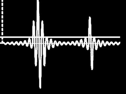
30 Size Comparison 200 V egan FET D-PAK 5.76 mm² Drawn To Scale 65.3 mm² 30 30
31 Key Applications Wireless Power Transmission GaN Enabled RF DC-DC Envelope Tracking GaN Enabled RadHard Power Over Ethernet RF Transmission Network and Server Power Supplies Point of Load Modules Energy Efficient Lighting Class D Audio 31 31
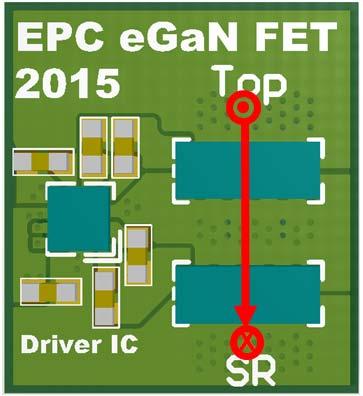
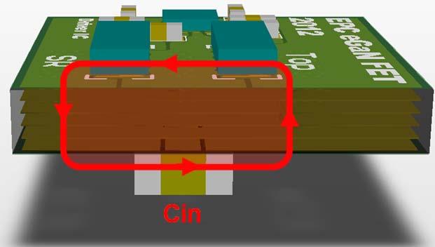
32 Design Basics Agenda Gate Driver Requirements Layout Thermal Management 32 32
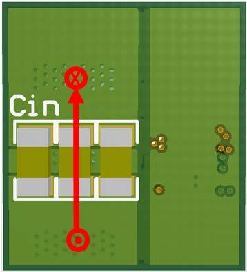
33 E-Mode Gate Drive - Low V GS(ON) Overhead V GS(Max) = 6 V 33 33
34 Gate Drive Solution No overshoot: R G 4 ( LG + L C GS S ) Minimize inductance Tight gate drive layout BGA and LGA minimizes package inductance Choose correct resistance Separate source and sink transistors allowing for separate drive paths
35 Bootstrap Supply +5V HB VIN LEVEL SHIFT HOH HOL Switch can be node negative during low side diode conduction Regulated high side supply Minimal dead time and slow bootstrap HS 35 35
36 High Side Regulation LM5113 Bootstrap clamp limits floating (HS) power supply Separate control inputs allow accurate, flexible tuning to minimize dead-time Well matched channel-to-channel propagation delays are critical Optional Schottky in parallel Texas Instruments, Gate Drivers for Enhancement Mode GaN Power FETs 100 V Half-Bridge and Low- Side Drivers Enable Greater Efficiency, Power Density, and Simplicity, SNVB
37 Layout 37 37

 2.5 2 1.5 1 0.")


 90 85")

 38")
38 Packaging Evolution So-8 LFPAK DirectFET LGA egan Power Loss (W) Device Loss Breakdown 82% 18% Package Die 73% 27% 47% 53% So-8 LFPAK DirectFET LGA V IN =12V V OUT =1.2V I OUT =20A F S =1MHz 18% 82% Efficiency (%) So-8 LFPAK DirectFET egan Switching Frequency (MHz) 38 38

39 Generating Kelvin Source Connection Source Return Source R Source C GD Substrate Gate R Series R G C GS R Sink Drain L S Minimize Common Source Inductance 39 39
40 Buck Converter Parasitics C in T SR L S : Common Source Inductance L Loop : High Frequency Power Loop Inductance Power Loss(W) Power Loss vs Parasitic Inductance Ls L Loop Parasitic Inductance (nh) V IN =12 V, V OUT =1.2 V, F S =1 MHz, I OUT = 20 A 40 40
 V IN =12 V, V OUT =1.2 V, F S =1 MHz, L=150 nh Experimental Prototype L LOOP 0.")
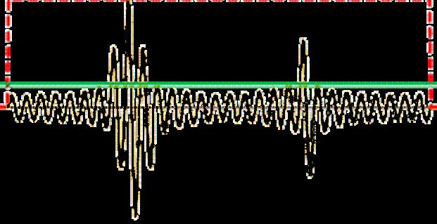
41 Layout Impact on Efficiency Efficiency (%) Measured Efficiency 40V MOSFET 3x3mm LFPAK L Loop 3nH L Loop 0.4nH L Loop 1.0nH L Loop 1.6nH L Loop 2.9nH Output Current (I OUT ) V IN =12 V, V OUT =1.2 V, F S =1 MHz, L=150 nh Experimental Prototype L LOOP 0.4 nh 41 41
42 Layout Impact on Peak Voltage L Loop 1.0 nh L Loop 0.4 nh 70% Overshoot 30% Overshoot Switching Node Voltage V IN =12 V V OUT =1.2 V I OUT =20 A F S =1 MHz L=150 nh 42 42


43 Conventional Lateral Layout Top View Side View 43 43
44 Conventional Vertical Layout Top View Side View Bottom View 44 44


45 Optimal Layout Top View Side View Top View Inner Layer
46 Power Loss Comparison Power Loss (W) Lateral Power Loop Optimal Power Loop Vertical Power Loop High Frequency Loop Inductance (L LOOP ) V IN =12 V V OUT =1.2 V I OUT =20 A F S =1 MHz L=300 nh T/SR: EPC2015 Driver LM
47 Efficiency Comparison Efficiency (%) V MOSFET Design 1 Optimal Design 1 Vertical Design 1 Lateral Design Output Current (I OUT ) V IN =12 V V OUT =1.2 V F S =1 MHz L=300 nh T/SR: EPC2015 Driver LM

48 egan FET vs. MOSFET Si MOSFET egan FET V IN =12 V V OUT =1.2 V I OUT =20 A F S =1 MHz L=300 nh egan FET T/SR: EPC2015 MOSFET T:BSZ097N04LS SR:BSZ040N04LS 48
49 Layout Summary egan FETs improve performance in high switching frequency converters CSI is a critical component for maximizing switching performance Gate drive loop inductance limits switching speed Optimizing power loop inductance improves efficiency and minimizes voltage overshoot Current measurements affect performance Voltage measurements are bandwidth limited Reduced ringing reduces EMI 49 49
50 Thermal Management 50 50
51 Thermal Management Heat Is Generated In GaN Material Essentially On The Surface Of The Die Silicon Substrate Active GaN Device Region Solder Bars Copper Traces Printed Circuit Board 51 51
52 Thermal Management Silicon Substrate R ƟJC Active GaN Device Region Solder Bars R ƟJB Copper Traces Printed Circuit Board Two Paths For Heat: Through The Back Of The Die Or Through The Solder Contacts Into The PCB 52 52

53 Thermal Resistance with Heat Sink Silicon Substrate Active GaN Device Region R ƟJC Solder Bars R ƟJB Copper Traces Printed Circuit Board 53 53
54 Thermal Resistance with Heat Sink 2 22 Printed Circuit Board 1 Thermal Interface Material on sides of die too 54 54
55 Thermal Model with Heat Sink Back of Die temperature Heatsink R θtim R θha R θtim Ambient Temperature Junction temperature R θjc R θjc R θjb R θjb Other PCB losses Device 1 Power dissipation R θspread R θpcba Ambient Temperature Device 2 Power dissipation 55 55


56 Thermal Results Possible to remove up to 5 W from small EPC die with double sided cooling 56
57 Design Example Agenda Hard Switched Circuits Buck Converter Isolated Full Bridge Envelope Tracking Resonant Circuits Intermediate Bus Converter 57 57
58 Buck Converters 58

59 High Frequency Buck Converters D. Reusch, D. Gilham, Y. Su, and F.C. Lee, C, Gallium Nitride Based 3D Integrated Non-Isolated Point of Load Module, APEC


60 EPC9107 Optimal Layout Buck Module Switching Node Voltage V IN =28 V I OUT =15 A EPC9107 Demonstration Board V IN =12-28 V V OUT =3.3 V I OUT =15 A F S =1 MHz 2 x EPC V/ div 60
61 EPC9107 Demonstration Board Efficiency (%) V IN 19 V IN 24 V IN 28 V IN Output Current (Io) V OUT =3.3 V F S =1 MHz GaN T/SR: EPC2015 Driver LM
62 Isolated Full Bridge 62
63 100 V Hard Switching FOM 160 FOM=(Q GD +Q GS2 )*R DSON (nc*ω) Q GS2 Q GS2 Q GS2 Q Q GS2 GD Q GD Q GS2 Q GD Q GD Q GD 100V egan FET 80V MOSFET 1 80V MOSFET 2 80V MOSFET 3 80V MOSFET 4 V DS =0.5*V DS, I DS = 15 A 63 63


64 Regulated Full Bridge Converter EPC9102 Demo board Full Bridge, Vin, 12 V, 200 W, 375 khz 64 64

65 Efficiency Comparison 375 khz egan FET 250 khz MOSFET Regulated 12 V Output 65 65
66 Brick Converter Summary Topologies varied Optimization as important as device selection Efficiency is key to power density Maximum power loss is fixed. Good comparison requires identical designs Given topology, egan FETs will outperform MOSFETs based on superior FOM 66 66
67 Overview of Envelope Tracking World of Radio Frequency Power Amplifiers (RFPA) is changing. Increased efficiency driven by: Improved battery life Reduced cooling Reduced size Lower cost of operation 67


68 Peak to Average Power Ratio Same average Normalized to same peak Ref: Nujira.com website 68


69 Effect of PAPR Average Power Peak Power Fixed supply PAPR = 0dB Peak efficiency up to 65% Average efficiency only 25 % Increasing PAPR Output Probability Output Power (dbm) 69
 Only 1/3 the losses Envelope Tracking Output Probability Average Power")
70 Effect of Envelope Tracking Average efficiency > 50 % (incl. ET) Only 1/3 the losses Envelope Tracking Output Probability Average Power Output Power (dbm) 70

71 RFPA Standards* Up to 20 MHz Carrier bandwidth required Required ET supply BW up to 5x higher if linear control *Ref: website 71
72 Envelope Tracking Supply ET power supply topologies vary Open loop boost full BW required Closed loop linear-assisted Buck* Buck ~ 10% Bandwidth ~ 90% Power Linear AMP ~ 10% Power Highest 90% of Bandwidth *V. Yousefzadeh, et. Al, Efficiency optimization in linear-assisted switching power converters for envelope tracking in RF power amplifiers, ISCAS
73 egan FET based Buck(s) for ET 1300 W DVB* 8 MHz BW and 8 db PAPR Linear-assisted Buck for ET 4 phase x 1 MHz Buck with up to 800 khz band width 45 V IN, 22 V OUT / 15 A OUT (Avg) Pure Buck option for ET (Push frequency) 10 phase x 4 MHz Buck with up to 8 MHz band width 45 V IN, 22 V OUT / 6 A OUT (Avg) *Representative of a high power ET buck in HV LDMOS, such as that implemented by ET specialist Nujira. 73


74 6 A OUT / 4 MHz Single φ Buck Modified an EPC9006 development board 45 V IN Before After Gappad GP mil 22 V OUT Common LM5113TE EPC
75 Efficiency Results 98% 10x potential bandwidth require 2.5x more phases and 2x losses 16 97% 14 96% 12 Efficiency (%) 95% 94% 93% 4 MHz Efficiency Power loss (W) 92% 1 MHz Efficiency 4 91% 90% 2 1 MHz Losses Output Power (W) 4 MHz Losses 75


76 Loss Breakdown EPC2001 EPC2007 EPC2001 EPC MHz EPC MHz EPC9006 Future die size optimization possible 76 76


77 Higher Frequency ET Results* EPC1014 BSC016N04LSG 24 V IN to 12 V OUT Buck 20 to 30 pp improvement! 4 MHz 7 MHz 10 MHz *D. Čučak, et. al, Application of egan FETs for highly efficient Radio Frequency Power Amplifier, CIPS
78 Envelope Tracking Summary egan FETs are an enabling technology for ET Low charge reduces delay and switching times Thermally possible - with double sided cooling Results are representative, but not optimized Improve inductor selection Improve thermal design Reduce high side peak device temp by reducing low side device size to reduce Q OSS losses Power and # of phases application specific 78 78
79 Resonant Converters 79
80 100 V Soft Switching FOM 350 FOM=(Q OSS or Q G )*R DSON (nc*ω) Q OSS Q OSS Q OSS Q G Q G Q G 100 V EPC V BSC057N08NS3G 80 V BSZ123N08NS3G V DS =48 V 80

81 egan FET vs. MOSFET 81
82 ZVS Switching Comparison T ZVS = 42 ns egan FET V DS MOSFET V DS T ZVS = 87 ns MOSFET V GS egan FET V GS F S = 1.2 MHz, V IN = 48 V, and V OUT = 12 V 82


83 Duty Cycle Comparison D egan FET = 42% D MOSFET = 34% MOSFET V GS egan FET V DS egan FET V GS MOSFET V DS F S = 1.2 MHz, V IN = 48 V, and V OUT = 12 V 83
84 Efficiency Comparison Efficiency (%) MHz egan FET 1.2 MHz MOSFET 10 W 12 W 14 W Power Loss (W) MHz MOSFET 1.2 MHz egan FET Output Current (I OUT ) Output Current (I OUT ) F S = 1.2 MHz, V IN = 48 V, and V OUT = 12 V 84


85 Loss Breakdown Power Loss (W) Gate Drive Transfomrer Core Conduction + Turn Off 2 0 egan FET I OUT = 2.5 A MOSFET I OUT = 2.5 A egan FET I OUT = 20 A MOSFET I OUT = 20 A F S = 1.2 MHz, V IN = 48 V, and V OUT = 12 V 85


86 EPC9105 Bus Converter EPC9105 Demonstration Board V IN, 12 V OUT, 350 W, 1.2 MHz L IN L K1 2 SR V IN+ C IN Q 1 Q 3 4:1 * * * Q 6, Q 7 V OUT+ L OUT C RES C OUT V IN- Q 2 Q 4 L K2 2 SR Q 5, Q 8 V OUT- 86
87 Resonant Converter Summary egan FETs improve high frequency resonant converter performance Lower output charge Lower gate charge More power delivery per cycle 87 87
88 Summary GaN transistors have the potential to replace silicon power MOSFETs in power conversion applications with a low-cost and higher efficiency solution egan FETs are straightforward to use, but care must be taken due to the higher switching speeds compared with power MOSFETs GaN transistors enable exciting new applications such as RF Envelope Tracking 88 88
GaN is Crushing Silicon. EPC - The Leader in GaN Technology IEEE PELS
 GaN is Crushing Silicon EPC - The Leader in GaN Technology IEEE PELS 2014 www.epc-co.com 1 Agenda How egan FETs work Hard Switched DC-DC converters High Efficiency point-of-load converter Envelope Tracking
The egan FET Journey Continues
 The egan FET Journey Continues Understanding the Effect of PCB Layout on Circuit Performance in a High Frequency Gallium Nitride Based Point of Load Converter David Reusch and Johan Strydom Efficient Power
GaN on Silicon Technology: Devices and Applications
 The egan FET Journey Continues GaN on Silicon Technology: Devices and Applications Alex Lidow Efficient Power Conversion Corporation EPC - The Leader in egan FETs May, 2013 PCIM 2013 www.epc-co.com 1 Agenda
GaN Transistors for Efficient Power Conversion
 GaN Transistors for Efficient Power Conversion Alex Lidow and David Reusch Efficient Power Conversion www.epc-co.com 1 Agenda How GaN works and the state-of-theart Design Basics Design Examples What is
GaN Brings About a New Way of Thinking to Power Conversion Stephen Colino Efficient Power Conversion Corporation
 GaN Brings About a New Way of Thinking to Power Conversion Stephen Colino Efficient Power Conversion Corporation 1 GaN Wide Bandgap Hetero Junction Distance electrons need to travel Si Conductivity GaN
Improving Performance of High Speed GaN Transistors Operating in Parallel for High Current Applications
 Improving Performance of High Speed GaN Transistors Operating in Parallel for High Current Applications David Reusch and Johan Strydom Efficient Power Conversion Corporation (EPC), El Segundo, CA, USA.
GS61004B 100V enhancement mode GaN transistor Preliminary Datasheet
 Features 100V enhancement mode power switch Bottom-side cooled configuration R DS(on) = 15 mω I DS(max) = 45 A Ultra-low FOM Island Technology die Low inductance GaNPX package Easy gate drive requirements
Introducing egan IC targeting Highly Resonant Wireless Power
 Dr. M. A. de Rooij The egan FET Journey Continues Introducing egan IC targeting Highly Resonant Wireless Power Efficient Power Conversion Corporation EPC - The Leader in egan FETs www.epc-co.com 1 Agenda
Fig. 1 - Enhancement mode GaN has a circuiut schematic similar to silicon MOSFETs with Gate (G), Drain (D), and Source (S).
, Drain (D), and Source (S).") GaN Basics: FAQs Sam Davis; Power Electronics Wed, 2013-10-02 Gallium nitride transistors have emerged as a high-performance alternative to silicon-based transistors, thanks to the technology's ability
GaN Basics: FAQs Sam Davis; Power Electronics Wed, 2013-10-02 Gallium nitride transistors have emerged as a high-performance alternative to silicon-based transistors, thanks to the technology's ability
GS61008T Top-side cooled 100 V E-mode GaN transistor Preliminary Datasheet
 Features 100 V enhancement mode power switch Top-side cooled configuration R DS(on) = 7 mω I DS(max) = 90 A Ultra-low FOM Island Technology die Low inductance GaNPX package Easy gate drive requirements
GS61008T Top-side cooled 100 V E-mode GaN transistor Preliminary Datasheet
 Features 100 V enhancement mode power switch Top-side cooled configuration R DS(on) = 7 mω I DS(max) = 90 A Ultra-low FOM Island Technology die Low inductance GaNPX package Easy gate drive requirements
Performance Comparison for A4WP Class-3 Wireless Power Compliance between egan FET and MOSFET in a ZVS Class D Amplifier
 The egan FET Journey Continues Performance Comparison for A4WP Class-3 Wireless Power Compliance between egan FET and MOSFET in a ZVS Class D Amplifier EPC - The leader in GaN Technology www.epc-co.com
Unlocking the Power of GaN PSMA Semiconductor Committee Industry Session
 Unlocking the Power of GaN PSMA Semiconductor Committee Industry Session March 24 th 2016 Dan Kinzer, COO/CTO dan.kinzer@navitassemi.com 1 Mobility (cm 2 /Vs) EBR Field (MV/cm) GaN vs. Si WBG GaN material
GS61008P Bottom-side cooled 100 V E-mode GaN transistor Preliminary Datasheet
 Features 100 V enhancement mode power switch Bottom-side cooled configuration R DS(on) = 7 mω I DS(max) = 90 A Ultra-low FOM Island Technology die Low inductance GaNPX package Easy gate drive requirements
GS66516T Top-side cooled 650 V E-mode GaN transistor Preliminary Datasheet
 Features 650 V enhancement mode power switch Top-side cooled configuration R DS(on) = 25 mω I DS(max) = 60 A Ultra-low FOM Island Technology die Low inductance GaNPX package Easy gate drive requirements
GS P Bottom-side cooled 100 V E-mode GaN transistor Preliminary Datasheet. Features. Applications. Description.
 Features 100 V enhancement mode power switch Bottom-side cooled configuration R DS(on) = 5 mω I DS(max) = 120 A Ultra-low FOM Island Technology die Low inductance GaNPX package Easy gate drive requirements
GaAs PowerStages for Very High Frequency Power Supplies. Greg Miller Sr. VP - Engineering Sarda Technologies
 GaAs PowerStages for Very High Frequency Power Supplies Greg Miller Sr. VP - Engineering Sarda Technologies gmiller@sardatech.com Agenda Case for Higher Power Density Voltage Regulators Limitations of
Breaking Speed Limits with GaN Power ICs March 21 st 2016 Dan Kinzer, COO/CTO
 Breaking Speed Limits with GaN Power ICs March 21 st 2016 Dan Kinzer, COO/CTO dan.kinzer@navitassemi.com 1 Efficiency The Need for Speed Tomorrow? Today 100kHz 1MHz 10MHz Bulky, Heavy Small, Light & Expensive
100V ENHANCEMENT MODE HIGH ELECTRON MOBILITY TRANSISTOR (HEMT) Michele Rossitto. Marketing Director MOSFETs and Power ICs
 Michele Rossitto. Marketing Director MOSFETs and Power ICs") 100V ENHANCEMENT MODE HIGH ELECTRON MOBILITY TRANSISTOR (HEMT) Michele Rossitto Marketing Director MOSFETs and Power ICs 100V GaN in PowerPAK 6 x 5 mm² Package Enhancement Mode GaN Transistor Superior
100V ENHANCEMENT MODE HIGH ELECTRON MOBILITY TRANSISTOR (HEMT) Michele Rossitto Marketing Director MOSFETs and Power ICs 100V GaN in PowerPAK 6 x 5 mm² Package Enhancement Mode GaN Transistor Superior
GS61008P Bottom-side cooled 100 V E-mode GaN transistor Preliminary Datasheet. Features. Applications. Description. Circuit Symbol.
 Features 100 V enhancement mode power switch Bottom-side cooled configuration R DS(on) = 7 mω I DS(max) = 90 A Ultra-low FOM Island Technology die Low inductance GaNPX package Easy gate drive requirements
GS66508T Top-side cooled 650 V E-mode GaN transistor Preliminary Datasheet
 Features 650 V enhancement mode power switch Top-side cooled configuration R DS(on) = 50 mω I DS(max) = 30 A Ultra-low FOM Island Technology die Low inductance GaNPX package Easy gate drive requirements
GS66506T Top-side cooled 650 V E-mode GaN transistor Preliminary Datasheet
 Features 650 V enhancement mode power switch Top-side cooled configuration R DS(on) = 67 mω I DS(max) = 22.5 A Ultra-low FOM Island Technology die Low inductance GaNPX package Easy gate drive requirements
GS61004B 100V enhancement mode GaN transistor Preliminary Datasheet
 Features 100V enhancement mode power switch Bottom-side cooled configuration R DS(on) = 15 mω I DS(max) = 45 A Ultra-low FOM Island Technology die Low inductance GaNPX package Easy gate drive requirements
Symbol Parameter Typical
 PRODUCT SUMMARY (TYPICAL) V DS (V) 600 R DS(on) ( ) 0.29 Q rr (nc) 29 Features Low Q rr Free-wheeling diode not required Low-side Quiet Tab for reduced EMI RoHS compliant High frequency operation Applications
235 W Maximum Power Dissipation (whole module) 470 T J Junction Operating Temperature -40 to 150. Torque strength
 470 T J Junction Operating Temperature -40 to 150. Torque strength") Discontinued PRODUCT SUMMARY (TYPICAL) V DS (V) 600 R DS(on) (m ) 30 GaN Power Hybrid HEMT Half-Bridge Module Features High frequency operation Free-wheeling diode not required Applications Compact DC-DC
Discontinued PRODUCT SUMMARY (TYPICAL) V DS (V) 600 R DS(on) (m ) 30 GaN Power Hybrid HEMT Half-Bridge Module Features High frequency operation Free-wheeling diode not required Applications Compact DC-DC
EPC8004 Enhancement Mode Power Transistor
 Enhancement Mode Power Transistor, V R DS(on), mω, A G D S EFFICIENT POWER CONVERSION HAL Gallium Nitride is grown on Silicon Wafers and processed using standard CMOS equipment leveraging the infrastructure
GS66508T Top-side cooled 650 V E-mode GaN transistor Preliminary Datasheet
 Features 650 V enhancement mode power switch Top-side cooled configuration R DS(on) = 50 mω I DS(max) = 30 A Ultra-low FOM Island Technology die Low inductance GaNPX package Easy gate drive requirements
GS66508T Top-side cooled 650 V E-mode GaN transistor Preliminary Datasheet
 Features 650 V enhancement mode power switch Top-side cooled configuration R DS(on) = 50 mω I DS(max) = 30 A Ultra-low FOM Island Technology die Low inductance GaNPX package Easy gate drive requirements
GS66516B Bottom-side cooled 650 V E-mode GaN transistor Preliminary Datasheet
 Features 650 V enhancement mode power switch Bottom-side cooled configuration R DS(on) = 25 mω I DS(max) = 60 A Ultra-low FOM Island Technology die Low inductance GaNPX package Easy gate drive requirements
GS66516B Bottom-side cooled 650 V E-mode GaN transistor Preliminary Datasheet
 Features 650 V enhancement mode power switch Bottom-side cooled configuration R DS(on) = 25 mω I DS(max) = 60 A Ultra-low FOM Island Technology die Low inductance GaNPX package Easy gate drive requirements
GaN in Practical Applications
 in Practical Applications 1 CCM Totem Pole PFC 2 PFC: applications and topology Typical AC/DC PSU 85-265 V AC 400V DC for industrial, medical, PFC LLC 12, 24, 48V DC telecomm and server applications. PFC
GS66502B Bottom-side cooled 650 V E-mode GaN transistor Preliminary Datasheet
 GS66502B Features 650 V enhancement mode power switch Bottom-side cooled configuration R DS(on) = 200 mω I DS(max) = 7.5 A Ultra-low FOM Island Technology die Low inductance GaNPX package Easy gate drive
EPC2015 Enhancement Mode Power Transistor
 EPC5 EPC5 Enhancement Mode Power Transistor V DSS, 4 V R DS(ON), 4 mw I D, A PRELIMINARY EFFICIENT POWER CONVERSION HAL Gallium Nitride is grown on Silicon Wafers and processed using standard CMOS equipment
Designing reliable and high density power solutions with GaN. Created by: Masoud Beheshti Presented by: Paul L Brohlin
 Designing reliable and high density power solutions with GaN Created by: Masoud Beheshti Presented by: Paul L Brohlin What will I get out of this presentation? Why GaN? Integration for System Performance
Symbol Parameter Typical
 PRODUCT SUMMARY (TYPICAL) V DS (V) 650 R DS(on) (m ) 110 Q rr (nc) 54 Features Low Q rr Free-wheeling diode not required Low-side Quiet Tab for reduced EMI RoHS compliant High frequency operation Applications
TPH3202PS TPH3202PS. GaN Power Low-loss Switch PRODUCT SUMMARY (TYPICAL) TO-220 Package. Absolute Maximum Ratings (T C =25 C unless otherwise stated)
 TO-220 Package. Absolute Maximum Ratings (T C =25 C unless otherwise stated)") PRODUCT SUMMARY (TYPICAL) V DS (V) 600 R DS(on) ( ) 0.29 Q rr (nc) 29 Features Low Q rr Free-wheeling diode not required Low-side Quiet Tab for reduced EMI GSD pin layout improves high speed design RoHS
PRODUCT SUMMARY (TYPICAL) V DS (V) 600 R DS(on) ( ) 0.29 Q rr (nc) 29 Features Low Q rr Free-wheeling diode not required Low-side Quiet Tab for reduced EMI GSD pin layout improves high speed design RoHS
GS66504B Bottom-side cooled 650 V E-mode GaN transistor Preliminary Datasheet
 Features 650 V enhancement mode power switch Bottom-side cooled configuration R DS(on) = 100 mω I DS(max) = 15 A Ultra-low FOM Island Technology die Low inductance GaNPX package Easy gate drive requirements
Michael de Rooij Efficient Power Conversion Corporation
 The egan FET Journey Continues Performance comparison using egan FETs in 6.78 MHz class E and ZVS class D Wireless Power Transfer Michael de Rooij Efficient Power Conversion Corporation EPC - The Leader
GS66508P Bottom-side cooled 650 V E-mode GaN transistor Preliminary Datasheet
 Features 650 V enhancement mode power switch Bottom-side cooled configuration R DS(on) = 50 mω I DS(max) = 30 A Ultra-low FOM Island Technology die Low inductance GaNPX package Easy gate drive requirements
EPC2007C Enhancement Mode Power Transistor
 EPC7C EPC7C Enhancement Mode Power Transistor V DSS, V R DS(on), 3 mw I D, 6 A NEW PRODUCT EFFICIENT POWER CONVERSION HAL Gallium Nitride is grown on Silicon Wafers and processed using standard CMOS equipment
EPC2014 Enhancement Mode Power Transistor
 EPC4 EPC4 Enhancement Mode Power Transistor V DSS, V R DS(ON), 6 mw I D, A NEW PRODUCT EFFICIENT POWER CONVERSION HAL Gallium Nitride is grown on Silicon Wafers and processed using standard CMOS equipment
TPH3207WS TPH3207WS. GaN Power Low-loss Switch PRODUCT SUMMARY (TYPICAL) Absolute Maximum Ratings (T C =25 C unless otherwise stated)
 Absolute Maximum Ratings (T C =25 C unless otherwise stated)") PRODUCT SUMMARY (TYPICAL) V DS (V) 650 R DS(on) (m ) 35 Q rr (nc) 175 Features Low Q rr Free-wheeling diode not required Quiet Tab for reduced EMI at high dv/dt GSD pin layout improves high speed design
PRODUCT SUMMARY (TYPICAL) V DS (V) 650 R DS(on) (m ) 35 Q rr (nc) 175 Features Low Q rr Free-wheeling diode not required Quiet Tab for reduced EMI at high dv/dt GSD pin layout improves high speed design
Second Generation egan FETs are Lead Free and Offer Improved Performance Alex Lidow, CEO, Efficient Power Conversion Corporation
 Second Generation egan FETs are Lead Free and Offer Improved Performance Alex Lidow, CEO, Efficient Power Conversion Corporation EFFICIENT POWER CONVERSION Since March, 11 Efficient Power Conversion Corporation
Designing High density Power Solutions with GaN Created by: Masoud Beheshti Presented by: Xaver Arbinger
 Designing High density Power Solutions with GaN Created by: Masoud Beheshti Presented by: Xaver Arbinger Topics Why GaN? Integration for Higher System Performance Application Examples Taking GaN beyond
Wide Band-Gap (SiC and GaN) Devices Characteristics and Applications. Richard McMahon University of Cambridge
 Devices Characteristics and Applications. Richard McMahon University of Cambridge") Wide Band-Gap (SiC and GaN) Devices Characteristics and Applications Richard McMahon University of Cambridge Wide band-gap power devices SiC : MOSFET JFET Schottky Diodes Unipolar BJT? Bipolar GaN : FET
Wide Band-Gap (SiC and GaN) Devices Characteristics and Applications Richard McMahon University of Cambridge Wide band-gap power devices SiC : MOSFET JFET Schottky Diodes Unipolar BJT? Bipolar GaN : FET
GS66508B Bottom-side cooled 650 V E-mode GaN transistor Preliminary Datasheet
 Features 650 V enhancement mode power switch Bottom-side cooled configuration R DS(on) = 50 mω I DS(max) = 30 A Ultra-low FOM Island Technology die Low inductance GaNPX package Easy gate drive requirements
Appendix: Power Loss Calculation
 Appendix: Power Loss Calculation Current flow paths in a synchronous buck converter during on and off phases are illustrated in Fig. 1. It has to be noticed that following parameters are interrelated:
Designing a 99% Efficient Totem Pole PFC with GaN. Serkan Dusmez, Systems and applications engineer
 Designing a 99% Efficient Totem Pole PFC with GaN Serkan Dusmez, Systems and applications engineer 1 What will I get out of this session? Purpose: Why GaN Based Totem-pole PFC? Design guidelines for getting
Power of GaN. Enabling designers to create smaller, more efficient and higher-performing AC/DC power supplies
 Power of GaN Enabling designers to create smaller, more efficient and higher-performing AC/DC power supplies Steve Tom Product Line Manager, GaN Products stom@ti.com Solving power and energy-management
EPC2107 Enhancement-Mode GaN Power Transistor Half-Bridge with Integrated Synchronous Bootstrap
 EPC7 Enhancement-Mode GaN Power Transistor Half-Bridge with Integrated Synchronous Bootstrap V DSS, V R DS(on), 9 m I D,.7 A EFFICIENT POWER CONVERSION HAL EPC7 Gallium Nitride is grown on Silicon Wafers
Designing Reliable and High-Density Power Solutions with GaN
 Designing Reliable and High-Density Power Solutions with GaN 1 Detailed agenda Why is GaN Exciting GaN Fundamentals Cost and Reliability Totem Pole PFC Isolated LLC Motor Drive LiDAR Driving GaN Choosing
High Current Voltage Regulator Module (VRM) Uses DirectFET MOSFETs to Achieve Current Densities of 25A/in2 at 1MHz to Power 32-bit Servers
 Uses DirectFET MOSFETs to Achieve Current Densities of 25A/in2 at 1MHz to Power 32-bit Servers") High Current Voltage Regulator Module (VRM) Uses DirectFET MOSFETs to Achieve Current Densities of 25A/in2 at 1MHz to Power 32-bit Servers Ralph Monteiro, Carl Blake and Andrew Sawle, Arthur Woodworth
High Current Voltage Regulator Module (VRM) Uses DirectFET MOSFETs to Achieve Current Densities of 25A/in2 at 1MHz to Power 32-bit Servers Ralph Monteiro, Carl Blake and Andrew Sawle, Arthur Woodworth
IR3101 Series 1.6A, 500V
 Half-Bridge FredFet and Integrated Driver Features Output power FredFets in half-bridge configuration High side gate drive designed for bootstrap operation Bootstrap diode integrated into package. Lower
EPC2016C Enhancement Mode Power Transistor
 EPC6C EPC6C Enhancement Mode Power Transistor V DSS, V R DS(on), 6 mω I D, 8 A G D S EFFICIENT POWER CONVERSION HAL Gallium Nitride s exceptionally high electron mobility and low temperature coefficient
HCS65R110FE (Fast Recovery Diode Type) 650V N-Channel Super Junction MOSFET
 650V N-Channel Super Junction MOSFET") HCS65R110FE (Fast Recovery Diode Type) 650V N-Channel Super Junction MOSFET Features Very Low FOM (R DS(on) X Q g ) Extremely low switching loss Excellent stability and uniformity 100% Avalanche Tested
HCS65R110FE (Fast Recovery Diode Type) 650V N-Channel Super Junction MOSFET Features Very Low FOM (R DS(on) X Q g ) Extremely low switching loss Excellent stability and uniformity 100% Avalanche Tested
Advantages of Using Gallium Nitride FETs in Satellite Applications
 White Paper Advantages of Using Gallium Nitride FETs in Satellite Applications Kiran Bernard, Applications Engineer, Industrial Analog & Power Group, Renesas Electronics Corp. February, 2018 Abstract Silicon
ELEC-E8421 Components of Power Electronics
 ELEC-E8421 Components of Power Electronics MOSFET 2015-10-04 Metal-Oxide-Semiconductor Field-Effect-Transistor (MOSFET) Vertical structure makes paralleling of many small MOSFETs on the chip easy. Very
T C =25 unless otherwise specified. Symbol Parameter Value Units V DSS Drain-Source Voltage 40 V
 40V N-Channel Trench MOSFET June 205 BS = 40 V R DS(on) typ = 3.3mΩ = 30 A FEATURES Originative New Design Superior Avalanche Rugged Technology Excellent Switching Characteristics Unrivalled Gate Charge
High Performance ZVS Buck Regulator Removes Barriers To Increased Power Throughput In Wide Input Range Point-Of-Load Applications
 WHITE PAPER High Performance ZVS Buck Regulator Removes Barriers To Increased Power Throughput In Wide Input Range Point-Of-Load Applications Written by: C. R. Swartz Principal Engineer, Picor Semiconductor
HCI70R500E 700V N-Channel Super Junction MOSFET
 HCI70R500E 700V N-Channel Super Junction MOSFET Features Very Low FOM (R DS(on) X Q g ) Extremely low switching loss Excellent stability and uniformity 100% Avalanche Tested Higher dv/dt ruggedness Application
IRFI4212H-117P. Description. Key Parameters g V DS 100 V R DS(ON) 10V 58 m: Q g typ. 12 nc Q sw typ. 6.9 nc R G(int) typ. 3.
 10V 58 m: Q g typ. 12 nc Q sw typ. 6.9 nc R G(int) typ. 3.") DIGITAL AUDIO MOSFET PD - 97249A IRFI422H-7P Features Ÿ Integrated half-bridge package Ÿ Reduces the part count by half Ÿ Facilitates better PCB layout Ÿ Key parameters optimized for Class-D audio amplifier
DIGITAL AUDIO MOSFET PD - 97249A IRFI422H-7P Features Ÿ Integrated half-bridge package Ÿ Reduces the part count by half Ÿ Facilitates better PCB layout Ÿ Key parameters optimized for Class-D audio amplifier
Driving egan TM Transistors for Maximum Performance
 Driving egan TM Transistors for Maximum Performance Johan Strydom: Director of Applications, Efficient Power Conversion Corporation Alex Lidow: CEO, Efficient Power Conversion Corporation The recent introduction
High voltage GaN cascode switches shift power supply design trends. Eric Persson Executive Director, GaN Applications and Marketing
 High voltage GaN cascode switches shift power supply design trends Eric Persson Executive Director, GaN Applications and Marketing September 4, 2014 1 Outline for Today s PSMA PTR Presentation Why do we
The Quest for High Power Density
 The Quest for High Power Density Welcome to the GaN Era Power Conversion Technology Drivers Key design objectives across all applications: High power density High efficiency High reliability Low cost 2
Driving egan FETs in High Performance Power Conversion Systems
 in High Performance Power Conversion Systems EFFICIENT POWER CONVERSION Alexander Lidow, Johan Strydom, and Michael de Rooij, Efficient Power Conversion Corporation Andrew Ferencz, Consultant for Efficient
HCD80R1K4E 800V N-Channel Super Junction MOSFET
 HCD80R1K4E 800V N-Channel Super Junction MOSFET Features Very Low FOM (R DS(on) X Q g ) Extremely low switching loss Excellent stability and uniformity 100% Avalanche Tested Application Switch Mode Power
Get Your GaN PhD in Less Than 60 Minutes!
 Get Your GaN PhD in Less Than 60 Minutes! 1 Detailed agenda Why is GaN Exciting GaN Fundamentals Cost and Reliability Totem Pole PFC Isolated LLC Motor Drive LiDAR Driving GaN Choosing a GaN Tools 4 Why
Class D Audio Amplifier Design
 Class D Audio Amplifier Design Class D Amplifier Introduction Theory of Class D operation, topology comparison Gate Driver How to drive the gate, key parameters in gate drive stage MOSFET How to choose,
GaN Power ICs at 1 MHz+: Topologies, Technologies and Performance
 GaN Power ICs at 1 MHz+: Topologies, Technologies and Performance PSMA Industry Session, Semiconductors Dan Kinzer, CTO/COO dan.kinzer@navitassemi.com March 2017 Power Electronics: Speed & Efficiency are
IRF6641TRPbF DIGITAL AUDIO MOSFET. Key Parameters V DS 200 V R DS(ON) V GS = 10V 51 m Qg typ. 34 nc R G(int) typ. 1.0
 V GS = 10V 51 m Qg typ. 34 nc R G(int) typ. 1.0") Features Latest MOSFET silicon technology Key parameters optimized for Class-D audio amplifier applications Low R DS(on) for improved efficiency Low Qg for better THD and improved efficiency Low Qrr for
Features Latest MOSFET silicon technology Key parameters optimized for Class-D audio amplifier applications Low R DS(on) for improved efficiency Low Qg for better THD and improved efficiency Low Qrr for
HCD80R600R 800V N-Channel Super Junction MOSFET
 HCD80R600R 800V N-Channel Super Junction MOSFET Features Very Low FOM (R DS(on) X Q g ) Extremely low switching loss Excellent stability and uniformity 00% Avalanche Tested Application Switch Mode Power
Evaluation and Applications of 600V/650V Enhancement-Mode GaN Devices
 Evaluation and Applications of 600V/650V Enhancement-Mode GaN Devices Xiucheng Huang, Tao Liu, Bin Li, Fred C. Lee, and Qiang Li Center for Power Electronics Systems, Virginia Tech Blacksburg, VA, USA
DFP50N06. N-Channel MOSFET
 N-Channel MOSFET Features R DS(on) (Max.22 )@ =1V Gate Charge (Typical 36nC) Improved dv/dt Capability High ruggedness 1% Avalanche Tested 1.Gate 2.Drain 3.Source BS = 6V R DS(ON) =.22 ohm = 5A General
PWRLITE LD1010D High Performance N-Ch Vertical Power JFET Transistor with Schottky G D S
 www.lovoltech.com PWRLITE LD11D High Performance N-Ch Vertical Power JFET Transistor with Schottky Features Trench Power JFET with low threshold voltage Vth. Device fully ON with Vgs =.7V Optimum for Low
SiC Transistor Basics: FAQs
 SiC Transistor Basics: FAQs Silicon Carbide (SiC) MOSFETs exhibit higher blocking voltage, lower on state resistance and higher thermal conductivity than their silicon counterparts. Oct. 9, 2013 Sam Davis
egan FET Wireless Energy Transfer Solutions Efficient Power Conversion Corporation
 The egan FET Journey Continues egan FET Wireless Energy Transfer Solutions Efficient Power Conversion Corporation www.epc-co.com 1 Agenda Wireless Power Topologies Overview Wireless Power Results for each
I2-PAK G D S. T C = 25 C unless otherwise noted. Drain-Source Voltage 260 V. Symbol Parameter SLB40N26C/SLI40N26C Units R θjc
 SLB40N26C / SLI40N26C 260V N-Channel MOSFET General Description This Power MOSFET is produced using Maple semi s advanced planar stripe DMOS technology. This advanced technology has been especially tailored
Utilizing GaN transistors in 48V communications DC-DC converter design
 Utilizing GaN transistors in 48V communications DC-DC converter design Di Chen, Applications Engineering Manager and Jason Xu, Applications Engineer, GaN Systems - November 25, 2016 As the world s demand
High Power Fully Regulated Eighth-brick DC-DC Converter with GaN FETs
 High Power Fully Regulated Eighth-brick DC-DC Converter with GaN FETs John Glaser, Johan Strydom, and David Reusch Efficient Power Conversion Corporation 909 N. Sepulveda Blvd., Ste. 230 El Segundo, CA
Pitch Pack Microsemi full SiC Power Modules
 Pitch Pack Microsemi full SiC Power Modules October 2014 SiC Main Characteristics vs. Si Characteristics SiC vs. Si Results Benefits Breakdown field (MV/cm) Electron sat. velocity (cm/s) Bandgap energy
SLD8N6 65S / SLU8N65 5S
 SLD8N65S / SLU8N65S 650V N-Channel MOSFET General Description This Power MOSFET is produced using Maple semi s advanced planar stripe DMOS technology. This advanced technology has been especially tailored
TO-220 G. T C = 25 C unless otherwise noted. Drain-Source Voltage 80 V. Symbol Parameter MSP120N08G Units R θjc
 MSP120N08G 80V N-Channel MOSFET General Description Features This Power MOSFET is produced using Maple semi s advanced technology. which provides high performance in on-state resistance, fast switching
Features MIC2193BM. Si9803 ( 2) 6.3V ( 2) VDD OUTP COMP OUTN. Si9804 ( 2) Adjustable Output Synchronous Buck Converter
 6.3V ( 2) VDD OUTP COMP OUTN. Si9804 ( 2) Adjustable Output Synchronous Buck Converter") MIC2193 4kHz SO-8 Synchronous Buck Control IC General Description s MIC2193 is a high efficiency, PWM synchronous buck control IC housed in the SO-8 package. Its 2.9V to 14V input voltage range allows
MIC2193 4kHz SO-8 Synchronous Buck Control IC General Description s MIC2193 is a high efficiency, PWM synchronous buck control IC housed in the SO-8 package. Its 2.9V to 14V input voltage range allows
HCA80R250T 800V N-Channel Super Junction MOSFET
 HCA80R250T 800V N-Channel Super Junction MOSFET Features Very Low FOM (R DS(on) X Q g ) Extremely low switching loss Excellent stability and uniformity 100% Avalanche Tested Application Switch Mode Power
HCS80R1K4E 800V N-Channel Super Junction MOSFET
 HCS80R1K4E 800V N-Channel Super Junction MOSFET Features Very Low FOM (R DS(on) X Q g ) Extremely low switching loss Excellent stability and uniformity 100% Avalanche Tested Application Switch Mode Power
IRF6602/IRF6602TR1 HEXFET Power MOSFET
 l Application Specific MOSFETs l Ideal for CPU Core DC-DC Converters l Low Conduction Losses l Low Switching Losses l Low Profile (
HCD80R650E 800V N-Channel Super Junction MOSFET
 HCD80R650E 800V N-Channel Super Junction MOSFET Features Very Low FOM (R DS(on) X Q g ) Extremely low switching loss Excellent stability and uniformity 100% Avalanche Tested Application Switch Mode Power
Latest fast diode technology tailored to soft switching applications
 AN_201708_PL52_024 600 V CoolMOS CFD7 About this document Scope and purpose The new 600 V CoolMOS TM CFD7 is Infineon s latest high voltage (HV) SJ MOSFET technology with integrated fast body diode. It
IRF6646 DirectFET Power MOSFET
 Typical R DS(on) (Ω) V GS, Gate-to-Source Voltage (V) l RoHS compliant containing no lead or bromide l Low Profile (
Unleash SiC MOSFETs Extract the Best Performance
 Unleash SiC MOSFETs Extract the Best Performance Xuning Zhang, Gin Sheh, Levi Gant and Sujit Banerjee Monolith Semiconductor Inc. 1 Outline SiC devices performance advantages Accurate test & measurement
HRLD150N10K / HRLU150N10K 100V N-Channel Trench MOSFET
 HRLD15N1K / HRLU15N1K 1V N-Channel Trench MOSFET FEATURES Originative New Design Superior Avalanche Rugged Technology Excellent Switching Characteristics Unrivalled Gate Charge : 8 nc (Typ.) Extended Safe
GaN Power ICs: Integration Drives Performance
 GaN Power ICs: Integration Drives Performance Stephen Oliver, VP Sales & Marketing stephen.oliver@navitassemi.com Bodo s Power Conference, Munich December 5 th, 2017 Navitas Semiconductor Inc. World s
AN Analog Power USA Applications Department
 Using MOSFETs for Synchronous Rectification The use of MOSFETs to replace diodes to reduce the voltage drop and hence increase efficiency in DC DC conversion circuits is a concept that is widely used due
ThinPAK 8x8. New High Voltage SMD-Package. April 2010 Version 1.0
 ThinPAK 8x8 New High Voltage SMD-Package Version 1.0 Content Introduction Package Specification Thermal Concept Application Test Conditions Impact on Efficiency and EMI Switching behaviour Portfolio and
HCS70R350E 700V N-Channel Super Junction MOSFET
 HCS70R350E 700V N-Channel Super Junction MOSFET Features Very Low FOM (R DS(on) X Q g ) Extremely low switching loss Excellent stability and uniformity 100% Avalanche Tested Higher dv/dt ruggedness Application
HCS80R380R 800V N-Channel Super Junction MOSFET
 HCS8R38R 8V N-Channel Super Junction MOSFET Features Very Low FOM (R DS(on) X Q g ) Extremely low switching loss Excellent stability and uniformity % Avalanche Tested Application Switch Mode Power Supply
HCA60R080FT (Fast Recovery Diode Type) 600V N-Channel Super Junction MOSFET
 600V N-Channel Super Junction MOSFET") HCA60R080FT (Fast Recovery Diode Type) 600V N-Channel Super Junction MOSFET Features Very Low FOM (R DS(on) X Q g ) Extremely low switching loss Excellent stability and uniformity 00% Avalanche Tested
HCA60R080FT (Fast Recovery Diode Type) 600V N-Channel Super Junction MOSFET Features Very Low FOM (R DS(on) X Q g ) Extremely low switching loss Excellent stability and uniformity 00% Avalanche Tested
VDSS (V) 650 V(TR)DSS (V) 800. RDS(on)eff (mω) max* 85. QRR (nc) typ 90. QG (nc) typ 10
 650 V(TR)DSS (V) 800. RDS(on)eff (mω) max* 85. QRR (nc) typ 90. QG (nc) typ 10") TP65H070L Series 650V GaN FET PQFN Series Preliminary Description The TP65H070L 650V, 72mΩ Gallium Nitride (GaN) FET are normally-off devices. It combines state-of-the-art high voltage GaN HEMT and low
TP65H070L Series 650V GaN FET PQFN Series Preliminary Description The TP65H070L 650V, 72mΩ Gallium Nitride (GaN) FET are normally-off devices. It combines state-of-the-art high voltage GaN HEMT and low
I2-PAK G D S. T C = 25 C unless otherwise noted. Drain-Source Voltage 650 V. Symbol Parameter SLB10N65S SLI10N65S Units R θjc
 SLB10N65S/ SLI10N65S 650V N-Channel MOSFET General Description This Power MOSFET is produced using Maple semi s advanced planar stripe DMOS technology. This advanced technology has been especially tailored