60 W Adapter Documentation Package Evaluation Board User's Manual
|
|
|
- Wilfrid Potter
- 6 years ago
- Views:
Transcription

1 60 W Adapter Documentation Package Evaluation Board User's Manual EVAL BOARD USER S MANUAL Overview This reference document describes a built-and-tested, GreenPoint solution for a 60 W power adapter. The reference design circuit consists of one single-sided 100 mm 52 mm printed circuit board. Height is 25 mm. An overview of the entire circuit is provided by Figure 1. As shown in that figure, ON Semiconductor devices are available for every block of adapter; and by judicious choice of design tradeoffs, optimum performance is achieved at minimum cost. Figure 1. Circuit Schematic Introduction This design using NCP1337 offers a perfect solution for portable DVD, LCD TV, or monitor and notebook adapter applications. This adapter provides effective protection functions such as over-load protection, over-voltage protection, shortcircuit protection and brown-out protection. Thanks to the quasi-resonant operation and synchronous rectifier, this adapter has high efficiency and improved EMI performance. The standby consumption is lower because of the cycle skipping and soft ripple mode. Regulatory requirements addressing low standby power consumption and efficiency in active mode for external power supply (EPS) add extra constraints in the design of the adapter. These requirements target two issues: Get rid of the losses in a no load situation (e.g., when the notebook adapter is plugged in, even when it is not connected to the computer). Achieve a good average efficiency during various active mode load conditions (25%, 50%, 75% and 100%). Many regulations have been proposed around the word. Hereafter is the list of some of the most important ones: Semiconductor Components Industries, LLC, 2013 July, 2013 Rev. 2 1 Publication Order Number: EVBUM2075/D
2 1. Energy Star: Applicable in the US and International Partners Energy Efficiency Criteria for Active Mode Nameplate Output Power (P no ) Minimum Average Efficiency in Active Mode (Expressed as Decimal) 0 to < 1 W 0.49 * P no > 1 and 49 W (0.09 * Ln (P no )) > 49 W 0.84 Energy Consumption Criteria for No Load Nameplate Output Power (P no ) Minimum Average Efficiency in Active Mode (Expressed as Decimal) 0 to < 10 W 0.5 W 10 to 250 W 0.75 W 2. California Energy Commission: Effective January 1, 2007 Nameplate Output Minimum Efficiency in Active Mode 0 to < 1 W 0.49 * Nameplate Output > 1 and 49 W 0.09 * Ln (Nameplate Output) > 49 W 0.84 Maximum Energy Consumption in No-Load Mode 0 to < 10 W 0.5 W 10 to 250 W 0.75 W Where Ln (Nameplate Output) = Natural Logarithm of the Nameplate Output Expressed in Watts Effective July 1, 2008 Nameplate Output Minimum Efficiency in Active Mode 0 to < 1 W 0.5 * Nameplate Output > 1 and 51 W 0.09 * Ln (Nameplate Output) > 51 W 0.85 Maximum Energy Consumption in No-Load Mode Any Output 0.5 W Where Ln (Nameplate Output) = Natural Logarithm of the Nameplate Output Expressed in Watts 3. European Union Code of Conduct: No-load Power Consumption No-Load Power Consumption Rated Output Power Phase 1 ( ) Phase 2 ( ) > 0.3 W and < 15 W 0.30 W 0.30 W > 15 W and < 50 W 0.50 W 0.30 W > 50 W and < 60 W 0.75 W 0.30 W > 60 and < 150 W 1.00 W 0.50 W 2
3 Energy-Efficiency Criteria for Active Mode for Phase 1 (for the period to ) Rated Output Power Minimum Four Point Average (see Annex) or 100% Load Efficiency in Active Mode 0 < W < < W < < W < < W < < W < < W < < W < Energy-Efficiency Criteria for Active Mode for Phase 2 (valid after ) Nameplate Output Power (P no ) Minimum Average Efficiency in Active Mode (Expressed as Decimal) (Note 1) 4. Korea: 0 < W < * P no 1 < W < 49 (0.09 * Ln (P no )) < W < (Note 2) 1. Ln refers to the natural logarithm. The algebraic order of operations requires that the natural logarithm calculation be performed first and then multiplied by 0.09, with the resulting output added to (b) An efficiency of 0.84 in decimal form corresponds to the more familiar value of 84% when expressed as a percentage. 2. Power supplies that have a power factor correction (PFC) to comply with EN (above 75 W input power) have a 0.04 (4%) allowance, accordingly the minimum on mode load efficiency (100% or averaged) is relaxed to 0.80 (80%). External Power Supply No load: 0.8 W Battery Charger No load: 0.8 W This document provides a solution to address the design challenges brought about by these regulations: requirements for standby power reduction and active mode energy efficiency increase at a reasonable cost. Adapter Requirements More and more high-power adapters are being used in high end applications such as LCD monitors, LCD TVs, and notebook computers. These applications need adapters that are compliant with world-wide energy regulations, deliver high efficiency, and provide complete protection functions. In LCD TV applications, lower radio interference is also important. Typically, in these applications, the output power range is 45 W to 60 W. No active PFC is needed. The input is universal voltage, and the output voltage is around 12 V. Limitations of Existing Solutions In many existing solutions, it is difficult to approach a most optimized design for adapters with minimum parts count and low cost. Brown out protection, overload protection with input voltage compensation, latch-off or disable protection, and soft start function would add about 20 external parts around the controller. Therefore, the reliability and reproducibility of the adapter would be negatively impacted, due to the increase in the complexity of the design. Overcoming Limitations with NCP1337 NCP1337 combines all the requirements for adapter applications in a spaceefficient SO 7 package. The NCP1337 combines a true current mode modulator and a demagnetization detector, which ensures full Borderline/Critical Conduction Mode in any load/line conditions, together with minimum drain voltage switching (Quasi-Resonant operation). The transformer core reset detection is done internally, without using any external signal, due to the Soxyless concept. The frequency is internally limited to 130 khz, preventing the controller from operating above the 150 khz CISPR 22 EMI starting limit. By monitoring the feedback pin activity, the controller enters ripple mode as soon as the power demand falls below a predetermined level. As each restart is softened by an internal soft-start, and as the frequency cannot go below 25 khz, no audible noise can be heard. The NCP1337 also features an efficient protective circuit which, in the presence of an overcurrent condition, disables the output pulses and enters a safe burst mode, trying to restart. Once the default has gone, the device auto-recovers. 3
4 Also included is a bulk voltage monitoring function (known as brown-out protection), an adjustable overpower compensation, and a V CC OVP. Finally, an internal 4.0 ms soft-start eliminates the traditional startup stress. The NCP1337 includes the following features: Free-Running Borderline/Critical Mode Quasi-Resonant Operation Current-Mode Soft Ripple Mode with Minimum Switching Frequency for Standby Auto-Recovery Short-Circuit Protection Independent of Auxiliary Voltage Overvoltage Protection Brown-Out Protection Two Externally Triggerable Fault Comparators (one for a disable function, and the other for a permanent latch) Internal 4.0 ms Soft-Start 500 ma Peak Current Drive Sink Capability 130 khz Maximum Frequency Internal Leading Edge Blanking Internal Temperature Shutdown Direct Optocoupler Connection Dynamic Self-Supply with Levels of 12 V (On) and 10 V (Off) Table 1. SPECIFICATIONS Parameter Test Condition Min Typ Max Unit INPUT Voltage Range Vac Frequency Range Hz Brown Out Threshold Vac Brown Out Hysteresis 10 Vac Input Inrush Current Cold Start 230 Vac 65 A No-load Input Power Input 240 Vac 0.3 W OUTPUT Output Voltage 12 V Voltage Total Regulation 90 Vac to 265 Vac Input and 0 to 5 A Output 2 % Load Output Current 90 Vac to 265 Vac 0 5 A Start-up Overshoot 90 Vac to 265 Vac 10 % Transient Regulation 2.5 A to 5 A Step 300 mv Transient Recovery Time 2.5 A to 5 A Step; Recovery to 1% 200 s Ripple 20 MHz Bandwidth, Full Load 100 mv Over Current Protection 90 Vac to 265 Vac A Over Voltage Protection Open Voltage Feedback Loop V TOTAL OUTPUT POWER Continuous Output Power Total Power 60 W Conducted EMI Margin EN55022 Class B 6 db Efficiency Input 230 Vac, Full Load 88 % Operation Temperature Full Load, Free Air Convection Cooling 0 40 C 4
5 REFERENCE DESIGN PERFORMANCE 300 No Load Input Power (By YOKOGAWA WT210) Input Voltage (Vac) Figure 2. No Load Consumption, Output Voltage V, Output Current 0 A 1000 Low Load Input Power (By YOKOGAWA WT210) Input Voltage (Vac) Figure 3. Low Load 0.5 W Consumption, Output Voltage V, Output Current 42 ma Efficiency (%) Efficiency Efficiency Input (Vac) Figure 4. Efficiency vs Input Voltage at Full Load 5
6 REFERENCE DESIGN PERFORMANCE Efficiency Efficiency (%) Efficiency Load (Watt) Figure 5. Efficiency vs Load at 110 Vac Input Efficiency Efficiency (%) Efficiency Load (Watt) Figure 6. Efficiency vs Load at 220 Vac Input 6


 @ Full Load 90")

7 REFERENCE DESIGN PERFORMANCE 90 Vac Input, Switching Frequency 31 khz 250 Vac Input, Switching Frequency 92 khz Figure 7. Voltage Waveform of MOSFET Q2 Full Load 90 Vac Input, CH1 Vgs, CH2 Vds 250 Vac Input, CH1 Vgs, CH2 Vds Figure 8. Drive Waveform of MOSFET Q1 (Synchronous Full Load 90 Vac Input, Over Load at 5.5 A, CH1 Vds, CH2 Vcc 250 Vac Input, Over Load at 5.9 A, CH1 Vds, CH2 Vcc Figure 9. VDS of Q2 and VCC Over Load 7


8 REFERENCE DESIGN PERFORMANCE Input Voltage 90 Vac Input Voltage 250 Vac Figure 10. Dynamic Load Transient Step Load 2.5 A to 5 A to 2.5 A CH1: BO Pin, CH2: Output (OVP V) Figure 11. Over Voltage Protection (Voltage Feedback Open Circuit Full Load 110 Vac Input 220 Vac Input Figure 12. Full Load 8

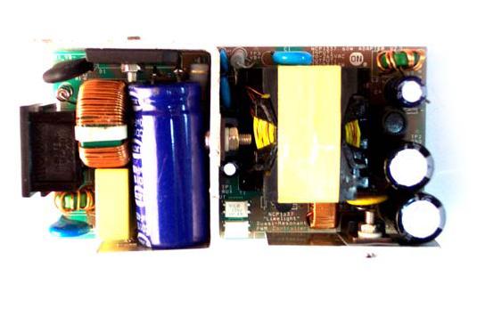

9 BOARD PICTURES 9

10 SCHEMATIC 10


11 BOARD LAYOUT Figure 13. Assembly Drawing Figure 14. Global Layer Figure 15. Top Layer 11

12 BOARD LAYOUT Figure 16. Bottom Layer Table 2. BILL OF MATERIALS Item Quantity Reference Part Manufacturer 1 1 C1 2.2 nf/y1 2 2 C2, C F, 16 V 3 1 C4 470 F, 16 V 4 1 C5 4.7 nf, 1 kv 5 1 C F/X2 6 1 C7 150 F, 400 V 7 1 C8 10 nf, 1 kv 8 1 C9 2.2 nf, 100 V 9 1 C10 1 nf, 50 V 10 4 C11, C13, C14, C F, 50 V 11 1 C12 47 F, 25 V 12 1 C pf, 50 V 13 1 D1 GBU D2 MBR160 ON Semiconductor 15 1 D3 1N4937 ON Semiconductor 16 3 D4, D7, D8 MMSD4148 ON Semiconductor 17 1 D5 MMSZ13 ON Semiconductor 18 1 D6 MMSZ15 ON Semiconductor 19 1 F1 T3A250VAC 20 1 L1 1.8 H, 5A 21 1 L2 75 H 22 1 L3 150 H 23 1 L4 20 mh 24 1 Q1 NTP75N06 ON Semiconductor 25 4 Q2, Q5, Q6, Q8 MMBT3906L ON Semiconductor 26 1 Q3 9 A, 650 V 27 2 Q4, Q7 MMBT3906L ON Semiconductor 12
13 Table 2. BILL OF MATERIALS Item Quantity Reference Part Manufacturer 28 1 R1 5 NTC 29 4 R2, R6, R10, R19 1M 30 1 R3 MOV R4 47k /1 W 32 1 R R7, R15, R18 2 k 34 4 R8, R22, R26, R k 35 4 R9, R20, R29, R32 10 k 36 2 R11, R R12, R14, R16, R24, R25 1 k 38 1 R13 15 k 39 1 R17 20 k 40 1 R R k 42 1 R k 43 1 R /1 W 44 1 T1 PQ T2 CT1:100 Toroid or UU U1, U2 PC817C 47 1 U3 NCP1337 ON Semiconductor 48 1 U4 TL431A ON Semiconductor 49 1 PCB PCB5.2*10 Appendix Product Information NCP1337 Quasi Resonant Controller featuring Over Power Compensation TL431A Programmable Precision Reference 1N4937 Fast-Recovery Rectifier, 1 A, 600 V MBR160 Schottky Rectifier, 1 A, 60 V MMBT3904L General Purpose Transisitor, NPN MMBT3906L General Purpose Transisitor, PNP MMSD4148 Switching Diode MMSZ13 Zener Diode, 500 mw, 13 V MMSZ15 Zener Diode, 500 mw, 15 V NTP75N06 Power MOSFET, 75 A, 60 V References CECP (China): Energy Saving (Korea): Top Runner (Japan): EU Eco-label (Europe): en.htm t/pg_portablecomputers_en.htm EU Code of Conduct (Europe): tive.htm GEEA (Europe): Energy Star: plies.power_supplies_consumers 1 Watt Executive Order:
14 Transformer Specification LP (W1 + W4) = 600 H 10 khz 1 V Leaking Induction: 60 H max CORE: PQ32 20 Pin1 Pin2 W4 Pin10,11,12 W2,W5 Secondary Side Pin7,8,9 W1 Primary Side Pin3 Pin4 W3 Pin5 T1 PQ3220 GreenPoint is a registered trademark of Semiconductor Components Industries, LLC (SCILLC). ON Semiconductor and are registered trademarks of Semiconductor Components Industries, LLC (SCILLC). SCILLC owns the rights to a number of patents, trademarks, copyrights, trade secrets, and other intellectual property. A listing of SCILLC s product/patent coverage may be accessed at Marking.pdf. SCILLC reserves the right to make changes without further notice to any products herein. SCILLC makes no warranty, representation or guarantee regarding the suitability of its products for any particular purpose, nor does SCILLC assume any liability arising out of the application or use of any product or circuit, and specifically disclaims any and all liability, including without limitation special, consequential or incidental damages. Typical parameters which may be provided in SCILLC data sheets and/or specifications can and do vary in different applications and actual performance may vary over time. All operating parameters, including Typicals must be validated for each customer application by customer s technical experts. SCILLC does not convey any license under its patent rights nor the rights of others. SCILLC products are not designed, intended, or authorized for use as components in systems intended for surgical implant into the body, or other applications intended to support or sustain life, or for any other application in which the failure of the SCILLC product could create a situation where personal injury or death may occur. Should Buyer purchase or use SCILLC products for any such unintended or unauthorized application, Buyer shall indemnify and hold SCILLC and its officers, employees, subsidiaries, affiliates, and distributors harmless against all claims, costs, damages, and expenses, and reasonable attorney fees arising out of, directly or indirectly, any claim of personal injury or death associated with such unintended or unauthorized use, even if such claim alleges that SCILLC was negligent regarding the design or manufacture of the part. SCILLC is an Equal Opportunity/Affirmative Action Employer. This literature is subject to all applicable copyright laws and is not for resale in any manner. PUBLICATION ORDERING INFORMATION LITERATURE FULFILLMENT: Literature Distribution Center for ON Semiconductor P.O. Box 5163, Denver, Colorado USA Phone: or Toll Free USA/Canada Fax: or Toll Free USA/Canada orderlit@onsemi.com N. American Technical Support: Toll Free USA/Canada Europe, Middle East and Africa Technical Support: Phone: Japan Customer Focus Center Phone: ON Semiconductor Website: Order Literature: For additional information, please contact your local Sales Representative EVBUM2075/D
EVALUATION BOARD FOR STK N, 120N, 140N. Phenol 1-layer Board) Figure 2. STK NGEVB Figure 3. STK NGEVB Figure 4.
 Figure 2. STK NGEVB Figure 3. STK NGEVB Figure 4.") STK44-NGEVB, STK44-1NGEVB, STK44-14NGEVB STK44-N Series Evaluation Board User's Manual EVAL BOARD USER S MANUAL Thick-Film Hybrid IC for use used in from 6 W to 18 W 1ch class AB audio power amplifiers.
STK44-NGEVB, STK44-1NGEVB, STK44-14NGEVB STK44-N Series Evaluation Board User's Manual EVAL BOARD USER S MANUAL Thick-Film Hybrid IC for use used in from 6 W to 18 W 1ch class AB audio power amplifiers.
AND8285/D. NCP1521B Adjustable Output Voltage Step Down Converter Simulation Procedure SIMULATION NOTE
 NCP1521B Adjustable Output Voltage Step Down Converter Simulation Procedure Prepared by: Bertrand Renaud On Semiconductor SIMULATION NOTE Overview The NCP1521B step down PWM DC DC converter is optimized
1. DEFINE THE SPECIFICATION 2. SELECT A TOPOLOGY
 How to Choose for Design This article is to present a way to choose a switching controller for design in the s Selector Guide SGD514/D from ON Semiconductor. (http://www.onsemi.com/pub/collateral/sgd514d.pdf)
AND8246/D. A 160 W CRT TV Power Supply using NCP1337 APPLICATION NOTE. A 160 W TV Power Supply Design
 A 10 W CRT TV Power Supply using NCP1337 Prepared by: Nicolas Cyr ON Semiconductor APPLICATION NOTE Introduction Valley switching converters, also known as quasi resonant (QR) converters, allow designing
AND9043/D. An Off-Line, Power Factor Corrected, Buck-Boost Converter for Low Power LED Applications APPLICATION NOTE.
 An Off-Line, Power Factor Corrected, Buck-Boost Converter for Low Power LED Applications Prepared by: Frank Cathell ON Semiconductor Introduction This application note introduces a universal input, off
NCP1207AADAPGEVB. Implementing NCP1207 in QR 24 W AC-DC Converter with Synchronous Rectifier Evaluation Board User's Manual EVAL BOARD USER S MANUAL
 NCP07AADAPGEVB Implementing NCP07 in QR 4 W AC-DC Converter with Synchronous Rectifier Evaluation Board User's Manual EVAL BOARD USER S MANUAL Introduction The NCP07 is a controller dedicated for driving
Low Capacitance Transient Voltage Suppressors / ESD Protectors CM QG/D. Features
 Low Capacitance Transient Voltage Suppressors / ESD Protectors CM1250-04QG Features Low I/O capacitance at 5pF at 0V In-system ESD protection to ±8kV contact discharge, per the IEC 61000-4-2 international
NTNS3164NZT5G. Small Signal MOSFET. 20 V, 361 ma, Single N Channel, SOT 883 (XDFN3) 1.0 x 0.6 x 0.4 mm Package
 1.0 x 0.6 x 0.4 mm Package") NTNS36NZ Small Signal MOSFET V, 36 ma, Single N Channel, SOT 883 (XDFN3). x.6 x. mm Package Features Single N Channel MOSFET Ultra Low Profile SOT 883 (XDFN3). x.6 x. mm for Extremely Thin Environments
NTNS36NZ Small Signal MOSFET V, 36 ma, Single N Channel, SOT 883 (XDFN3). x.6 x. mm Package Features Single N Channel MOSFET Ultra Low Profile SOT 883 (XDFN3). x.6 x. mm for Extremely Thin Environments
NTK3139P. Power MOSFET. 20 V, 780 ma, Single P Channel with ESD Protection, SOT 723
 NTK9P Power MOSFET V, 78 ma, Single P Channel with ESD Protection, SOT 7 Features P channel Switch with Low R DS(on) % Smaller Footprint and 8% Thinner than SC 89 Low Threshold Levels Allowing.5 V R DS(on)
PCS2I2309NZ. 3.3 V 1:9 Clock Buffer
 . V 1:9 Clock Buffer Functional Description PCS2I209NZ is a low cost high speed buffer designed to accept one clock input and distribute up to nine clocks in mobile PC systems and desktop PC systems. The
NVLJD4007NZTBG. Small Signal MOSFET. 30 V, 245 ma, Dual, N Channel, Gate ESD Protection, 2x2 WDFN Package
 NVLJD7NZ Small Signal MOSFET V, 2 ma, Dual, N Channel, Gate ESD Protection, 2x2 WDFN Package Features Optimized Layout for Excellent High Speed Signal Integrity Low Gate Charge for Fast Switching Small
Is Now Part of To learn more about ON Semiconductor, please visit our website at
 Is Now Part of To learn more about ON Semiconductor, please visit our website at www.onsemi.com ON Semiconductor and the ON Semiconductor logo are trademarks of Semiconductor Components Industries, LLC
NSR0340V2T1/D. Schottky Barrier Diode 40 VOLT SCHOTTKY BARRIER DIODE
 Schottky Barrier Diode Schottky barrier diodes are optimized for very low forward voltage drop and low leakage current and are used in a wide range of dc dc converter, clamping and protection applications
NCP800. Lithium Battery Protection Circuit for One Cell Battery Packs
 Lithium Battery Protection Circuit for One Cell Battery Packs The NCP800 resides in a lithium battery pack where the battery cell continuously powers it. In order to maintain cell operation within specified
NTTFS3A08PZTWG. Power MOSFET 20 V, 15 A, Single P Channel, 8FL
 NTTFS3A8PZ Power MOSFET V, 5 A, Single P Channel, 8FL Features Ultra Low R DS(on) to Minimize Conduction Losses 8FL 3.3 x 3.3 x.8 mm for Space Saving and Excellent Thermal Conduction ESD Protection Level
AND8291/D. >85% Efficient 12 to 5 VDC Buck Converter
 >5% Efficient to 5 VDC Buck Converter Prepared by: DENNIS SOLLEY ON Semiconductor General Description This application note describes how the NCP363 can be configured as a buck controller to drive an external
Is Now Part of To learn more about ON Semiconductor, please visit our website at
 Is Now Part of To learn more about ON Semiconductor, please visit our website at www.onsemi.com ON Semiconductor and the ON Semiconductor logo are trademarks of Semiconductor Components Industries, LLC
Is Now Part of To learn more about ON Semiconductor, please visit our website at
 Is Now Part of To learn more about ON Semiconductor, please visit our website at www.onsemi.com ON Semiconductor and the ON Semiconductor logo are trademarks of Semiconductor Components Industries, LLC
PIN CONNECTIONS MAXIMUM RATINGS (T J = 25 C unless otherwise noted) SC 75 (3 Leads) Parameter Symbol Value Unit Drain to Source Voltage V DSS 30 V
 SC 75 (3 Leads) Parameter Symbol Value Unit Drain to Source Voltage V DSS 30 V") NTA7N, NVTA7N Small Signal MOSFET V, 4 ma, Single, N Channel, Gate ESD Protection, SC 7 Features Low Gate Charge for Fast Switching Small.6 x.6 mm Footprint ESD Protected Gate NV Prefix for Automotive
NTA7N, NVTA7N Small Signal MOSFET V, 4 ma, Single, N Channel, Gate ESD Protection, SC 7 Features Low Gate Charge for Fast Switching Small.6 x.6 mm Footprint ESD Protected Gate NV Prefix for Automotive
AND9100/D. Paralleling of IGBTs APPLICATION NOTE. Isothermal point
 Paralleling of IGBTs Introduction High power systems require the paralleling of IGBTs to handle loads well into the 10 s and sometimes the 100 s of kilowatts. Paralleled devices can be discrete packaged
NTK3043N. Power MOSFET. 20 V, 285 ma, N Channel with ESD Protection, SOT 723
 NTKN Power MOSFET V, 8 ma, N Channel with ESD Protection, SOT 7 Features Enables High Density PCB Manufacturing % Smaller Footprint than SC 89 and 8% Thinner than SC 89 Low Voltage Drive Makes this Device
NCP59302, NCV A, Very Low-Dropout (VLDO) Fast Transient Response Regulator series
 Fast Transient Response Regulator series") NCP5932, NCV5932 3. A, Very Low-Dropout (VLDO) Fast Transient Response Regulator series The NCP5932 is a high precision, very low dropout (VLDO), low ground current positive voltage regulator that is capable
NCP5932, NCV5932 3. A, Very Low-Dropout (VLDO) Fast Transient Response Regulator series The NCP5932 is a high precision, very low dropout (VLDO), low ground current positive voltage regulator that is capable
NTJD1155LT1G. Power MOSFET. 8 V, 1.3 A, High Side Load Switch with Level Shift, P Channel SC 88
 NTJDL Power MOSFET V,.3 A, High Side Load Switch with Level Shift, P Channel SC The NTJDL integrates a P and N Channel MOSFET in a single package. This device is particularly suited for portable electronic
NTD5865NL. N-Channel Power MOSFET 60 V, 46 A, 16 m
 N-Channel Power MOSFET 6 V, 6 A, 6 m Features Low Gate Charge Fast Switching High Current Capability % Avalanche Tested These Devices are Pb Free, Halogen Free and are RoHS Compliant MAXIMUM RATINGS (
NTGS3441BT1G. Power MOSFET. -20 V, -3.5 A, Single P-Channel, TSOP-6. Low R DS(on) in TSOP-6 Package 2.5 V Gate Rating This is a Pb-Free Device
 in TSOP-6 Package 2.5 V Gate Rating This is a Pb-Free Device") Power MOSFET - V, -. A, Single P-Channel, TSOP- Features Low R DS(on) in TSOP- Package. V Gate Rating This is a Pb-Free Device Applications Battery Switch and Load Management Applications in Portable Equipment
Power MOSFET - V, -. A, Single P-Channel, TSOP- Features Low R DS(on) in TSOP- Package. V Gate Rating This is a Pb-Free Device Applications Battery Switch and Load Management Applications in Portable Equipment
2N6667, 2N6668. Darlington Silicon Power Transistors PNP SILICON DARLINGTON POWER TRANSISTORS 10 A, V, 65 W
 Darlington Silicon Power Transistors Designed for general purpose amplifier and low speed switching applications. High DC Current Gain h FE = 500 (Typ) @ I C =.0 Adc Collector Emitter Sustaining Voltage
NUF8401MNT4G. 8-Channel EMI Filter with Integrated ESD Protection
 8-Channel EMI Filter with Integrated ESD Protection The NUF841MN is an eight channel (C R C) Pi style EMI filter array with integrated ESD protection. Its typical component values of R = 1 and C = 12 pf
NCP57302, NCV A, Very Low-Dropout (VLDO) Fast Transient Response Regulator
 Fast Transient Response Regulator") NCP5732, NC5732 3. A, ery Low-Dropout (LDO) Fast Transient Response Regulator The NCP5732 is a high precision, very low dropout (LDO), low minimum input voltage and low ground current positive voltage
NCP5732, NC5732 3. A, ery Low-Dropout (LDO) Fast Transient Response Regulator The NCP5732 is a high precision, very low dropout (LDO), low minimum input voltage and low ground current positive voltage
AND8312/D. A 36W Ballast Application with the NCP5104
 A 6W Ballast Application with the P50 Prepared by: Thierry Sutto This document describes how the P50 driver can be implemented in a ballast application. The scope of this application note is to highlight
NUF4401MNT1G. 4-Channel EMI Filter with Integrated ESD Protection
 4-Channel EMI Filter with Integrated ESD Protection The is a four channel (C R C) Pi style EMI filter array with integrated ESD protection. Its typical component values of R = 200 and C = 5 pf deliver
NTHD4502NT1G. Power MOSFET. 30 V, 3.9 A, Dual N Channel ChipFET
 NTHDN Power MOSFET V,.9 A, Dual N Channel ChipFET Features Planar Technology Device Offers Low R DS(on) and Fast Switching Speed Leadless ChipFET Package has % Smaller Footprint than TSOP. Ideal Device
FJP13007 High Voltage Fast-Switching NPN Power Transistor
 FJP3007 High Voltage Fast-Switching NPN Power Transistor Features High Voltage High Speed Power Switch Application High Voltage Capability High Switching Speed Suitable for Electronic Ballast and Switching
NTNUS3171PZ. Small Signal MOSFET. 20 V, 200 ma, Single P Channel, 1.0 x 0.6 mm SOT 1123 Package
 NTNUS7PZ Small Signal MOSFET V, ma, Single P Channel,. x.6 mm SOT Package Features Single P Channel MOSFET Offers a Low R DS(on) Solution in the Ultra Small. x.6 mm Package. V Gate Voltage Rating Ultra
2N5194G, 2N5195G. Silicon PNP Power Transistors 4 AMPERE POWER TRANSISTORS PNP SILICON VOLTS
 , Silicon PNP Power Transistors These devices are designed for use in power amplifier and switching circuits; excellent safe area limits. Features Complement to NPN 2N5191, 2N5192 These Devices are PbFree
CAX803, CAX809, CAX Pin Microprocessor Power Supply Supervisors
 3-Pin Microprocessor Power Supply Supervisors Description The CAX83, CAX89, and CAX81 are supervisory circuits that monitor power supplies in digital systems. The CAX83, CAX89, and CAX81 are direct replacements
AND8450/D. NCV7680 LED Driver Linear Regulator Performance APPLICATION NOTE
 NCV7680 LED Driver Linear Regulator Performance APPLICATION NOTE Introduction The NCV7680 is an automotive LED driver targeted primarily for rear combination lamp systems. A high input voltage to this
MBR735, MBR745. SWITCHMODE Power Rectifiers. SCHOTTKY BARRIER RECTIFIERS 7.5 AMPERES 35 and 45 VOLTS
 MBR735, MBR75 SWITCHMODE Power Rectifiers Features and Benefits Low Forward Voltage Low Power Loss/High Efficiency High Surge Capacity 75 C Operating Junction Temperature PbFree Packages are Available*
MBR130LSFT1G. Surface Mount Schottky Power Rectifier. Plastic SOD 123 Package SCHOTTKY BARRIER RECTIFIER 1.0 AMPERES, 30 VOLTS
 MBR3LSFTG Surface Mount Schottky Power Rectifier Plastic SOD 23 Package This device uses the Schottky Barrier principle with a large area metal to silicon power diode. Ideally suited for low voltage, high
NCP5425DEMO/D. NCP5425 Demonstration Board Note. Single Input to Dual Output Buck Regulator 5.0 V to 1.5 V/15 A and 1.8 V/15 A DEMONSTRATION NOTE
 NCP5425 Demonstration Board Note Single Input to Dual Output Buck Regulator 5.0 V to 1.5 V/15 A and 1.8 V/15 A DEMONSTRATION NOTE Description The NCP5425 demonstration board is a 4.0 by 4.0, two layer
Extended V GSS range ( 25V) for battery applications
 for battery applications") Dual Volt P-Channel PowerTrench MOSFET General Description This P-Channel MOSFET has been designed specifically to improve the overall efficiency of DC/DC converters using either synchronous or conventional
Dual Volt P-Channel PowerTrench MOSFET General Description This P-Channel MOSFET has been designed specifically to improve the overall efficiency of DC/DC converters using either synchronous or conventional
MBR20200CT. Switch mode Power Rectifier. Dual Schottky Rectifier SCHOTTKY BARRIER RECTIFIER 20 AMPERES, 200 VOLTS
 MBRCT Switch mode Power Rectifier Dual Schottky Rectifier Features and Benefits Low Forward Voltage Low Power Loss/High Efficiency High Surge Capacity 75 C Operating Junction Temperature A Total ( A Per
P2042A LCD Panel EMI Reduction IC
 LCD Panel EMI Reduction IC Features FCC approved method of EMI attenuation Provides up to 15dB of EMI suppression Generates a low EMI spread spectrum clock of the input frequency Input frequency range:
NCP5504, NCV ma Dual Output Low Dropout Linear Regulator
 25 ma Dual Output Low Dropout Linear Regulator The NCP554/NCV554 are dual output low dropout linear regulators with 2.% accuracy over the operating temperature range. They feature a fixed output voltage
Figure 1. NCP5104 Evaluation Board
 P50 6 W Ballast Evaluation Board User's Manual EVAL BOARD USER S MANUAL Introduction This document describes how the P50 driver can be implemented in a ballast application. The scope of this evaluation
NSVEMD4DXV6T5G. Dual Bias Resistor Transistors. NPN and PNP Silicon Surface Mount Transistors with Monolithic Bias Resistor Network
 Dual Bias Resistor Transistors NPN and PNP Silicon Surface Mount Transistors with Monolithic Bias Resistor Network The BRT (Bias Resistor Transistor) contains a single transistor with a monolithic bias
Parameter Symbol Conditions Ratings Unit
 Ordering number : ENN8386 Monolithic Linear IC Downconverter IC for Digital CATV http://onsemi.com Overview The is a downconverter IC for digital CATV. It accepts RF input frequencies from 50 to 150MHz
FGH40N60SFDTU-F V, 40 A Field Stop IGBT
 FGH40N60SFDTU-F085 600 V, 40 A Field Stop IGBT Features High Current Capability Low Saturation Voltage: V CE(sat) = 2.3 V @ I C = 40 A High Input Impedance Fast Switching RoHS Compliant Qualified to Automotive
Single stage LNA for GPS Using the MCH4009 Application Note
 Single stage LNA for GPS Using the MCH49 Application Note http://onsemi.com Overview This application note explains about ON Semiconductor s MCH49 which is used as a Low Noise Amplifier (LNA) for GPS (Global
MURS120T3G Series, SURS8120T3G Series. Surface Mount Ultrafast Power Rectifiers
 MURS12T3G Series, SURS812T3G Series Surface Mount Ultrafast Power Rectifiers MURS5T3G, MURS1T3G, MURS115T3G, MURS12T3G, MURS14T3G, MURS16T3G, SURS85T3G, SURS81T3G, SURS8115T3G, SURS812T3G, SURS814T3G,
NTA4153N, NTE4153N, NVA4153N, NVE4153N. Small Signal MOSFET. 20 V, 915 ma, Single N Channel with ESD Protection, SC 75 and SC 89
 NTA45N, NTE45N, NVA45N, NVE45N Small Signal MOSFET V, 95 ma, Single N Channel with ESD Protection, SC 75 and SC 89 Features Low R DS(on) Improving System Efficiency Low Threshold Voltage,.5 V Rated ESD
General Description. Applications. Power management Load switch Q2 3 5 Q1
 FDG6342L Integrated Load Switch Features Max r DS(on) = 150mΩ at V GS = 4.5V, I D = 1.5A Max r DS(on) = 195mΩ at V GS = 2.5V, I D = 1.3A Max r DS(on) = 280mΩ at V GS = 1.8V, I D = 1.1A Max r DS(on) = 480mΩ
Overview The LA5744MP is a separately-excited step-down switching regulator (variable type).
.") Ordering number : ENA0587A Monolithic Linear IC Separately-Excited Step-Down Switching Regulator (Variable Type) http://onsemi.com Overview The is a separately-excited step-down switching regulator (variable
Ordering number : ENA0587A Monolithic Linear IC Separately-Excited Step-Down Switching Regulator (Variable Type) http://onsemi.com Overview The is a separately-excited step-down switching regulator (variable
NCV887300LEDGEVB. NCV Automotive Grade High frequency Dimmable LED Boost Controller Evaluation Board User's Manual EVAL BOARD USER S MANUAL
 NCV887300 Automotive Grade High frequency Dimmable LED Boost Controller Evaluation Board User's Manual EVAL BOARD USER S MANUAL Description This NCV887300 evaluation board provides a convenient way to
NLAS5157. Ultra-Low 0.4 SPDT Analog Switch
 Ultra-Low.4 SPDT Analog Switch The NLAS5157 is Single Pole Double Throw (SPDT) switch designed for audio systems in portable applications. The NLAS5157 features Ultra Low R ON of.4 typical at = V and.15
FDPC4044. Common Drain N-Channel PowerTrench MOSFET. FDPC4044 Common Drain N-Channel PowerTrench MOSFET. 30 V, 27 A, 4.
 FDPC444 Common Drain N-Channel PowerTrench MOSFET 3 V, 7 A, 4.3 mω Features Max r SS(on) = 4.3 mω at V GS = V, I SS = 7 A Max r SS(on) = 6.4 mω at V GS = 4.5 V, I SS = 3 A Pakage size/height: 3.3 x 3.3
NTGD4167C. Power MOSFET Complementary, 30 V, +2.9/ 2.2 A, TSOP 6 Dual
 Power MOSFET Complementary, 3 V, +.9/. A, TSOP 6 Dual Features Complementary N Channel and P Channel MOSFET Small Size (3 x 3 mm) Dual TSOP 6 Package Leading Edge Trench Technology for Low On Resistance
MBD110DWT1G MBD330DWT1G. Dual Schottky Barrier Diodes
 , Dual Schottky Barrier Diodes Application circuit designs are moving toward the consolidation of device count and into smaller packages. The new SOT363 package is a solution which simplifies circuit design,
MRA4003T3G Series, NRVA4003T3G Series. Surface Mount Standard Recovery Power Rectifier. SMA Power Surface Mount Package
 MRA43T3G Series, NRVA43T3G Series Surface Mount Standard Recovery Power Rectifier Power Surface Mount Package Features construction with glass passivation. Ideally suited for surface mounted automotive
FGH12040WD 1200 V, 40 A Field Stop Trench IGBT
 FGH12040WD 1200 V, 40 A Field Stop Trench IGBT Features Maximum Junction Temperature : T J = 175 o C Positive Temperature Co-efficient for Easy Parallel Operating Low Saturation Voltage: V CE(sat) = 2.3
 Distributed by: www.jameco.com 1-800-831-44 The content and copyrights of the attached material are the property of its owner. Transient Voltage Suppressors Micro Packaged Diodes for ESD Protection The
FFSH5065A. Silicon Carbide Schottky Diode 650 V, 50 A
 Silicon Carbide Schottky Diode 65 V, 5 A Description Silicon Carbide (SiC) Schottky Diodes use a completely new technology that provides superior switching performance and higher reliability compared to
FDS8984 N-Channel PowerTrench MOSFET 30V, 7A, 23mΩ
 FDS898 N-Channel PowerTrench MOSFET V, 7A, 3mΩ General Description This N-Channel MOSFET has been designed specifically to improve the overall efficiency of DC/DC converters using either synchronous or
MBRA320T3G Surface Mount Schottky Power Rectifier
 Surface Mount Schottky Power Rectifier Power Surface Mount Package Employing the Schottky Barrier principle in a large area metal to silicon power diode. State of the art geometry features epitaxial construction
NTD5867NL. N-Channel Power MOSFET 60 V, 20 A, 39 m
 N-Channel Power MOSFET 6 V, A, 39 m Features Low R DS(on) High Current Capability % Avalanche Tested These Devices are Pb Free, Halogen Free/BFR Free and are RoHS Compliant MAXIMUM RATINGS ( unless otherwise
DEMONSTRATION NOTE. Figure 1. CS51411/3 Demonstration Board. 1 Publication Order Number: CS51411DEMO/D
 DEMONSTRATION NOTE Description The CS51411 demonstration board is a 1.0 A/3.3 V buck regulator running at 260 khz (CS51411) or 520 khz (CS51413). The switching frequency can be synchronized to a higher
Is Now Part of To learn more about ON Semiconductor, please visit our website at
 Is Now Part of To learn more about ON Semiconductor, please visit our website at www.onsemi.com ON Semiconductor and the ON Semiconductor logo are trademarks of Semiconductor Components Industries, LLC
NTA4001N, NVA4001N. Small Signal MOSFET. 20 V, 238 ma, Single, N Channel, Gate ESD Protection, SC 75
 Small Signal MOSFET V, 8 ma, Single, N Channel, Gate ESD Protection, SC 75 Features Low Gate Charge for Fast Switching Small.6 x.6 mm Footprint ESD Protected Gate AEC Q Qualified and PPAP Capable NVA4N
BAV103 High Voltage, General Purpose Diode
 BAV3 High Voltage, General Purpose Diode Cathode Band SOD80 Description A general purpose diode that couples high forward conductance fast swiching speed and high blocking voltages in a glass leadless
AND8388/D. Input Dynamic Range Extension of the BelaSigna 300 Series
 Input Dynamic Range Extension of the BelaSigna 300 Series INTRODUCTION This application note describes the functioning of the BelaSigna 300 input dynamic range extension (IDRX) feature. The goal of this
NCP A Low Dropout Linear Regulator
 1.5 A Low Dropout Linear Regulator The NCP566 low dropout linear regulator will provide 1.5 A at a fixed output voltage. The fast loop response and low dropout voltage make this regulator ideal for applications
FDS8935. Dual P-Channel PowerTrench MOSFET. FDS8935 Dual P-Channel PowerTrench MOSFET. -80 V, -2.1 A, 183 mω
 FDS935 Dual P-Channel PowerTrench MOSFET - V, -. A, 3 mω Features Max r DS(on) = 3 mω at V GS = - V, I D = -. A Max r DS(on) = 7 mω at V GS = -.5 V, I D = -.9 A High performance trench technology for extremely
BD809 (NPN), BD810 (PNP) Plastic High Power Silicon Transistor 10 AMPERE POWER TRANSISTORS 80 VOLTS 90 WATTS
, BD810 (PNP) Plastic High Power Silicon Transistor 10 AMPERE POWER TRANSISTORS 80 VOLTS 90 WATTS") BD89 (NPN), BD8 (PNP) Plastic High Power Silicon Transistor These devices are designed for use in high power audio amplifiers utilizing complementary or quasi complementary circuits. Features DC Current
BD89 (NPN), BD8 (PNP) Plastic High Power Silicon Transistor These devices are designed for use in high power audio amplifiers utilizing complementary or quasi complementary circuits. Features DC Current
SS13FL, SS14FL. Surface Mount Schottky Barrier Rectifier
 SS13FL, SS14FL Surface Mount Schottky Barrier Rectifier Features Ultra Thin Profile Maximum Height of 1.08 mm UL Flammability 94V 0 Classification MSL 1 Green Mold Compound These Devices are Pb Free, Halogen
P-Channel PowerTrench MOSFET
 FDD4685-F085 P-Channel PowerTrench MOSFET -40 V, -32 A, 35 mω Features Typical R DS(on) = 23 m at V GS = -10V, I D = -8.4 A Typical R DS(on) = 30 m at V GS = -4.5V, I D = -7 A Typical Q g(tot) = 19 nc
MURS320T3G, SURS8320T3G, MURS340T3G, SURS8340T3G, MURS360T3G, SURS8360T3G. Surface Mount Ultrafast Power Rectifiers
 MURS32T3G, SURS832T3G, MURS34T3G, SURS834T3G, MURS36T3G, Surface Mount Ultrafast Power Rectifiers This series employs the state of the art epitaxial construction with oxide passivation and metal overlay
NUS2045MN, NUS3045MN. Overvoltage Protection IC with Integrated MOSFET
 , Overvoltage Protection IC with Integrated MOSFET These devices represent a new level of safety and integration by combining the NCP34 overvoltage protection circuit (OVP) with a 2 V P channel power MOSFET
NCP786L. Wide Input Voltage Range 5 ma Ultra-Low Iq, High PSRR Linear Regulator with Adjustable Output Voltage
 Wide Input Voltage Range 5 ma Ultra-Low Iq, High PSRR Linear Regulator with Adjustable Output Voltage The is high performance linear regulator, offering a very wide operating input voltage range of up
RURG8060-F085 80A, 600V Ultrafast Rectifier
 RURG86F85 8A, 6V Ultrafast Rectifier Features High Speed Switching ( t rr =74ns(Typ.) @ I F =8A ) Low Forward Voltage( V F =.34V(Typ.) @ I F =8A ) Avalanche Energy Rated AECQ Qaulified Applications Automotive
BD809 (NPN), BD810 (PNP) Plastic High Power Silicon Transistors 10 AMPERE POWER TRANSISTORS 80 VOLTS 90 WATTS
, BD810 (PNP) Plastic High Power Silicon Transistors 10 AMPERE POWER TRANSISTORS 80 VOLTS 90 WATTS") BD89 (NPN), BD8 (PNP) Plastic High Power Silicon Transistors These devices are designed for use in high power audio amplifiers utilizing complementary or quasi complementary circuits. Features High DC
BD89 (NPN), BD8 (PNP) Plastic High Power Silicon Transistors These devices are designed for use in high power audio amplifiers utilizing complementary or quasi complementary circuits. Features High DC
NSVJ3910SB3 N-Channel JFET 25V, 20 to 40mA, 40mS
 NSVJ910SB N-Channel JFET 25V, 20 to 40mA, 40mS Automotive JFET designed for compact and efficient designs and including high gain performance. AEC-Q101 qualified JFET and PPAP capable suitable for automotive
NVTFS4C13N. Power MOSFET. 30 V, 9.4 m, 40 A, Single N Channel, 8FL Features
 NVTFS4C3N Power MOSFET 3 V, 9.4 m, 4 A, Single N Channel, 8FL Features Low R DS(on) to Minimize Conduction Losses Low Capacitance to Minimize Driver Losses Optimized Gate Charge to Minimize Switching Losses
Bottom. Pin 1 S S S D D D. Symbol Parameter Ratings Units V DS Drain to Source Voltage 30 V V GS Gate to Source Voltage (Note 4) ±20 V
 ±20 V") D D D FDMS7658AS N-Channel PowerTrench SyncFET TM 3 V, 76 A,.9 mω Features Max r DS(on) =.9 mω at V GS = V, I D = 8 A Max r DS(on) =. mω at V GS = 7 V, I D = 6 A Advanced Package and Silicon Combination
D D D FDMS7658AS N-Channel PowerTrench SyncFET TM 3 V, 76 A,.9 mω Features Max r DS(on) =.9 mω at V GS = V, I D = 8 A Max r DS(on) =. mω at V GS = 7 V, I D = 6 A Advanced Package and Silicon Combination
NTMFS4936NCT3G. NTMFS4936NC Power MOSFET 30 V, 79 A, Single N Channel, SO 8 FL
 NTMFS4936N, NTMFS4936NC Power MOSFET 3 V, 79 A, Single N Channel, Features Low R S(on), Low Capacitance and Optimized Gate Charge to Minimize Conduction, river and Switching Losses Next Generation Enhanced
NTS4172NT1G. Power MOSFET. 30 V, 1.7 A, Single N Channel, SC 70. Low On Resistance Low Gate Threshold Voltage Halide Free This is a Pb Free Device
 Power MOSFET V,.7 A, Single N Channel, SC 7 Features Low On Resistance Low Gate Threshold Voltage Halide Free This is a Pb Free Device V (BR)DSS R DS(on) MAX I D MAX Applications Low Side Load Switch DC
PCS2P2309/D. 3.3V 1:9 Clock Buffer. Functional Description. Features. Block Diagram
 3.3V 1:9 Clock Buffer Features One-Input to Nine-Output Buffer/Driver Buffers all frequencies from DC to 133.33MHz Low power consumption for mobile applications Less than 32mA at 66.6MHz with unloaded
Is Now Part of To learn more about ON Semiconductor, please visit our website at
 Is Now Part of To learn more about ON Semiconductor, please visit our website at www.onsemi.com ON Semiconductor and the ON Semiconductor logo are trademarks of Semiconductor Components Industries, LLC
Dual N-Channel, Digital FET
 FDG6301N-F085 Dual N-Channel, Digital FET Features 25 V, 0.22 A continuous, 0.65 A peak. R DS(ON) = 4 @ V GS = 4.5 V, R DS(ON) = 5 @ V GS = 2.7 V. Very low level gate drive requirements allowing directoperation
NGTB15N60EG. IGBT - Short-Circuit Rated. 15 A, 600 V V CEsat = 1.7 V
 NGTB5N6EG IGBT - Short-Circuit Rated This Insulated Gate Bipolar Transistor (IGBT) features a robust and cost effective NonPunch Through (NPT) Trench construction, and provides superior performance in
Is Now Part of To learn more about ON Semiconductor, please visit our website at
 Is Now Part of To learn more about ON Semiconductor, please visit our website at www.onsemi.com ON Semiconductor and the ON Semiconductor logo are trademarks of Semiconductor Components Industries, LLC
434MHz LNA for RKE Using the 2SC5245A Application Note
 434MHz LNA for RKE Using the 2SC5245A Application Note http://onsemi.com Overview This application note explains about ON Semiconductor s 2SC5245A which is used as a Low Noise Amplifier (LNA) for RKE (Remote
NCL30000LED2GEVB/D Vac up to 15 Watt Dimmable LED Driver Demo Board Operation EVALUATION BOARD MANUAL
 180-265 Vac up to 15 Watt Dimmable LED Driver Demo Board Operation Prepared by: Jim Young ON Semiconductor EVALUATION BOARD MANUAL Introduction The NCL30000 is a power factor corrected LED driver controller.
AND8289. LED Driving with NCP/V3063
 LE riving with NCP/V3063 Prepared by: Petr Konvicny, Bernie Weir ON Semiconductor Introduction Improvements in high brightness LEs present the potential for creative new lighting solutions that offer an
NTTFS5820NLTWG. Power MOSFET. 60 V, 37 A, 11.5 m. Low R DS(on) Low Capacitance Optimized Gate Charge These Devices are Pb Free and are RoHS Compliant
 Low Capacitance Optimized Gate Charge These Devices are Pb Free and are RoHS Compliant") NTTFS582NL Power MOSFET 6 V, 37 A,.5 m Features Low R DS(on) Low Capacitance Optimized Gate Charge These Devices are Pb Free and are RoHS Compliant MAXIMUM RATINGS ( unless otherwise stated) Parameter
NTTFS582NL Power MOSFET 6 V, 37 A,.5 m Features Low R DS(on) Low Capacitance Optimized Gate Charge These Devices are Pb Free and are RoHS Compliant MAXIMUM RATINGS ( unless otherwise stated) Parameter
MPSL51. Amplifier Transistor PNP Silicon MAXIMUM RATINGS. THERMAL CHARACTERISTICS
 Amplifier Transistor PNP Silicon MAXIMUM RATINGS Rating Symbol alue Unit Collector Emitter oltage CEO dc Collector Base oltage CBO dc Emitter Base oltage EBO 4. dc Collector Current Continuous I C 6 madc
NTTFS5116PLTWG. Power MOSFET 60 V, 20 A, 52 m. Low R DS(on) Fast Switching These Devices are Pb Free and are RoHS Compliant
 Fast Switching These Devices are Pb Free and are RoHS Compliant") Power MOSFET 6 V, 2 A, 52 m Features Low R DS(on) Fast Switching These Devices are Pb Free and are RoHS Compliant Applications Load Switches DC Motor Control DC DC Conversion MAXIMUM RATINGS ( unless otherwise
Power MOSFET 6 V, 2 A, 52 m Features Low R DS(on) Fast Switching These Devices are Pb Free and are RoHS Compliant Applications Load Switches DC Motor Control DC DC Conversion MAXIMUM RATINGS ( unless otherwise
FDS8949 Dual N-Channel Logic Level PowerTrench MOSFET
 FDS899 Dual N-Channel Logic Level PowerTrench MOSFET V, 6A, 9mΩ Features Max r DS(on) = 9mΩ at V GS = V Max r DS(on) = 36mΩ at V GS =.5V Low gate charge High performance trench technology for extremely
Is Now Part of. To learn more about ON Semiconductor, please visit our website at
 Is Now Part of To learn more about ON Semiconductor, please visit our website at www.onsemi.com Please note: As part of the Fairchild Semiconductor integration, some of the Fairchild orderable part numbers
NDD60N360U1 35G. N-Channel Power MOSFET. 100% Avalanche Tested These Devices are Pb-Free, Halogen Free/BFR Free and are RoHS Compliant.
 NDDN3U N-Channel Power MOSFET V, 3 m Features % Avalanche Tested These Devices are Pb-Free, Halogen Free/BFR Free and are RoHS Compliant ABSOLUTE MAXIMUM RATINGS ( unless otherwise noted) V (BR)DSS R DS(ON)
J109 / MMBFJ108 N-Channel Switch
 J9 / MMBFJ8 N-Channel Switch Features This device is designed for digital switching applications where very low on resistance is mandatory. Sourced from process 8 J9 / MMBFJ8 N-Channel Switch 3 2 TO-92
NSQA6V8AW5T2 Series Transient Voltage Suppressor
 Transient Voltage Suppressor ESD Protection Diode with Low Clamping Voltage This integrated transient voltage suppressor device (TVS) is designed for applications requiring transient overvoltage protection.