AND8246/D. A 160 W CRT TV Power Supply using NCP1337 APPLICATION NOTE. A 160 W TV Power Supply Design
|
|
|
- Annabel Mason
- 6 years ago
- Views:
Transcription
 with reduced Electro Magnetic Interference (EMI) signature and improved efficiency.")
1 A 10 W CRT TV Power Supply using NCP1337 Prepared by: Nicolas Cyr ON Semiconductor APPLICATION NOTE Introduction Valley switching converters, also known as quasi resonant (QR) converters, allow designing flyback Switch Mode Power Supplies (SMPS) with reduced Electro Magnetic Interference (EMI) signature and improved efficiency. Thanks to the low level of generated noise, valley switching SMPS converters are therefore very well suited to applications dealing with RF and video signals, such as TVs. ON Semiconductor NCP1337 is a powerful valley switching controller, which eases the design of an EMI friendly TV power supply with only a few surrounding components. Moreover, very low standby power (less than 1 W) can be achieved without any noise. Main Features of the Controller Automatic Valley Switching Current Mode Soft Ripple Mode with Minimum Switching Frequency for Noise Free Standby Auto Recovery Short Circuit Protection Independent of Auxiliary Voltage Over Voltage Protection Brown Out Protection Externally Triggerable Fault Comparators (Auto Recovery or Permanent Latch) Internal 5 ms Soft Start 500 ma Peak Current Source/Sink Capability 130 khz Max Frequency Internal Leading Edge Blanking Internal Temperature Shutdown Direct Optocoupler Connection Dynamic Self Supply A 10 W TV Power Supply Design Power Supply Specification Input Voltage Output Power Outputs Protections Standby Power Universal input 90 Vac to 5 Vac 10 W +135 V, 1 A max (135 W) regulated +0 V, 00 ma max (1 W) +1 V, 500 ma max ( W) + V, 500 ma max (4 W) Standby output : +5 V, 100 ma derived from + V through a regulator Short circuit, over power, over voltage and brown out below 1 W Semiconductor Components Industries, LLC, 005 November, 005 Rev. 1 1 Publication Order Number: AND4/D
2 Schematic C10 Rs1 Rbo Rbo1 D7 R3 D R C D13 C0 D1 R R1 R11 C5 D111 C7 D14 DZ C1 135V V 0V IC C141 IC1 X1 C131 C15 Rs C19 C9 IC3x IC3 R1 D10 R4 C3 R7 R10 P1 SW1 R1 T1 0V C11 C1 R19 C5 mains F1 D5 L1 C1 C D1 R31 Rhyst R R1 R17 R13 C3 R5 C1 Q1 R1 D11 1V C14 C13 R33 R34 DZ3 IN OUT ADJUST IC4 5Vstby C17 Reg 5V D1 Out1V OutV Out1V OutV C1 D141 C Rbo C M1 R35
3 Design Steps 1. Reflected Voltage Let us first start the design by selecting the amount of secondary voltage we want to reflect on the primary side, which will give us the primary to secondary turn ratio of the transformer. If we decide that we want to use a rather cheap and common 00 V MOSFET, we will select the turn ratio by: VINmax N (VOUT VF) 00 V V INmax is 375 V and (V OUT + V F ) is about V. If we decide to keep a 100 V safety margin, it gives N < 0.9. We will choose a turn ratio of N = 0.91, which will give a reflected voltage of 13 V.. Peak Current Knowing the turn ratio, we can now calculate the peak primary current needed to supply the 75 W of output power. If we neglect the delay T W between the zero of the current and the valley of the drain voltage, we can calculate I Pmax by: VINmin N (VOUT VF) IPmax POUT N VINmin (VOUT VF) V INmin is 110 V and η is 5%. Plugging the other values gives us a maximum peak current of I Pmax =.5 A. NCP1337 max current sense setpoint is 500 mv, so we should put a sense resistor R S = 0.5 V /.5 A = We will use two standard 0.15 resistors in parallel, that will allow I Pmax =.7 A. 3. Primary Inductance To calculate the primary inductance L P, we need to decide the switching frequency range in which we allow the controller to operate. There are two constraints: at low line, maximum power, the switching frequency should be above the audible range (higher than 0 khz). At high line, 50% nominal power, the switching period should be higher than 7.5 s, to prevent the controller from jumping between valleys (because these discrete jumps between valleys can generate noise in the transformer as well). If we still neglect T W, L P is then given by: LP 1 FSWmin POUTmax V INmin N (VOUT VF) N VINmin (VOUT VF) If we choose 0 khz min for 10 W of output power at 110 Vdc, we obtain: LP 30 H. To take tolerances into account, we can choose L P = 330 H, and verify if it satisfies the second condition: For 0 W output power at 375 Vdc, T SW = 9 s, i.e. F SW = 11 khz. 4. Clamp We can calculate the overvoltage due to the leakage inductance: VOVLEAK I P L LEAK. CTOT At this time we don t know the value of L LEAK, but we can choose a value of 3% of the primary inductance (i.e. 10 H), which would not be too far from the final value. Considering 330 pf on the drain, at 375 V input voltage and 10 W of output power, which gives I P = 4. A, we obtain: VOVLEAK 730 V. But we only have 100 V available before reaching the MOSFET breakdown voltage. So we will need to add a clamp to limit the spike at turn off. Please refer to application note AN179 (available at to calculate this clamp. You can also use a SPICE simulator to test the right values for the components. We chose to use an RCD clamp, using a 1N4937 diode, a 47 k resistor and a 10 nf capacitor: it is an aggressive design (the maximum drain voltage will be very close to the maximum voltage allowable for the MOSFET), but it gives enough protection without degrading the efficiency too much. 5. Brown Out Protection We want the power supply to turn on at 90 Vac, and turn off at 70 Vac. Start up level is directly given by the resistor divider connected between high input voltage and BO pin, knowing that the threshold of the internal comparator is 500 mv. 90 Vac means 17 Vdc, so the ratio of the divider must be 54. Once the controller has started, an internal 10 A current source is activated and flows out of BO pin, creating hysteresis. 70 Vac means 99 Vdc, so we want a V hysteresis, corresponding to % of the start up level. The corresponding threshold for the comparator is 390 mv, so the 10 A current must create an offset of 110 mv across the equivalent resistance of the resistor divider. Those conditions lead to equations: RBOhigh RBOlow 54 RBOlow and RBOhigh RBOlow RBOhigh RBOlow Solving these equations gives R BOhigh =. M and R BOlow = 11 k. But in reality there will be a non negligible ripple on the DC input voltage, and the hysteresis should be increased in order to obtain the desired turn on and turn off levels. Final value for R BOlow is 15k (R BO in schematic), and 3.9 M for R BOhigh (split in R BO =.7 M and R BO1 = 1. M to sustain the high voltage). A capacitor C7 is added between BO pin and ground to filter any noise, and to ensure a DC voltage. This capacitor value should be small enough, otherwise it may introduce a delay between input voltage collapsing and Power supply turn off (a 10 nf ceramic capacitor gives good results). 3
4 . Overpower Protection We have seen that full load maximum peak current at low input voltage is.5 A, but only 4. A at high input voltage. We need to create an offset on the current sense signal. As 500 mv on CS pin corresponds to.7 A,.3 A corresponds to a 17 mv offset. At 375 Vdc input voltage, BO voltage is 1.55 mv: as a result a 73.5 A current flows out of CS pin during ON time. To create the desired 17 mv offset, it is necessary to insert a.34 k resistor R in series. We choose a standard. k value. 7. Standby In order to reduce as much as possible the power wasted during standby mode, NCP1337 enters an efficient and quiet soft skip mode. But because of the high output voltage of 135 V, any leakage current will create a significant output power, preventing the power supply to reach the requirement of less than 1 W standby power. This demonstration board thus includes a simple patented circuit that allows collapsing all unused outputs, while still powering the 5 V standby rail. This circuit is made of a regulated rectifier (around M1) connected between the high voltage output winding and the input of the 5 V linear regulator IC4, and of a switch (Q1) that changes the regulation setpoint. DZ is added to prevent voltage drops during transition from normal to standby mode. If the leakage current on the 135 V output is extremely low, this circuit can be omitted (see appendix schematic A).. Controller Supply NCP1337 includes a DSS able to supply the controller without the help of any auxiliary supply. However this is possible only if the gate current is low, i.e. during standby in our case. So an auxiliary winding is necessary to supply the controller during normal mode, but DSS can be activated in standby, for instance in the case all voltages are decreased by the circuit described above. In order to minimize the power consumption of the DSS, HV pin can be connected to the half wave rectified input voltage instead of the full wave rectified bulk voltage. To further decrease the power consumed by the controller during standby, it may be interesting to prevent the DSS to turn on: this can be achieved by inverting the coupling of the auxiliary winding (see appendix schematic B). By creating the auxiliary supply from a forward winding instead of a flyback winding, it is possible to ensure a sufficient supply voltage even in standby mode with all voltages reduced. V CC voltage must then be clamped to protect the controller when the input voltage is high: as a result overvoltage protection on V CC pin is lost. Static Measurements Brown Out Protection Input voltage turn ON level: Input voltage turn OFF level: 95 Vac 0 Vac Efficiency At 30 Vac, 14 W IN for 135 W OUT 91% At 110 Vac, 154 W IN for 135 W OUT 7% Standby Power Noise free All outputs are low (135 V output is 1.7 V), except 5 V standby output which is maintained. I OUT consumption is taken on 5 V standby output. Controller is powered thanks to the Dynamic Self Supply (DSS). I OUT V IN 30 Vac 390 mw 00 mw 70 mw 90 mw 1.1 W 110 Vac 30 mw 40 mw 700 mw 0 mw 975 mw All outputs are low (135 V output is 1.7 V), except 5 V standby output which is maintained. I OUT consumption is taken on 5 V standby output. Controller is powered thanks to a forward coupled auxiliary winding. I OUT V IN 30 Vac 340 mw 470 mw 50 mw 730 mw 900 mw 110 Vac 140 mw 350 mw 540 mw 700 mw 0 mw All outputs are at their nominal values. I OUT consumption is taken on 5 V standby output. Controller is powered thanks to the auxiliary winding. I OUT V IN 30 Vac 0 mw 30 mw 0 mw 740 mw 0 mw 110 Vac 10 mw 0 mw 400 mw 540 mw 90 mw 4


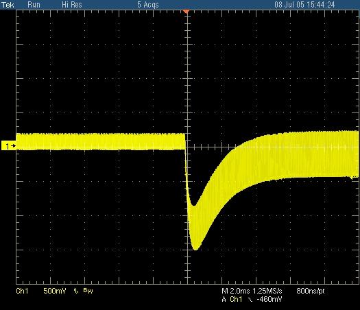
5 Static Measurements Soft Start CS CS Drain Drain At 30 Vac, full load At 110 Vac, no load CS CS Drain Drain At 30 Vac, no load At 110 Vac, no load 5


6 Valley Switching At 30 Vac, full load At 110 Vac, full load Load Transients At 30 Vac, half load At 110 Vac, half load At 30 Vac, 0% to 0% load on 135 V output At 110 Vac, 0% to 0% load on 135 V output


7 Standby Vcc Vcc Standby burst at 110 Vac Vcc Vcc Transitions Between Modes Standby burst at 30 Vac 5V Standby 5V Standby 135V output 135V output Normal to Standby Transition Standby to Normal Transition 7
8 Board Layout 0V 1V V 5V 135V AC input Standby switch: Left: normal mode Right: standby mode Bill of Material IC1 IC IC3 IC4 X1 M1 Q1 T1 L1 F1 D1 D5, D10, D14, D1, D141 D D7 D11, D1, D111 D13 DZ DZ3 R1, R35 R Rbo Rbo1 Rbo Rhyst R3 R4 R5, R1 Rs1, Rs R NCP1337 TL431 SFH15A MC7L05 IRFIBN0A BS10 BC547 TDK SRW4/15EC X1V017, CLICK BCK OREGA RM4 A 50V KBU4K 1N4007 1N4937 1N414 MUR40 MUR40 3V9 V 1k 47k W.7Meg 1.Meg 15k k 0.15.k R7 R R10 R11 R1 R13, R1 R17 R1, R31 R19 R33,R34 P1 C1, C C3 C4 C5 C7 C C9 C10 C11, C13, C15, C5, C131 C1 C14, C1, C141 C17 C1 C0 C1 C3 C 10Meg 4kV k 10k 5.k 100k 1k 1.5k 47k 1k 330p 300Vac X 10p kv 0u 450V 1u 3V 10n 30V 33u 5V 100n 330p 1.5kV 1000u 35V 100u 5V 1000u 1V 100u 00V 1n.n Y1 470n

9 9 Board Picture Appendix Schematic A C10 Rs1 Rbo Rbo1 D7 R3 D R C D13 C0 D1 R R1 R11 C5 D111 C7 DZ C1 135V V 0V IC C141 IC1 X1 C131 C15 Rs C19 C9 IC3x IC3 R1 D10 R4 C3 R7 R10 P1 T1 0V C11 C1 R19 C5 mains F1 D5 L1 C1 C D1 R31 Rhyst R R1 R17 C3 R5 C1 D11 1V C14 C13 IN OUT ADJUST IC4 5Vstby C17 Reg 5V Out1V OutV Out1V OutV C Rbo
10 Appendix Schematic B C19 D13 R17 135V 1 11 C0 R33 0V D5 D1 C L1 C5 C7 R1 Rbo Rbo1 Rhyst Rbo C4 R31 IC IC1 R3 C11 R C T1 C9 D7 D DZ1 C10 C D111 C131 D11 C13 D1 C15 D141 D14 M1 R35 C141 Out1V C C14 OutV D1 C1 DZ R34 DZ3 C1 R10 R11 IN Out1V OutV IC4 Reg 5V ADJUST OUT C17 0V 1V V 5Vstby C1 F1 mains R X1 R4 R5 Rs Rs1 C1 D10 R7 C3 R IC3x R19 R1 C5 C1 IC R1 P1 R1 Q1 SW1 R13 R1 ON Semiconductor and are registered trademarks of Semiconductor Components Industries, LLC (SCILLC). SCILLC reserves the right to make changes without further notice to any products herein. SCILLC makes no warranty, representation or guarantee regarding the suitability of its products for any particular purpose, nor does SCILLC assume any liability arising out of the application or use of any product or circuit, and specifically disclaims any and all liability, including without limitation special, consequential or incidental damages. Typical parameters which may be provided in SCILLC data sheets and/or specifications can and do vary in different applications and actual performance may vary over time. All operating parameters, including Typicals must be validated for each customer application by customer s technical experts. SCILLC does not convey any license under its patent rights nor the rights of others. SCILLC products are not designed, intended, or authorized for use as components in systems intended for surgical implant into the body, or other applications intended to support or sustain life, or for any other application in which the failure of the SCILLC product could create a situation where personal injury or death may occur. Should Buyer purchase or use SCILLC products for any such unintended or unauthorized application, Buyer shall indemnify and hold SCILLC and its officers, employees, subsidiaries, affiliates, and distributors harmless against all claims, costs, damages, and expenses, and reasonable attorney fees arising out of, directly or indirectly, any claim of personal injury or death associated with such unintended or unauthorized use, even if such claim alleges that SCILLC was negligent regarding the design or manufacture of the part. SCILLC is an Equal Opportunity/Affirmative Action Employer. This literature is subject to all applicable copyright laws and is not for resale in any manner. PUBLICATION ORDERING INFORMATION LITERATURE FULFILLMENT: Literature Distribution Center for ON Semiconductor P.O. Box 131, Phoenix, Arizona USA Phone: or Toll Free USA/Canada Fax: or Toll Free USA/Canada orderlit@onsemi.com N. American Technical Support: Toll Free USA/Canada Japan: ON Semiconductor, Japan Customer Focus Center 9 1 Kamimeguro, Meguro ku, Tokyo, Japan Phone: ON Semiconductor Website: Order Literature: For additional information, please contact your local Sales Representative. AND4/D
1. DEFINE THE SPECIFICATION 2. SELECT A TOPOLOGY
 How to Choose for Design This article is to present a way to choose a switching controller for design in the s Selector Guide SGD514/D from ON Semiconductor. (http://www.onsemi.com/pub/collateral/sgd514d.pdf)
NUP4302MR6T1G. Schottky Diode Array for Four Data Line ESD Protection
 Schottky Diode Array for Four Data Line ESD Protection The NUP432MR6 is designed to protect high speed data line interface from ESD, EFT and lighting. Features Very Low Forward Voltage Drop Fast Switching
Low Capacitance Transient Voltage Suppressors / ESD Protectors CM QG/D. Features
 Low Capacitance Transient Voltage Suppressors / ESD Protectors CM1250-04QG Features Low I/O capacitance at 5pF at 0V In-system ESD protection to ±8kV contact discharge, per the IEC 61000-4-2 international
NCP5425DEMO/D. NCP5425 Demonstration Board Note. Single Input to Dual Output Buck Regulator 5.0 V to 1.5 V/15 A and 1.8 V/15 A DEMONSTRATION NOTE
 NCP5425 Demonstration Board Note Single Input to Dual Output Buck Regulator 5.0 V to 1.5 V/15 A and 1.8 V/15 A DEMONSTRATION NOTE Description The NCP5425 demonstration board is a 4.0 by 4.0, two layer
AND8285/D. NCP1521B Adjustable Output Voltage Step Down Converter Simulation Procedure SIMULATION NOTE
 NCP1521B Adjustable Output Voltage Step Down Converter Simulation Procedure Prepared by: Bertrand Renaud On Semiconductor SIMULATION NOTE Overview The NCP1521B step down PWM DC DC converter is optimized
AND9043/D. An Off-Line, Power Factor Corrected, Buck-Boost Converter for Low Power LED Applications APPLICATION NOTE.
 An Off-Line, Power Factor Corrected, Buck-Boost Converter for Low Power LED Applications Prepared by: Frank Cathell ON Semiconductor Introduction This application note introduces a universal input, off
NCP1207AADAPGEVB. Implementing NCP1207 in QR 24 W AC-DC Converter with Synchronous Rectifier Evaluation Board User's Manual EVAL BOARD USER S MANUAL
 NCP07AADAPGEVB Implementing NCP07 in QR 4 W AC-DC Converter with Synchronous Rectifier Evaluation Board User's Manual EVAL BOARD USER S MANUAL Introduction The NCP07 is a controller dedicated for driving
AND8312/D. A 36W Ballast Application with the NCP5104
 A 6W Ballast Application with the P50 Prepared by: Thierry Sutto This document describes how the P50 driver can be implemented in a ballast application. The scope of this application note is to highlight
60 W Adapter Documentation Package Evaluation Board User's Manual
 60 W Adapter Documentation Package Evaluation Board User's Manual EVAL BOARD USER S MANUAL Overview This reference document describes a built-and-tested, GreenPoint solution for a 60 W power adapter. The
 Distributed by: www.jameco.com 1-800-831-4242 The content and copyrights of the attached material are the property of its owner. Preferred Device Small Signal MOSFET 500 ma, 60 Volts N Channel Features
AND8291/D. >85% Efficient 12 to 5 VDC Buck Converter
 >5% Efficient to 5 VDC Buck Converter Prepared by: DENNIS SOLLEY ON Semiconductor General Description This application note describes how the NCP363 can be configured as a buck controller to drive an external
NTS2101P. Power MOSFET. 8.0 V, 1.4 A, Single P Channel, SC 70
 NTS11P Power MOSFET 8. V, 1.4 A, Single P Channel, SC 7 Features Leading Trench Technology for Low R DS(on) Extending Battery Life 1.8 V Rated for Low Voltage Gate Drive SC 7 Surface Mount for Small Footprint
NTD7N ELECTRICAL CHARACTERISTICS ( unless otherwise stated) Parameter Symbol Test Condition Min Typ Max Unit OFF CHARACTERISTICS Drain to Source Break
 Parameter Symbol Test Condition Min Typ Max Unit OFF CHARACTERISTICS Drain to Source Break") NTD7N Power MOSFET V, 8 A, Single N Channel, Features Low R DS(on) High Current Capability Low Gate Charge These are Pb Free Devices Applications Electronic Brake Systems Electronic Power Steering Bridge
NTD7N Power MOSFET V, 8 A, Single N Channel, Features Low R DS(on) High Current Capability Low Gate Charge These are Pb Free Devices Applications Electronic Brake Systems Electronic Power Steering Bridge
NTF2955. Power MOSFET. 60 V, 2.6 A, Single P Channel SOT 223
 NTF955 Power MOSFET V,. A, Single P Channel SOT Features TMOS7 Design for low R DS(on) Withstands High Energy in Avalanche and Commutation Modes Pb Free Package is Available Applications Power Supplies
AND8295/D. A 36W Ballast Application with the NCP5106B
 A 36W Ballast Application with the NCP506B Prepared by: Thierry Sutto This document describes how the NCP506B driver can be implemented in a ballast application. The scope of this application note is to
MPS5172G. General Purpose Transistor. NPN Silicon. Pb Free Packages are Available* Features. MAXIMUM RATINGS THERMAL CHARACTERISTICS
 General Purpose Transistor NPN Silicon Features Pb Free Packages are Available* MAXIMUM RATINGS Rating Symbol Value Unit Collector Emitter Voltage V CEO 25 Vdc Collector Base Voltage V CBO 25 Vdc Emitter
PIN CONNECTIONS
 The NCP4421/4422 are high current buffer/drivers capable of driving large MOSFETs and IGBTs. They are essentially immune to any form of upset except direct overvoltage or over dissipation they cannot be
DEMONSTRATION NOTE. Figure 1. CS51411/3 Demonstration Board. 1 Publication Order Number: CS51411DEMO/D
 DEMONSTRATION NOTE Description The CS51411 demonstration board is a 1.0 A/3.3 V buck regulator running at 260 khz (CS51411) or 520 khz (CS51413). The switching frequency can be synchronized to a higher
AND8136/D. Offline LED Driver APPLICATION NOTE. Input Peak Current:
 Offline LED Driver APPLICATION NOTE This application note provides a simple approach to designing an LED driver utilizing the ON Semiconductor NCP1014 self supplied monolithic switcher. The easy to follow,
NTNUS3171PZ. Small Signal MOSFET. 20 V, 200 ma, Single P Channel, 1.0 x 0.6 mm SOT 1123 Package
 NTNUS7PZ Small Signal MOSFET V, ma, Single P Channel,. x.6 mm SOT Package Features Single P Channel MOSFET Offers a Low R DS(on) Solution in the Ultra Small. x.6 mm Package. V Gate Voltage Rating Ultra
NTMD4184PFR2G. Power MOSFET and Schottky Diode -30 V, -4.0 A, Single P-Channel with 20 V, 2.2 A, Schottky Barrier Diode Features
 NTMDPF Power MOSFET and Schottky Diode -3 V, -. A, Single P-Channel with V,. A, Schottky Barrier Diode Features FETKY Surface Mount Package Saves Board Space Independent Pin-Out for MOSFET and Schottky
NTLJD4116NT1G. Power MOSFET. 30 V, 4.6 A, Cool Dual N Channel, 2x2 mm WDFN Package
 NTLJDN Power MOSFET V,. A, Cool Dual N Channel, x mm WDFN Package Features WDFN Package Provides Exposed Drain Pad for Excellent Thermal Conduction x mm Footprint Same as SC 88 Lowest R DS(on) Solution
MBRB20200CT. SWITCHMODE Power Rectifier. Dual Schottky Rectifier SCHOTTKY BARRIER RECTIFIER 20 AMPERES, 200 V
 MBRBCT SWITCHMODE Power Rectifier Dual Schottky Rectifier This device uses the Schottky Barrier technology with a platinum barrier metal. This state of the art device is designed for use in high frequency
NSTB1005DXV5T1, NSTB1005DXV5T5. Dual Common Base Collector Bias Resistor Transistors
 NSTB005DXV5T, NSTB005DXV5T5 Preferred Devices Dual Common Base Collector Bias Resistor Transistors NPN and PNP Silicon Surface Mount Transistors with Monolithic Bias Resistor Network The BRT (Bias Resistor
MPSA20. Amplifier Transistor. NPN Silicon. Pb Free Package is Available* Features. MAXIMUM RATINGS THERMAL CHARACTERISTICS
 MPSA Amplifier Transistor NPN Silicon Features Pb Free Package is Available* MAXIMUM RATINGS Rating Symbol Value Unit Collector Emitter Voltage V CEO 4 Vdc Collector Base Voltage V CBO 4. Vdc Collector
Is Now Part of To learn more about ON Semiconductor, please visit our website at
 Is Now Part of To learn more about ON Semiconductor, please visit our website at www.onsemi.com ON Semiconductor and the ON Semiconductor logo are trademarks of Semiconductor Components Industries, LLC
NTMD4820NR2G. Power MOSFET 30 V, 8 A, Dual N Channel, SOIC 8
 NTMDN Power MOSFET V, A, Dual N Channel, SOIC Features Low R DS(on) to Minimize Conduction Losses Low Capacitance to Minimize Driver Losses Optimized Gate Charge to Minimize Switching Losses Dual SOIC
NCP800. Lithium Battery Protection Circuit for One Cell Battery Packs
 Lithium Battery Protection Circuit for One Cell Battery Packs The NCP800 resides in a lithium battery pack where the battery cell continuously powers it. In order to maintain cell operation within specified
CS PIN CONNECTIONS AND MARKING DIAGRAM ORDERING INFORMATION SO 14 D SUFFIX CASE 751A V CC. = Assembly Location
 The CS3361 integral alternator regulator integrated circuit provides the voltage regulation for automotive, 3 phase alternators. It drives an external logic level N channel enhancement power FET for control
BS107, BS107A. Small Signal MOSFET 250 mamps, 200 Volts N Channel TO ma, 200 V R DS(on) = 14 (BS107) R DS(on) = 6.
 = 14 (BS107) R DS(on) = 6.") Preferred Device Small Signal MOSFET 250 mamps, 200 Volts NChannel Features PbFree Package is Available* 250 ma, 200 V R DS(on) = 14 (BS107) R DS(on) = 6.4 (BS107A) MAXIMUM RATINGS Rating Symbol Value
Preferred Device Small Signal MOSFET 250 mamps, 200 Volts NChannel Features PbFree Package is Available* 250 ma, 200 V R DS(on) = 14 (BS107) R DS(on) = 6.4 (BS107A) MAXIMUM RATINGS Rating Symbol Value
NCL30000LED2GEVB/D Vac up to 15 Watt Dimmable LED Driver Demo Board Operation EVALUATION BOARD MANUAL
 180-265 Vac up to 15 Watt Dimmable LED Driver Demo Board Operation Prepared by: Jim Young ON Semiconductor EVALUATION BOARD MANUAL Introduction The NCL30000 is a power factor corrected LED driver controller.
AND9006/D. Using Transmission Line Pulse Measurements to Understand Protection Product Characteristics APPLICATION NOTE
 Using Transmission Line Pulse Measurements to Understand Protection Product Characteristics Prepared by: Robert Ashton ON Semiconductor APPLICATION NOTE INTRODUCTION Transmission Line Pulse (TLP) is a
MPSA70. Amplifier Transistor. PNP Silicon. Pb Free Package is Available* Features. MAXIMUM RATINGS THERMAL CHARACTERISTICS
 Amplifier Transistor PNP Silicon Features Pb Free Package is Available* MAXIMUM RATINGS Rating Symbol Value Unit Collector Emitter Voltage V CEO 4 Vdc Emitter Base Voltage V EBO 4. Vdc Collector Current
NTMD4840NR2G. Power MOSFET 30 V, 7.5 A, Dual N Channel, SOIC 8
 NTMDN Power MOSFET 3 V, 7. A, Dual N Channel, SOIC Features Low R DS(on) to Minimize Conduction Losses Low Capacitance to Minimize Driver Losses Optimized Gate Charge to Minimize Switching Losses Dual
AND8450/D. NCV7680 LED Driver Linear Regulator Performance APPLICATION NOTE
 NCV7680 LED Driver Linear Regulator Performance APPLICATION NOTE Introduction The NCV7680 is an automotive LED driver targeted primarily for rear combination lamp systems. A high input voltage to this
MR2520LRL. Overvoltage Transient Suppressor OVERVOLTAGE TRANSIENT SUPPRESSOR VOLTS
 Overvoltage Transient Suppressor Designed for applications requiring a low voltage rectifier with reverse avalanche characteristics for use as reverse power transient suppressors. Developed to suppress
NTGD4167C. Power MOSFET Complementary, 30 V, +2.9/ 2.2 A, TSOP 6 Dual
 Power MOSFET Complementary, 3 V, +.9/. A, TSOP 6 Dual Features Complementary N Channel and P Channel MOSFET Small Size (3 x 3 mm) Dual TSOP 6 Package Leading Edge Trench Technology for Low On Resistance
AND9100/D. Paralleling of IGBTs APPLICATION NOTE. Isothermal point
 Paralleling of IGBTs Introduction High power systems require the paralleling of IGBTs to handle loads well into the 10 s and sometimes the 100 s of kilowatts. Paralleled devices can be discrete packaged
NTS4173PT1G. Power MOSFET. 30 V, 1.3 A, Single P Channel, SC 70
 NTS17P Power MOSFET V, 1. A, Single P Channel, SC 7 Features V BV ds, Low R DS(on) in SC 7 Package Low Threshold Voltage Fast Switching Speed This is a Halide Free Device This is a Pb Free Device Applications
MMSZ4678ET1 Series. Zener Voltage Regulators. 500 mw SOD 123 Surface Mount
 MMSZ4678ET Series Zener Voltage Regulators 5 mw SOD 3 Surface Mount Three complete series of Zener diodes are offered in the convenient, surface mount plastic SOD 3 package. These devices provide a convenient
The MC10109 is a dual 4 5 input OR/NOR gate. P D = 30 mw typ/gate (No Load) t pd = 2.0 ns typ t r, t f = 2.0 ns typ (20% 80%)
 t pd = 2.0 ns typ t r, t f = 2.0 ns typ (20% 80%)") The MC10109 is a dual 5 input OR/NOR gate. P D = 0 mw typ/gate (No Load) t pd =.0 ns typ t r, t f =.0 ns typ (0% 0%) LOGIC DIAGRAM MARKING DIAGRAMS CDIP 16 L SUFFIX CASE 60 PDIP 16 P SUFFIX CASE 6 PLCC
The MC10109 is a dual 5 input OR/NOR gate. P D = 0 mw typ/gate (No Load) t pd =.0 ns typ t r, t f =.0 ns typ (0% 0%) LOGIC DIAGRAM MARKING DIAGRAMS CDIP 16 L SUFFIX CASE 60 PDIP 16 P SUFFIX CASE 6 PLCC
NTS4172NT1G. Power MOSFET. 30 V, 1.7 A, Single N Channel, SC 70. Low On Resistance Low Gate Threshold Voltage Halide Free This is a Pb Free Device
 Power MOSFET V,.7 A, Single N Channel, SC 7 Features Low On Resistance Low Gate Threshold Voltage Halide Free This is a Pb Free Device V (BR)DSS R DS(on) MAX I D MAX Applications Low Side Load Switch DC
MMBFU310LT1G. JFET Transistor. N Channel. These Devices are Pb Free, Halogen Free/BFR Free and are RoHS Compliant. Features.
 MMBFULT1G JFET Transistor N Channel Features These Devices are Pb Free, Halogen Free/BFR Free and are RoHS Compliant 2 SOURCE MAXIMUM RATINGS Rating Symbol Value Unit Drain Source Voltage V DS 25 Vdc Gate
NVLJD4007NZTBG. Small Signal MOSFET. 30 V, 245 ma, Dual, N Channel, Gate ESD Protection, 2x2 WDFN Package
 NVLJD7NZ Small Signal MOSFET V, 2 ma, Dual, N Channel, Gate ESD Protection, 2x2 WDFN Package Features Optimized Layout for Excellent High Speed Signal Integrity Low Gate Charge for Fast Switching Small
MMSZ2V4T1 Series. Zener Voltage Regulators. 500 mw SOD 123 Surface Mount
 MMSZVT Series Zener Voltage Regulators 5 mw SOD 3 Surface Mount Three complete series of Zener diodes are offered in the convenient, surface mount plastic SOD 3 package. These devices provide a convenient
AND8125/D. Evaluating the Power Capability of NCP101X Members APPLICATION NOTE
 Evaluating the Power Capability of NCP101X Members Prepared by: Christophe Basso ON Semiconductor APPLICATION NOTE The NCP101X series is available in various combinations of peak current and switching
NTGS3441BT1G. Power MOSFET. -20 V, -3.5 A, Single P-Channel, TSOP-6. Low R DS(on) in TSOP-6 Package 2.5 V Gate Rating This is a Pb-Free Device
 in TSOP-6 Package 2.5 V Gate Rating This is a Pb-Free Device") Power MOSFET - V, -. A, Single P-Channel, TSOP- Features Low R DS(on) in TSOP- Package. V Gate Rating This is a Pb-Free Device Applications Battery Switch and Load Management Applications in Portable Equipment
Power MOSFET - V, -. A, Single P-Channel, TSOP- Features Low R DS(on) in TSOP- Package. V Gate Rating This is a Pb-Free Device Applications Battery Switch and Load Management Applications in Portable Equipment
MJW0281A (NPN) MJW0302A (PNP) Complementary NPN PNP Power Bipolar Transistors 15 AMPERES COMPLEMENTARY SILICON POWER TRANSISTORS 260 VOLTS 150 WATTS
 MJW0302A (PNP) Complementary NPN PNP Power Bipolar Transistors 15 AMPERES COMPLEMENTARY SILICON POWER TRANSISTORS 260 VOLTS 150 WATTS") MJW28A (NPN) MJW32A (PNP) Preferred Devices Complementary NPN PNP Power Bipolar Transistors These complementary devices are lower power versions of the popular MJW328A and MJW32A audio output transistors.
MJW28A (NPN) MJW32A (PNP) Preferred Devices Complementary NPN PNP Power Bipolar Transistors These complementary devices are lower power versions of the popular MJW328A and MJW32A audio output transistors.
EMF5XV6T5G. Power Management, Dual Transistors. NPN Silicon Surface Mount Transistors with Monolithic Bias Resistor Network
 Preferred Devices Power Management, Dual Transistors NPN Silicon Surface Mount Transistors with Monolithic Bias Resistor Network Features Simplifies Circuit Design Reduces Board Space Reduces Component
NSR0340V2T1/D. Schottky Barrier Diode 40 VOLT SCHOTTKY BARRIER DIODE
 Schottky Barrier Diode Schottky barrier diodes are optimized for very low forward voltage drop and low leakage current and are used in a wide range of dc dc converter, clamping and protection applications
MUR8100E, MUR880E. SWITCHMODE Power Rectifiers. Ultrafast E Series with High Reverse Energy Capability ULTRAFAST RECTIFIERS 8.
 MUR8E, MUR88E MUR8E is a Preferred Device SWITCHMODE Power Rectifiers Ultrafast E Series with High Reverse Energy Capability The MUR8 and MUR88E diodes are designed for use in switching power supplies,
NUP2105LT3G. Dual Line CAN Bus Protector SOT 23 DUAL BIDIRECTIONAL VOLTAGE SUPPRESSOR 350 W PEAK POWER
 Dual Line CAN Bus Protector The NUP2105L has been designed to protect the CAN transceiver in high speed and fault tolerant networks from ESD and other harmful transient voltage events. This device provides
DUAL TIMING CIRCUIT SEMICONDUCTOR TECHNICAL DATA PIN CONNECTIONS ORDERING INFORMATION. Figure Second Solid State Time Delay Relay Circuit
 The MC3456 dual timing circuit is a highly stable controller capable of producing accurate time delays, or oscillation. Additional terminals are provided for triggering or resetting if desired. In the
NJL3281D (NPN) NJL1302D (PNP) Complementary ThermalTrak Transistors BIPOLAR POWER TRANSISTORS 15 A, 260 V, 200 W
 NJL1302D (PNP) Complementary ThermalTrak Transistors BIPOLAR POWER TRANSISTORS 15 A, 260 V, 200 W") NJL3281D (NPN) NJL132D (PNP) Complementary ThermalTrak Transistors The ThermalTrak family of devices has been designed to eliminate thermal equilibrium lag time and bias trimming in audio amplifier applications.
NJL3281D (NPN) NJL132D (PNP) Complementary ThermalTrak Transistors The ThermalTrak family of devices has been designed to eliminate thermal equilibrium lag time and bias trimming in audio amplifier applications.
AND8289. LED Driving with NCP/V3063
 LE riving with NCP/V3063 Prepared by: Petr Konvicny, Bernie Weir ON Semiconductor Introduction Improvements in high brightness LEs present the potential for creative new lighting solutions that offer an
CMPWR ma SmartOR Regulator with V AUX Switch
 50 ma SmartOR Regulator with Switch Product Description The ON Semiconductor s SmartOR is a low dropout regulator that delivers up to 50 ma of load current at a fixed 3.3 V output. An internal threshold
NCP1216AFORWGEVB. Implementing a DC/DC Single ended Forward Converter with the NCP1216A Evaluation Board User's Manual EVAL BOARD USER S MANUAL
 Implementing a DC/DC Single ended Forward Converter with the NCP1216A Evaluation Board User's Manual Introduction This document describes how the NCP1216A controller can be used to design a DC/DC single-ended
NTA4001N, NVA4001N. Small Signal MOSFET. 20 V, 238 ma, Single, N Channel, Gate ESD Protection, SC 75
 Small Signal MOSFET V, 8 ma, Single, N Channel, Gate ESD Protection, SC 75 Features Low Gate Charge for Fast Switching Small.6 x.6 mm Footprint ESD Protected Gate AEC Q Qualified and PPAP Capable NVA4N
MBRD835LT4G. SWITCHMODE Power Rectifier. DPAK Surface Mount Package SCHOTTKY BARRIER RECTIFIER 8.0 AMPERES, 35 VOLTS
 MBRD8L Preferred Device SWITCHMODE Power Rectifier Surface Mount Package This SWITCHMODE power rectifier which uses the Schottky Barrier principle with a proprietary barrier metal, is designed for use
BC517G. Darlington Transistors. NPN Silicon. Pb Free Packages are Available* Features. MAXIMUM RATINGS THERMAL CHARACTERISTICS
 Darlington Transistors NPN Silicon Features Pb Free Packages are Available* COLLECTOR 1 MAXIMUM RATINGS Rating Symbol Value Unit Collector Emitter Voltage V CES 30 Collector Base Voltage V CB 40 Collector
NCP1631EVB/D. NCP1631 Evaluation Board Manual. Performance of a 300 W, Wide Mains Interleaved PFC Driven by the NCP1631 EVALUATION BOARD MANUAL
 P1631EVB/D P1631 Evaluation Board Manual Performance of a 300 W, Wide Mains Interleaved PFC Driven by the P1631 Prepared by: Stephanie Conseil ON Semiconductor EVALUATION BOARD MANUAL The P1631 is a dual
AND8161/D. Implementing a DC/DC Single Ended Forward Converter with the NCP1216A APPLICATION NOTE
 Implementing a DC/DC Single Ended Forward Converter with the NCP1216A Prepared by: Roman Stuler APPLICATION NOTE This document describes how the NCP 1216A controller can be used to design a DC/DC single
EVALUATION BOARD FOR STK N, 120N, 140N. Phenol 1-layer Board) Figure 2. STK NGEVB Figure 3. STK NGEVB Figure 4.
 Figure 2. STK NGEVB Figure 3. STK NGEVB Figure 4.") STK44-NGEVB, STK44-1NGEVB, STK44-14NGEVB STK44-N Series Evaluation Board User's Manual EVAL BOARD USER S MANUAL Thick-Film Hybrid IC for use used in from 6 W to 18 W 1ch class AB audio power amplifiers.
STK44-NGEVB, STK44-1NGEVB, STK44-14NGEVB STK44-N Series Evaluation Board User's Manual EVAL BOARD USER S MANUAL Thick-Film Hybrid IC for use used in from 6 W to 18 W 1ch class AB audio power amplifiers.
NTNS3164NZT5G. Small Signal MOSFET. 20 V, 361 ma, Single N Channel, SOT 883 (XDFN3) 1.0 x 0.6 x 0.4 mm Package
 1.0 x 0.6 x 0.4 mm Package") NTNS36NZ Small Signal MOSFET V, 36 ma, Single N Channel, SOT 883 (XDFN3). x.6 x. mm Package Features Single N Channel MOSFET Ultra Low Profile SOT 883 (XDFN3). x.6 x. mm for Extremely Thin Environments
NTNS36NZ Small Signal MOSFET V, 36 ma, Single N Channel, SOT 883 (XDFN3). x.6 x. mm Package Features Single N Channel MOSFET Ultra Low Profile SOT 883 (XDFN3). x.6 x. mm for Extremely Thin Environments
NTK3139P. Power MOSFET. 20 V, 780 ma, Single P Channel with ESD Protection, SOT 723
 NTK9P Power MOSFET V, 78 ma, Single P Channel with ESD Protection, SOT 7 Features P channel Switch with Low R DS(on) % Smaller Footprint and 8% Thinner than SC 89 Low Threshold Levels Allowing.5 V R DS(on)
MMBT3906LT3G. PNP Silicon. Pb-Free Packages are Available. Features. MAXIMUM RATINGS THERMAL CHARACTERISTICS MARKING DIAGRAM
 Preferred Device General Purpose Transistor PNP Silicon Features PbFree Packages are Available MAXIMUM RATINGS Rating Symbol Value Unit Collector Emitter Voltage V CEO 4 Collector Base Voltage V CBO 4
Extended V GSS range ( 25V) for battery applications
 for battery applications") Dual Volt P-Channel PowerTrench MOSFET General Description This P-Channel MOSFET has been designed specifically to improve the overall efficiency of DC/DC converters using either synchronous or conventional
Dual Volt P-Channel PowerTrench MOSFET General Description This P-Channel MOSFET has been designed specifically to improve the overall efficiency of DC/DC converters using either synchronous or conventional
AND8142/D. A 6.0 W/12 W Universal Mains Adapter with the NCP101X APPLICATION NOTE
 A 6.0 W/12 W Universal Mains Adapter with the NCP101X Prepared by: Christophe Basso ON Semiconductor APPLICATION NOTE The present report depicts a demonstration board built around the NCP1013P06, a new
MARKING DIAGRAMS LOGIC DIAGRAM ORDERING INFORMATION DIP PIN ASSIGNMENT CDIP 16 L SUFFIX CASE 620 MC10124L AWLYYWW
 The MC024 is a quad translator for interfacing data and control signals between a saturated logic section and the MECL section of digital systems. The MC024 has TTL compatible inputs, and MECL complementary
BAT54CLT3G SBAT54CLT1G. Dual Common Cathode Schottky Barrier Diodes 30 VOLT DUAL COMMON CATHODE SCHOTTKY BARRIER DIODES
 BAT54CLTG, SBAT54CLTG Dual Common Cathode Schottky Barrier Diodes These Schottky barrier diodes are designed for high speed switching applications, circuit protection, and voltage clamping. Extremely low
NCP5504, NCV ma Dual Output Low Dropout Linear Regulator
 25 ma Dual Output Low Dropout Linear Regulator The NCP554/NCV554 are dual output low dropout linear regulators with 2.% accuracy over the operating temperature range. They feature a fixed output voltage
P SUFFIX CASE 646 Single Supply Split Supplies SO-14 D SUFFIX CASE 751A PIN CONNECTIONS
 Dual Operational Amplifier and Dual Comparator The MC05 contains two differential-input operational amplifiers and two comparators, each set capable of single supply operation. This operational amplifier-comparator
MPSL51. Amplifier Transistor PNP Silicon MAXIMUM RATINGS. THERMAL CHARACTERISTICS
 Amplifier Transistor PNP Silicon MAXIMUM RATINGS Rating Symbol alue Unit Collector Emitter oltage CEO dc Collector Base oltage CBO dc Emitter Base oltage EBO 4. dc Collector Current Continuous I C 6 madc
NDF10N62Z. N-Channel Power MOSFET
 NDFNZ N-Channel Power MOSFET V,.7 Features Low ON Resistance Low Gate Charge ESD Diode Protected Gate % Avalanche Tested These Devices are Pb Free, Halogen Free/BFR Free and are RoHS Compliant V DSS R
NSQA6V8AW5T2 Series Transient Voltage Suppressor
 Transient Voltage Suppressor ESD Protection Diode with Low Clamping Voltage This integrated transient voltage suppressor device (TVS) is designed for applications requiring transient overvoltage protection.
MMBZ15VDLT3G MMBZ27VCLT1G SZMMBZ15VDLT3G. SZMMBZ27VCLT1G 40 Watt Peak Power Zener Transient Voltage Suppressors
 MMBZ15VDLT1G, MMBZ27VCLT1G, SZMMBZ15VDLT1G, SZMMBZ27VCLT1G 40 Watt Peak Power Zener Transient Voltage Suppressors Dual Common Cathode Zeners for ESD Protection These dual monolithic silicon zener diodes
General Description. Applications. Power management Load switch Q2 3 5 Q1
 FDG6342L Integrated Load Switch Features Max r DS(on) = 150mΩ at V GS = 4.5V, I D = 1.5A Max r DS(on) = 195mΩ at V GS = 2.5V, I D = 1.3A Max r DS(on) = 280mΩ at V GS = 1.8V, I D = 1.1A Max r DS(on) = 480mΩ
NCP786L. Wide Input Voltage Range 5 ma Ultra-Low Iq, High PSRR Linear Regulator with Adjustable Output Voltage
 Wide Input Voltage Range 5 ma Ultra-Low Iq, High PSRR Linear Regulator with Adjustable Output Voltage The is high performance linear regulator, offering a very wide operating input voltage range of up
MC10H352. Quad CMOS to PECL* Translator
 Quad CMOS to PECL* Translator Description The MC10H352 is a quad translator for interfacing data between a CMOS logic section and the PECL section of digital systems when only a +5.0 Vdc power supply is
MMSD301T1G SMMSD301T1G, MMSD701T1G SMMSD701T1G, SOD-123 Schottky Barrier Diodes
 MMSD3TG, SMMSD3TG, MMSD7TG, SMMSD7TG, SOD-3 Schottky Barrier Diodes The MMSD3T, and MMSD7T devices are spinoffs of our popular MMBD3LT, and MMBD7LT SOT3 devices. They are designed for highefficiency UHF
NTHD2102PT1G. Power MOSFET. 8.0 V, 4.6 A Dual P Channel ChipFET
 NTHDP Power MOSFET. V,. A Dual PChannel ChipFET Features Offers an Ultra Low R DS(on) Solution in the ChipFET Package Miniature ChipFET Package % Smaller Footprint than TSOP making it an Ideal Device for
74VHC14 Hex Schmitt Inverter
 74HC14 Hex Schmitt Inverter Features High Speed: t PD = 5.5 ns (Typ.) at CC = 5 Low Power Dissipation: I CC = 2 μa (Max.) at T A = 25 C High Noise Immunity: NIH = NIL = 28% CC (Min.) Power down protection
MARKING DIAGRAMS LOGIC DIAGRAM ORDERING INFORMATION DIP PIN ASSIGNMENT CDIP 16 L SUFFIX CASE 620 MC10216L AWLYYWW
 The MC1016 is a high speed triple differential amplifier designed for use in sensing differential signals over long lines. The base bias supply (V BB ) is made available at pin 11 to make the device useful
BDW42 NPN, BDW46, BDW47 PNP. Darlington Complementary Silicon Power Transistors
 BDW42 NPN,, BDW47 PNP BDW42 and BDW47 are Preferred Devices Darlington Complementary Silicon Power Transistors This series of plastic, medium power silicon NPN and PNP Darlington transistors are designed
MMSZ5221BT1 Series. Zener Voltage Regulators. 500 mw SOD 123 Surface Mount
 MMSZ5BT Series Preferred Device Zener Voltage Regulators 5 mw SOD 3 Surface Mount Three complete series of Zener diodes are offered in the convenient, surface mount plastic SOD 3 package. These devices
CAT4237EVAL2EVB. CAT4237 High Voltage White LED Driver Evaluation Board User's Manual EVAL BOARD USER S MANUAL
 CAT4237 High Voltage White LED Driver Evaluation Board User's Manual EVAL BOARD USER S MANUAL Introduction This document describes the CAT4237EVAL2 Evaluation Board for the Catalyst Semiconductor CAT4237
Overview The LA1225MC is a Low-voltage operation (1.8V or higher) FM IF detector IC for the electronic tuning system.
 FM IF detector IC for the electronic tuning system.") Ordering number : ENA2052 LA1225MC Monolithic Linear IC FM IF Detector IC http://onsemi.com Overview The LA1225MC is a Low-voltage operation (1.8V or higher) FM IF detector IC for the electronic tuning
Ordering number : ENA2052 LA1225MC Monolithic Linear IC FM IF Detector IC http://onsemi.com Overview The LA1225MC is a Low-voltage operation (1.8V or higher) FM IF detector IC for the electronic tuning
Single stage LNA for GPS Using the MCH4009 Application Note
 Single stage LNA for GPS Using the MCH49 Application Note http://onsemi.com Overview This application note explains about ON Semiconductor s MCH49 which is used as a Low Noise Amplifier (LNA) for GPS (Global
AND8179/D. Using Critical Conduction Mode for High Power Factor Correction APPLICATION NOTE
 Using Critical Conduction Mode for High Power Factor Correction Prepared by: Frank Cathell ON Semiconductor APPLICATION NOTE Introduction Power Factor Correction (PFC) is very much a necessity for off
MMBZ15VDLT3G MMBZ27VCLT1G. 40 Watt Peak Power Zener Transient Voltage Suppressors. SOT-23 Dual Common Cathode Zeners for ESD Protection
 MMBZ5VDLT, MMBZ7VCLT Preferred s 40 Watt Peak Power Zener Transient Voltage Suppressors SOT- Dual Common Cathode Zeners for ESD Protection These dual monolithic silicon zener diodes are designed for applications
BAV70DXV6T1, BAV70DXV6T5 Preferred Device. Monolithic Dual Switching Diode Common Cathode. Lead-Free Solder Plating.
 BAV70DXV6T1, BAV70DXV6T5 Preferred Device Monolithic Dual Switching Diode Common Cathode LeadFree Solder Plating MAXIMUM RATINGS (EACH DIODE) Rating Symbol Value Unit Reverse Voltage V R 70 Vdc Forward
J309, J310. N Channel Depletion. Pb Free Packages are Available* Features. MAXIMUM RATINGS MARKING DIAGRAM
 J39, Preferred Device JFET VHF/UHF Amplifiers NChannel Depletion Features PbFree Packages are Available* MAXIMUM RATINGS Rating Symbol Value Unit DrainSource Voltage V DS 25 Vdc Gate Source Voltage V GS
NCP A Low Dropout Linear Regulator
 1.5 A Low Dropout Linear Regulator The NCP566 low dropout linear regulator will provide 1.5 A at a fixed output voltage. The fast loop response and low dropout voltage make this regulator ideal for applications
NTTFS5820NLTWG. Power MOSFET. 60 V, 37 A, 11.5 m. Low R DS(on) Low Capacitance Optimized Gate Charge These Devices are Pb Free and are RoHS Compliant
 Low Capacitance Optimized Gate Charge These Devices are Pb Free and are RoHS Compliant") NTTFS582NL Power MOSFET 6 V, 37 A,.5 m Features Low R DS(on) Low Capacitance Optimized Gate Charge These Devices are Pb Free and are RoHS Compliant MAXIMUM RATINGS ( unless otherwise stated) Parameter
NTTFS582NL Power MOSFET 6 V, 37 A,.5 m Features Low R DS(on) Low Capacitance Optimized Gate Charge These Devices are Pb Free and are RoHS Compliant MAXIMUM RATINGS ( unless otherwise stated) Parameter
NTJS3151P. Trench Power MOSFET. 12 V, 3.3 A, Single P Channel, ESD Protected SC 88
 NTJS5P Trench Power MOSFET V,. A, Single P Channel, ES Protected SC 88 Features Leading Trench Technology for Low R S(ON) Extending Battery Life SC 88 Small Outline (x mm, SC7 Equivalent) Gate iodes for
MUN5211DW1T1 Series. NPN Silicon Surface Mount Transistors with Monolithic Bias Resistor Network
 MUNDWT Series Preferred Devices Dual Bias Resistor Transistors NPN Silicon Surface Mount Transistors with Monolithic Bias Resistor Network The BRT (Bias Resistor Transistor) contains a single transistor
LOW POWER SCHOTTKY. GUARANTEED OPERATING RANGES ORDERING INFORMATION
 The SN74LS298 is a Quad 2-Port Register. It is the logical equivalent of a quad 2-input multiplexer followed by a quad 4-bit edge-triggered register. A Common Select input selects between two 4-bit input
NTTFS5116PLTWG. Power MOSFET 60 V, 20 A, 52 m. Low R DS(on) Fast Switching These Devices are Pb Free and are RoHS Compliant
 Fast Switching These Devices are Pb Free and are RoHS Compliant") Power MOSFET 6 V, 2 A, 52 m Features Low R DS(on) Fast Switching These Devices are Pb Free and are RoHS Compliant Applications Load Switches DC Motor Control DC DC Conversion MAXIMUM RATINGS ( unless otherwise
Power MOSFET 6 V, 2 A, 52 m Features Low R DS(on) Fast Switching These Devices are Pb Free and are RoHS Compliant Applications Load Switches DC Motor Control DC DC Conversion MAXIMUM RATINGS ( unless otherwise
NUD4700. LED Shunt. Features. Typical Applications MARKING DIAGRAM PIN FUNCTION DESCRIPTION ORDERING INFORMATION.
 LED Shunt The is an electronic shunt which provides a current bypass in the case of a single LED going into open circuit. LEDs are by nature quite fragile when subjected to transients and surge conditions.
Is Now Part of To learn more about ON Semiconductor, please visit our website at
 Is Now Part of To learn more about ON Semiconductor, please visit our website at www.onsemi.com ON Semiconductor and the ON Semiconductor logo are trademarks of Semiconductor Components Industries, LLC