Basic Electronic Devices and Circuits EE 111 Electrical Engineering Majmaah University 2 nd Semester 1432/1433 H. Chapter 2. Diodes and Applications
|
|
|
- Kelley Stewart
- 6 years ago
- Views:
Transcription
1 Basic Electronic Devices and Circuits EE 111 Electrical Engineering Majmaah University 2 nd Semester 1432/1433 H Chapter 2 Diodes and Applications 1
2 Diodes A diode is a semiconductor device with a single pn junction and metal connections to leads. It has the ability to pass current in only one direction. p n Depletion region 2
3 Forward bias Forward bias is the condition which allows current in the diode. The bias voltage must be greater than the barrier potential. I F (ma) V F R I F VBIAS 0 0 A B C 0.7 V Knee V F 3
4 Quiz Q. The forward biased knee voltage in a semiconductor diode is approximately equal to the a. bias supply voltage b. breakdown voltage c. output voltage d. barrier potential 4
5 Reverse bias Reverse bias is the condition in which current is blocked. V BIAS V R V BR Knee 0 0 I = 0 A R V BIAS I R 5
6 Approximations Three diode approximations are: I F I F I F V R V F V R 0.7 V V F V R 0.7 V V F I R I R slope > 0 Ideal Practical Complete I R In addition, the complete model includes the effect of a large reverse resistance that accounts for a tiny current when reverse-biased. 6
7 1. Ideal Model 7
8 2. Practical Model 8
9 3. Complete Model 9
10 Example Use the practical model to determine the current in the circuit: R V BIAS 12 V 3.3 kω I VR = VBIAS 0.7 V= 12 V 0.7 V= 11.3 V I V R 11.3 V 3.3 kω R = = = 3.4 ma 10
11 Quiz Q. Using the ideal diode model, the current in the circuit shown is a ma R b ma c ma d. 1.2 ma V BIAS 8.0 V 10 kω 11
12 Quiz Q. Using the practical diode model, the current in the circuit shown is a ma R b ma c ma d. 1.2 ma V BIAS 8.0 V 10 kω 12
13 Quiz Q. The diode model which includes the large reverse resistance is the a. ideal model b. practical model c. complete model d. all of the above 13
14 Typical diode packages Some common configurations are K K A K A A A A K K K K A K A K K A K A K A 14
15 The Basic DC Power Supply 15
16 Half-wave Rectifier The diode conducts during the positive half cycle. It does not conduct during the negative half cycle. V in 0 t I R L 0 0 t1 2 t 0 t1 V out t t 2 I = 0 A V V out in 0 R t L 0 0 t1 t 2 t0 t1 t 2 What is the output if the diode is reversed? See next slide 16
17 Half-wave Rectifier V in 0 t I V out R L 0 0 t1 2 t 0 t1 t t 2 What is the output if the diode is reversed? 17

18 Average Value of the Half-Wave Output Voltage 18


19 Example 19
20 Effect of the Barrier Potential on the Half-Wave Rectifier Output 20
21 Half-wave Rectifier The peak inverse voltage (PIV) is equal to the peak input voltage and is the maximum voltage across the diode when it is not conducting. V 0 V p(in) t p PIV at t p I = 0 Notice that the PIV can be found by applying Kirchhoff s Voltage Law. The load voltage is 0 V, so the input voltage is across the diode at t p. R L 21
22 Full-Wave Rectification 22
23 Average Value of the Full-Wave Output Voltage 23
24 Full-wave Rectifier F D 1 A center-tapped transformer is used with two diodes that conduct on alternating halfcycles. V in 0 During the positive half-cycle, the upper diode is forward-biased and the lower diode is reverse-biased. V in 0 F I D 2 D 1 During the negative half-cycle, the lower diode is forward-biased and the upper diode is reverse-biased. D 2 I R L V out 0 R L V out 0 24
25 Full-Wave Rectification 23


26 Average Value of the Full-Wave Output Voltage 24
27 Full-wave Rectifier F D 1 A center-tapped transformer is used with two diodes that conduct on alternating halfcycles. V in 0 During the positive half-cycle, the upper diode is forward-biased and the lower diode is reverse-biased. V in 0 F I D 2 D 1 During the negative half-cycle, the lower diode is forward-biased and the upper diode is reverse-biased. D 2 I R L V out 0 R L V out 0 25
28 Effect of the Turns Ratio Transformer Turns Ratio = 1 V p(pri) : peak value of the primary voltage. 26
29 Effect of the Turns Ratio Transformer Turns Ratio = 2 27
30 Remember! Reverse bias Reverse bias is the condition in which current is blocked. V BIAS V R V BR Knee 0 0 I = 0 A R V BIAS I R 28
31 Peak Inverse Voltage (PIV) The PIV can be shown by applying KVL around the green loop shown for the reversebiased diode. V in 0 F V p(sec) 2 D 1 Apply KVL Notice that the peak secondary voltage will be across the reversebiased diode. D 2 R L 29
32 Peak Inverse Voltage (PIV) D 1 forward-biased D 2 reverse-biased 30
33 The Bridge Full-Wave Rectifier The Bridge Full- Wave rectifier uses four diodes connected across the entire secondary as shown. V in F I D 3 D 1 V out D R L out 2 D 4 Conduction path for the positive half-cycle. F 0 I D 3 D 1 V in D R L V out 2 D 4 0 Conduction path for the negative half-cycle. 31
34 Bridge Output Voltage 32
35 The Bridge Full-Wave Rectifier Determine the peak output voltage and current in the 3.3 kω load resistor if V sec = 24 V rms. Use the practical diode model The peak output voltage is: V V ( ) = 1.41Vrms = 33.9 V p sec F 120 V D 3 D 1 ( ) = Vp ( sec ) 1.4 V V (sec) = 24 Vrms R = 32.5 V L V p(out ) p out Applying Ohm s law, I p(out) = 32.5 / 3.3 = 9.8 ma D 2 D kω 33
36 Remember! Reverse bias Reverse bias is the condition in which current is blocked. V BIAS V R V BR Knee 0 0 I = 0 A R V BIAS I R 34
37 Peak Inverse Voltage (PIV): Ideal 35
38 Peak Inverse Voltage (PIV): Practical 36
39 Remember: Peak of a Sine Wave There are several ways to specify the voltage of a sinusoidal voltage waveform. The amplitude of a sine wave is also called the peak value, abbreviated as V P for a voltage waveform. 20 V 15 V The peak voltage of this waveform is 20 V. 10 V 0 V V P t ( µ s) -10 V -15 V -20 V 37
40 Remember: Peak-to-Peak & RMS The voltage of a sine wave can also be specified as either the peak-to-peak or the rms value. The peak-topeak is twice the peak value. The rms value is 1/ times the peak value. 20 V The peak-to-peak voltage is 40 V. The rms voltage is 20/ V. 15 V 10 V 0 V -10 V -15 V V PP V rms t ( µ s) -20 V 38
41 The Bridge Full-Wave Rectifier Determine the peak output voltage and current in the 3.3 kω load resistor if V sec = 24 V rms. Use the practical diode model The peak output voltage is: V V ( ) = 1.41V rms = 33.9 V p sec F 120 V D 3 D 1 ( ) = V p ( sec ) 1.4 V V (sec) = 24 Vrms R = 32.5 V L V p(out ) p out Applying Ohm s law, I p(out) = 32.5 / 3.3 = 9.8 ma D 2 D kω 39
42 Remember! Reverse bias Reverse bias is the condition in which current is blocked. V BIAS V R V BR Knee 0 0 I = 0 A R V BIAS I R 40
43 Peak Inverse Voltage (PIV): Ideal 41
44 Peak Inverse Voltage (PIV): Practical 42
45 Remember! The Basic DC Power Supply 43
46 Power Supply Filters Filtering is the process of smoothing the ripple from the rectifier. V in V OUT Full-wave 0 V Filter 0 rectif ier (Ripple is exaggerated.) The capacitor input filter is widely used. A half-wave rectifier and capacitor-input filter are shown: V in V C R L 44

47 45
48 46
49 Ripple Voltage 47
50 Period and Frequency 48
51 Half-Wave vs. Full Wave 49
52 Ripple Factor where V r(pp) is the peak-to-peak ripple voltage, and V DC is the dc (average) value of the filter s output voltage. The lower the ripple factor, the better the filter. The ripple factor can be lowered by: increasing the value of the filter capacitor or increasing the load resistance. 50
53 Power Supply Filters R = V / I C = Q / V R C = Q / I = Q / (Q/t) = t Ω F = s How is the ripple affected by the RC time constant? V in V C R L A longer time constant will have less ripple for the same input voltage and frequency. 51
54 Remember! The Basic DC Power Supply 52
55 Power Supply Regulators A voltage regulator can furnish nearly constant output with excellent ripple rejection. Three-terminal regulators require only external capacitors to complete the regulation portion of the circuit. F 1 T 1 SW1 D 3 D 1 Voltage D 2 D 4 regulator C 1 C 2 53
56 Power Supply Regulators Regulation performance is specified in two ways. Line regulation specifies how much the dc output changes for a given change in regulator s input voltage. The next formula is based on a dc input voltage change to the regulator due to a change in the ac line voltage. V V OUT Line regulation = 100% Assume the dc input to a regulator changes by 1.0 V due to a change in the ac line voltage. If the output changes by 1.5 mv due to the change, what is the line regulation? IN V 1.5 mv = = VIN 1.0 V OUT Line regulation = 100% 100% 0.15% 54
57 Power Supply Regulators Load regulation specifies how much change occurs in the output voltage for a given range of load current values, usually from no load (NL) to full load (FL). V V V NL FL Load regulation = 100% FL Assume the dc output of a regulator changes from 5.00 V to 4.96 V when the output is varies from no load to full load. What is the load regulation? V V 5.00 V 4.96 V = = VFL 4.96 V NL FL Load regulation = 100% 100% 0.8 % 55
58 Quiz Q. The formula to calculate the load regulation is, a. b. c. d. V NL Load regulation = 100% VFL V OUT Load regulation = 100% VIN V OUT Load regulation = 100% VOUT VIN V V V NL FL Load regulation = 100% FL 56
59 Diode Limiting (Clipping) Circuits A diode limiter (clipper) is a circuit that limits (or clips) either the positive or negative part of the input voltage. A biased limiter is one that has a bias voltage in series with the diode, so that a specific voltage level can be selected for limiting. A positive limiter is shown. R L is normally >> R 1 to avoid loading effects. The output will be clipped when the input voltage overcomes the bias voltage and the forward voltage of the diode. R 1 V in V BIAS 0.7 V 0 R L 0 V BIAS 61
60 62
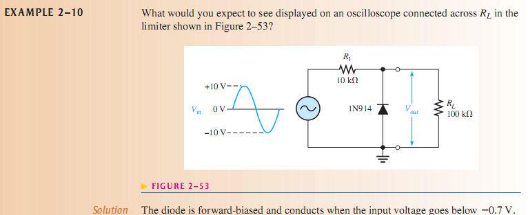
61 63
62 Diode Limiting (Clipping) Circuits What is the output of positive limiter shown? V in 10 V 1.0 kω 0 R 1 R L 3.0 V V BIAS = kω 2.3 V The diode is forward-biased when the output tries to go above =3.0 V. This causes the output to be limited to voltages less than 3.0 V. 64
63 Quiz Q. The bias voltage is set to 4.3 V. The output of the biased limiter shown will be clipped a. above 3.6 V R 1 b. below 3.6 V c. above 5.0 V d. below 5.0 V 10 V 1.0 kω V in 0 V BIAS = 4.3 V R L 100 kω 65
64 Diode Limiting (Clipping) Circuits What happens in the previous circuit if the diode is reversed? 10 V 1.0 kω R 1 V in 0 R L V BIAS = kω 1.6 V 2.3 V The diode is forward-biased when the output tries to go below =1.6 V. This causes the output to be limited to voltages greater than 1.6 V. 66
65 Quiz Q. The bias voltage is set to 4.3 V. The output of the biased limiter shown will be clipped a. above 3.6 V R 1 b. below 3.6 V c. above 5.0 V 10 V 1.0 kω V in 0 V BIAS = 4.3 V R L 100 kω d. below 5.0 V 67

66 68
67 Diode Clamping Circuits A clamper (dc restorer) is a circuit that adds a dc level to an ac signal. A capacitor is in series with the load. A positive clamper is shown. The capacitor is charged to a voltage that is one diode drop less than the peak voltage of the signal. V p(in) 0.7 V V p(in) 0.7 V V p(in) V out 0 R L V 69
68 Positive Clamper Operation Reverse -biased 70
69 Positive Clamper Operation When the input voltage initially goes negative, the diode is forward-biased, allowing the capacitor to charge to near the peak of the input. Just after the negative peak, the diode is reverse-biased. The capacitor can only discharge through the high resistance of R L. So, from the peak of one negative half-cycle to the next, the capacitor discharges very little. The amount that is discharged depends on the value of R L. If the RC time constant is 100 times the period, the clamping action is excellent. An RC time constant of 10 times the period will have a small amount of distortion. The net effect of the clamping action is that the capacitor retains a charge approximately equal to the peak value of the input less the diode drop (0.7 V). The capacitor voltage acts essentially as a battery in series with the input voltage. The dc voltage of the capacitor adds to the input voltage by superposition. 71
70 Diode Clamping Circuits Reversing the diode forms a negative clamper. V p (in) -0.7 V p(in) V 0 R L V out V p (in) 0.7 V 72
71 Quiz Q. The circuit shown is a a. negative clipping circuit b. positive clipping circuit c. negative clamping circuit R L d. positive clamping circuit 73
72 Voltage Multipliers Voltage multipliers use clamping action to increase peak rectified voltages. Half-Wave Voltage Doubler (neglecting the diode drop) 74
 doubled by taking it across both capacitors in series.")
73 Full-Wave Voltage Doubler The full-wave voltage doubler works by charging a capacitor to the positive peak voltage on one cycle of the sine wave and a second capacitor on the negative peak voltage. The output is (ideally) doubled by taking it across both capacitors in series. (neglecting the diode drop) 0 V p D 1 I D 2 Reverse-biased C 1 C 2 V p 0 Reverse-biased V p I D 1 C 1 C 2 D 2 V p V p 2V p 75
74 Quiz Q. The circuit shown is a a. full-wave rectifier D 1 b. full-wave voltage doubler C 1 c. positive clamping circuit d. negative clamping circuit D 2 C 2 76
75 Selected Key Terms Rectifier Filter Regulator Ripple Voltage An electronic circuit that converts ac into pulsating dc; one part of a power supply. In a power supply, the capacitor used to reduce the variation of the output voltage from a rectifier. An electronic device or circuit that maintains an essentially constant output voltage for a range of input voltage or load values; one part of a power supply. The small variation in dc output voltage of a filtered rectifier caused by charging and discharging of the filter capacitor. 77
76 Selected Key Terms Line Regulation Load Regulation Limiter Clamper The change in output voltage of a regulator for a given change in input voltage, normally expressed as a percentage. The change in output voltage of a regulator for a given range of load currents, normally expressed as a percentage. A diode circuit that clips off or removes part of a waveform above and/or below a specified level. A circuit that adds a dc level to an ac voltage using a diode and a capacitor. 78

77 79

78 80
79 81
80 82
Electronic Devices. Floyd. Chapter 2. Ninth Edition. Electronic Devices, 9th edition Thomas L. Floyd
 Electronic Devices Ninth Edition Floyd Chapter 2 Agenda Diode Circuits and Applications Half-wave Rectifier Full-wave Rectifier Power Supply Filter Power Supply Regulator Diode Limiting Circuits Diode
Chapter 2. Diodes & Applications
 Chapter 2 Diodes & Applications The Diode A diode is made from a small piece of semiconductor material, usually silicon, in which half is doped as a p region and half is doped as an n region with a pn
CHAPTER 2. Diode Applications
 CHAPTER 2 Diode Applications 1 Objectives Explain and analyze the operation of both half and full wave rectifiers Explain and analyze filters and regulators and their characteristics Explain and analyze
Lecture (04) PN Diode applications II
 PN Diode applications II") Lecture (04) PN Diode applications II By: Dr. Ahmed ElShafee ١ Agenda Full wave rectifier, cont.,.. Filters Voltage Regulators ٢ RMS The RMS value of a set of values (or a continuous time waveform) is
Lecture (04) PN Diode applications II By: Dr. Ahmed ElShafee ١ Agenda Full wave rectifier, cont.,.. Filters Voltage Regulators ٢ RMS The RMS value of a set of values (or a continuous time waveform) is
Lecture (04) Diode applications, cont.
 Diode applications, cont.") Lecture (04) Diode applications, cont. By: Dr. Ahmed ElShafee Agenda Full wave rectifier, cont.,.. Filters Voltage Regulators Diode limiters Diode Clampers ١ ٢ Bridge Full Wave Rectifier Operation uses
Lecture (04) Diode applications, cont. By: Dr. Ahmed ElShafee Agenda Full wave rectifier, cont.,.. Filters Voltage Regulators Diode limiters Diode Clampers ١ ٢ Bridge Full Wave Rectifier Operation uses
Electronic Circuits. Diode Applications. Dr. Manar Mohaisen Office: F208 Department of EECE
 Electronic Circuits Diode Applications Dr. Manar Mohaisen Office: F208 Email: manar.subhi@kut.ac.kr Department of EECE Review of the Precedent Lecture Doping It is a controlled addition of impurities to
2) The larger the ripple voltage, the better the filter. 2) 3) Clamping circuits use capacitors and diodes to add a dc level to a waveform.
 The larger the ripple voltage, the better the filter. 2) 3) Clamping circuits use capacitors and diodes to add a dc level to a waveform.") TRUE/FALSE. Write 'T' if the statement is true and 'F' if the statement is false. 1) A diode conducts current when forward-biased and blocks current when reverse-biased. 1) 2) The larger the ripple voltage,
TRUE/FALSE. Write 'T' if the statement is true and 'F' if the statement is false. 1) A diode conducts current when forward-biased and blocks current when reverse-biased. 1) 2) The larger the ripple voltage,
Analog Electronics. Lecture 3. Muhammad Amir Yousaf
 Analog Electronics Lecture 3 Discrete Semiconductor Devices Rectifier (Diodes) Light Emitting Diodes Zener Diodes Photo Diodes Transistors Bipolar Junction Transistors (BJTs) MOSFETs Diodes A diode is
CHAPTER 1 DIODE CIRCUITS. Semiconductor act differently to DC and AC currents
 CHAPTER 1 DIODE CIRCUITS Resistance levels Semiconductor act differently to DC and AC currents There are three types of resistances 1. DC or static resistance The application of DC voltage to a circuit
Applications of Diode
 Applications of Diode Diode Approximation: (Large signal operations): 1. Ideal Diode: When diode is forward biased, resistance offered is zero, When it is reverse biased resistance offered is infinity.
Lecture (03) Diodes and Diode Applications I
 Diodes and Diode Applications I") Lecture (03) Diodes and Diode Applications I By: Dr. Ahmed ElShafee ١ Agenda VOLTAGE CURRENT CHARACTERISTIC OF A DIODE Forward bias Reverse Bias V I Characteristic for Forward Bias V I Characteristic for
Lecture (03) Diodes and Diode Applications I By: Dr. Ahmed ElShafee ١ Agenda VOLTAGE CURRENT CHARACTERISTIC OF A DIODE Forward bias Reverse Bias V I Characteristic for Forward Bias V I Characteristic for
RECTIFIERS POWER SUPPLY AND VOLTAGE REGULATION. Rectifier. Basic DC Power Supply. Filter. Regulator
 RECTIFIERS POWER SUPPLY AND OLTAGE REGULATION Prepared by Engr. JP Timola Reference: Electronic Devices by Thomas L. Floyd Because of their ability to conduct current in one direction and block current
Diode Applications 1
 Diode Applications 1 Explain and analyze the operation of both half and full wave rectifiers Explain and analyze filters and regulators and their characteristics Explain and analyze the operation of diode
EXPERIMENT 7: DIODE CHARACTERISTICS AND CIRCUITS 10/24/10
 DIODE CHARACTERISTICS AND CIRCUITS EXPERIMENT 7: DIODE CHARACTERISTICS AND CIRCUITS 10/24/10 In this experiment we will measure the I vs V characteristics of Si, Ge, and Zener p-n junction diodes, and
Lecture 7: Diode Rectifier Circuits (Half Cycle, Full Cycle, and Bridge).
.") Whites, EE 320 Lecture 7 Page 1 of 9 Lecture 7: Diode Rectifier Circuits (Half Cycle, Full Cycle, and Bridge). We saw in the previous lecture that Zener diodes can be used in circuits that provide (1)
Whites, EE 320 Lecture 7 Page 1 of 9 Lecture 7: Diode Rectifier Circuits (Half Cycle, Full Cycle, and Bridge). We saw in the previous lecture that Zener diodes can be used in circuits that provide (1)
Chapter 1 Introduction to Electronics
 Chapter 1 Introduction to Electronics Section 1-1 Atomic Structure 1. An atom with an atomic number of 6 has 6 electrons and 6 protons.. The third shell of an atom can have n = (3) = 18 electrons. Section
Table of Contents. iii
 Table of Contents Subject Page Experiment 1: Diode Characteristics... 1 Experiment 2: Rectifier Circuits... 7 Experiment 3: Clipping and Clamping Circuits 17 Experiment 4: The Zener Diode 25 Experiment
Examples to Power Supply
 Examples to Power Supply Example-1: A center-tapped full-wave rectifier connected to a transformer whose each secondary coil has a r.m.s. voltage of 1 V. Assume the internal resistances of the diode and
Electronic Circuits I - Tutorial 03 Diode Applications I
 Electronic Circuits I - Tutorial 03 Diode Applications I -1 / 13 - T & F # Question 1 A diode can conduct current in two directions with equal ease. F 2 When reverse-biased, a diode ideally appears as
Diodes and Applications
 Diodes and Applications Diodes and Applications 2 1 Diode Operation 2 2 Voltage-Current (V-I) Characteristics 2 3 Diode Models 2 4 Half-Wave Rectifiers 2 5 Full-Wave Rectifiers 2 6 Power Supply Filters
A device which removes the peak of a waveform is known as a Clipper. Voltage clipping diagram
 DIODE CLIPPER A device which removes the peak of a waveform is known as a Clipper Voltage clipping diagram Clipping circuit Clipping circuit is a wave-shaping circuit, and is used to either remove or clip
Zener Diodes. Specifying and modeling the zener diode. - Diodes operating in the breakdown region can be used in the design of voltage regulators.
 Zener Diodes - Diodes operating in the breakdown region can be used in the design of voltage regulators. Specifying and modeling the zener diode Dynamic resistance, r Z a few ohms to a few tens of ohms
3.4. Operation in the Reverse Breakdown
 3.4. peration in the Reverse Breakdown Under certain circumstances, diodes may be intentionally used in the reverse breakdown region These are referred to as Zener Diode or Breakdown Diode Voltage regulator
Diodes (non-linear devices)
") C H A P T E R 4 Diodes (non-linear devices) Ideal Diode Figure 4.2 The two modes of operation of ideal diodes and the use of an external circuit to limit (a) the forward current and (b) the reverse voltage.
C H A P T E R 4 Diodes (non-linear devices) Ideal Diode Figure 4.2 The two modes of operation of ideal diodes and the use of an external circuit to limit (a) the forward current and (b) the reverse voltage.
3.4. Reverse Breakdown Region Zener Diodes In the breakdown region Very steep i-v curve Almost constant voltage drop Used for voltage regulator
 3.4. Reverse Breakdown Region Zener Diodes In the breakdown region Very steep i-v curve Almost constant voltage drop Used for voltage regulator Voltage regulator Provide a constant dc output voltage If
Sheet 2 Diodes. ECE335: Electronic Engineering Fall Ain Shams University Faculty of Engineering. Problem (1) Draw the
 Draw the") Ain Shams University Faculty of Engineering ECE335: Electronic Engineering Fall 2014 Sheet 2 Diodes Problem (1) Draw the i) Charge density distribution, ii) Electric field distribution iii) Potential distribution,
Ain Shams University Faculty of Engineering ECE335: Electronic Engineering Fall 2014 Sheet 2 Diodes Problem (1) Draw the i) Charge density distribution, ii) Electric field distribution iii) Potential distribution,
After performing this experiment, you should be able to:
 Objectives: After performing this experiment, you should be able to: Demonstrate the strengths and weaknesses of the two basic rectifier circuits. Draw the output waveforms for the two basic rectifier
Diode Limiters or Clipper Circuits
 Diode Limiters or Clipper Circuits Circuits which are used to clip off portions of signal voltages above or below certain levels are called limiters or clippers. Types of Clippers Positive Clipper Negative
Clippers limiter circuits Vi > V Vi < V
 Semiconductor Diode Clipper and Clamper Circuits Clippers Clipper circuits, also called limiter circuits, are used to eliminate portion of a signal that are above or below a specified level clip value.
Federal Urdu University of Arts, Science & Technology Islamabad Pakistan SECOND SEMESTER ELECTRONICS - I
 SECOND SEMESTER ELECTRONICS - I BASIC ELECTRICAL & ELECTRONICS LAB DEPARTMENT OF ELECTRICAL ENGINEERING Prepared By: Checked By: Approved By: Engr. Yousaf Hameed Engr. M.Nasim Khan Dr.Noman Jafri Lecturer
(A) im (B) im (C)0.5 im (D) im.
 im (B) im (C)0.5 im (D) im.") Dr. Mahalingam College of Engineering and Technology, Pollachi. (An Autonomous Institution affiliated to Anna University) Regulation 2014 Fourth Semester Electrical and Electronics Engineering 141EE0404
Dr. Mahalingam College of Engineering and Technology, Pollachi. (An Autonomous Institution affiliated to Anna University) Regulation 2014 Fourth Semester Electrical and Electronics Engineering 141EE0404
IENGINEERS- CONSULTANTS QUESTION BANK SERIES ELECTRONICS ENGINEERING 1 YEAR UPTU
 ELECTRONICS ENGINEERING Unit 1 Objectives Q.1 The breakdown mechanism in a lightly doped p-n junction under reverse biased condition is called. (A) avalanche breakdown. (B) zener breakdown. (C) breakdown
EXPERIMENT 2.2 NON-LINEAR OP-AMP CIRCUITS
 2.16 EXPERIMENT 2.2 NONLINEAR OPAMP CIRCUITS 2.2.1 OBJECTIVE a. To study the operation of 741 opamp as comparator. b. To study the operation of active diode circuits (precisions circuits) using opamps,
1 Diodes. 1.1 Diode Models Ideal Diode. ELEN 236 Diodes
 ELEN 236 Diodes 1 Diodes 1.1 Diode Models 1.1.1 Ideal Diode Current through diode is zero for any voltage less than zero i.e. reverse biased case Current through diode is not limited by diode if voltage
Term Roadmap : Materials Types 1. INSULATORS
 Term Roadmap : Introduction to Signal Processing Differentiating and Integrating Circuits (OpAmps) Clipping and Clamping Circuits(Diodes) Design of analog filters Sinusoidal Oscillators Multivibrators
Lecture (03) Diode applications
 Diode applications") Lecture (03) Diode applications By: Dr. Ahmed ElShafee ١ Agenda The Basic DC Power Supply Half wave rectifier Full wave rectifier Filters Voltage Regulators ٢ The Basic DC Power Supply All active electronic
Lecture (03) Diode applications By: Dr. Ahmed ElShafee ١ Agenda The Basic DC Power Supply Half wave rectifier Full wave rectifier Filters Voltage Regulators ٢ The Basic DC Power Supply All active electronic
55:041 Electronic Circuits
 55:041 Electronic Circuits Chapter 1 & 2 A. Kruger Diode Review, Page-1 Semiconductors licon () atoms have 4 electrons in valence band and form strong covalent bonds with surrounding atoms. Section 1.1.2
EXPERIMENT 5 : DIODES AND RECTIFICATION
 EXPERIMENT 5 : DIODES AND RECTIFICATION Component List Resistors, one of each o 2 1010W o 1 1k o 1 10k 4 1N4004 (Imax = 1A, PIV = 400V) Diodes Center tap transformer (35.6Vpp, 12.6 VRMS) 100 F Electrolytic
Shankersinh Vaghela Bapu Institute of Technology INDEX
 Shankersinh Vaghela Bapu Institute of Technology Diploma EE Semester III 3330905: ELECTRONIC COMPONENTS AND CIRCUITS INDEX Sr. No. Title Page Date Sign Grade 1 Obtain I-V characteristic of Diode. 2 To
Shankersinh Vaghela Bapu Institute of Technology
 Shankersinh Vaghela Bapu Institute of Technology B.E. Semester III (EC) 131101: Basic Electronics INDEX Sr. No. Title Page Date Sign Grade 1 [A] To Study the V-I characteristic of PN junction diode. [B]
UNIVERSITY OF NORTH CAROLINA AT CHARLOTTE. Department of Electrical and Computer Engineering
 UNIVERSITY OF NORTH CAROLINA AT CHARLOTTE Department of Electrical and Computer Engineering Experiment No. 2 - Semiconductor Diodes Overview: In this lab session students will investigate I-V characteristics
EXPERIMENT 5 : THE DIODE
 EXPERIMENT 5 : THE DIODE Component List Resistors, one of each o 1 10 10W o 1 1k o 1 10k 4 1N4004 (Imax = 1A, PIV = 400V) Diodes Center tap transformer (35.6Vpp, 12.6 VRMS) 100 F Electrolytic Capacitor
RECTIFIERS AND POWER SUPPLIES
 UNIT V RECTIFIERS AND POWER SUPPLIES Half-wave, full-wave and bridge rectifiers with resistive load. Analysis for Vdc and ripple voltage with C,CL, L-C and C-L-C filters. Voltage multipliers Zenerdiode
Electronic I Lecture 3 Diode Rectifiers. By Asst. Prof Dr. Jassim K. Hmood
 Electronic I Lecture 3 Diode Rectifiers By Asst. Prof Dr. Jassim K. Hmood Diode Approximations 1- The Ideal Model When forward biased, act as a closed (on) switch When reverse biased, act as open (off)
EXPERIMENT 5 : THE DIODE
 EXPERIMENT 5 : THE DIODE Component List Resistors, one of each o 1 10 10W o 1 1k o 1 10k 4 1N4004 (I max = 1A, PIV = 400V) Diodes Center tap transformer (35.6V pp, 12.6 V RMS ) 100 F Electrolytic Capacitor
VTU NOTES QUESTION PAPERS NEWS RESULTS FORUMS TESTING OF HALF WAVE, FULL WAVE AND BRIDGE RECTIFIERS WITH AND WITHOUT CAPACITOR
 TESTING OF HALF WAVE, FULL WAVE AND BRIDGE RECTIFIERS WITH AND WITHOUT CAPACITOR Aim: To determine the ripple factor, efficiency and regulation of the half wave, full wave and bridge rectifier circuits
EE351 Laboratory Exercise 1 Diode Circuits
 revised July 19, 2009 The purpose of this laboratory exercise is to gain experience and understanding working with diodes. Focus on taking good data so that the plots and calculations you will do later
Chapter #4: Diodes. from Microelectronic Circuits Text by Sedra and Smith Oxford Publishing
 Chapter #4: Diodes from Microelectronic Circuits Text by Sedra and Smith Oxford Publishing Introduction IN THIS CHAPTER WE WILL LEARN the characteristics of the ideal diode and how to analyze and design
Dev Bhoomi Institute Of Technology Department of Electronics and Communication Engineering PRACTICAL INSTRUCTION SHEET
 Dev Bhoomi Institute Of Technology Department of Electronics and Communication Engineering PRACTICAL INSTRUCTION SHEET LABORATORY MANUAL EXPERIMENT NO. ISSUE NO. : ISSUE DATE: REV. NO. : REV. DATE : PAGE:
Circuit operation Let s look at the operation of this single diode rectifier when connected across an alternating voltage source v s.
 Diode Rectifier Circuits One of the important applications of a semiconductor diode is in rectification of AC signals to DC. Diodes are very commonly used for obtaining DC voltage supplies from the readily
ชาว ศวกรรมคอมพ วเตอร คณะว ศวกรรมศาสตร มหาว ทยาล ยเทคโนโลย ราชมงคลพระนคร
 EN2042102 วงจรไฟฟ าและอ เล กทรอน กส Circuits and Electronics บทท 6 ไดโอด Diode สาขาว ชาว ศวกรรมคอมพ วเตอร คณะว ศวกรรมศาสตร มหาว ทยาล ยเทคโนโลย ราชมงคลพระนคร Objectives Explain and analyze the operation
Electronics 1 Lab (CME 2410) Part I - Diode Clipper
 Part I - Diode Clipper") Electronics 1 Lab (CME 2410) School of Informatics & Computing German Jordanian University Laboratory Experiment (3) Prelab: 1. Simulate the procedure describe in Part I, Section 5d (Negative Polarized
Electronics 1 Lab (CME 2410) School of Informatics & Computing German Jordanian University Laboratory Experiment (3) Prelab: 1. Simulate the procedure describe in Part I, Section 5d (Negative Polarized
CHAPTER 5: REGULATED DC POWER SUPPLY
 CHAPTER 5: REGULATED DC POWER SUPPLY Dr. Wan Mahani Hafizah binti Wan Mahmud Topics in Chapter 5 5.0Introduction 5.1Rectifier 5.2Filter 5.3oltage Regulator 5.4Switching Regulator 2 Power Supply Block Diagram
Page 1. Date 15/02/2013
 Page 1 Date 15/02/2013 Final Term Examination Fall 2012 Phy301-Circuit Theory 1. State kirchhoff s current law (KCL) Marks: 2: Answer: (PAGE 42) KIRCHHOF S CURRENT LAW Sum of all the currents entering
55:041 Electronic Circuits
 55:041 Electronic Circuits Chapter 1 & 2 A. Kruger Diode Review, Page-1 Semiconductors licon () atoms have 4 electrons in valence band and form strong covalent bonds with surrounding atoms. Section 1.1.2
Analog Electronic Circuits
 Analog Electronic Circuits Chapter 1: Semiconductor Diodes Objectives: To become familiar with the working principles of semiconductor diode To become familiar with the design and analysis of diode circuits
Diode Applications Half-Wave Rectifying
 Lab 5 Diode Applications Half-Wave ectifying Objectives: Study the half-wave rectifying and smoothing with a capacitor for a simple diode circuit. Study the use of a Zener diode in a circuit with an AC
Lec (03) Diodes and Applications
 Diodes and Applications") Lec (03) Diodes and Applications Diode Models 1 Diodes and Applications Diode Operation V-I Characteristics of a Diode Diode Models Half-Wave and Full-Wave Rectifiers Power Supply Filters and Regulators
Lec (03) Diodes and Applications Diode Models 1 Diodes and Applications Diode Operation V-I Characteristics of a Diode Diode Models Half-Wave and Full-Wave Rectifiers Power Supply Filters and Regulators
3. Diode, Rectifiers, and Power Supplies
 3. Diode, Rectifiers, and Power Supplies Semiconductor diodes are active devices which are extremely important for various electrical and electronic circuits. Diodes are active non-linear circuit elements
CHAPTER 4 FULL WAVE RECTIFIER. AC DC Conversion
 CHAPTER 4 FULL WAVE RECTIFIER AC DC Conversion SINGLE PHASE FULL-WAVE RECTIFIER The objective of a full wave rectifier is to produce a voltage or current which is purely dc or has some specified dc component.
Diodes & Rectifiers Nafees Ahamad
 Diodes & Rectifiers Nafees Ahamad Asstt. Prof., EECE Deptt, DIT University, Dehradun Website: www.eedofdit.weebly.com 1 Diodes Electronic devices created by bringing together a p-type and n-type region
EXPERIMENT 5 : THE DIODE
 EXPERIMENT 5 : THE DIODE Equipment List Dual Channel Oscilloscope R, 330, 1k, 10k resistors P, Tri-Power Supply V, 2x Multimeters D, 4x 1N4004: I max = 1A, PIV = 400V Silicon Diode P 2 35.6V pp (12.6 V
Exercise 3: EXERCISE OBJECTIVE
 Exercise 3: EXERCISE OBJECTIVE voltage equal to double the peak ac input voltage by using a voltage doubler circuit. You will verify your results with a multimeter and an oscilloscope. DISCUSSION times
Experiments in Analog Electronics
 Ministry of Higher Education and Scientific Research University of Technology Department of Electrical Engineering Analog Electronics Laboratory Experiments in Analog Electronics By Firas Mohammed Ali
Electronic Circuits I Laboratory 03 Rectifiers
 Electronic Circuits I Laboratory 03 Rectifiers # Student ID Student Name Grade (10) 1 Instructor signature 2 3 4 5 Delivery Date -1 / 18 - Objectives In this experiment, you will get to know a group of
Diode Bridges. Book page
 Diode Bridges Book page 450-454 Rectification The process of converting an ac supply into dc is called rectification The device that carries this out is called a rectifier Half wave rectifier only half
An Introduction to Rectifier Circuits
 TRADEMARK OF INNOVATION An Introduction to Rectifier Circuits An important application of the diode is one that takes place in the design of the rectifier circuit. Simply put, this circuit converts alternating
ENG2210 Electronic Circuits. Chapter 3 Diodes
 ENG2210 Electronic Circuits Mokhtar A. Aboelaze York University Chapter 3 Diodes Objectives Learn the characteristics of ideal diode and how to analyze and design circuits containing multiple diodes Learn
EE 105. Diode Circuits. Prof. Ali M. Niknejad and Prof. Rikky Muller. U.C. Berkeley Copyright c 2017 by Ali M. Niknejad
 EE 105 Diode Circuits Prof. Ali M. Niknejad and Prof. Rikky Muller U.C. Berkeley Copyright c 2017 by Ali M. Niknejad March 2, 2017 1 / 23 Diode Introduction A diode is a non-linear element. To a very good
Scheme - G. Sample Test Paper-I
 Scheme - G Sample Test Paper-I Course Name : Electronics Engineering Group Course Code : DE/ED/EI/EJ/EN/ET/EV/EX/IC/IE/IS/IU/MU Semester : Second Subject Title : Elements of Electronics 17215 Marks : 25
About the Tutorial. Audience. Prerequisites. Copyright & Disclaimer. Linear Integrated Circuits Applications
 About the Tutorial Linear Integrated Circuits are solid state analog devices that can operate over a continuous range of input signals. Theoretically, they are characterized by an infinite number of operating
Scheme I Sample. : Second : Basic. Electronics : 70. Marks. Time: 3 Hrs. 2] b) State any. e) State any. Figure Definition.
![Scheme I Sample. : Second : Basic. Electronics : 70. Marks. Time: 3 Hrs. 2] b) State any. e) State any. Figure Definition.](/thumbs/96/128002629.jpg "Scheme I Sample. : Second : Basic. Electronics : 70. Marks. Time: 3 Hrs. 2] b) State any. e) State any. Figure Definition.") Program Name Program Code Semester Course Title Scheme I Sample Question Paper : Diploma in Electronics Program Group : DE/EJ/IE/IS/ET/EN/EX : Second : Basic Electronics : 70 22216 Time: 3 Hrs. Instructions:
Program Name Program Code Semester Course Title Scheme I Sample Question Paper : Diploma in Electronics Program Group : DE/EJ/IE/IS/ET/EN/EX : Second : Basic Electronics : 70 22216 Time: 3 Hrs. Instructions:
Objective Type Questions 1. Why pure semiconductors are insulators at 0 o K? 2. What is effect of temperature on barrier voltage? 3.
 Objective Type Questions 1. Why pure semiconductors are insulators at 0 o K? 2. What is effect of temperature on barrier voltage? 3. What is difference between electron and hole? 4. Why electrons have
EXPERIMENT 4 LIMITER AND CLAMPER CIRCUITS
 EXPERIMENT 4 LIMITER AND CLAMPER CIRCUITS 1. OBJECTIVES 1.1 To demonstrate the operation of a diode limiter. 1.2 To demonstrate the operation of a diode clamper. 2. INTRODUCTION PART A: Limiter Circuit
Fundamentals of Microelectronics
 Fundamentals of Microelectronics CH1 Why Microelectronics? CH2 Basic Physics of Semiconductors CH3 Diode Circuits CH4 Physics of Bipolar Transistors CH5 Bipolar Amplifiers CH6 Physics of MOS Transistors
 FINALTERM EXAMINATION Fall 2009 PHY301- Circuit Theory (Session - 2) Time: 120 min Marks: 70 Question No: 1 ( Marks: 1 ) - Please choose one Charge of 2c and 5c will attract each other repel each other
Practical Manual. Deptt.of Electronics &Communication Engg. (ECE)
") Practical Manual LAB: BASICS OF ELECTRONICS 1 ST SEM.(CSE/CV) Deptt.of Electronics &Communication Engg. (ECE) RAO PAHALD SINGH GROUP OF INSTITUTIONS BALANA(MOHINDER GARH)12302 Prepared By. Mr.SANDEEP KUMAR
Practical Manual LAB: BASICS OF ELECTRONICS 1 ST SEM.(CSE/CV) Deptt.of Electronics &Communication Engg. (ECE) RAO PAHALD SINGH GROUP OF INSTITUTIONS BALANA(MOHINDER GARH)12302 Prepared By. Mr.SANDEEP KUMAR
Experiment #2 Half Wave Rectifier
 PURPOSE: ELECTRONICS 224 ETR620S Experiment #2 Half Wave Rectifier This laboratory session acquaints you with the operation of a diode power supply. You will study the operation of half-wave and the effect
WINTER 14 EXAMINATION. Model Answer. Subject Code: ) The answers should be examined by key words and not as word-to-word as given in the
 The answers should be examined by key words and not as word-to-word as given in the") Subject Code: 17215 WINTER 14 EXAMINATION Model Answer Important Instructions to examiners: 1) The answers should be examined by key words and not as word-to-word as given in the model answer scheme. 2)
Subject Code: 17215 WINTER 14 EXAMINATION Model Answer Important Instructions to examiners: 1) The answers should be examined by key words and not as word-to-word as given in the model answer scheme. 2)
Ching-Yuan Yang. (symbol) Called breakdown diode or Zener diode, it can be used as voltage regulator. Breakdown voltage V ZK
 Called breakdown diode or Zener diode, it can be used as voltage regulator. Breakdown voltage V ZK") Diodes Read Chapter 3, Section 3.4-3.6, 3.9 Sedra/Smith s Microelectronic Circuits Ching-Yuan Yang National Chung Hsing University Department of Electrical Engineering Zener diode Operate in the reverse
Diodes Read Chapter 3, Section 3.4-3.6, 3.9 Sedra/Smith s Microelectronic Circuits Ching-Yuan Yang National Chung Hsing University Department of Electrical Engineering Zener diode Operate in the reverse
NORTHWESTERN UNIVERSITY TECHNOLOGICAL INSTITUTE
 NORTHWESTERN UNIVERSITY TECHNOLOGICAL INSTITUTE ECE-270 Experiment #4 X-Y DISPLAY TECHNIQUES: DIODE CHARACTERISTICS PRELAB Use your textbook and/or the library to answer the following questions about diodes.
2 MARKS EE2203 ELECTRONIC DEVICES AND CIRCUITS UNIT 1
 2 MARKS EE2203 ELECTRONIC DEVICES AND CIRCUITS UNIT 1 1. Define PN junction. When a p type semiconductor is joined to a N type semiconductor the contact surface is called PN junction. 2. What is an ideal
EXPERIMENT 3 Half-Wave and Full-Wave Rectification
 Name & Surname: ID: Date: EXPERIMENT 3 Half-Wave and Full-Wave Rectification Objective To calculate, compare, draw, and measure the DC output voltages of half-wave and full-wave rectifier circuits. Tools
Lecture -1: p-n Junction Diode
 Lecture -1: p-n Junction Diode Diode: A pure silicon crystal or germanium crystal is known as an intrinsic semiconductor. There are not enough free electrons and holes in an intrinsic semi-conductor to
Document Name: Electronic Circuits Lab. Facebook: Twitter:
 Document Name: Electronic Circuits Lab www.vidyathiplus.in Facebook: www.facebook.com/vidyarthiplus Twitter: www.twitter.com/vidyarthiplus Copyright 2011-2015 Vidyarthiplus.in (VP Group) Page 1 CIRCUIT
EET1240/ET212 EET1240/ET212
 EET1240/ET212 Electronics Semiconductors and Diodes Electrical and Telecommunications Engineering Technology Department Prepared by textbook based on Electronics Devices by Floyd, Prentice Hall, 7 th edition.
Part I Lectures 1-7 Diode Circuit Applications
 Part Lectures -7 iode Circuit Applications The PN Junction iode Electrical and Electronic Engineering epartment Lecture One - Page of 7 Second Year, Electronics, 9 - The PN Junction iode Basic Construction:
Diode Characteristics and Applications
 Diode Characteristics and Applications Topics covered in this presentation: Diode Characteristics Diode Clamp Protecting Against Back-EMF Half-Wave Rectifier The Zener Diode 1 of 18 Diode Characteristics
ECE321 Electronics I
 ECE321 Electronics Lecture 2: Basic Circuits with Diodes Payman Zarkesh-Ha Office: ECE Bldg. 230B Office hours: Tuesday 2:00-3:00PM or by appointment E-mail: pzarkesh.unm.edu Slide: 1 Review of Last Lecture
SILVER OAK COLLEGE OF ENGINEERING & TECHNOLOGY ADITYA SILVER OAK INSTITUTE OF TECHNOLOGY
 Enroll. No. SILVER OAK COLLEGE OF ENGINEERING & TECHNOLOGY ADITYA SILVER OAK INSTITUTE OF TECHNOLOGY BE - SEMESTER 3 MID SEMESTER-I EXAMINATION WINTER 2017 SUBJECT: Advanced Engineering Mathematics (2130002)
State the application of negative feedback and positive feedback (one in each case)
") (ISO/IEC - 700-005 Certified) Subject Code: 073 Model wer Page No: / N Important Instructions to examiners: ) The answers should be examined by key words and not as word-to-word as given in the model answer
(ISO/IEC - 700-005 Certified) Subject Code: 073 Model wer Page No: / N Important Instructions to examiners: ) The answers should be examined by key words and not as word-to-word as given in the model answer
Precision Rectifier Circuits
 Precision Rectifier Circuits Rectifier circuits are used in the design of power supply circuits. In such applications, the voltage being rectified are usually much greater than the diode voltage drop,
Homework Assignment 04
 Question 1 (Short Takes) Homework Assignment 04 1. Consider the single-supply op-amp amplifier shown. What is the purpose of R 3? (1 point) Answer: This compensates for the op-amp s input bias current.
ES736 True RMS-to-DC Converters
 Features True RMS-to-DC Conversion Fast settling time for all input levels Input level is specified up to 400mV RMS (Crest factor < 3 at 3V power) Averaging capacitor is typically 22uF Positive output
FET Channel. - simplified representation of three terminal device called a field effect transistor (FET)
") FET Channel - simplified representation of three terminal device called a field effect transistor (FET) - overall horizontal shape - current levels off as voltage increases - two regions of operation 1.
FET Channel - simplified representation of three terminal device called a field effect transistor (FET) - overall horizontal shape - current levels off as voltage increases - two regions of operation 1.
INC 253 Digital and electronics laboratory I
 INC 253 Digital and electronics laboratory I Laboratory 4 Wave Shaping Diode Circuits Author: ID CoAuthors: 1. ID 2. ID 3. ID Experiment Date: Report received Date: Comments For Instructor Full Marks Pre
Lecture 3 Diodes & Applications :Outline
 Lecture 3 Diodes & Applications :Outline Introduction Diode biasing Diode model Testing a diode Diode application: Rectifiers Diode application: Voltage multipliers Diode application: Optoelectronics 1
Summer 2015 Examination. 1) The answers should be examined by key words and not as word-to-word as given in the model answer scheme.
 The answers should be examined by key words and not as word-to-word as given in the model answer scheme.") Summer 2015 Examination Subject Code: 17215 Model Answer Important Instructions to examiners: 1) The answers should be examined by key words and not as word-to-word as given in the model answer scheme.
Summer 2015 Examination Subject Code: 17215 Model Answer Important Instructions to examiners: 1) The answers should be examined by key words and not as word-to-word as given in the model answer scheme.
OBJECTIVE TYPE QUESTIONS FOR PRACTICAL EXAMINATION Subject : Electronics-I ( EC 112)
") OBJECTIVE TYPE QUESTIONS FOR PRACTICAL EXAMINATION Subject : Electronics-I ( EC 112) 1. Which mathematical notation specifies the condition of periodicity for a continuous time signal? a. x(t) = x( t +T)
OBJECTIVE TYPE QUESTIONS FOR PRACTICAL EXAMINATION Subject : Electronics-I ( EC 112) 1. Which mathematical notation specifies the condition of periodicity for a continuous time signal? a. x(t) = x( t +T)
1. An engineer measures the (step response) rise time of an amplifier as. Estimate the 3-dB bandwidth of the amplifier. (2 points)
 rise time of an amplifier as. Estimate the 3-dB bandwidth of the amplifier. (2 points)") Exam 1 Name: Score /60 Question 1 Short Takes 1 point each unless noted otherwise. 1. An engineer measures the (step response) rise time of an amplifier as. Estimate the 3-dB bandwidth of the amplifier.
Exam 1 Name: Score /60 Question 1 Short Takes 1 point each unless noted otherwise. 1. An engineer measures the (step response) rise time of an amplifier as. Estimate the 3-dB bandwidth of the amplifier.