Module 2: CMOS FEOL Analysis
|
|
|
- Beverly Wilson
- 5 years ago
- Views:
Transcription
1 Module 2: CMOS FEOL Analysis
2 Manufacturer Device # 2 About Chipworks Chipworks is the recognized leader in reverse engineering and patent infringement analysis of semiconductors and electronic systems. The company s ability to analyze the circuitry and physical composition of these systems makes them a key partner in the success of the world s largest semiconductor and microelectronics companies. Intellectual property groups and their legal counsel trust Chipworks for success in patent licensing and litigation earning hundreds of millions of dollars in patent licenses, and saving as much in royalty payments. Research & Development and Product Management rely on Chipworks for success in new product design and launch, saving hundreds of millions of dollars in design, and earning even more through superior product design and faster launches. Contact Chipworks To find out more information on this report, or any other reports in our library, please contact Chipworks at Chipworks 3685 Richmond Road, Suite 500 Ottawa, Ontario K2H 5B7 Canada T F Web site: com info@chipworks.com
3 Manufacturer Device # 3 Some of the information is this report may be covered by patents, mask and/or copyright protection. This report should not be taken as an inducement to infringe on these rights Chipworks Inc. This report is provided exclusively for the use of the purchasing organization. It can be freely copied and distributed within the purchasing organization, conditional upon the accompanying Chipworks accreditation remaining attached. Distribution of the entire report outside of the purchasing organization is strictly forbidden. The use of portions of the document for the support of the purchasing organization s corporate interest (e.g., licensing or marketing activities) is permitted, as defined by the fair use provisions of the copyright act. Accreditation to Chipworks must be attached to any yportion of the reproduced information. Report Code: IPR-XXXX-XXX.1 LOA# Revision XX Published: XX
4 Manufacturer Device # 4 Table of Contents (all CMOS Modules) Module 1: CMOS Overview Analysis Package photographs Package X-rays Determination of technology node based on SEM cross section Module 2: CMOS FEOL Analysis SEM and TEM analysis of isolation, MOS transistors and PMD Selected Materials analysis results SCM and SRP or SIMS analysis of wells Critical dimensions Module 3:CMOS BEOL Analysis SEM and TEM cross-sectional analysis of dielectrics, metals and vias. Materials analysis results for metals and dielectrics Critical dimensions Module 4:CMOS SRAM Analysis Plan-view analysis of minimum SRAM cell Cross-sectional SEM and TEM analysis of SRAM cell
5 Manufacturer Device # 5 Summary Slide Introduction Device Identification Process Summary Observed Critical Dimensions FEOL Analysis PMD TEM Contact Bottom and Silicide TEM NMOS and PMOS SEM Silicon Etch MOS Transistor TEM Contacted MOS Gates MOS Gate Detail MOS Gate Wrap MOS Gate Wrap Detail Gate Dielectric STI Depth Minimum Width STI Substrate Doping Analysis SCM of Wells SIMS of Logic Area (optional) Statement of Measurement Uncertainty and Scope Variation
6 Manufacturer Device # 6 Introduction The 45 nm XXXXXXXX was extracted from a XXXXXXX. [1] reference
7 Manufacturer Device # 7 Device Identification Manufacturer XXXXXXXXXX Foundry XXXXXXXXXX Part number XXXXXXXXXX Type XXXXXXXXXX Date code XXXXXXXXXX Package markings Package type XXXXXXXXXX XXXXXXXXXX XXXXXXXXXX BGA Package dimensions XX.X mm x XX.X mm x X.X mm thick Die markings XXXXXXXXXX Die size (die edge seal) 8.42 mm x 8.14 mm (65.5 mm2)
8 Manufacturer Device # 8 Process Summary Process type CMOS Number of metal layers 9 Minimum MOS transistor gate length 32 nm Process generation 45 nm Feature measured to determine process generation Contacted gate pitch and MOS gate length
9 Manufacturer Device # 9 Observed Critical Dimensions Width (µm) Space (µm) Pitch (µm) Thickness (µm) Metal Contacted Gates 0.18 Minimum MOS Gate Length 32 nm 0.11 Minimum STI
10 Manufacturer Device # 10 FEOL Analysis TEM and SEM cross-sectional analysis of metal 1, PMD, transistors and STI is included.


11 Manufacturer Device # 11 PMD TEM PMD 5 SiOC PMD 4 oxide M1 Cu PMD 3 oxide PMD 2 oxide 0.44 µm W contact PMD 1 - SiON poly gate NiSi NiSi


12 Manufacturer Device # 12 Contact Bottom and Silicide TEM W contact TiN liner ~5 nm ~12 nm NiSi ~8 nm Si substrate Contact bottom
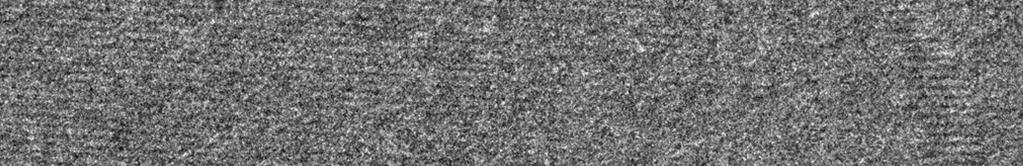
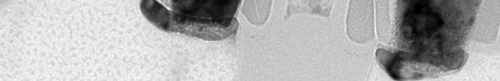
13 Manufacturer Device # 13 NMOS and PMOS SEM Silicon Etch NMOS PMOS


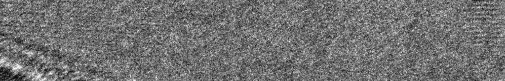
14 Manufacturer Device # 14 MOS Transistor TEM NiSi buffer oxide silicon nitride SWS polysilicon 32 nm NMOS and PMOS have the same physical structure


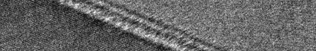
15 Manufacturer Device # 15 Contacted MOS Gates NiSi 30 nm 50 nm 190 nm 24 nm 40 nm 32 nm notch NiSi 29 nm 36 nm 33 nm
16 Manufacturer Device # 16 MOS Gate Detail NiSi buffer oxide 13 nm SiON CESL W contact 27 nm polysilicon ONO gate dielectric silicon nitride SWS 7 nm 22 nm 38 nm NiSi Si substrate


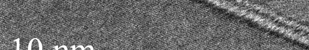
17 Manufacturer Device # 17 MOS Gate Wrap 16 nm NiSi 108 nm polysilicon 11 nm Si substrate STI


18 Manufacturer Device # 18 MOS Gate Wrap Detail polysilicon gate dielectric 13 nm Si substrate STI
19 Manufacturer Device # 19 Gate Dielectric polysilicon O N O 2.0 nm Si 2.0 nm ONO gate dielectric
20 Manufacturer Device # 20 STI Depth


21 Manufacturer Device # 21 Minimum Width STI W contact poly 0.11 µm 0.32 µm
22 Manufacturer Device # 22 Substrate Doping Analysis A combination of SCM plus either SRP or SIMS analysis of the substrate doping is included.


.")
23 Manufacturer Device # 23 SCM of Wells metals and dielectrics P-type N-well P-well highly-doped/ undoped P-epi N-type P-substrate SCM is a scanning probe microscopy method that is sensitive to the semiconductor dopant type. N-type materials give a negative response (yellow) while P-type materials give a positive response (blue-purple). Highly doped and undoped semiconductor materials give a null response.
24 Manufacturer Device # 24 SIMS of Logic Area (optional) Boron Doped P-Wells As and P Doped N-Wells 1E+21 1.E+05 1E+21 B11 1E+20 STI O P31 As75 O18 1.E+04 Atom Con nc (cm -3 ) 1E+20 1E+19 1E E+17 1E+19 B 1E+18 Conc (cm -3 ) Atom 1E+17 As P 1.E+03 1.E+02 ensity (c/s) Inte 1E+16 1E+16 1.E+01 1E Depth (µm) 1E+15 1.E Depth (µm) SIMS profiling of the dopants is provided with the CMOS FEOL Module. This SIMS analysis is performed in an area of dense logic, and hence the profile includes both N and P-well areas. The data has not bee corrected for the relative analysis areas. SRP may be substituted for SIMS in the CMOS FEOL Module
25 Manufacturer Device # 25 Statement of Measurement Uncertainty and Scope Variation Measurement Uncertainty Chipworks calibrates length measurements on its scanning electron microscopes (SEM), transmission electron microscope (TEM), and optical microscopes, using measurement standards that are traceable to the International System of Units (SI). Our SEM/TEM cross-calibration calibration standard was calibrated at the National Physical Laboratory (NPL) in the UK (Report Reference LR0304/E /SEM4/190). This standard has a 146 ± 2 nm (± 1.4%) pitch, as certified by NPL. Chipworks regularly verifies that its SEM and TEM are calibrated to within ± 2% of this standard, over the full magnification ranges used. Fluctuations in the tool performance, coupled with variability in sample preparation, and random errors introduced during analyses of the micrographs, yield an expanded uncertainty of about ± 5%. A stage micrometer, calibrated at the National Research Council of Canada (CNRC) (Report Reference LS ), 0010) is used to calibrate Chipworks optical microscopes. This standard has an expanded uncertainty of 0.3 µm for the stage micrometer s 100 µm pitch lines. Random errors, during analyses of optical micrographs, yield an expanded uncertainty of approximately ± 5% to the measurements. The materials analysis reported in Chipworks reports is normally limited to approximate elemental composition, rather than stoichiometry, since calibration of our SEM and TEM based methods is not feasible. Chipworks will typically abbreviate, using only the elemental symbols, rather than full chemical formulae, usually starting with silicon or the metallic element, then in approximate order of decreasing atomic % (when known). Elemental labels on energy dispersive X-ray spectra (EDS) will be colored red for spurious peaks (elements not originally in sample). Elemental labels in blue correspond to interference from adjacent layers. Secondary ion mass spectrometry (SIMS) data may be calibrated for certain dopant elements, provided suitable standards were available. Scope Variation Due to the nature of reverse engineering, there is a possibility of minor content variation in Chipworks standard reports. Chipworks has a defined table of contents for each standard report type. At a minimum, the defined content will be included in the report. However, depending on the nature of the analysis, additional information may be provided in a report as value-added material for our customers.
26 Manufacturer Device # 26 About Chipworks Chipworks is the recognized leader in reverse engineering and patent infringement analysis of semiconductors and electronic systems. The company s ability to analyze the circuitry and physical composition of these systems makes them a key partner in the success of the world s largest semiconductor and microelectronics companies. Intellectual property groups and their legal counsel trust Chipworks for success in patent licensing and litigation earning hundreds of millions of dollars in patent licenses, and saving as much in royalty payments. Research & Development and Product Management rely on Chipworks for success in new product design and launch, saving hundreds of millions of dollars in design, and earning even more through superior product design and faster launches. Contact Chipworks To find out more information on this report, or any other reports in our library, please contact Chipworks at Chipworks 3685 Richmond Road, Suite 500 Ottawa, Ontario K2H 5B7 Canada T F Web site: com info@chipworks.com
Manufacturer Part Number. Module 4: CMOS SRAM Analysis
 Manufacturer Part Number description Module 4: CMOS SRAM Analysis Manufacturer Device # 2 Some of the information is this report may be covered by patents, mask and/or copyright protection. This report
AKM AK8973 and AK Axis Electronic Compass
 AKM AK8973 and AK8974 Process Review For comments, questions, or more information about this report, or for any additional technical needs concerning semiconductor and electronics technology, please call
Basic Functional Analysis. Sample Report Richmond Road, Suite 500, Ottawa, ON K2H 5B7 Canada Tel:
 Basic Functional Analysis Sample Report 3685 Richmond Road, Suite 500, Ottawa, ON K2H 5B7 Canada Tel: 613-829-0414 www.chipworks.com Basic Functional Analysis Sample Report Some of the information in this
Layout Analysis Floorplan
 Sample Report Analysis from a Touch Screen Controller For any additional technical needs concerning semiconductor and electronics technology, please call Sales at Chipworks. 3685 Richmond Road, Suite 500,
Qualcomm MDM9215M Gobi 4G GSM/CDMA Modem 28 nm LP. Module 2: CMOS FEOL Analysis
 Qualcomm MDM9215M Gobi 4G GSM/CDMA Modem 28 nm LP Module 2: CMOS FEOL Analysis Qualcomm MDM9215M Gobi 4G GSM/CDMA Modem 28 nm LP 2 Some of the information in this report may be covered by patents, mask
Rockchip RK3188 Mobile Application Processor GF 28 nm SLP Gate First HKMG CMOS Process
 Rockchip RK3188 Mobile Application Processor GF 28 nm SLP Gate First HKMG CMOS Process Process Review FEOL Analysis 1891 Robertson Road, Suite 500, Ottawa, ON K2H 5B7 Canada Tel: 613-829-0414 www.chipworks.com
Texas Instruments Sitara XAM3715CBC Application Processor 45 nm UMC Low Power Process
 Texas Instruments Sitara XAM3715CBC Application Processor Structural Analysis For comments, questions, or more information about this report, or for any additional technical needs concerning semiconductor
STMicroelectronics VL53L0B ToF Proximity Sensor
 STMicroelectronics VL53L0B Basic Functional Analysis 1891 Robertson Road, Suite 500, Ottawa, ON K2H 5B7 Canada Tel: 613-829-0414 chipworks.com Basic Functional Analysis 2 Some of the information in this
Nikon NC81369R 24.2 Mp, 3.8 µm Pixel Size, APS-C Format CMOS Image Sensor from the Nikon D3200. Module 5: Substrate Dopant Analysis
 Nikon NC81369R 24.2 Mp, 3.8 µm Pixel Size, APS-C Format CMOS Image Sensor from the Nikon D3200 Module 5: Substrate Dopant Analysis Nikon NC81369R CMOS Image Sensor from the Nikon D3200 2 Some of the information
Bosch Sensortec BMI160 Low Power IMU
 Bosch Sensortec BMI160 Basic Functional Analysis 1891 Robertson Road, Suite 500, Ottawa, ON K2H 5B7 Canada Tel: 613-829-0414 chipworks.com Basic Functional Analysis 2 Some of the information in this report
Goodix GF6648 Touch Fingerprint Sensor. Exploratory Analysis
 Goodix GF6648 Exploratory Analysis 2 Some of the information in this report may be covered by patents, mask and/or copyright protection. This report should not be taken as an inducement to infringe on
Sony IMX Mp, 4.8 µm Pixel Size APS-C (DX Format) CMOS Image Sensor from Nikon D7000. Module 5: Substrate Dopant Analysis
 CMOS Image Sensor from Nikon D7000. Module 5: Substrate Dopant Analysis") Sony IMX071 16.2 Mp, 4.8 µm Pixel Size APS-C (DX Format) CMOS Image Sensor from Nikon D7000 Module 5: Substrate Dopant Analysis Sony IMX071 16.2 Mp, 4.8 µm Pixel Size, APS-C (DX Format) CMOS Image Sensor
Sony IMX071 16.2 Mp, 4.8 µm Pixel Size APS-C (DX Format) CMOS Image Sensor from Nikon D7000 Module 5: Substrate Dopant Analysis Sony IMX071 16.2 Mp, 4.8 µm Pixel Size, APS-C (DX Format) CMOS Image Sensor
Nikon NC81369R 24.2 Mp, 3.8 µm Pixel Size, APS-C Format CMOS Image Sensor from the Nikon D3200. Module 4: Pixel Cross-Sectional Analysis
 Nikon NC81369R 24.2 Mp, 3.8 µm Pixel Size, APS-C Format CMOS Image Sensor from the Nikon D3200 Module 4: Pixel Cross-Sectional Analysis Nikon NC81369R (CMOS Image Sensor from the Nikon D3200) 2 Some of
Altera 5SGXEA7K2F40C2ES Stratix V TSMC 28 nm HP Gate Last HKMG CMOS Process
 Altera 5SGXEA7K2F40C2ES Stratix V TSMC 28 nm HP Gate Last HKMG CMOS Process Process Review FEOL Analysis 3685 Richmond Road, Suite 500, Ottawa, ON K2H 5B7 Canada Tel: 613-829-0414 www.chipworks.com Process
Broadcom BCM43224KMLG Baseband/MAC/Radio All-in-One Die SMIC 65 nm Process
 Broadcom BCM43224KMLG Baseband/MAC/Radio All-in-One Die SMIC 65 nm Process Structural Analysis 1891 Robertson Road, Suite 500, Ottawa, ON K2H 5B7 Canada Tel: 613-829-0414 www.chipworks.com Structural Analysis
Nikon NC81369R 24.2 Mp, 3.8 µm Pixel Size, APS-C Format CMOS Image Sensor from the Nikon D3200. Module 1: Overview Analysis
 Nikon NC81369R 24.2 Mp, 3.8 µm Pixel Size, APS-C Format CMOS Image Sensor from the Nikon D3200 Module 1: Overview Analysis Nikon NC81369R (CMOS Image Sensor from the Nikon D3200) 2 Some of the information
NVE IL715-3E GMR Type Digital Isolator (30457J Die Markings) 0.50 µm CMOS Process
 0.50 µm CMOS Process") NVE IL715-3E GMR Type Digital Isolator (30457J Die Markings) 0.50 µm CMOS Process Process Analysis 3685 Richmond Road, Suite 500, Ottawa, ON K2H 5B7 Canada Tel: 613-829-0414 www.chipworks.com Process Analysis
NVE IL715-3E GMR Type Digital Isolator (30457J Die Markings) 0.50 µm CMOS Process Process Analysis 3685 Richmond Road, Suite 500, Ottawa, ON K2H 5B7 Canada Tel: 613-829-0414 www.chipworks.com Process Analysis
STMicroelectronics STMT05 S-Touch Capacitive Touch Screen Controller
 STMicroelectronics STMT05 S-Touch Capacitive Touch Screen Controller with Costing Analysis 3685 Richmond Road, Suite 500, Ottawa, ON K2H 5B7 Canada Tel: 613-829-0414 www.chipworks.com Some of the information
Sony IMX128AQP 24.3 Mp 5.9 µm Pixel Pitch CMOS Image Sensor from Nikon D600. Module 1: Overview Analysis
 Sony IMX128AQP 24.3 Mp 5.9 µm Pixel Pitch CMOS Image Sensor from Nikon D600 Module 1: Overview Analysis Sony IMX128AQP 24.3 Mp CIS from Nikon D600 2 Some of the information in this report may be covered
Canon LC Mp, 4.3 µm Pixel Size, APS-C Format CMOS Image Sensor from the Canon EOS Rebel T4i (EOS 650D/EOS Kiss X6i)
") Canon LC1270 18.0 Mp, 4.3 µm Pixel Size, APS-C Format CMOS Image Sensor from the Canon EOS Rebel T4i (EOS 650D/EOS Kiss X6i) Module 3: Planar Pixel Analysis Canon LC1270 CMOS Image Sensor 2 Some of the
Canon LC1270 18.0 Mp, 4.3 µm Pixel Size, APS-C Format CMOS Image Sensor from the Canon EOS Rebel T4i (EOS 650D/EOS Kiss X6i) Module 3: Planar Pixel Analysis Canon LC1270 CMOS Image Sensor 2 Some of the
Samsung K4B1G0846F-HCF8 1 Gbit DDR3 SDRAM 48 nm CMOS DRAM Process
 Samsung K4B1G0846F-HCF8 48 nm CMOS DRAM Process Structural Analysis For comments, questions, or more information about this report, or for any additional technical needs concerning semiconductor and electronics
Sony IMX Mp, 1.2 µm Pixel Pitch Back Illuminated (Exmor R) CMOS Image Sensor from the Sony Cyber-shot HX300 Digital Compact Camera
 CMOS Image Sensor from the Sony Cyber-shot HX300 Digital Compact Camera") Sony IMX147 20 Mp, 1.2 µm Pixel Pitch Back Illuminated (Exmor R) CMOS Image Sensor from the Sony Cyber-shot HX300 Digital Compact Camera Module 5: Substrate Dopant Analysis Sony IMX147 Back Illuminated
Sony IMX147 20 Mp, 1.2 µm Pixel Pitch Back Illuminated (Exmor R) CMOS Image Sensor from the Sony Cyber-shot HX300 Digital Compact Camera Module 5: Substrate Dopant Analysis Sony IMX147 Back Illuminated
IBM POWER7 Server 46J6702 IBM 45 nm Dual Stress Liner SOI CMOS Process with edram
 IBM POWER7 Server 46J6702 IBM 45 nm Dual Stress Liner SOI CMOS Process with edram Front End Process Analysis 3685 Richmond Road, Suite 500, Ottawa, ON K2H 5B7 Canada Tel: 613-829-0414 www.chipworks.com
CMOSIS CMV Mp, 5.5 µm Pixel Pitch High-Speed Pipelined Global Shutter CMOS Image Sensor with Correlated Double Sampling
 CMOSIS CMV4000 4 Mp, 5.5 µm Pixel Pitch High-Speed Pipelined Global Shutter CMOS Image Sensor with Correlated Double Sampling Imager Process Review 3685 Richmond Road, Suite 500, Ottawa, ON K2H 5B7 Canada
OmniVision OVM7692 (OV289AA Die Markings) VGA CameraCubeChip. Module 3: Planar Pixel Analysis
 VGA CameraCubeChip. Module 3: Planar Pixel Analysis") OmniVision OVM7692 (OV289AA Die Markings) VGA CameraCubeChip Module 3: Planar Pixel Analysis OmniVision OVM7692 VGA CameraCubeChip 2 Some of the information in this report may be covered by patents, mask
OmniVision OVM7692 (OV289AA Die Markings) VGA CameraCubeChip Module 3: Planar Pixel Analysis OmniVision OVM7692 VGA CameraCubeChip 2 Some of the information in this report may be covered by patents, mask
Intel Xeon E3-1230V2 CPU Ivy Bridge Tri-Gate 22 nm Process
 Intel Xeon E3-1230V2 CPU Structural Analysis 3685 Richmond Road, Suite 500, Ottawa, ON K2H 5B7 Canada Tel: 613-829-0414 www.chipworks.com Structural Analysis Some of the information in this report may
Apple A5 APL0498 (APL0498E01 Die Markings) Mobile Processor Extracted from the ipad 2
 Mobile Processor Extracted from the ipad 2") Apple A5 APL0498 (APL0498E01 Die Markings) Mobile Processor Extracted from the ipad 2 3685 Richmond Road, Suite 500, Ottawa, ON K2H 5B7 Canada Tel: 613-829-0414 www.chipworks.com Some of the information
Apple A5 APL0498 (APL0498E01 Die Markings) Mobile Processor Extracted from the ipad 2 3685 Richmond Road, Suite 500, Ottawa, ON K2H 5B7 Canada Tel: 613-829-0414 www.chipworks.com Some of the information
LSI Logic LSI53C1030 PCI-X to Dual Channel Ultra320 SCSI Controller 0.18 µm CMOS Process
 LSI Logic LSI53C13 PCI-X to Dual Channel Ultra32 SCSI Controller.18 µm CMOS Process Structural Analysis For comments, questions, or more information about this report, or for any additional technical needs
Sony IMX118CQT 18.5 Mp, 1.25 µm Pixel Pitch Back Illuminated CIS from the Sony DSC-WX100 Camera
 18.5 Mp, 1.25 µm Pixel Pitch Back Illuminated CIS from the Sony DSC-WX100 Camera Imager Process Review 1891 Robertson Road, Suite 500, Ottawa, ON K2H 5B7 Canada Tel: 613-829-0414 www.chipworks.com Imager
Marvell I1062-B0 Hard Drive Controller SoC
 Marvell I1062-B0 1891 Robertson Road, Suite 500, Ottawa, ON K2H 5B7 Canada Tel: 613-829-0414 www.chipworks.com Some of the information in this report may be covered by patents, mask, and/or copyright protection.
Texas Instruments ISO7220A Capacitor Type Digital Isolator
 Texas Instruments ISO7220A Process Review 3685 Richmond Road, Suite 500, Ottawa, ON K2H 5B7 Canada Tel: 613-829-0414 www.chipworks.com Process Review Some of the information in this report may be covered
Freescale MCIMX535DVV1C i.mx535 Mobile Applications Processor
 Freescale MCIMX535DVV1C i.mx535 Basic Functional Analysis 1891 Robertson Road, Suite 500, Ottawa, ON K2H 5B7 Canada Tel: 613-829-0414 www.chipworks.com Basic Functional Analysis Some of the information
Sony PMW-F55 CineAlta 4K PMW Series HD Super 35 mm Digital Motion Camera with Global Shutter CMOS Image Sensor. Module 3: Planar Pixel Analysis
 Sony PMW-F55 CineAlta 4K PMW Series HD Super 35 mm Digital Motion Camera with Global Shutter CMOS Image Sensor Module 3: Planar Pixel Analysis Sony PMW-F55 CineAlta 4K HD Super 35 mm Digital Motion Camera
Foveon FX17-78-F13D Mp, 7.8 µm Pixel Size CIS from Sigma DP1 Compact Digital Camera 0.18 µm Dongbu Process
 Foveon FX17-78-F13D-07 14.1 Mp, 7.8 µm Pixel Size CIS from Sigma DP1 Compact Digital Camera 0.18 µm Dongbu Process Imager Process Review For comments, questions, or more information about this report,
Sony IMX096AQL 24.3 Mp, 3.9 µm Pixel Pitch APS-C CMOS Image Sensor from the Sony α77 (SLT-A77) Digital Single Lens Reflex (DSLR) Camera
 Digital Single Lens Reflex (DSLR) Camera") Sony IMX096AQL 24.3 Mp, 3.9 µm Pixel Pitch APS-C CMOS Image Sensor from the Sony α77 (SLT-A77) Digital Single Lens Reflex (DSLR) Camera Module 2: Die Utilization Sony IMX096AQL APS-C CMOS Image Sensor
Sony IMX096AQL 24.3 Mp, 3.9 µm Pixel Pitch APS-C CMOS Image Sensor from the Sony α77 (SLT-A77) Digital Single Lens Reflex (DSLR) Camera Module 2: Die Utilization Sony IMX096AQL APS-C CMOS Image Sensor
OmniVision OVM7692 (OV289AA Die Markings) VGA CameraCubeChip. Module 1: Overview Analysis
 VGA CameraCubeChip. Module 1: Overview Analysis") OmniVision OVM7692 (OV289AA Die Markings) VGA CameraCubeChip Module 1: Overview Analysis OmniVision OVM7692 VGA CameraCubeChip 2 Some of the information in this report may be covered by patents, mask and/or
OmniVision OVM7692 (OV289AA Die Markings) VGA CameraCubeChip Module 1: Overview Analysis OmniVision OVM7692 VGA CameraCubeChip 2 Some of the information in this report may be covered by patents, mask and/or
Marvell 88E6046-TAH1 Four Port Fast Ethernet Plus Two Port Gigabit Ethernet Switch
 Marvell 88E6046-TAH1 Four Port Fast Ethernet Plus Two Port Gigabit Ethernet Switch 3685 Richmond Road, Suite 500, Ottawa, ON K2H 5B7 Canada Tel: 613-829-0414 www.chipworks.com Some of the information in
Micron MT66R7072A10AB5ZZW 1 Gbit Phase Change Memory 45 nm BiCMOS PCM Process
 Micron MT66R7072A10AB5ZZW 45 nm BiCMOS PCM Process Process Review 1891 Robertson Road, Suite 500, Ottawa, ON K2H 5B7 Canada Tel: 613-829-0414 www.chipworks.com Process Review Some of the information in
Texas Instruments/Apple 343S0538 Touch Screen Controller with F Die Markings
 Texas Instruments/Apple 343S0538 Touch Screen Controller with F761530 Die Markings 3685 Richmond Road, Suite 500, Ottawa, ON K2H 5B7 Canada Tel: 613-829-0414 www.chipworks.com Some of the information in
Sony IMX145 8 Mp, 1.4 µm Pixel Pitch Back Illuminated (BSI) CMOS Image Sensor from the Apple iphone 4S Smartphone
 CMOS Image Sensor from the Apple iphone 4S Smartphone") Sony IMX145 8 Mp, 1.4 µm Pixel Pitch Back Illuminated (BSI) CMOS Image Sensor from the Apple iphone 4S Smartphone Imager Process Review 3685 Richmond Road, Suite 500, Ottawa, ON K2H 5B7 Canada Tel: 613-829-0414
Sony IMX145 8 Mp, 1.4 µm Pixel Pitch Back Illuminated (BSI) CMOS Image Sensor from the Apple iphone 4S Smartphone Imager Process Review 3685 Richmond Road, Suite 500, Ottawa, ON K2H 5B7 Canada Tel: 613-829-0414
Samsung K3PE7E700B-XXC1 3x nm 4 Gbit Mobile DRAM. DRAM Process Report with Custom BEOL and Dopant Analysis
 Samsung K3PE7E700B-XXC1 3x nm 4 Gbit Mobile DRAM DRAM Process Report with Custom BEOL and Dopant Analysis Samsung K3PE7E700B-XXC1 3x nm 4 Gbit Mobile DRAM 2 Some of the information in this report may be
Qualcomm QFE1100 Envelope Tracking PA Power Supply
 Qualcomm QFE1100 1891 Robertson Road, Suite 500, Ottawa, ON K2H 5B7 Canada Tel: 613-829-0414 www.chipworks.com Some of the information in this report may be covered by patents, mask and/or copyright protection.
Bosch Sensortec BMP180 Pressure Sensor
 Bosch Sensortec BMP180 MEMS Process Review 3685 Richmond Road, Suite 500, Ottawa, ON K2H 5B7 Canada Tel: 613-829-0414 www.chipworks.com MEMS Process Review Some of the information in this report may be
MediaTek MT3333AV (BT10085B Die) Satellite Receiver SoC
 Satellite Receiver SoC") MediaTek MT3333AV (BT10085B Die) 1891 Robertson Road, Suite 500, Ottawa, ON K2H 5B7 Canada Tel: 613-829-0414 www.chipworks.com Some of the information in this report may be covered by patents, mask, and/or
MediaTek MT3333AV (BT10085B Die) 1891 Robertson Road, Suite 500, Ottawa, ON K2H 5B7 Canada Tel: 613-829-0414 www.chipworks.com Some of the information in this report may be covered by patents, mask, and/or
Samsung SDP1301 DTV SERDES Interface
 Samsung SDP1301 Basic Functional Analysis 1891 Robertson Road, Suite 500, Ottawa, ON K2H 5B7 Canada Tel: 613-829-0414 www.chipworks.com Basic Functional Analysis 2 Some of the information in this report
Qualcomm MSM8260A Snapdragon S4 Dual-Core System-on-Chip (SoC) Mobile Applications Processor
 Mobile Applications Processor") Qualcomm MSM8260A Snapdragon S4 Dual-Core System-on-Chip (SoC) Mobile Applications Processor Basic Functional Analysis with Costing 3685 Richmond Road, Suite 500, Ottawa, ON K2H 5B7 Canada Tel: 613-829-0414
Qualcomm MSM8260A Snapdragon S4 Dual-Core System-on-Chip (SoC) Mobile Applications Processor Basic Functional Analysis with Costing 3685 Richmond Road, Suite 500, Ottawa, ON K2H 5B7 Canada Tel: 613-829-0414
Sony IMX018 CMOS Image Sensor Imager Process Review
 September 6, 2006 Sony IMX018 CMOS Image Sensor Imager Process Review For comments, questions, or more information about this report, or for any additional technical needs concerning semiconductor technology,
Samsung S5K3BAFB 2 Megapixel CMOS Image Sensor 0.13 µm Copper CMOS Process Process Review Report
 October 13, 2006 Samsung S5K3BAFB 2 Megapixel CMOS Image Sensor 0.13 µm Copper CMOS Process Process Review Report (with Optional TEM Analysis) For comments, questions, or more information about this report,
FocalTech FT5206GE1 Capacitive Touch Screen Controller IC
 FocalTech FT5206GE1 Functional Analysis with Costing Analysis 3685 Richmond Road, Suite 500, Ottawa, ON K2H 5B7 Canada Tel: 613-829-0414 www.chipworks.com Functional Analysis Some of the information in
MediaTek MT6167A Smartphone Radio Frequency (RF) Transceiver
 Transceiver") MediaTek MT6167A Smartphone Radio Frequency (RF) Transceiver 1891 Robertson Road, Suite 500, Ottawa, ON K2H 5B7 Canada Tel: 613-829-0414 www.chipworks.com Some of the information in this report may be
MediaTek MT6167A Smartphone Radio Frequency (RF) Transceiver 1891 Robertson Road, Suite 500, Ottawa, ON K2H 5B7 Canada Tel: 613-829-0414 www.chipworks.com Some of the information in this report may be
Oki 2BM6143 Microcontroller Unit Extracted from Casio GW2500 Watch 0.25 µm CMOS Process
 Oki 2BM6143 Microcontroller Unit Extracted from Casio GW2500 Watch 0.25 µm CMOS Process Custom Process Review with TEM Analysis For comments, questions, or more information about this report, or for any
Sony IMX Megapixel, 1.4 µm Pixel 1/3.2 Optical Format CMOS Image Sensor
 Sony IMX046 8.11 Megapixel, 1.4 µm Pixel 1/3.2 Optical Format CMOS Image Sensor Imager Process Review For comments, questions, or more information about this report, or for any additional technical needs
Apple/Dialog Semiconductor 343S0622-A1/D2018A WLED Driver
 Apple/Dialog Semiconductor 343S0622-A1/D2018A 1891 Robertson Road, Suite 500, Ottawa, ON K2H 5B7 Canada Tel: 613-829-0414 www.chipworks.com Some of the information in this report may be covered by patents,
Volterra VT1115MF PWM Controller Chip
 Process Review with Supplementary TEM Analysis For comments, questions, or more information about this report, or for any additional technical needs concerning semiconductor technology, please call Sales
Freescale MCIMX6Q5EYM10AC (i.mx6q) Integrated Multimedia Applications Processor
 Integrated Multimedia Applications Processor") Freescale MCIMX6Q5EYM10AC (i.mx6q) Integrated Multimedia Applications Processor 1891 Robertson Road, Suite 500, Ottawa, ON K2H 5B7 Canada Tel: 613-829-0414 www.chipworks.com Some of the information in
Freescale MCIMX6Q5EYM10AC (i.mx6q) Integrated Multimedia Applications Processor 1891 Robertson Road, Suite 500, Ottawa, ON K2H 5B7 Canada Tel: 613-829-0414 www.chipworks.com Some of the information in
Apple/Cirrus Logic 338S1081/46L01 Multi-Standard Audio Decoder
 Apple/Cirrus Logic 338S1081/46L01 1891 Robertson Road, Suite 500, Ottawa, ON K2H 5B7 Canada Tel: 613-829-0414 www.chipworks.com Some of the information in this report may be covered by patents, mask, and/or
FocalTech Systems FT5336GQQ and FT5436iGQQ (FS-123ATPBC Die) Capacitive Touch Screen Controller
 Capacitive Touch Screen Controller") FocalTech Systems FT5336GQQ and FT5436iGQQ (FS-123ATPBC Die) 1891 Robertson Road, Suite 500, Ottawa, ON K2H 5B7 Canada Tel: 613-829-0414 www.chipworks.com Some of the information in this report may be
FocalTech Systems FT5336GQQ and FT5436iGQQ (FS-123ATPBC Die) 1891 Robertson Road, Suite 500, Ottawa, ON K2H 5B7 Canada Tel: 613-829-0414 www.chipworks.com Some of the information in this report may be
RDA Microelectronics RDA8851A GSM/GPRS Baseband SoC
 RDA Microelectronics RDA8851A 1891 Robertson Road, Suite 500, Ottawa, ON K2H 5B7 Canada Tel: 613-829-0414 www.chipworks.com Some of the information in this report may be covered by patents, mask, and/or
u-blox M8030-KT Concurrent Multi-GNSS Receiver
 u-blox M8030-KT Basic Functional Analysis 1891 Robertson Road, Suite 500, Ottawa, ON K2H 5B7 Canada Tel: 613-829-0414 www.chipworks.com Basic Functional Analysis 2 Some of the information in this report
Marvell Avastar 88W ac Wi-Fi 2x2 MIMO Combo Chip
 Marvell Avastar 88W8897 Basic Functional Analysis 1891 Robertson Road, Suite 500, Ottawa, ON K2H 5B7 Canada Tel: 613-829-0414 www.chipworks.com Basic Functional Analysis 2 Some of the information in this
Qualcomm Atheros AR8035 Ultra Low Power Single RGMII Gigabit Ethernet PHY
 Qualcomm Atheros AR8035 Ultra Low Power Single RGMII Gigabit Ethernet PHY 1891 Robertson Road, Suite 500, Ottawa, ON K2H 5B7 Canada Tel: 613-829-0414 www.chipworks.com Some of the information in this report
Nanya elixir N2TU51280AF-37B 512 Mbit DDR2 SDRAM Structural Analysis
 September 20, 2005 Nanya elixir N2TU51280AF-37B 512 Mbit DDR2 SDRAM Structural Analysis For questions, comments, or more information about this report, or for any additional technical needs concerning
STMicroelectronics LIS3L02AE 3-Axis Accelerometer. MEMS Process Review
 3-Axis Accelerometer For comments, questions, or more information about this report, or for any additional technical needs concerning semiconductor technology, please call Sales at Chipworks. 3685 Richmond
Panasonic DMC-GH Mp, 4.4 µm Pixel Size LiveMOS Image Sensor from Panasonic LUMIX DMC-GH1 Micro Four Thirds Digital Interchangeable Lens Camera
 Panasonic DMC-GH1 12.1 Mp, 4.4 µm Pixel Size LiveMOS Image Sensor from Panasonic LUMIX DMC-GH1 Micro Four Thirds Digital Interchangeable Lens Camera Imager Process Review For comments, questions, or more
InvenSense IDG-300 Dual-Axis Angular Rate Gyroscope Sensor
 InvenSense IDG-300 Dual-Axis Angular Rate Gyroscope Sensor MEMS Process Review For comments, questions, or more information about this report, or for any additional technical needs concerning semiconductor
Texas Instruments TXS0108EZXYR 8 Bit Bidirectional Voltage-Level Translator
 Texas Instruments TXS0108EZXYR 8 Bit Bidirectional Voltage-Level Translator 1891 Robertson Road, Suite 500, Ottawa, ON K2H 5B7 Canada Tel: 613-829-0414 www.chipworks.com Some of the information in this
Freescale SCK20DN51Z K20 USB MHz Microcontroller eflash. Flash Process Review
 Freescale SCK20DN51Z K20 USB 2.0 50 MHz Microcontroller eflash Flash Process Review Freescale SCK20DN51Z Microcontroller eflash 2 Some of the information in this report may be covered by patents, mask
Texas Instruments BRF6350B Bluetooth Link Controller UMC 90 nm RF CMOS
 Texas Instruments BRF6350B UMC 90 nm RF CMOS Process Review For comments, questions, or more information about this report, or for any additional technical needs concerning semiconductor technology, please
MagnaChip MC511DB 1.3 Megapixel CMOS Image Sensor 0.18 µm Process
 MagnaChip MC511DB 1.3 Megapixel CMOS Image Sensor 0.18 µm Process Imager Process Review For comments, questions, or more information about this report, or for any additional technical needs concerning
Silicon Storage Technology SST39VF800A 8 Mbit Multi-Purpose Flash Memory Structural Analysis
 February 23, 2005 Silicon Storage Technology SST39VF800A 8 Mbit Multi-Purpose Flash Memory Structural Analysis For questions, comments, or more information about this report, or for any additional technical
OmniVision OV2640 1/4-Inch 2 Megapixel CMOS Image Sensor (OV253AI Die Markings) TSMC 0.13 µm Process
 TSMC 0.13 µm Process") March 5, 2007 OmniVision OV2640 1/4-Inch 2 Megapixel CMOS Image Sensor (OV253AI Die Markings) TSMC 0.13 µm Process Imager Process Review For comments, questions, or more information about this report,
March 5, 2007 OmniVision OV2640 1/4-Inch 2 Megapixel CMOS Image Sensor (OV253AI Die Markings) TSMC 0.13 µm Process Imager Process Review For comments, questions, or more information about this report,
Fullhan FH8520 Image Signal Processor
 Fullhan FH8520 Basic Functional Analysis 1891 Robertson Road, Suite 500, Ottawa, ON K2H 5B7 Canada Tel: 613-829-0414 www.chipworks.com Basic Functional Analysis 2 Some of the information in this report
Qualcomm MDM6600 Gobi Baseband Processor Plus RF Transceiver
 Qualcomm MDM6600 Gobi Baseband Processor Plus RF Transceiver Basic Functional Analysis with Costing 3685 Richmond Road, Suite 500, Ottawa, ON K2H 5B7 Canada Tel: 613-829-0414 www.chipworks.com Basic Functional
Texas Instruments WL1283C WiLink 7.0 Single Chip WLAN, GPS, Bluetooth, and FM Transceiver
 Texas Instruments WL1283C WiLink 7.0 Single Chip WLAN, GPS, Bluetooth, and FM Transceiver Basic Functional Analysis with Cost Estimate 3685 Richmond Road, Suite 500, Ottawa, ON K2H 5B7 Canada Tel: 613-829-0414
Qualcomm MDM9235M 4G LTE Advanced Modem
 Qualcomm MDM9235M Basic Functional Analysis 1891 Robertson Road, Suite 500, Ottawa, ON K2H 5B7 Canada Tel: 613-829-0414 www.chipworks.com Basic Functional Analysis 2 Some of the information in this report
Spansion S29GL512N11TAI Mbit MirrorBit TM Flash Memory Structural Analysis
 March 5, 2007 Spansion S29GL512N11TAI02 512 Mbit MirrorBit TM Flash Memory Structural Analysis For comments, questions, or more information about this report, or for any additional technical needs concerning
Qualcomm APQ8084 Snapdragon 805 Application Processor
 Qualcomm APQ8084 Snapdragon 805 Basic Functional Analysis 1891 Robertson Road, Suite 500, Ottawa, ON K2H 5B7 Canada Tel: 613-829-0414 www.chipworks.com Basic Functional Analysis 2 Some of the information
FocalTech FT5316 Touch Screen Controller
 FocalTech FT5316 1891 Robertson Road, Suite 500, Ottawa, ON K2H 5B7 Canada Tel: 613-829-0414 www.chipworks.com Some of the information in this report may be covered by patents, mask, and/or copyright protection.
Qualcomm MSM8926 Snapdragon 400 Application Processor
 Qualcomm MSM8926 Snapdragon 400 Basic Functional Analysis 1891 Robertson Road, Suite 500, Ottawa, ON K2H 5B7 Canada Tel: 613-829-0414 www.chipworks.com Basic Functional Analysis 2 Some of the information
Micron MT9T Megapixel, ¼ Optical Format, 1.75 µm Pixel Size System-on-Chip (SOC) CMOS Image Sensor
 CMOS Image Sensor") Micron MT9T111 3.1 Megapixel, ¼ Optical Format, 1.75 µm Pixel Size System-on-Chip (SOC) CMOS Image Sensor Imager Process Review with Optional TEM Analysis of SRAM For comments, questions, or more information
Micron MT9T111 3.1 Megapixel, ¼ Optical Format, 1.75 µm Pixel Size System-on-Chip (SOC) CMOS Image Sensor Imager Process Review with Optional TEM Analysis of SRAM For comments, questions, or more information
Microsoft X02046 IBM PowerPC Processor from the XBOX 360 Structural Analysis
 February 7, 2006 Microsoft X02046 IBM PowerPC Processor from the XBOX 360 Structural Analysis For comments, questions, or more information about this report, or for any additional technical needs concerning
AMD ATI TSMC 28 nm Gate Last HKMG CMOS Process
 AMD ATI 7970 215-0821060 TSMC 28 nm Gate Last HKMG CMOS Process Package Analysis 3685 Richmond Road, Suite 500, Ottawa, ON K2H 5B7 Canada Tel: 613-829-0414 www.chipworks.com Package Analysis Some of the
Toshiba TH58NVG2S3BTG00 4 Gbit NAND Flash Structural Analysis
 July 5, 2005 Toshiba TH58NVG2S3BTG00 4 Gbit NAND Flash Structural Analysis For questions, comments, or more information about this report, or for any additional technical needs concerning semiconductor
Matrix Semiconductor One Time Programmable Memory
 December 22, 2004 Matrix Semiconductor 11247-01-99 One Time Programmable Memory Structural Analysis For questions, comments, or more information about this report, or for any additional technical needs
Aptina MT9P111 5 Megapixel, 1/4 Inch Optical Format, System-on-Chip (SoC) CMOS Image Sensor
 CMOS Image Sensor") Aptina MT9P111 5 Megapixel, 1/4 Inch Optical Format, System-on-Chip (SoC) CMOS Image Sensor Imager Process Review For comments, questions, or more information about this report, or for any additional technical
Aptina MT9P111 5 Megapixel, 1/4 Inch Optical Format, System-on-Chip (SoC) CMOS Image Sensor Imager Process Review For comments, questions, or more information about this report, or for any additional technical
nvidia GeForce FX 5700 Ultra (NV36) Graphics Processor Structural Analysis
 Graphics Processor Structural Analysis") nvidia GeForce FX 5700 Ultra (NV36) Graphics Processor Structural Analysis For questions, comments, or more information about this report, or for any additional technical needs concerning semiconductor
nvidia GeForce FX 5700 Ultra (NV36) Graphics Processor Structural Analysis For questions, comments, or more information about this report, or for any additional technical needs concerning semiconductor
PowerDsine/Freescale
 April 25, 2005 PowerDsine/Freescale PD64004 4 Channel Power-Over-Ethernet (POE) Manager Process Review For questions, comments, or more information about this report, or for any additional technical needs
Samsung K9G8G08U0M-PCB0 8 Gbit MLC NAND Flash Structural Analysis
 November 6, 2006 Samsung K9G8G08U0M-PCB0 Structural Analysis For comments, questions, or more information about this report, or for any additional technical needs concerning semiconductor technology, please
Nikon 12.1 Mp CMOS Image Sensor from a D3s DSLR Camera with NC81361A Die Markings
 Nikon 12.1 Mp CMOS Image Sensor from a D3s DSLR Camera with NC81361A Die Markings Imager Process Review For comments, questions, or more information about this report, or for any additional technical needs
Analog Devices AD7658 Analog to Digital Converter icmos Process Technology Process Review
 November 1, 2005 Analog Devices AD7658 Analog to Digital Converter icmos Process Technology Process Review For comments, questions, or more information about this report, or for any additional technical
Powerchip Semiconductor Corporation A3R12E3GEF G6E 635BLC4M 512 Megabit DDR2 SDRAM Structural Analysis
 February 23, 2007 Powerchip Semiconductor Corporation A3R12E3GEF G6E 635BLC4M Structural Analysis For comments, questions, or more information about this report, or for any additional technical needs concerning
Peregrine Semiconductor PE4268 SP6T RF UltraCMOS TM Switch Structural Analysis
 September 21, 2005 Peregrine Semiconductor PE4268 Structural Analysis For questions, comments, or more information about this report, or for any additional technical needs concerning semiconductor technology,
Intel Xeon E3-1230V2 CPU Ivy Bridge Tri-Gate 22 nm Process
 Intel Xeon E3-1230V2 CPU Ivy Bridge Tri-Gate 22 nm Process 1891 Robertson Road, Suite 500, Ottawa, ON K2H 5B7 Canada Tel: 613-829-0414 www.chipworks.com Some of the information in this report may be covered
1.3 Megapixel CMOS Image Sensor Process Review (including MN101E19A Signal Processing DSP Basic Device Analysis)
") October 13, 2006 Matsushita νmaicovicon MN39910 1.3 Megapixel CMOS Image Sensor Process Review (including MN101E19A Signal Processing DSP Basic Device Analysis) For comments, questions, or more information
October 13, 2006 Matsushita νmaicovicon MN39910 1.3 Megapixel CMOS Image Sensor Process Review (including MN101E19A Signal Processing DSP Basic Device Analysis) For comments, questions, or more information
Olympus EVOLT E-410/Matsushita LiveMOS Image Sensor
 Olympus EVOLT E-410/Matsushita Imager Process Review For comments, questions, or more information about this report, or for any additional technical needs concerning semiconductor technology, please call
Intel Q3GM ES 32 nm CPU (from Core i5 660)
") Intel Q3GM ES Partial Package Analysis For comments, questions, or more information about this report, or for any additional technical needs concerning semiconductor and electronics technology, please
Intel Q3GM ES Partial Package Analysis For comments, questions, or more information about this report, or for any additional technical needs concerning semiconductor and electronics technology, please
Akustica AKU2000 MEMS Microphone. MEMS Process Review
 Akustica AKU2000 MEMS Microphone MEMS Process Review For comments, questions, or more information about this report, or for any additional technical needs concerning semiconductor technology, please call
Intel Xeon E3-1230V2 22 nm Tri-Gate Microprocessor
 Intel Xeon E3-1230V2 Package Analysis 3685 Richmond Road, Suite 500, Ottawa, ON K2H 5B7 Canada Tel: 613-829-0414 www.chipworks.com Package Analysis Some of the information in this report may be covered
Sharp NC Megapixel CCD Imager Process Review
 Sharp NC9360 2.0 Megapixel CCD Imager Process Review For comments, questions, or more information about this report, or for any additional technical needs concerning semiconductor technology, please call
Panasonic DMC-GH Mp, 4.4 µm Pixel Size LiveMOS Image Sensor from Panasonic LUMIX DMC-GH1 Micro Four Thirds Digital Interchangeable Lens Camera
 Panasonic DMC-GH1 12.1 Mp, 4.4 µm Pixel Size LiveMOS Image Sensor from Panasonic LUMIX DMC-GH1 Micro Four Thirds Digital Interchangeable Lens Camera Imager Process Review For comments, questions, or more