TDI Imaging: An Efficient AOI and AXI Tool
|
|
|
- Beverley Paul
- 6 years ago
- Views:
Transcription
1 TDI Imaging: An Efficient AOI and AXI Tool Yakov Bulayev Hamamatsu Corporation Bridgewater, New Jersey Abstract As a result of heightened requirements for quality, integrity and reliability of electronic products, the role of wafer auditing and nondestructive testing of printed circuit boards and electronic assemblies has grown at an unprecedented rate. Nondestructive testing improves a product s performance, increases quality and reliability, and lowers return rate. It is estimated that the cost of a failure decreases by a factor of ten when the error is identified in the course of production instead of in the field. Optical and x-ray cameras have become the most efficient and reliable tools for nondestructive testing. Time delay integration (TDI) method of imaging is based on the concept of accumulation of multiple exposures of the same object. The primary advantage of this method compared to the conventional line-scan method is the possibility of detecting low exposure levels with a superior signal-to-noise ratio when high spatial resolution is required. In the semiconductor industry, TDI-based instruments are used for wafer and reticle inspections where ultraviolet (UV) and deep ultraviolet (DUV) instruments are mandated by defect detection requirements. In the electronics industry, TDI-based instruments can be efficiently used for high-speed automated optical inspection (AOI) of high-density electronic assemblies where dimensions of components populated on the PCB (printed circuit board) become smaller, and spacing between the components becomes narrower. X-ray TDI cameras are a critical part of the automated x-ray inspection (AXI) systems used for inspection of multilayer printed circuit boards and circuit card assemblies with BGA (ball grid array) and other SMT (surface-mount technology) components. High-resolution x-ray TDI cameras allow efficient inspection of the printed pattern, wire bonding, quality of soldering of BGA components, and other elements of a PCB structure and circuit assembly. Introduction While charge-coupled devices (CCD) and complimentary metal-oxide-semiconductor (CMOS) image sensors remain the imagers of choice for traditional imaging applications such as high-fidelity image capture and spectroscopy, time delay integration technology has changed the way we image moving objects or detect low exposure levels. The TDI method is based on the concept of noiseless accumulation of multiple exposures of the same object. The primary advantage of this method is greatly increased integration time, which allows collection of more photons. Since the mid-1970s, many publications have documented development of TDI-CCD imagers for applications in military reconnaissance and satellite imaging. Performance of those early systems was limited by the insufficient size and low resolution of the imagers. Recently, there has been a wave of renewed interest in the use of TDI technology for semiconductor and PCB inspection, counterfeit detection, document scanning, biomedical, astronomical, and other industrial and scientific applications. Advances in TDI technology, in combination with advances in x-ray technology, have made x-ray TDI cameras one of the most efficient methods of nondestructive inspection in the electronic industry. These cameras enable visual detection of defects beneath opaque components, in multi-layer PCBs, electronic assemblies, and finished electronic products. Compared to more mature nondestructive testing (NDT) methods, TDI high-sensitivity AOI and AXI systems significantly improve spatial resolution while providing high signal-to-noise ratio and throughput of the inspection systems. CCD Image Sensor: Essential Element of TDI Imagers A CCD image sensor consists of an array of photosensitive charge-coupled elements (pixels). The output signal of the sensor is proportional to the electrical charge accumulated by each pixel in response to its irradiation. Charge transport in a charge-coupled imager is controlled by multiphase (usually two to four) clock signals, which induce potential wells under the electrodes and control motion of the electron packages residing in the potential wells. Charge transport includes transferring charge packets in the columnar direction, as well as clocking off the charge through the horizontal (readout) register to the
 architecture.")
2 2 charge-measurement circuit and output amplifier. This procedure causes charge packets to exit the array of pixels one row at a time. The effective readout rate of a CCD sensor can be improved by a multiport (or multitap) architecture. However, this architecture requires that the output circuits used for each tap have well-matched characteristics; otherwise, the part of the image serviced by one amplifier may have a contrast different from the remaining image serviced by other amplifiers. Among known architectural configurations of CCD imagers, three of the most popular are called full frame, frame transfer, and interline. The full-frame architecture, which provides a 100% fill factor, is the most universal CCD architecture used for traditional scientific and industrial applications, as well as for TDI applications. Quantum efficiency (QE) is a measure of how well a specific sensor responds to different wavelengths of light. The higher the QE, the more sensitive a CCD will be at a particular wavelength. Spectral response is a CCD characteristic that represents the relation between QE and wavelength. Depending on a required spectral response, CCD sensors can be designed for front or back illumination. In front-illuminated CCDs, light must pass through a polysilicon gate structure located above a photosensitive silicon layer called the depletion layer. However, variations in the refraction indices between the polysilicon and the silicon cause shorter-wavelength light to reflect off the CCD surface. This effect, combined with intense UV light absorption in polysilicon, leads to diminished QE for those wavelengths in the front-illuminated detectors. To improve the overall QE and enable increased CCD sensitivity at UV and DUV wavelengths, back-thinned technology can be used. 1 In back-thinned devices, also known as back-illuminated CCDs, the incident photon flux does not have to penetrate the polysilicon gates and is absorbed directly into the silicon structure. As the semiconductor industry moves toward smaller design rules, applications for these wavelengths are also gaining greater importance, and the spectral response characteristics of back-thinned versus front-illuminated CCD devices become critical. Spectral response characteristics differ significantly for back-thinned and front-illuminated CCD sensors (see Fig. 1). Figure 1: Spectral response characteristics of back-thinned (red) and front-illuminated (blue) CCD sensors TDI Concepts and Instruments Time delay integration CCD technology is used for applications with relatively fast movement between the camera and the object being captured. Because integration time increases proportionally with the number of TDI stages, TDI technology is also used for detecting low-light levels where increased integration time is required. In traditional CCD applications, the charge is accumulated in the charge-coupled elements during the exposure (integration) period. Then, during the readout period, the charge is clocked off the pixels. A signal charge is transferred from one potential
. As the image moves from one row of CCD pixels to the next, the generated charge moves along with it, noiselessly integrating with the previously generated charge.")
3 3 well to another toward the output amplifier as a packet, without getting mixed with charges accumulated in other potential wells. In the TDI mode, the same object is imaged multiple times (see Fig. 2). As the image moves from one row of CCD pixels to the next, the generated charge moves along with it, noiselessly integrating with the previously generated charge. This provides a higher sensitivity at low light levels than can be achieved with a traditional line scan camera. Figure 2: General principle of TDI operation Consider time point t 1 at which the image of line L of the object to be imaged is focused on the first row of the CCD pixels. Charge q 1 corresponding to the light intensity of line L is collected in the first row of pixels during the scanning of this line. At time point t 2, the image of line L will be captured by the second row of pixels, thus generating in this row charge q 2 corresponding to the light intensity of L. This newly generated charge is integrated with charge q 1 collected at time t 1 and shifted from the first row of pixels. The integrated charge is equal to q 1 + q 2. At the same time, the image of the next line of the object will be focused on the first row of CCD pixels (not shown). The image intensity of line L increases as newly generated charges are added to the existing ones. This operation will continue until the TDI scanning sequence is complete, and the integrated charge that represents line L is clocked off to the horizontal readout register. Then this integrated signal is quickly - within the scan time of one line - shifted off to the output amplifier. Fig. 3 illustrates the process of signal integration in the TDI system. Figure 3: Signal integration in the TDI system

4 4 TDI technology requires precise synchronization between vertical shift (scan) frequency in the TDI-CCD and the conveyor speed. If the scan rate of the detector is matched with the velocity of the moving object being imaged, the image will not blur. Suppose the speed of the moving object is V (m/s) and the pixel size is d 2 (μm). If an element on a moving object to be imaged by a single CCD pixel has a dimension of d 1 (µm), the magnification ratio will be M = d 2 /d 1. In this case, the vertical shift (scan) frequency of the TDI sensor in MHz should be: For the N-stage TDI-CCD imager, where N is the number of CCD rows, the TDI integration time will be N times longer than the exposure time of one line. Therefore, the signal charge collected for the duration of the vertical shift will also increase by factor N. Accordingly, shot noise will increase by the square root of N, resulting in a theoretical signal-to-noise ratio improvement of the square root of N as well. 2 The practical limit on the number of TDI stages is determined by the accuracy of synchronization between the vertical-shift frequency and the velocity of the moving object (see Fig. 4). Figure 4: Scan-velocity mismatch An image collected with a TDI-CCD sensor is impacted by the effect of scan-velocity mismatch. 3 When the TDI scan rate is precisely synchronized with the velocity of the object, no image artifact is observed (a). When the TDI scan rate is 10% higher, a slight image elongation is observed (b). Conversely, when the scan rate is 10% lower, a slight image compression is observed (c). If the TDI scan rate is deliberately made about 30% lower than velocity of the object, image degradation becomes substantial (d). A Hamamatsu camera series C10000 with a 128-stage TDI-CCD sensor was used for these experiments. Modulation transfer function (MTF) can also be affected by scan-velocity mismatch and by angular misalignment of the TDI-CCD registers (pixel rows) with the direction of scan 4 :

5 wherein ΔV/V is velocity mismatch, N is number of TDI stages, f sig / f N is normalized spatial frequency, and Φ is angular misalignment. As originally published in the IPC APEX EXPO Proceedings. 5 It has been reported that a 2% to 4% scan-velocity mismatch is acceptable for 96-stage TDI devices used for semiconductor inspection. As the speed increases and available light decreases, design requirements such as imager size, pixel size, spectral response, number of TDI stages, pixel rate, and readout noise become increasingly important. A new generation of back-thinned TDI-CCD sensors and camera-level products recently developed by Hamamatsu addresses most of these design needs. The 2 x 16-tap sensors (see Fig. 5), which have 4096 x 128 active pixels (12µm x 12µm) and a bidirectional charge-transfer capability, provide a TDI scan rate up to 100 KHz. Figure 5: Multitap TDI sensor for bidirectional scanning The TDI-CCD cameras which utilize these sensors are useful for high-speed bidirectional scanning operations where high sensitivity and low noise are desired. X-ray Line Scan and TDI Cameras A typical x-ray inspection system consists of an x-ray source and a camera placed opposite each other, both usually enclosed within an x-ray cabinet for safety. To capture x-ray images, an object is placed between the source and camera. X-rays from the x-ray source penetrate the object and project an image onto the camera. The sharpness of the image is influenced by the x-ray source: the smaller the focal spot of the source, the sharper the received image. For high-resolution applications such as AXI of printed circuit boards, a microfocus x-ray source provides better resolution. There are generally two types of x-ray inspection systems: standalone x-ray systems which are used for off-line inspection and x-ray systems integrated into the production line, which are used for in-line inspection. An off-line inspection system is usually used for testing of PCB samples from a batch. In contrast, an in-line inspection system is used when inspection of every product on the production line is required. The type of inspection system (off-line or in-line) and the production volume dictate the appropriate type of x-ray camera to be used. For off-line inspection systems, x-ray cameras with 2-D image sensors are generally used. These cameras usually employ a 2-D image sensor, such as a CCD or CMOS imager, coupled to a scintillator. The scintillator converts x-rays into visible light that the CCD or CMOS sensor detects. For in-line inspection systems, a 2-D camera can be used if throughput is not a critical factor. The throughput capability of a 2-D camera can be affected by the size of the objects to be imaged. Small objects whose images can be projected entirely onto the image sensor are imaged in one shot (exposure). However, large objects with a significantly asymmetric aspect ratio (width vs. length) require multiple exposures as it is difficult to project the entire image onto the image sensor and still retain sufficient resolution. Because of this, a stop-and-go process required to image large objects takes a long time. In the stop-and-go process, the conveyor stops while one portion of the object is imaged, then moves forward, then stops again for another portion of the object to be imaged. The time needed for each step in the stop-and-go process lowers the system s throughput. If high throughput is critical for in-line inspection, then a line scan camera is needed. An x-ray line scan camera s major component is a linear detector coupled to a scintillator. Line scan cameras usually utilize linear diode array (LDA), CCD or
.")

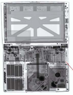
6 6 CMOS detector technology. Line scan cameras are simple to operate and integrate into a higher level inspection system. Their slim design allows installation of these cameras in a production line, underneath a conveyor belt (see Fig. 6). Figure 6: Exemplary configuration of an in-line x-ray inspection system These cameras capture images of objects on a conveyor by scanning the objects one line at a time as the conveyor moves. The lines are then stitched together by computer software to reconstruct the object s entire image. The line scan cameras require less radiation compared to a 2-D camera. The line sensor requires only a narrow beam of x-ray irradiation compared to 2-D cameras, which have a much larger area to be exposed. The reduced amount of radiation requires a simplified design and reduced space for the x-ray enclosure. Line scan cameras provide sufficient resolution for many inspection applications in the electronic industry. However there is a limit to spatial resolution these cameras typically have pixel sizes greater than 0.1 mm. An efficient AXI method which allows obtaining a higher resolution without compromising sensitivity is the method of x-ray TDI imaging. The x-ray TDI cameras provide sufficient resolution and sensitivity to inspect multilayer printed circuit boards, electronic assemblies with BGA and other surface-mounted components. They can detect solder bridges, open solder joints, insufficient or excess solder, voids, misregistrations, missing components, and other defects. These systems also allow visualizing the internal structure of electronic components, including the dies, wire bonds and other elements, and distinguishing the authentic components from counterfeit components. The Hamamatsu x-ray TDI camera (see Fig. 7) provides 292 mm detection width, scanning rate up to 2.1 KHz and 16 bit ADC (analog-to-digital conversion) resolution. This no-gap camera includes a TDI-CCD sensor with 48µm x 48µm pixels coupled to a fiber-optic plate with scintillator (FOS). The camera also includes analog and digital signal processing circuits, data output and control interfaces, and other electronic circuits. It can work with x-ray sources ranging from 25 kvp to 85 kvp. Figure 7: Hamamatsu x-ray TDI camera

7 7 AOI and AXI Applications The more effective integration time provided by TDI-CCD sensors makes them suitable for numerous AOI and AXI applications. In the semiconductor industry, manufacturers require wafer-auditing systems that can measure results of the layering, patterning, and doping processes for each layer. Time delay integration devices with gigapixel-per-second data rates have been used for wafer and reticle inspections in the semiconductor industry, wherein UV and DUV instruments must comply with defect detection requirements in deep-submicron microelectronics technologies. 5 Fig. 8 shows an example of optical inspection of a printed pattern. A Hamamatsu C10000 TDI-CCD camera was used for this experiment. Test conditions: optical magnification 30x, object speed 100 mm/s, line rate 40 khz. Figure 8: Optical inspection of a printed pattern An x-ray image of a PCB with SMT components taken with a Hamamatsu C10650 x-ray TDI camera is shown in Fig. 9. Figure 9: X-ray image of a PCB with SMT components Recently we have observed a growing interest in TDI linear sensors for 3-D x-ray inspection systems. It has been suggested that implementation of eight linear sensors would be considered a practical minimum for most inspection applications. 6
8 8 While any number of linear sensors may be employed to generate different viewing angles of the object being inspected, a range of twelve to sixteen linear sensors appears to generate a sufficient number of images for proper PCB inspection. In many cases, the use of more than sixteen linear sensors does not add significantly to the inspection capability. References As originally published in the IPC APEX EXPO Proceedings. 1. M. Muramatsu et al., Proceedings of SPIE 3019, 2-8 (April 1997). 2. G. C. Holst and T. S. Lomheim, CMOS/CCD Sensors and Camera systems, JCD Publishing and SPIE Press (2007). 3. J. Gilmore and Y. Bulayev, CCD advances improve TDI imaging techniques, Laser Focus World (January 2007). 4. A. Theuwissen, Time-delay and integration charge-coupled devices, Presentation at Hamamatsu Technology Seminar, San Diego, CA (June 6, 2008). 5. Semiconductor inspection relies on imaging, Vision Systems Design (March 2004). 6. G. L. Meyer, Precise x-ray inspection system utilizing multiple linear sensors, Patent No.: US 7,231,013 B2 (June 2007).
9 TDI Imaging: An Efficient AOI and AXI Tool Yakov Bulayev Hamamatsu Corporation Bridgewater, New Jersey
10 Introduction As a result of heightened requirements for product quality, integrity and reliability of electronic products, the role of wafer auditing and nondestructive testing of printed circuit boards and electronic assemblies has grown at an unprecedented rate It is estimated that the cost of a failure decreases by a factor of ten when the error is identified in the course of production instead of in the field Optical and x-ray TDI cameras have become one of the most efficient and reliable tools for nondestructive testing and inspection
11 Topics To Be Discussed Today Concepts of TDI imaging AOI applications AXI applications
12 Topics To Be Discussed Today Concepts of TDI imaging AOI applications AXI applications
13 TDI: Time Delay Integration TDI is an effective method for - Detection of low exposure levels - Clear imaging of moving objects By means of Accumulation of multiple exposures of the same object and noiseless integration of these exposures
14 Principle of TDI Operation
15 Signal-to-Noise Ratio Theoretically SNR TDI N SNR wherein N - number of TDI stages
16 Signal Integration in TDI System
17 Time Delay Integration Object TDI Imaging Output Image => Signal intensity TDI-CCD =>
18 TDI vs. Line Scan Camera Object Line Scan Camera TDI-CCD Camera
 TDI Line Rate < Object Velocity (10% Mismatch) TDI Line Rate << Object Velocity (~30% Mismatch)")
19 Scan-Velocity Mismatch TDI Line Rate = Object Velocity (No Mismatch) TDI Line Rate > Object Velocity (10% Mismatch) TDI Line Rate < Object Velocity (10% Mismatch) TDI Line Rate << Object Velocity (~30% Mismatch)
20 Topics To Be Discussed Today Concepts of TDI imaging AOI applications AXI applications

21 In-Line AOI System Conveyor Light Source TDI Camera
22 Spectral Response Characteristics Back-thinned CCD Front-illuminated CCD
23 Multitap TDI-CCD Sensor for Bidirectional Scanning


24 TDI Cameras for AOI Applications - 2K spatial resolution TDI stages - 12µm x 12 µm pixel size - Line rate up to 50 khz - 2K spatial resolution TDI stages - 12µm x 12 µm pixel size - Line rate up to 50 khz 4K spatial resolution -128 TDI stages -12µm x 12 µm pixel size - Line rate up to 100 khz

25 Optical Inspection Optical magnification: 30x Object speed: 100mm/s Line rate: 40kHz
26 Topics To Be Discussed Today Concepts of TDI imaging AOI applications AXI applications

27 AXI System X-ray source Object X-ray line scan camera


28 Line Scan Camera vs. 2-D Camera 2-D Camera Line Scan Camera

29 No-gap TDI Camera for AXI Applications - 292mm detection width - 6K spatial resolution TDI Stages - 48µm x 48µm pixel size - 25kVp to 85 kvp X-ray detection range - Line scan rate up to 2.1kHz

30 In-line AXI Setup Microfocus X-Ray Source Conveyor Line Scan Camera Electronic Assembly


31 X-ray Inspection (1) Geometrical magnification: 1x Line scan rate: 1.3kHz X-ray source: 110kV, 160µA
 Geometrical")


32 X-ray Inspection (2) Geometrical magnification: 1x Line scan rate: 1.3kHz X-ray source: 110kV, 160µA
33 X-ray Inspection (3)
34 Thank you! Copyright Hamamatsu Corporation
Image sensor combining the best of different worlds
 Image sensors and vision systems Image sensor combining the best of different worlds First multispectral time-delay-and-integration (TDI) image sensor based on CCD-in-CMOS technology. Introduction Jonathan
Detectors for microscopy - CCDs, APDs and PMTs. Antonia Göhler. Nov 2014
 Detectors for microscopy - CCDs, APDs and PMTs Antonia Göhler Nov 2014 Detectors/Sensors in general are devices that detect events or changes in quantities (intensities) and provide a corresponding output,
CCDS. Lesson I. Wednesday, August 29, 12
 CCDS Lesson I CCD OPERATION The predecessor of the CCD was a device called the BUCKET BRIGADE DEVICE developed at the Phillips Research Labs The BBD was an analog delay line, made up of capacitors such
Photons and solid state detection
 Photons and solid state detection Photons represent discrete packets ( quanta ) of optical energy Energy is hc/! (h: Planck s constant, c: speed of light,! : wavelength) For solid state detection, photons
IT FR R TDI CCD Image Sensor
 4k x 4k CCD sensor 4150 User manual v1.0 dtd. August 31, 2015 IT FR 08192 00 R TDI CCD Image Sensor Description: With the IT FR 08192 00 R sensor ANDANTA GmbH builds on and expands its line of proprietary
CCD Analogy BUCKETS (PIXELS) HORIZONTAL CONVEYOR BELT (SERIAL REGISTER) VERTICAL CONVEYOR BELTS (CCD COLUMNS) RAIN (PHOTONS)
 HORIZONTAL CONVEYOR BELT (SERIAL REGISTER) VERTICAL CONVEYOR BELTS (CCD COLUMNS) RAIN (PHOTONS)") CCD Analogy RAIN (PHOTONS) VERTICAL CONVEYOR BELTS (CCD COLUMNS) BUCKETS (PIXELS) HORIZONTAL CONVEYOR BELT (SERIAL REGISTER) MEASURING CYLINDER (OUTPUT AMPLIFIER) Exposure finished, buckets now contain
CCD Analogy RAIN (PHOTONS) VERTICAL CONVEYOR BELTS (CCD COLUMNS) BUCKETS (PIXELS) HORIZONTAL CONVEYOR BELT (SERIAL REGISTER) MEASURING CYLINDER (OUTPUT AMPLIFIER) Exposure finished, buckets now contain
Image acquisition. In both cases, the digital sensing element is one of the following: Line array Area array. Single sensor
 Image acquisition Digital images are acquired by direct digital acquisition (digital still/video cameras), or scanning material acquired as analog signals (slides, photographs, etc.). In both cases, the
Time Delay Integration (TDI), The Answer to Demands for Increasing Frame Rate/Sensitivity? Craige Palmer Assistant Sales Manager
, The Answer to Demands for Increasing Frame Rate/Sensitivity? Craige Palmer Assistant Sales Manager") Time Delay Integration (TDI), The Answer to Demands for Increasing Frame Rate/Sensitivity? Craige Palmer Assistant Sales Manager Laser Scanning Microscope High Speed Gated PMT Module High Speed Gating
Time Delay Integration (TDI), The Answer to Demands for Increasing Frame Rate/Sensitivity? Craige Palmer Assistant Sales Manager Laser Scanning Microscope High Speed Gated PMT Module High Speed Gating
EE 392B: Course Introduction
 EE 392B Course Introduction About EE392B Goals Topics Schedule Prerequisites Course Overview Digital Imaging System Image Sensor Architectures Nonidealities and Performance Measures Color Imaging Recent
Two-phase full-frame CCD with double ITO gate structure for increased sensitivity
 Two-phase full-frame CCD with double ITO gate structure for increased sensitivity William Des Jardin, Steve Kosman, Neal Kurfiss, James Johnson, David Losee, Gloria Putnam *, Anthony Tanbakuchi (Eastman
Amorphous Selenium Direct Radiography for Industrial Imaging
 DGZfP Proceedings BB 67-CD Paper 22 Computerized Tomography for Industrial Applications and Image Processing in Radiology March 15-17, 1999, Berlin, Germany Amorphous Selenium Direct Radiography for Industrial
CMOS X-RAY DETECTORS. for Industrial Non-Destructive Testing COMMITTED TO PEOPLE. DRIVEN BY INNOVATION.
 IMAGE SENSORS X-RAY DETECTORS IMAGE PROCESSING CUSTOM SOLUTIONS CMOS X-RAY DETECTORS for Industrial Non-Destructive Testing COMMITTED TO PEOPLE. DRIVEN BY INNOVATION. IMAGE SENSORS X-RAY DETECTORS IMAGE
brief history of photography foveon X3 imager technology description
 brief history of photography foveon X3 imager technology description imaging technology 30,000 BC chauvet-pont-d arc pinhole camera principle first described by Aristotle fourth century B.C. oldest known
Overview. Charge-coupled Devices. MOS capacitor. Charge-coupled devices. Charge-coupled devices:
 Overview Charge-coupled Devices Charge-coupled devices: MOS capacitors Charge transfer Architectures Color Limitations 1 2 Charge-coupled devices MOS capacitor The most popular image recording technology
VII. IR Arrays & Readout VIII.CCDs & Readout. This lecture course follows the textbook Detection of
 Detection of Light VII. IR Arrays & Readout VIII.CCDs & Readout This lecture course follows the textbook Detection of Light 4-3-2016 by George Rieke, Detection Cambridge of Light Bernhard Brandl University
Based on lectures by Bernhard Brandl
 Astronomische Waarneemtechnieken (Astronomical Observing Techniques) Based on lectures by Bernhard Brandl Lecture 10: Detectors 2 1. CCD Operation 2. CCD Data Reduction 3. CMOS devices 4. IR Arrays 5.
High-end CMOS Active Pixel Sensor for Hyperspectral Imaging
 R11 High-end CMOS Active Pixel Sensor for Hyperspectral Imaging J. Bogaerts (1), B. Dierickx (1), P. De Moor (2), D. Sabuncuoglu Tezcan (2), K. De Munck (2), C. Van Hoof (2) (1) Cypress FillFactory, Schaliënhoevedreef
Basler. Line Scan Cameras
 Basler Line Scan Cameras Next generation CMOS dual line scan technology Up to 140 khz at 2k or 4k resolution, up to 70 khz at 8k resolution Color line scan with 70 khz at 4k resolution High sensitivity
Improving the Collection Efficiency of Raman Scattering
 PERFORMANCE Unparalleled signal-to-noise ratio with diffraction-limited spectral and imaging resolution Deep-cooled CCD with excelon sensor technology Aberration-free optical design for uniform high resolution
Ultra-high resolution 14,400 pixel trilinear color image sensor
 Ultra-high resolution 14,400 pixel trilinear color image sensor Thomas Carducci, Antonio Ciccarelli, Brent Kecskemety Microelectronics Technology Division Eastman Kodak Company, Rochester, New York 14650-2008
Section 2: Lithography. Jaeger Chapter 2. EE143 Ali Javey Slide 5-1
 Section 2: Lithography Jaeger Chapter 2 EE143 Ali Javey Slide 5-1 The lithographic process EE143 Ali Javey Slide 5-2 Photolithographic Process (a) (b) (c) (d) (e) (f) (g) Substrate covered with silicon
Advanced Camera and Image Sensor Technology. Steve Kinney Imaging Professional Camera Link Chairman
 Advanced Camera and Image Sensor Technology Steve Kinney Imaging Professional Camera Link Chairman Content Physical model of a camera Definition of various parameters for EMVA1288 EMVA1288 and image quality
An Introduction to CCDs. The basic principles of CCD Imaging is explained.
 An Introduction to CCDs. The basic principles of CCD Imaging is explained. Morning Brain Teaser What is a CCD? Charge Coupled Devices (CCDs), invented in the 1970s as memory devices. They improved the
Lithography. 3 rd. lecture: introduction. Prof. Yosi Shacham-Diamand. Fall 2004
 Lithography 3 rd lecture: introduction Prof. Yosi Shacham-Diamand Fall 2004 1 List of content Fundamental principles Characteristics parameters Exposure systems 2 Fundamental principles Aerial Image Exposure
Tunable wideband infrared detector array for global space awareness
 Tunable wideband infrared detector array for global space awareness Jonathan R. Andrews 1, Sergio R. Restaino 1, Scott W. Teare 2, Sanjay Krishna 3, Mike Lenz 3, J.S. Brown 3, S.J. Lee 3, Christopher C.
Part I. CCD Image Sensors
 Part I CCD Image Sensors 2 Overview of CCD CCD is the abbreviation for charge-coupled device. CCD image sensors are silicon-based integrated circuits (ICs), consisting of a dense matrix of photodiodes
Charged Coupled Device (CCD) S.Vidhya
 S.Vidhya") Charged Coupled Device (CCD) S.Vidhya 02.04.2016 Sensor Physical phenomenon Sensor Measurement Output A sensor is a device that measures a physical quantity and converts it into a signal which can be read
Charged Coupled Device (CCD) S.Vidhya 02.04.2016 Sensor Physical phenomenon Sensor Measurement Output A sensor is a device that measures a physical quantity and converts it into a signal which can be read
Introduction. Chapter 16 Diagnostic Radiology. Primary radiological image. Primary radiological image
 Introduction Chapter 16 Diagnostic Radiology Radiation Dosimetry I Text: H.E Johns and J.R. Cunningham, The physics of radiology, 4 th ed. http://www.utoledo.edu/med/depts/radther In diagnostic radiology
CCD1600A Full Frame CCD Image Sensor x Element Image Area
 - 1 - General Description CCD1600A Full Frame CCD Image Sensor 10560 x 10560 Element Image Area General Description The CCD1600 is a 10560 x 10560 image element solid state Charge Coupled Device (CCD)
CCD Requirements for Digital Photography
 IS&T's 2 PICS Conference IS&T's 2 PICS Conference Copyright 2, IS&T CCD Requirements for Digital Photography Richard L. Baer Hewlett-Packard Laboratories Palo Alto, California Abstract The performance
STA1600LN x Element Image Area CCD Image Sensor
 ST600LN 10560 x 10560 Element Image Area CCD Image Sensor FEATURES 10560 x 10560 Photosite Full Frame CCD Array 9 m x 9 m Pixel 95.04mm x 95.04mm Image Area 100% Fill Factor Readout Noise 2e- at 50kHz
Characterisation of a CMOS Charge Transfer Device for TDI Imaging
 Preprint typeset in JINST style - HYPER VERSION Characterisation of a CMOS Charge Transfer Device for TDI Imaging J. Rushton a, A. Holland a, K. Stefanov a and F. Mayer b a Centre for Electronic Imaging,
BACKSIDE ILLUMINATED CMOS-TDI LINE SCANNER FOR SPACE APPLICATIONS
 BACKSIDE ILLUMINATED CMOS-TDI LINE SCANNER FOR SPACE APPLICATIONS O. Cohen, N. Ben-Ari, I. Nevo, N. Shiloah, G. Zohar, E. Kahanov, M. Brumer, G. Gershon, O. Ofer SemiConductor Devices (SCD) P.O.B. 2250,
Introduction. Chapter 1
 1 Chapter 1 Introduction During the last decade, imaging with semiconductor devices has been continuously replacing conventional photography in many areas. Among all the image sensors, the charge-coupled-device
X-ray light valve (XLV): a novel detectors technology for digital mammography*
: a novel detectors technology for digital mammography*") X-ray light valve (XLV): a novel detectors technology for digital mammography* Sorin Marcovici, Vlad Sukhovatkin, Peter Oakham XLV Diagnostics Inc., Thunder Bay, ON P7A 7T1, Canada ABSTRACT A novel method,
X-ray light valve (XLV): a novel detectors technology for digital mammography* Sorin Marcovici, Vlad Sukhovatkin, Peter Oakham XLV Diagnostics Inc., Thunder Bay, ON P7A 7T1, Canada ABSTRACT A novel method,
CMOS Today & Tomorrow
 CMOS Today & Tomorrow Uwe Pulsfort TDALSA Product & Application Support Overview Image Sensor Technology Today Typical Architectures Pixel, ADCs & Data Path Image Quality Image Sensor Technology Tomorrow
Copyright 2000 Society of Photo Instrumentation Engineers.
 Copyright 2000 Society of Photo Instrumentation Engineers. This paper was published in SPIE Proceedings, Volume 4043 and is made available as an electronic reprint with permission of SPIE. One print or
Section 2: Lithography. Jaeger Chapter 2 Litho Reader. The lithographic process
 Section 2: Lithography Jaeger Chapter 2 Litho Reader The lithographic process Photolithographic Process (a) (b) (c) (d) (e) (f) (g) Substrate covered with silicon dioxide barrier layer Positive photoresist
CHAPTER 9 POSITION SENSITIVE PHOTOMULTIPLIER TUBES
 CHAPTER 9 POSITION SENSITIVE PHOTOMULTIPLIER TUBES The current multiplication mechanism offered by dynodes makes photomultiplier tubes ideal for low-light-level measurement. As explained earlier, there
Digital Imaging Rochester Institute of Technology
 Digital Imaging 1999 Rochester Institute of Technology So Far... camera AgX film processing image AgX photographic film captures image formed by the optical elements (lens). Unfortunately, the processing
Cameras CS / ECE 181B
 Cameras CS / ECE 181B Image Formation Geometry of image formation (Camera models and calibration) Where? Radiometry of image formation How bright? What color? Examples of cameras What is a Camera? A camera
Receiver Performance and Comparison of Incoherent (bolometer) and Coherent (receiver) detection
 and Coherent (receiver) detection") At ev gap /h the photons have sufficient energy to break the Cooper pairs and the SIS performance degrades. Receiver Performance and Comparison of Incoherent (bolometer) and Coherent (receiver) detection
At ev gap /h the photons have sufficient energy to break the Cooper pairs and the SIS performance degrades. Receiver Performance and Comparison of Incoherent (bolometer) and Coherent (receiver) detection
Section 2: Lithography. Jaeger Chapter 2 Litho Reader. EE143 Ali Javey Slide 5-1
 Section 2: Lithography Jaeger Chapter 2 Litho Reader EE143 Ali Javey Slide 5-1 The lithographic process EE143 Ali Javey Slide 5-2 Photolithographic Process (a) (b) (c) (d) (e) (f) (g) Substrate covered
THE CCD RIDDLE REVISTED: SIGNAL VERSUS TIME LINEAR SIGNAL VERSUS VARIANCE NON-LINEAR
 THE CCD RIDDLE REVISTED: SIGNAL VERSUS TIME LINEAR SIGNAL VERSUS VARIANCE NON-LINEAR Mark Downing 1, Peter Sinclaire 1. 1 ESO, Karl Schwartzschild Strasse-2, 85748 Munich, Germany. ABSTRACT The photon
Digital Radiography : Flat Panel
 Digital Radiography : Flat Panel Flat panels performances & operation How does it work? - what is a sensor? - ideal sensor Flat panels limits and solutions - offset calibration - gain calibration - non
LENSES. INEL 6088 Computer Vision
 LENSES INEL 6088 Computer Vision Digital camera A digital camera replaces film with a sensor array Each cell in the array is a Charge Coupled Device light-sensitive diode that converts photons to electrons
How does prism technology help to achieve superior color image quality?
 WHITE PAPER How does prism technology help to achieve superior color image quality? Achieving superior image quality requires real and full color depth for every channel, improved color contrast and color
Image Formation and Capture. Acknowledgment: some figures by B. Curless, E. Hecht, W.J. Smith, B.K.P. Horn, and A. Theuwissen
 Image Formation and Capture Acknowledgment: some figures by B. Curless, E. Hecht, W.J. Smith, B.K.P. Horn, and A. Theuwissen Image Formation and Capture Real world Optics Sensor Devices Sources of Error
Lecture 20: Optical Tools for MEMS Imaging
 MECH 466 Microelectromechanical Systems University of Victoria Dept. of Mechanical Engineering Lecture 20: Optical Tools for MEMS Imaging 1 Overview Optical Microscopes Video Microscopes Scanning Electron
X-ray Imaging. PHYS Lecture. Carlos Vinhais. Departamento de Física Instituto Superior de Engenharia do Porto
 X-ray Imaging PHYS Lecture Carlos Vinhais Departamento de Física Instituto Superior de Engenharia do Porto cav@isep.ipp.pt Overview Projection Radiography Anode Angle Focal Spot Magnification Blurring
Properties of a Detector
 Properties of a Detector Quantum Efficiency fraction of photons detected wavelength and spatially dependent Dynamic Range difference between lowest and highest measurable flux Linearity detection rate
Submillimeter (continued)
") Submillimeter (continued) Dual Polarization, Sideband Separating Receiver Dual Mixer Unit The 12-m Receiver Here is where the receiver lives, at the telescope focus Receiver Performance T N (noise temperature)
Submillimeter (continued) Dual Polarization, Sideband Separating Receiver Dual Mixer Unit The 12-m Receiver Here is where the receiver lives, at the telescope focus Receiver Performance T N (noise temperature)
DEVELOPMENT CENTER X-RAY TECHNOLOGY EZRT XEYE. Radiation proof X-ray detectors for industrial applications
 DEVELOPMENT CENTER X-RAY TECHNOLOGY EZRT XEYE Radiation proof X-ray detectors for industrial applications The constantly high image quality and long service life of the digital X-ray detectors XEye developed
SATECH INC. The Solutions Provider!
 Quality Verification with Real-time X-ray By Richard Amtower One can look at trends in packaging and assembly and predict that geometries will continue to shrink and PCBs will become more complex. As a
Fundamentals of CMOS Image Sensors
 CHAPTER 2 Fundamentals of CMOS Image Sensors Mixed-Signal IC Design for Image Sensor 2-1 Outline Photoelectric Effect Photodetectors CMOS Image Sensor(CIS) Array Architecture CIS Peripherals Design Considerations
The new CMOS Tracking Camera used at the Zimmerwald Observatory
 13-0421 The new CMOS Tracking Camera used at the Zimmerwald Observatory M. Ploner, P. Lauber, M. Prohaska, P. Schlatter, J. Utzinger, T. Schildknecht, A. Jaeggi Astronomical Institute, University of Bern,
Introduction to Computer Vision
 Introduction to Computer Vision CS / ECE 181B Thursday, April 1, 2004 Course Details HW #0 and HW #1 are available. Course web site http://www.ece.ucsb.edu/~manj/cs181b Syllabus, schedule, lecture notes,
BF-X2. In-line 3D automated X-ray inspection system for Semiconductor, Power module inspection
 In-line automated X-ray inspection system for Semiconductor, Power module inspection BF-X2 Visualize the inner structure with innovative automated inspection In-line automated X-ray inspection system for
Last class. This class. CCDs Fancy CCDs. Camera specs scmos
 CCDs and scmos Last class CCDs Fancy CCDs This class Camera specs scmos Fancy CCD cameras: -Back thinned -> higher QE -Unexposed chip -> frame transfer -Electron multiplying -> higher SNR -Fancy ADC ->
A large format, high-performance CCD sensor for medical x-ray applications
 A large format, high-performance CCD sensor for medical x-ray applications William Des Jardin, Chris Parks, Hung Doan, Neal Kurfiss, and Keith Wetzel Eastman Kodak Company, Rochester, NY, 14650-2008 USA
PRELIMINARY. CCD 3041 Back-Illuminated 2K x 2K Full Frame CCD Image Sensor FEATURES
 CCD 3041 Back-Illuminated 2K x 2K Full Frame CCD Image Sensor FEATURES 2048 x 2048 Full Frame CCD 15 µm x 15 µm Pixel 30.72 mm x 30.72 mm Image Area 100% Fill Factor Back Illuminated Multi-Pinned Phase
RADIOGRAPHY TERMS TO KNOW SELF STUDY DENTALELLE TUTORING
 RADIOGRAPHY TERMS TO KNOW SELF STUDY DENTALELLE TUTORING PLEASE NOTE You DO NOT need to study these for the board exam if this is why you bought our Radiography course, however if you come across any terms
Engineering Medical Optics BME136/251 Winter 2018
 Engineering Medical Optics BME136/251 Winter 2018 Monday/Wednesday 2:00-3:20 p.m. Beckman Laser Institute Library, MSTB 214 (lab) *1/17 UPDATE Wednesday, 1/17 Optics and Photonic Devices III: homework
Digital Radiographic Inspection replacing traditional RT and 3D RT Development
 Digital Radiographic Inspection replacing traditional RT and 3D RT Development Iploca Novel Construction Meeting 27&28 March 2014 Geneva By Jan van der Ent Technical Authority International Contents Introduction
Image Sensor Characterization in a Photographic Context
 Image Sensor Characterization in a Photographic Context Sean C. Kelly, Gloria G. Putnam, Richard B. Wheeler, Shen Wang, William Davis, Ed Nelson, and Doug Carpenter Eastman Kodak Company Rochester, New
ME 6406 MACHINE VISION. Georgia Institute of Technology
 ME 6406 MACHINE VISION Georgia Institute of Technology Class Information Instructor Professor Kok-Meng Lee MARC 474 Office hours: Tues/Thurs 1:00-2:00 pm kokmeng.lee@me.gatech.edu (404)-894-7402 Class
Major Fabrication Steps in MOS Process Flow
 Major Fabrication Steps in MOS Process Flow UV light Mask oxygen Silicon dioxide photoresist exposed photoresist oxide Silicon substrate Oxidation (Field oxide) Photoresist Coating Mask-Wafer Alignment
light sensing & sensors Mo: Tu:04 light sensing & sensors 167+1
 light sensing & sensors 16722 mws@cmu.edu Mo:20090302+Tu:04 light sensing & sensors 167+1 reading Fraden Section 3.13, Light, and Chapter 14, Light Detectors 16722 mws@cmu.edu Mo:20090302+Tu:04 light sensing
Fully depleted, thick, monolithic CMOS pixels with high quantum efficiency
 Fully depleted, thick, monolithic CMOS pixels with high quantum efficiency Andrew Clarke a*, Konstantin Stefanov a, Nicholas Johnston a and Andrew Holland a a Centre for Electronic Imaging, The Open University,
Lecture Notes 10 Image Sensor Optics. Imaging optics. Pixel optics. Microlens
 Lecture Notes 10 Image Sensor Optics Imaging optics Space-invariant model Space-varying model Pixel optics Transmission Vignetting Microlens EE 392B: Image Sensor Optics 10-1 Image Sensor Optics Microlens
An Introduction to Scientific Imaging C h a r g e - C o u p l e d D e v i c e s
 p a g e 2 S C I E N T I F I C I M A G I N G T E C H N O L O G I E S, I N C. Introduction to the CCD F u n d a m e n t a l s The CCD Imaging A r r a y An Introduction to Scientific Imaging C h a r g e -
WHITE PAPER. Sensor Comparison: Are All IMXs Equal? Contents. 1. The sensors in the Pregius series
 WHITE PAPER www.baslerweb.com Comparison: Are All IMXs Equal? There have been many reports about the Sony Pregius sensors in recent months. The goal of this White Paper is to show what lies behind the
The Charge-Coupled Device. Many overheads courtesy of Simon Tulloch
 The Charge-Coupled Device Astronomy 1263 Many overheads courtesy of Simon Tulloch smt@ing.iac.es Jan 24, 2013 What does a CCD Look Like? The fine surface electrode structure of a thick CCD is clearly visible
Chromatic X-Ray imaging with a fine pitch CdTe sensor coupled to a large area photon counting pixel ASIC
 Chromatic X-Ray imaging with a fine pitch CdTe sensor coupled to a large area photon counting pixel ASIC R. Bellazzini a,b, G. Spandre a*, A. Brez a, M. Minuti a, M. Pinchera a and P. Mozzo b a INFN Pisa
In the name of God, the most merciful Electromagnetic Radiation Measurement
 In the name of God, the most merciful Electromagnetic Radiation Measurement In these slides, many figures have been taken from the Internet during my search in Google. Due to the lack of space and diversity
Strip Detectors. Principal: Silicon strip detector. Ingrid--MariaGregor,SemiconductorsasParticleDetectors. metallization (Al) p +--strips
 p +--strips") Strip Detectors First detector devices using the lithographic capabilities of microelectronics First Silicon detectors -- > strip detectors Can be found in all high energy physics experiments of the last
Strip Detectors First detector devices using the lithographic capabilities of microelectronics First Silicon detectors -- > strip detectors Can be found in all high energy physics experiments of the last
Observational Astronomy
 Observational Astronomy Instruments The telescope- instruments combination forms a tightly coupled system: Telescope = collecting photons and forming an image Instruments = registering and analyzing the
Hiding In Plain Sight. How Ultrasonics Can Help You Find the Smallest Bonded Wafer and Device Defects. A Sonix White Paper
 Hiding In Plain Sight How Ultrasonics Can Help You Find the Smallest Bonded Wafer and Device Defects A Sonix White Paper If You Can See It, You Can Solve It: Understanding Ultrasonic Inspection of Bonded
Three Ways to Detect Light. We now establish terminology for photon detectors:
 Three Ways to Detect Light In photon detectors, the light interacts with the detector material to produce free charge carriers photon-by-photon. The resulting miniscule electrical currents are amplified
OCT Spectrometer Design Understanding roll-off to achieve the clearest images
 OCT Spectrometer Design Understanding roll-off to achieve the clearest images Building a high-performance spectrometer for OCT imaging requires a deep understanding of the finer points of both OCT theory
Advances in X-Ray Technology for Semicon Applications Keith Bryant and Thorsten Rother
 Advances in X-Ray Technology for Semicon Applications Keith Bryant and Thorsten Rother X-Ray Champions, Telspec, Yxlon International Agenda The x-ray tube, the heart of the system Advances in digital detectors
Instruction manual and data sheet ipca h
 1/15 instruction manual ipca-21-05-1000-800-h Instruction manual and data sheet ipca-21-05-1000-800-h Broad area interdigital photoconductive THz antenna with microlens array and hyperhemispherical silicon
More Imaging Luc De Mey - CEO - CMOSIS SA
 More Imaging Luc De Mey - CEO - CMOSIS SA Annual Review / June 28, 2011 More Imaging CMOSIS: Vision & Mission CMOSIS s Business Concept On-Going R&D: More Imaging CMOSIS s Vision Image capture is a key
Evaluating Commercial Scanners for Astronomical Images. The underlying technology of the scanners: Pixel sizes:
 Evaluating Commercial Scanners for Astronomical Images Robert J. Simcoe Associate Harvard College Observatory rjsimcoe@cfa.harvard.edu Introduction: Many organizations have expressed interest in using
Vision Lighting Seminar
 Creators of Evenlite Vision Lighting Seminar Daryl Martin Midwest Sales & Support Manager Advanced illumination 734-213 213-13121312 dmartin@advill.com www.advill.com 2005 1 Objectives Lighting Source
Integrated Multi-Aperture Imaging
 Integrated Multi-Aperture Imaging Keith Fife, Abbas El Gamal, Philip Wong Department of Electrical Engineering, Stanford University, Stanford, CA 94305 1 Camera History 2 Camera History Despite progress,
3D light microscopy techniques
 3D light microscopy techniques The image of a point is a 3D feature In-focus image Out-of-focus image The image of a point is not a point Point Spread Function (PSF) 1D imaging 2D imaging 3D imaging Resolution
Image Formation and Camera Design
 Image Formation and Camera Design Spring 2003 CMSC 426 Jan Neumann 2/20/03 Light is all around us! From London & Upton, Photography Conventional camera design... Ken Kay, 1969 in Light & Film, TimeLife
Real Time Linear Array Imaging. Brian Caccamise
 Real Time Linear Array Imaging Brian Caccamise 1 Real Time Linear Array Imaging What is Real Time Linear Array Imaging? Or Real Time Radiography (RTR)? 2 Real Time Linear Array Imaging It s Not This! Shoe
Backside illuminated CMOS-TDI line scan sensor for space applications
 Backside illuminated CMOS-TDI line scan sensor for space applications Omer COHEN, Oren OFER, Gil ABRAMOVICH, Nimrod BEN-ARI, Gal GERSHON, Maya BRUMER, Adi SHAY, Yaron SHAMAY SemiConductor Devices (SCD)
Simulation of High Resistivity (CMOS) Pixels
 Pixels") Simulation of High Resistivity (CMOS) Pixels Stefan Lauxtermann, Kadri Vural Sensor Creations Inc. AIDA-2020 CMOS Simulation Workshop May 13 th 2016 OUTLINE 1. Definition of High Resistivity Pixel Also
Simulation of High Resistivity (CMOS) Pixels Stefan Lauxtermann, Kadri Vural Sensor Creations Inc. AIDA-2020 CMOS Simulation Workshop May 13 th 2016 OUTLINE 1. Definition of High Resistivity Pixel Also
Light gathering Power: Magnification with eyepiece:
 Telescopes Light gathering Power: The amount of light that can be gathered by a telescope in a given amount of time: t 1 /t 2 = (D 2 /D 1 ) 2 The larger the diameter the smaller the amount of time. If
the need for an intensifier
 * The LLLCCD : Low Light Imaging without the need for an intensifier Paul Jerram, Peter Pool, Ray Bell, David Burt, Steve Bowring, Simon Spencer, Mike Hazelwood, Ian Moody, Neil Catlett, Philip Heyes Marconi
Applications of Steady-state Multichannel Spectroscopy in the Visible and NIR Spectral Region
 Feature Article JY Division I nformation Optical Spectroscopy Applications of Steady-state Multichannel Spectroscopy in the Visible and NIR Spectral Region Raymond Pini, Salvatore Atzeni Abstract Multichannel
Lecture 18: Photodetectors
 Lecture 18: Photodetectors Contents 1 Introduction 1 2 Photodetector principle 2 3 Photoconductor 4 4 Photodiodes 6 4.1 Heterojunction photodiode.................... 8 4.2 Metal-semiconductor photodiode................
Components of Optical Instruments 1
 Components of Optical Instruments 1 Optical phenomena used for spectroscopic methods: (1) absorption (2) fluorescence (3) phosphorescence (4) scattering (5) emission (6) chemiluminescence Spectroscopic
Charged-Coupled Devices
 Charged-Coupled Devices Charged-Coupled Devices Useful texts: Handbook of CCD Astronomy Steve Howell- Chapters 2, 3, 4.4 Measuring the Universe George Rieke - 3.1-3.3, 3.6 CCDs CCDs were invented in 1969
Applications for cameras with CMOS-, CCD- and InGaAssensors. Jürgen Bretschneider AVT, 2014
 Applications for cameras with CMOS-, CCD- and InGaAssensors Jürgen Bretschneider AVT, 2014 Allied Vision Technologies Profile Foundation: 1989,Headquarters: Stadtroda (Thüringen), Employees: aprox. 265
Image Formation and Capture
 Figure credits: B. Curless, E. Hecht, W.J. Smith, B.K.P. Horn, A. Theuwissen, and J. Malik Image Formation and Capture COS 429: Computer Vision Image Formation and Capture Real world Optics Sensor Devices
3D light microscopy techniques
 3D light microscopy techniques The image of a point is a 3D feature In-focus image Out-of-focus image The image of a point is not a point Point Spread Function (PSF) 1D imaging 1 1 2! NA = 0.5! NA 2D imaging