Considerations for Capacitor Selection in FPGA Designs CARTS 2005
|
|
|
- Maximillian Parker
- 6 years ago
- Views:
Transcription
1 Considerations for Capacitor Selection in FPGA Designs CARTS 2005 Steve Weir Teraspeed Consulting Group LLC Page 1
2 Agenda What does an FPGA power delivery system look like? What really matters in a FPGA PDS? Do low inductance capacitors help? Comparisons of low inductance capacitors for power bypass applications. Conclusions Page 2
3 FPGA Power Delivery Systems Power / ground planes model as meshed transmission lines Page 3
4 FPGA Power Delivery Systems Voltage regulator module attaches into the mesh, whether bulk or point-of-load Page 4
5 FPGA Power Delivery Systems Bypass capacitors locate at various points in the grid. Page 5
6 FPGA Power Delivery Systems FPGA mount and package, form a low-pass filter that limits HF current flow. Usually less than 50MHz This frequency range is ( FORTUNATELY! ) within the range of discrete ceramic capacitors. Page 6
7 Bypass Significance to High-Speed Signal Returns Properly routed high speed signals reference a single voltage rail Properly routed high-speed signals DO NOT TRAVERSE the bypass network to switch routing layers! Properly routed high-speed signals DO NOT TRAVERSE plane cavity capacitance to switch routing layers! Page 7
8 FPGA Signal Propagation Older Packages Page 8
9 FPGA Signal Propagation New Packages Page 9
10 Parasitics, FPGA to Bypass Caps Page 10

11 PCB Inductance For simple power / ground patterns, spreading inductance may be readily determined by application of the Biot-Savart law. Radial spreading inductance: Page 11

12 Spreading Inductance Limits on Capacitor Effectiveness Capacitor incremental effectiveness drops rapidly Page 12

13 Capacitor Attachment Via Inductance For vias contained within plane cavities, inductance varies linearly with height. Page 13
14 The Dark Side of Vias: Perforate the planes, Luke Vias are a necessary but expensive part of power interconnect. Extra vias cause extra: Plane perforation- Increased plane spreading impedance Degradation of signal return path Blocked signal routes- Alternatives: blind vias or more layers are expensive Direct drilling costs- Vias at $0.005/hole / $0.01 / capacitor typical, often COST MORE than the capacitors they connect! VIA utilization is an important system cost factor. Page 14
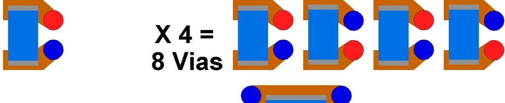
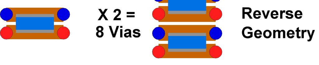
15 Current Gen. Low L Caps Reverse geometry capacitors: 0612, 0508, 0306, etc. AVX Corp. IDC capacitors 0612, 0508 Array capacitors 0612, 0508 X2Y capacitors 1206 ( and larger ), 0805, 0603 Page 15
16 Reverse Geometry Capacitors Interconnect on long axis Induction loop across short axis Best, low-inductance attachment is at device ends. Yields two capacitors each w/ X-Y plane induction loop about ½ of traditional cap. Can replace two to four regular caps depending on via and plane geometries Page 16

17 Reverse Geometry Capacitors Optimum via arrangement emulates two smaller geometry capacitors. IE 2 X 0303 for 0306 parts Page 17


18 AVX Corp. IDC Capacitors Major improvement of reverse geometry concept: Typically eight attachment terminals Terminals interleave polarity to reduce BOTH via and device inductance Eight terminal devices form SIX SMALL X-Y plane induction loops Page 18

19 AVX Corp. IDC Capacitors Page 19
20 AVX Corp. IDC Capacitors Via utilization affected by current crowding in the center vias and terminals. For eight terminal device, ideal via K factor would be 0.250, is 0.333, +33%. Can replace from three to six+ regular caps depending on via and plane geometries 4:1 5.5:1 typical, with proper placement Page 20

21 Array Capacitors Four independent capacitors in parallel. Can be wired interdigitated like an IDC Induction loops are hybrid of six X-Y loops of IDC for the vias, and four loops across device short axis Do not perform as well as IDC s, BUT Exhibit more even current distribution than IDC s Can replace from three+ to four regular caps Not an IDC, but not bad for moderate performance applications. Page 21


22 Array Capacitors When wired in parallel, perform poorly. Vias form solenoid like magnetic structure When wired like an IDC, via induction is similar to IDC, but cap induction is much worse. Page 22
23 The X2Y Capacitor Instead of reverse geometry, the X2Y is a perpendicular geometry capacitor. X-Y plane current loops form around each corner. Current distribution is extraordinarily even in large devices where eight vias may be used well Current distribution has similar asymmetry as IDC devices for smaller ( < 1206 ) devices Six terminal attach K = vs ideal, +13% Page 23

24 The X2Y Capacitor Page 24
25 The X2Y Capacitor 0603 X2Y is smallest size low L cap Can replace from three to six+ regular caps depending on via and plane geometries 4:1 5.5:1 typical, with proper placement Performance of six via 0603 X2Y essentially identical to eight via IDC 0612 or 0508 X-Y induction across corners for X2Y result in negligible increase in inductance in larger X2Y caps X2Y 2220 inductance actually LOWER than X2Y 0603 X2Y 2220 w/eight vias, lowest mounted L of any ceramic cap Page 25
26 Capacitor Array Effects The Dark Side of Vias, Reduxe Low impedance systems require the equivalent of many conventional, two terminal MLCC caps. When placed in close proximity, mutual inductance between adjacent capacitors dilutes the benefit of each. IE, two capacitors exhibit mounted L much greater than ½ the mounted L of just one capacitor. Example measurements on a four layer board: mounted in isolation: 1700pH mounted in array w/interdigitated power / gnd vias: 620pH, 45% higher than 425pH ideal. Page 26

27 Cap and Via Count Comparisons IDC and X2Y yield lowest capacitor counts IDC increases via count over conventional caps significantly for low performance supplies, ie long vias. X2Y yields lowest via count Page 27


28 PCB Area Comparison Page 28


29 Practical Example Virtex2 FFBGA ea X2Y xfer Z <= 104 ea pwr / gnd ring Page 29


30 Practical Example Virtex2 FFBGA ea X2Y Xfer Z << 104 ea 0402 Additional advantage for Virtex4 and similar Page 30
31 Page 31 Conclusions Low inductance capacitors are becoming increasingly important to FPGA PDS designs Drill and placement costs dominate capacitor system cost REDUCE COMPONENT COUNT! REDUCE VIA COUNTS! As capacitor counts rise, incremental effectiveness diminishes X2Y capacitors offer the lowest in-system: Mounted inductance Component count Via count Real estate consumption
Webinar: Suppressing BGAs and/or multiple DC rails Keith Armstrong. 1of 5
 1of 5 Suppressing ICs with BGA packages and multiple DC rails Some Intel Core i5 BGA packages CEng, EurIng, FIET, Senior MIEEE, ACGI Presenter Contact Info email: keith.armstrong@cherryclough.com website:
Power Distribution Network Design for Stratix IV GX and Arria II GX FPGAs
 Power Distribution Network Design for Stratix IV GX and Arria II GX FPGAs Transceiver Portfolio Workshops 2009 Question What is Your PDN Design Methodology? Easy Complex Historical Full SPICE simulation
Decoupling capacitor placement
 Decoupling capacitor placement Covered in this topic: Introduction Which locations need decoupling caps? IC decoupling Capacitor lumped model How to maximize the effectiveness of a decoupling cap Parallel
AN4819 Application note
 Application note PCB design guidelines for the BlueNRG-1 device Introduction The BlueNRG1 is a very low power Bluetooth low energy (BLE) single-mode system-on-chip compliant with Bluetooth specification
The Quantitative Measurement of the Effectiveness of Decoupling Capacitors in Controlling Switching Transients from Microprocessors
 The Quantitative Measurement of the Effectiveness of Decoupling Capacitors in Controlling Switching Transients from Microprocessors Dale L. Sanders X2Y Attenuators, LLC 37554 Hills Tech Dr. Farmington
PDN Application of Ferrite Beads
 PDN Application of Ferrite Beads 11 TA3 Steve Weir CTO IPBLOX, LLC 1 Objectives Understand ferrite beads with a good model Understand PDN design w/ sensitive loads Understand how to determine when a ferrite
Mutual Coupling between Two Patches using Ideal High Impedance Surface
 International Journal of Electronics and Communication Engineering. ISSN 0974-2166 Volume 4, Number 3 (2011), pp. 287-293 International Research Publication House http://www.irphouse.com Mutual Coupling
IC Decoupling and EMI Suppression using X2Y Technology
 IC Decoupling and EMI Suppression using X2Y Technology Summary Decoupling and EMI suppression of ICs is a complex system level engineering problem complicated by the desire for faster switching gates,
A Solution to Simplify 60A Multiphase Designs By John Lambert & Chris Bull, International Rectifier, USA
 A Solution to Simplify 60A Multiphase Designs By John Lambert & Chris Bull, International Rectifier, USA As presented at PCIM 2001 Today s servers and high-end desktop computer CPUs require peak currents
Land Grid Array (LGA) Low Inductance Capacitor Advantages in Military and Aerospace Applications
 Low Inductance Capacitor Advantages in Military and Aerospace Applications") Land Grid Array (LGA) Low Inductance Capacitor Advantages in Military and Aerospace Applications A B S T R A C T : The benefits of Land Grid Array (LGA) capacitors and superior low inductance performance
Land Grid Array (LGA) Low Inductance Capacitor Advantages in Military and Aerospace Applications A B S T R A C T : The benefits of Land Grid Array (LGA) capacitors and superior low inductance performance
Physically-Based Distributed Models for Multi-Layer Ceramic Capacitors
 Physically-Based Distributed Models for Multi-Layer Ceramic Capacitors Charles R Sullivan and Yuqin Sun Thayer School of Engineering Dartmouth College http://power.thayer.dartmouth.edu/ Introduction Why
DesignCon Panel discussion: What is New in DC-DC Converters? V. Joseph Thottuvelil GE Energy Chris Young Intersil Zilker Labs
 DesignCon 2012 Panel discussion: What is New in DC-DC Converters? Panelists: V. Joseph Thottuvelil GE Energy Chris Young Intersil Zilker Labs Steve Weir IPBLOX Istvan Novak* Oracle * panel organizer and
The Inductance Loop Power Distribution in the Semiconductor Test Interface. Jason Mroczkowski Multitest
 The Inductance Loop Power Distribution in the Semiconductor Test Interface Jason Mroczkowski Multitest j.mroczkowski@multitest.com Silicon Valley Test Conference 2010 1 Agenda Introduction to Power Delivery
Measurement and Comparative S21 Performance of Raw and Mounted Decoupling Capacitors
 Measurement and Comparative S21 Performance of Raw and Mounted Decoupling Capacitors Summary Introduction Capacitors All IC power systems require some level of passive decoupling. The ability to accurately
Decoupling capacitor uses and selection
 Decoupling capacitor uses and selection Proper Decoupling Poor Decoupling Introduction Covered in this topic: 3 different uses of decoupling capacitors Why we need decoupling capacitors Power supply rail
What is New about Thin Laminates in 2013?
 PCBDesign 007 QuietPower column What is New about Thin Laminates in 2013? Istvan Novak, Oracle, February 2013 It is almost two years ago that the QuietPower column Thin Laminates: Buried Capacitance or
Chapter 16 PCB Layout and Stackup
 Chapter 16 PCB Layout and Stackup Electromagnetic Compatibility Engineering by Henry W. Ott Foreword The PCB represents the physical implementation of the schematic. The proper design and layout of a printed
Passive Components around ADAS Applications By Ron Demcko, AVX Fellow, AVX Corporation
 Passive Components around ADAS Applications By Ron Demcko, AVX Fellow, AVX Corporation The importance of high reliability - high performance electronics is accelerating as Advanced Driver Assistance Systems
Texas Instruments DisplayPort Design Guide
 Texas Instruments DisplayPort Design Guide April 2009 1 High Speed Interface Applications Introduction This application note presents design guidelines, helping users of Texas Instruments DisplayPort devices
Internal Model of X2Y Chip Technology
 Internal Model of X2Y Chip Technology Summary At high frequencies, traditional discrete components are significantly limited in performance by their parasitics, which are inherent in the design. For example,
Frequency-Domain Characterization of Power Distribution Networks
 Frequency-Domain Characterization of Power Distribution Networks Istvan Novak Jason R. Miller ARTECH H O U S E BOSTON LONDON artechhouse.com Preface Acknowledgments xi xv CHAPTER 1 Introduction 1 1.1 Evolution
High Performance ZVS Buck Regulator Removes Barriers To Increased Power Throughput In Wide Input Range Point-Of-Load Applications
 WHITE PAPER High Performance ZVS Buck Regulator Removes Barriers To Increased Power Throughput In Wide Input Range Point-Of-Load Applications Written by: C. R. Swartz Principal Engineer, Picor Semiconductor
X2Y Capacitors for Instrumentation Amplifier RFI Suppression
 XY Capacitors for Instrumentation mplifier Summary Instrumentation amplifiers are often employed in hostile environments. Long sensor lead cables may pick-up substantial RF radiation, particularly if they
CHAPTER 8 ANTENNAS 1
 CHAPTER 8 ANTENNAS 1 2 Antennas A good antenna works A bad antenna is a waste of time & money Antenna systems can be very inexpensive and simple They can also be very expensive 3 Antenna Considerations
Cyclone III Simultaneous Switching Noise (SSN) Design Guidelines
 Design Guidelines") Cyclone III Simultaneous Switching Noise (SSN) Design Guidelines December 2007, ver. 1.0 Introduction Application Note 508 Low-cost FPGAs designed on 90-nm and 65-nm process technologies are made to support
Cyclone III Simultaneous Switching Noise (SSN) Design Guidelines December 2007, ver. 1.0 Introduction Application Note 508 Low-cost FPGAs designed on 90-nm and 65-nm process technologies are made to support
Class-D Audio Power Amplifiers: PCB Layout For Audio Quality, EMC & Thermal Success (Home Entertainment Devices)
") Class-D Audio Power Amplifiers: PCB Layout For Audio Quality, EMC & Thermal Success (Home Entertainment Devices) Stephen Crump http://e2e.ti.com Audio Power Amplifier Applications Audio and Imaging Products
Class-D Audio Power Amplifiers: PCB Layout For Audio Quality, EMC & Thermal Success (Home Entertainment Devices) Stephen Crump http://e2e.ti.com Audio Power Amplifier Applications Audio and Imaging Products
Today I would like to present a short introduction to microstrip cross-coupled filter design. I will be using Sonnet em to analyze my planar circuit.
 Today I would like to present a short introduction to microstrip cross-coupled filter design. I will be using Sonnet em to analyze my planar circuit. And I will be using our optimizer, EQR_OPT_MWO, in
Presented by: Jim P. Muccioli
 Dale L. Sanders X2Y Attenuators, LLC 37554 Hills Tech Dr. Farmington Hills, MI 48331 James P. Muccioli X2Y Attenuators, LLC 37554 Hills Tech Dr. Farmington Hills, MI 48331 Terry M. North DiamlerChrysler
X2Y versus CM Chokes and PI Filters. Content X2Y Attenuators, LLC
 X2Y versus CM Chokes and PI Filters 1 Common Mode and EMI Most EMI compliance problems are common mode emissions. Only 10 s of uas in external cables are enough to violate EMC standards. 2 Common Mode
Intel 82566/82562V Layout Checklist (version 1.0)
") Intel 82566/82562V Layout Checklist (version 1.0) Project Name Fab Revision Date Designer Intel Contact SECTION CHECK ITEMS REMARKS DONE General Ethernet Controller Obtain the most recent product documentation
Intel 82566/82562V Layout Checklist (version 1.0) Project Name Fab Revision Date Designer Intel Contact SECTION CHECK ITEMS REMARKS DONE General Ethernet Controller Obtain the most recent product documentation
Technology in Balance
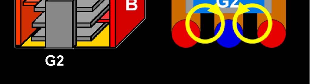
 Technology in Balance A G1 G2 B Basic Structure Comparison Regular capacitors have two plates or electrodes surrounded by a dielectric material. There is capacitance between the two conductive plates within
On-Chip Inductance Modeling
 On-Chip Inductance Modeling David Blaauw Kaushik Gala ladimir Zolotov Rajendran Panda Junfeng Wang Motorola Inc., Austin TX 78729 ABSTRACT With operating frequencies approaching the gigahertz range, inductance
Analysis and Reduction of On-Chip Inductance Effects in Power Supply Grids
 Analysis and Reduction of On-Chip Inductance Effects in Power Supply Grids Woo Hyung Lee Sanjay Pant David Blaauw Department of Electrical Engineering and Computer Science {leewh, spant, blaauw}@umich.edu
Broadband Methodology for Power Distribution System Analysis of Chip, Package and Board for High Speed IO Design
 DesignCon 2009 Broadband Methodology for Power Distribution System Analysis of Chip, Package and Board for High Speed IO Design Hsing-Chou Hsu, VIA Technologies jimmyhsu@via.com.tw Jack Lin, Sigrity Inc.
Controlling Input Ripple and Noise in Buck Converters
 Controlling Input Ripple and Noise in Buck Converters Using Basic Filtering Techniques, Designers Can Attenuate These Characteristics and Maximize Performance By Charles Coles, Advanced Analogic Technologies,
LP3120. White LED Backlighting Li-Ion Battery Backup Supplies Local 3V to 5V Conversion Smart Card Readers PCMCIA Local 5V Supplies
 http://www.szczkjgs.com LP3120 Low Noise, Regulated Charge Pump DC/DC Converter Features Fixed 5V ± 4% Output VIN Range: 2.5V to 5V Output Current: Up to 250mA Constant Frequency Operation at All Loads
A Simulation Study of Simultaneous Switching Noise
 A Simulation Study of Simultaneous Switching Noise Chi-Te Chen 1, Jin Zhao 2, Qinglun Chen 1 1 Intel Corporation Network Communication Group, LOC4/19, 9750 Goethe Road, Sacramento, CA 95827 Tel: 916-854-1178,
EL7302. Hardware Design Guide
 Hardware Design Guide Version: Preliminary 0.0 Date: January. 2005 Approval: Etron technology, Inc P.O. Box 19-54 No.6 Technology Road V. Science-based Industrial Park, Hsinchu,30077 Taiwan, R.O.C. Tel:
PI3DPX1207B Layout Guideline. Table of Contents. 1 Layout Design Guideline Power and GROUND High-speed Signal Routing...
 PI3DPX1207B Layout Guideline Table of Contents 1 Layout Design Guideline... 2 1.1 Power and GROUND... 2 1.2 High-speed Signal Routing... 3 2 PI3DPX1207B EVB layout... 8 3 Related Reference... 8 Page 1
March 6-9, 2016 Hilton Phoenix / Mesa Hotel Mesa, Arizona Archive- Session 4
 Proceedings Archive March 6-9, 2016 Hilton Phoenix / Mesa Hotel Mesa, Arizona Archive- Session 4 2016 BiTS Workshop Image: Stiop / Dollarphotoclub Proceedings Archive Presentation / Copyright Notice The
Dr. P. C. Pandey. EE Dept, IIT Bombay. Rev. Jan 16
 1 PCB DESIGN Dr. P. C. Pandey EE Dept, IIT Bombay Rev. Jan 16 2 Topics 1.General Considerations in Layout Design 2.Layout Design for Analog Circuits 3.Layout Design for Digital Circuits 4. Artwork Considerations
Lab Hints. How to reduce the degree of effort in testing lab assignments GENERAL WIRING PARASITICS... 2 OSCILLATION... 3
 Lab Hints How to reduce the degree of effort in testing lab assignments GENERAL WIRING PARASITICS... 2 OSCILLATION... 3 COUPLING & OSCILLATION DUE TO SLOPPY WIRING ON THE BENCH... 3 SHARING OF GROUND CONNECTIONS
ThinPAK 8x8. New High Voltage SMD-Package. April 2010 Version 1.0
 ThinPAK 8x8 New High Voltage SMD-Package Version 1.0 Content Introduction Package Specification Thermal Concept Application Test Conditions Impact on Efficiency and EMI Switching behaviour Portfolio and
Tag Designs and Techniques Used in HF RFID Item Level Tracking
 Tag Designs and Techniques Used in HF RFID Item Level Tracking The choice and placement of a RFID 1 tag on a product requires an investigation to determine optimal performance. Tags come in many sizes
Suppression Techniques using X2Y as a Broadband EMI Filter IEEE International Symposium on EMC, Boston, MA
 Suppression Techniques using X2Y as a Broadband EMI Filter Jim Muccioli Tony Anthony Dave Anthony Dale Sanders X2Y Attenuators, LLC Erie, PA 16506-2972 www.x2y.com Email: x2y@x2y.com Bart Bouma Yageo/Phycomp
The number of layers The number and types of planes (power and/or ground) The ordering or sequence of the layers The spacing between the layers
 The ordering or sequence of the layers The spacing between the layers") PCB Layer Stackup PCB layer stackup (the ordering of the layers and the layer spacing) is an important factor in determining the EMC performance of a product. The following four factors are important with
PCB Layer Stackup PCB layer stackup (the ordering of the layers and the layer spacing) is an important factor in determining the EMC performance of a product. The following four factors are important with
Understanding, measuring, and reducing output noise in DC/DC switching regulators
 Understanding, measuring, and reducing output noise in DC/DC switching regulators Practical tips for output noise reduction Katelyn Wiggenhorn, Applications Engineer, Buck Switching Regulators Robert Blattner,
Relationship Between Signal Integrity and EMC
 Relationship Between Signal Integrity and EMC Presented by Hasnain Syed Solectron USA, Inc. RTP, North Carolina Email: HasnainSyed@solectron.com 06/05/2007 Hasnain Syed 1 What is Signal Integrity (SI)?
Real World Application of Filtering
 Real World Application of Filtering COPYRIGHT NOTICE: JASTECH EMC CONSULTING, LLC 2001 reproduction or translation in any form of any part of this work is prohibited unless written permission is obtained
Learning the Curve BEYOND DESIGN. by Barry Olney
 by Barry Olney coulmn BEYOND DESIGN Learning the Curve Currently, power integrity is just entering the mainstream market phase of the technology adoption life cycle. The early market is dominated by innovators
Improving the immunity of sensitive analogue electronics
 Improving the immunity of sensitive analogue electronics T.P.Jarvis BSc CEng MIEE MIEEE, I.R.Marriott BEng, EMC Journal 1997 Introduction The art of good analogue electronics design has appeared to decline
Application of Generalized Scattering Matrix for Prediction of Power Supply Noise
 Application of Generalized Scattering Matrix for Prediction of Power Supply Noise System Level Interconnect Prediction 2010 June 13, 2010 K. Yamanaga (1),K. Masu (2), and T. Sato (3) (1) Murata Manufacturing
EC6011-ELECTROMAGNETICINTERFERENCEANDCOMPATIBILITY
 EC6011-ELECTROMAGNETICINTERFERENCEANDCOMPATIBILITY UNIT-3 Part A 1. What is an opto-isolator? [N/D-16] An optoisolator (also known as optical coupler,optocoupler and opto-isolator) is a semiconductor device
MIC4414/4415. General Description. Features. Applications. Typical Application. 1.5A, 4.5V to 18V, Low-Side MOSFET Driver
 MIC4414/4415 1.5A, 4.5V to 18V, Low-Side MOSFET Driver General Description The MIC4414 and MIC4415 are low-side MOSFET drivers designed to switch an N-channel enhancement type MOSFET in low-side switch
Narrowband Microstrip Filter Design With NI AWR Microwave Office
 Narrowband Microstrip Filter Design With NI AWR Microwave Office Daniel G. Swanson, Jr. DGS Associates, LLC Boulder, CO dan@dgsboulder.com www.dgsboulder.com Narrowband Microstrip Filters There are many
Understanding Star Switching the star of the switching is often overlooked
 A Giga-tronics White Paper AN-GT110A Understanding Star Switching the star of the switching is often overlooked Written by: Walt Strickler V.P. of Business Development, Switching Giga tronics Incorporated
Advanced Topics in EMC Design. Issue 1: The ground plane to split or not to split?
 NEEDS 2006 workshop Advanced Topics in EMC Design Tim Williams Elmac Services C o n s u l t a n c y a n d t r a i n i n g i n e l e c t r o m a g n e t i c c o m p a t i b i l i t y e-mail timw@elmac.co.uk
DesignCon Effect of Power Plane Inductance on Power Delivery Networks. Shirin Farrahi, Cadence Design Systems
 DesignCon 2019 Effect of Power Plane Inductance on Power Delivery Networks Shirin Farrahi, Cadence Design Systems shirinf@cadence.com, 978-262-6008 Ethan Koether, Oracle Corp ethan.koether@oracle.com Mehdi
Decoupling Capacitance
 Decoupling Capacitance Nitin Bhardwaj ECE492 Department of Electrical and Computer Engineering Agenda Background On-Chip Algorithms for decap sizing and placement Based on noise estimation Decap modeling
PC Pandey: Lecture notes PCB Design, EE Dept, IIT Bombay, rev. April 03. Topics
 PC Pandey: Lecture notes PCB Design, EE Dept,, rev. April 03 1 PC Pandey: Lecture notes PCB Design, EE Dept,, rev. April 03 2 PCB DESIGN Dr. P. C. Pandey EE Dept, Revised Aug 07 Topics 1.General Considerations
Intro. to PDN Planning PCB Stackup Technology Series
 Introduction to Power Distribution Network (PDN) Planning Bill Hargin In-Circuit Design b.hargin@icd.com.au 425-301-4425 Intro. to PDN Planning 1. Intro/Overview 2. Bypass/Decoupling Strategy 3. Plane
Practical Limitations of State of the Art Passive Printed Circuit Board Power Delivery Networks for High Performance Compute Systems
 Practical Limitations of State of the Art Passive Printed Circuit Board Power Delivery Networks for High Performance Compute Systems Presented by Chad Smutzer Mayo Clinic Special Purpose Processor Development
Minimizing Input Filter Requirements In Military Power Supply Designs
 Keywords Venable, frequency response analyzer, MIL-STD-461, input filter design, open loop gain, voltage feedback loop, AC-DC, transfer function, feedback control loop, maximize attenuation output, impedance,
Technical Report Printed Circuit Board Decoupling Capacitor Performance For Optimum EMC Design
 Technical Report Printed Circuit Board Decoupling Capacitor Performance For Optimum EMC Design Bruce Archambeault, Ph.D. Doug White Personal Systems Group Electromagnetic Compatibility Center of Competency
Course Introduction. Content: 19 pages 3 questions. Learning Time: 30 minutes
 Course Introduction Purpose: This course discusses techniques that can be applied to reduce problems in embedded control systems caused by electromagnetic noise Objectives: Gain a basic knowledge about
30 A Low-Side RF MOSFET Driver IXRFD631
 A Low-Side RF MOSFET Driver IXRFD Features High Peak Output Current Low Output Impedance Low Quiescent Supply Current Low Propagation Delay High Capacitive Load Drive Capability Wide Operating Voltage
LDO Regulator Stability Using Ceramic Output Capacitors
 LDO Regulator Stability Using Ceramic Output Capacitors Introduction Ultra-low ESR capacitors such as ceramics are highly desirable because they can support fast-changing load transients and also bypass
Thank you for downloading one of our ANSYS whitepapers we hope you enjoy it.
 Thank you! Thank you for downloading one of our ANSYS whitepapers we hope you enjoy it. Have questions? Need more information? Please don t hesitate to contact us! We have plenty more where this came from.
Antenna Fundamentals
 HTEL 104 Antenna Fundamentals The antenna is the essential link between free space and the transmitter or receiver. As such, it plays an essential part in determining the characteristics of the complete
Title : X2Y Integrated Passive Devices : A Breakthrough in High Speed Decoupling and Broadband Filtering.
 Title : X2Y Integrated Passive Devices : A Breakthrough in High Speed Decoupling and Broadband Filtering. Rob Derksen, Bart Bouma, Jim Muccioli, Dave Anthony Rob Derksen, Bart Bouma Phycomp/Yageo Bredeweg
A KYOCERA GROUP COMPANY. AVX Low Inductance Capacitors
 A KYOCERA GROUP COMPANY AVX Low Inductance Capacitors Table of Contents Low Inductance Capacitors Introduction...............................................................2-3 Low Inductance Chip Capacitors
In Search of Powerful Circuits: Developments in Very High Frequency Power Conversion
 Massachusetts Institute of Technology Laboratory for Electromagnetic and Electronic Systems In Search of Powerful Circuits: Developments in Very High Frequency Power Conversion David J. Perreault Princeton
Positive to Negative Buck-Boost Converter Using LM267X SIMPLE SWITCHER Regulators
 Positive to Negative Buck-Boost Converter Using LM267X SIMPLE SWITCHER Regulators Abstract The 3rd generation Simple Switcher LM267X series of regulators are monolithic integrated circuits with an internal
Industry s First 0.8µV RMS Noise LDO Has 79dB Power Supply Rejection Ratio at 1MHz Amit Patel
 April 15 Volume 25 Number 1 I N T H I S I S S U E patent-pending boost-buck ED driver topology 8 I 2 C programmable supervisors with EEPROM 12 Industry s First 0.8µV RMS Noise DO Has 79dB Power Supply
Custom Interconnects Fuzz Button with Hardhat Test Socket/Interposer 1.00 mm pitch
 Custom Interconnects Fuzz Button with Hardhat Test Socket/Interposer 1.00 mm pitch Measurement and Model Results prepared by Gert Hohenwarter 12/14/2015 1 Table of Contents TABLE OF CONTENTS...2 OBJECTIVE...
CHAPTER 4. Practical Design
 CHAPTER 4 Practical Design The results in Chapter 3 indicate that the 2-D CCS TL can be used to synthesize a wider range of characteristic impedance, flatten propagation characteristics, and place passive
Silicon Interposers enable high performance capacitors
 Interposers between ICs and package substrates that contain thin film capacitors have been used previously in order to improve circuit performance. However, with the interconnect inductance due to wire
PART MAX2265 MAX2266 TOP VIEW. TDMA AT +30dBm. Maxim Integrated Products 1
 19-; Rev 3; 2/1 EVALUATION KIT MANUAL FOLLOWS DATA SHEET 2.7V, Single-Supply, Cellular-Band General Description The // power amplifiers are designed for operation in IS-9-based CDMA, IS-136- based TDMA,
PCB power supply noise measurement procedure
 PCB power supply noise measurement procedure What has changed? Measuring power supply noise in high current, high frequency, low voltage designs is no longer simply a case of hooking up an oscilloscope
DS MHz Two Phase MOS Clock Driver
 DS0026 5 MHz Two Phase MOS Clock Driver General Description DS0026 is a low cost monolithic high speed two phase MOS clock driver and interface circuit Unique circuit design provides both very high speed
Heat sink. Insulator. µp Package. Heatsink is shown with parasitic coupling.
 X2Y Heatsink EMI Reduction Solution Summary Many OEM s have EMI problems caused by fast switching gates of IC devices. For end products sold to consumers, products must meet FCC Class B regulations for
SAW Filter PCB Layout
 SAW Filter PCB Layout by Allan Coon Director, Filter Product Marketing Murata Electronics North America, c. 1999 troduction The performance of surface acoustic wave (SAW) filters depends on a number of
Traveling Wave Antennas
 Traveling Wave Antennas Antennas with open-ended wires where the current must go to zero (dipoles, monopoles, etc.) can be characterized as standing wave antennas or resonant antennas. The current on these
PART MAX2605EUT-T MAX2606EUT-T MAX2607EUT-T MAX2608EUT-T MAX2609EUT-T TOP VIEW IND GND. Maxim Integrated Products 1
 19-1673; Rev 0a; 4/02 EVALUATION KIT MANUAL AVAILABLE 45MHz to 650MHz, Integrated IF General Description The are compact, high-performance intermediate-frequency (IF) voltage-controlled oscillators (VCOs)
Substrate Coupling in RF Analog/Mixed Signal IC Design: A Review
 Substrate Coupling in RF Analog/Mixed Signal IC Design: A Review Ashish C Vora, Graduate Student, Rochester Institute of Technology, Rochester, NY, USA. Abstract : Digital switching noise coupled into
Power Plane and Decoupling Optimization. Isaac Waldron
 Power Plane and Decoupling Optimization p Isaac Waldron Overview Frequency- and time-domain power distribution system specifications Decoupling design example Bare board Added d capacitors Buried Capacitance
CHAPTER - 6 PIN DIODE CONTROL CIRCUITS FOR WIRELESS COMMUNICATIONS SYSTEMS
 CHAPTER - 6 PIN DIODE CONTROL CIRCUITS FOR WIRELESS COMMUNICATIONS SYSTEMS 2 NOTES 3 INTRODUCTION PIN DIODE CONTROL CIRCUITS FOR WIRELESS COMMUNICATIONS SYSTEMS Chapter 6 discusses PIN Control Circuits
Yet More On Decoupling, Part 2: ring the changes, change the rings Kendall Castor-Perry
 Page 1 of 9 Yet More On Decoupling, Part 2: ring the changes, change the rings Kendall Castor-Perry This article was published on EDN: http://www.edn.com/design/powermanagement/4412870/why-bypass-caps-make-a-difference---part-2--power-supplyexcitation-and-ringing
The Quest for High Power Density
 The Quest for High Power Density Welcome to the GaN Era Power Conversion Technology Drivers Key design objectives across all applications: High power density High efficiency High reliability Low cost 2
15 A Low-Side RF MOSFET Driver IXRFD615
 Features High Peak Output Current Low Output Impedance Low Quiescent Supply Current Low Propagation Delay High Capacitive Load Drive Capability Wide Operating Voltage Range Applications RF MOSFET Driver
Differential-Mode Emissions
 Differential-Mode Emissions In Fig. 13-5, the primary purpose of the capacitor C F, however, is to filter the full-wave rectified ac line voltage. The filter capacitor is therefore a large-value, high-voltage
Understanding Electromagnetic Effects using Printed Circuit Board Demos Frits Buesink, Frank Leferink 1,2
 Understanding Electromagnetic Effects using Printed Circuit Board Demos Frits Buesink, Frank Leferink 1,2 1 University of Twente, P.O. Box 217, 75 AE Enschede, The Netherlands 2 THALES, P.O. Box 42, 755
Simple Power IC for the Switched Current Power Converter: Its Fabrication and Other Applications March 3, 2006 Edward Herbert Canton, CT 06019
 Simple Power IC for the Switched Current Power Converter: Its Fabrication and Other Applications March 3, 2006 Edward Herbert Canton, CT 06019 Introduction: A simple power integrated circuit (power IC)
MIC4223/MIC4224/MIC4225
 Dual 4A, 4.5V to 18V, 15ns Switch Time, Low-Side MOSFET Drivers with Enable General Description The are a family of a dual 4A, High-Speed, Low-side MOSFET drivers with logic-level driver enables. The devices
SAW Components Data Sheet B3750
 Features Ceramic package QCC8C RF low-loss filter for remote control receivers Package for Surface Mounted Technology (SMT) Balanced and unbalanced operation possible Passivation layer: Protec Terminals
Electromagnetic Analysis of Decoupling Capacitor Mounting Structures with Simbeor
 Simbeor Application Note #2008_01, March 2008 2008 Simberian Inc. Electromagnetic Analysis of Decoupling Capacitor Mounting Structures with Simbeor Simberian, Inc. www.simberian.com Simbeor: Easy-to-Use,
EMC review for Belle II (Grounding & shielding plans) PXD DEPFET system
 PXD DEPFET system") EMC review for Belle II (Grounding & shielding plans) PXD DEPFET system Outline 1. Introduction 2. Grounding strategy Implementation aspects 3. Noise emission issues Test plans 4. Noise immunity issues
EMC review for Belle II (Grounding & shielding plans) PXD DEPFET system Outline 1. Introduction 2. Grounding strategy Implementation aspects 3. Noise emission issues Test plans 4. Noise immunity issues
FPA Printed Circuit Board Layout Guidelines
 APPLICATION NOTE AN:005 FPA Printed Circuit Board Layout Guidelines Paul Yeaman Principal Product Line Engineer VI Chip Strategic Accounts Contents Page Introduction 1 The Importance of Board Layout 1
Least understood topics by most HAMs RF Safety Ground Antennas Matching & Feed Lines
 Least understood topics by most HAMs RF Safety Ground Antennas Matching & Feed Lines Remember this question from the General License Exam? G0A03 (D) How can you determine that your station complies with
Part Number Order Number Package Marking Supplying Form PD5750T7D-E4A PD5750T7D-E4A-A 6-pin WLBGA (T7D) (Pb-Free)
 (Pb-Free)") SiGe BiCMOS Integrated Circuit Wide Band LNA IC with Through Function DESCRIPTION Data Sheet The PD5750T7D is a low noise wideband amplifier IC mainly designed for the portable digital TV application.
SiGe BiCMOS Integrated Circuit Wide Band LNA IC with Through Function DESCRIPTION Data Sheet The PD5750T7D is a low noise wideband amplifier IC mainly designed for the portable digital TV application.