EVALUATION OF STENCIL TECHNOLOGY FOR MINIATURIZATION
|
|
|
- Alexia Hampton
- 5 years ago
- Views:
Transcription
1 As originally published in the SMTA Proceedings EVALUATION OF STENCIL TECHNOLOGY FOR MINIATURIZATION Neeta Agarwal a Robert Farrell a Joe Crudele b a Benchmark Electronics Inc., Nashua, NH, USA b Benchmark Electronics Inc., Rochester, MN, USA Neeta.Agarwal@bench.com Chrys Shea Shea Engineering Services Burlington, NJ, USA Ray Whittier Vicor Corporation, Andover, MA, USA Chris Tibbetts Analogic Corporation, Peabody, MA, USA ABSTRACT Miniature components are ubiquitous and require repeatable solder paste depositions to ensure a reliable interconnect and minimize rework. The objective of this study is to assess the impact of various stencil materials and fabrication methods on the repeatability of solder paste deposition. A test was designed to assess the performance of 18 different stencils, submitted by 6 different suppliers, using a variety of materials, coatings, and fabrication methods. Performance metrics include stencil aperture accuracy and topography, along with print volume repeatability and transfer efficiency for 0.4mm and 0.3 mm pitch BGAs and 0201 components with area ratios in the challenging range of 0.45 to EXPERIMENTAL SETUP Test Vehicle The test vehicle shown in Figure 1 was designed in-house for a multitude of PCB assembly tests, including new packages, pad designs, solder paste print performance and process evaluation tests. The devices selected for analysis in these tests included 0.3 and 0.4mm pitch BGAs and 0201s. Their area ratios ranged from 0.46 to Locations and names of the specific devices used in the stencil analysis are shown in Figure 1. INTRODUCTION SMT stencil printing technology continually evolves to keep pace with device miniaturization technologies. Printed Circuit Board (PCB) assemblers have numerous new technology options to choose from, and need to determine the most effective ones to produce the highest quality and most reliable solder interconnections. The objective of these tests was to identify the best stencil technology for high volume production of miniaturized SMT components. The solder paste used for this assessment was SAC305 Pb-free no clean, Type 4 mesh. The specified stencil thickness for all stencils was 4mils (100µm). Figure 1. Test Vehicle and features used in stencil analysis. The recommended stencil thickness for the 0.3mm microbga location is 3mils (75µm) versus the 4mil (100µm) thickness selected for this study. Consistent release for these apertures was not anticipated but relative comparisons of release would provide an indication of stencil performance. Proceedings of SMTA International, Sep , 2016, Rosemont, IL, USA Page 622

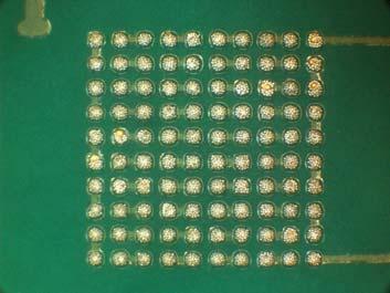
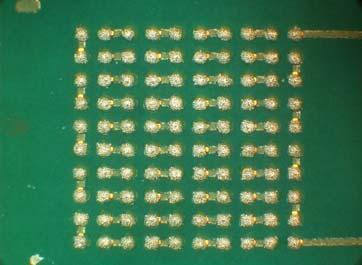
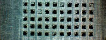
2 Test Design The stencil analysis included: 6 different stencil suppliers 9 different foil materials 5 different manufacturing processes 7 different nanocoatings The experimental design was not a full factorial. Each supplier provided stencils using technologies that were either their top performers (High End), developmental technologies that they wanted to learn more about (Supplier choices #1 and #2), or lower cost stencils commonly ordered (AR>0.70). One to four stencils were submitted by each supplier. A total of 18 stencils were print tested. All were created using the same Gerber file, and all were specified at thick with identical apertures depending on the feature. The stencil test matrix is shown in Table 1. Table 1. Test Stencil Submissions Supplier Type Letter Stencil No. 1 Supplier choice #1 2 High End A 3 AR> Supplier choice #2 5 AR> Supplier choice #2 B 7 Supplier choice #1 8 High End 9 Supplier choice #2 C 12 Supplier choice #1 13 High End D 16 AR>0.70 E 17 AR>0.70 F 18 High End AR>0.70 Supplier choice # High End Supplier choice #2 The Benchmark test vehicles were printed at the Benchmark Electronic Inc., Nashua, NH facility on a DEK 265 screen printer utilizing 18 stencils over a duration of 3 days. The solder paste was Pb-free, SAC305 no clean, Type 4 mesh. For each stencil, a total of six boards with a 10 minute delay between prints were printed by the same operator, using identical and common machine print parameters. The cards were printed in the same order and the underside of stencil was dry wiped after each print. All boards were measured with a Koh Young Solder Paste Inspection (SPI) platform. The 1st and 6 th boards were photographed to provide a visual assessment of print repeatability; these images appear in Appendix I. Each stencil was photographed after completion of the dry wipe following the 6 th print. These images also appear in Appendix I and provide a relative comparison of paste release. Specifically, stencil apertures with the less amounts of paste indicate better release. STENCIL ASSESSMENT CRITERIA This study incorporated multiple parameters to assess stencil performance: Dimensional accuracy of the aperture opening or size accuracy Visual assessment of the print and stencil after the final print to determine the amount of paste remaining in the apertures Topography of the aperture walls Analysis of SPI data for transfer efficiency and repeatability Size Accuracy of the Apertures Miniature components require apertures that are within specification. Apertures that are too small increase the risk of insufficient solder defects due to poor paste release and apertures that are too large increase the risk of bridging and solder balls. Inconsistent apertures on or 0201 components increase the risk of tombstoning. The stencil providers were asked to include 4 small coupons outside the print area that could be removed and measured for accuracy and topography assessment. The latter is a destructive test. A stencil coupon is shown in Figure 2. Figure 2. Stencil Coupon for F18. The coupon has 11 rows with various aperture openings in terms of size and shape, representing various components. Each row has 10 identical apertures to provide an indication of repeatability. The first row is a circular aperture with a specified diameter of 7.3 mils and the 2 nd row is a square aperture with a specified length and width of 7.3 mils. These two rows are nearest the typical aperture for a component. The top side and bottom sides of coupon were measured at Vicor, using a Keyence digital microscope. The location of the aperture relative to the fiducial, or location accuracy, was not measured in this study. Each measurement was ranked as target condition (green), acceptable (yellow), or unacceptable (red). A green aperture measured within +/-.3 mils to the specification, a Proceedings of SMTA International, Sep , 2016, Rosemont, IL, USA Page 623


 print to have perspective on the amount of paste remaining in the apertures.")

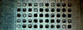
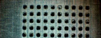
3 yellow was within +/-.3 to.5 mils, and red was outside of +/-.5 mils. The number of green, yellow and red ratings for each stencil was tabulated and the stencils ranked based on this criteria. The most accurate stencils did not have red ratings, and were ranked based on the highest number of green and fewest number of yellow ratings. The stencils with red ratings were ranked in descending order based on the number of red ratings. If two stencils had the same amount of red ratings, the number of green and yellow ratings was used to delineate the ranking. The summary appears in Table 2. Table 2. Stencils Ranking by Aperture size Accuracy Stencil Number of Green Ratings (+/-.3 mils) Number of Yellow Ratings (+/-.3 to.5 mils) Number of Red Ratings (+/-.5 to.9 mils Rank B D C D B C E C C A B B A A D A F D Visual Assessment of Print and Stencil The visual assessments of paste deposits after the first and sixth print were performed at two selected fine pitch component pads 0.3mm microbga and 0.4mm microbga locations. Each stencil was also inspected after the final (sixth) print to have perspective on the amount of paste remaining in the apertures. The photos of uncleaned stencil apertures/windows at the same two component locations were also recorded after last or 6th print. Based solely on visual inspection, the stencils were grouped into the three categories shown in Table 3. Table 3. Visual assessment of stencil apertures after 6 th print. Representative photos are shown in Appendix I. Supplier A B C D E F Ranking Above Average A1 B5 # B6 B8 C11 * D16 # D14 Average A2 A4 B7 C9 # C10 D15 E17 Below Average A3 C12 D13 F18 * Stencil was noticed stained\rusted after final print and clean (photos in Appendix I) # Relatively clean stencil having small residual film after 6 th print. The photos of typical square shape apertures both regular and with radiuses corners are shown in Figure 3. Figure 3. Square apertures with radiused corners The laser uses more energy to plunge into the middle of the aperture and less energy to provide a clean cut around the perimeter shown in Figure 4 from previous studies 1-3. Figure 4. Typical cutting path of a laser beam Topography of Aperture of Aperture Walls The roughness measurement was performed on the aperture walls of a test coupon for each stencil. The coupons were cut in half where indicated in Figures 5a and 5b, and four apertures were measured for each coupon. The topography comparison of A1 and C11 single aperture show a dramatic difference in roughness. Proceedings of SMTA International, Sep , 2016, Rosemont, IL, USA Page 624


 Bottom Inspection C9 0.69 OK E17 0.73 light bottom slag/streak B5 0.75 Ok D14 0.")

 Data Transfer efficiency (TE) and Coefficient of Variation (CV %) are excellent indicative metrics in assessment of overall")

4 Stencil A1 Streaks Figure 6b. Bottom side streaks on stencil C11 Figure 5a. Aperture Topography of Coupon A1 Stencil C11 Figure 5b. Aperture Topography of Coupon C11 Additionally, stencil C11 showed significant bottom side slag shown in Figures 6a and b, measuring over 30 microns high. This would raise the stencil off the board surface and likely would lead to excessive paste deposit volume caused by poor gasketing and allowing paste to squeeze out. Several other stencils exhibited light slag, referred to as streaks, which is believd to be related to the relative movement of the laser and table during cutting. The average roughness and bottom slag observation for all are listed in Table 4. C11 bottom Slag Table 4. Stencil Coupon Roughness and Observations Coupon # Roughness Sa (mic) Bottom Inspection C OK E light bottom slag/streak B Ok D light bottom slag/streak B sanding swirls on bottom A1 0.8 Ok B Ok D Ok A3 0.9 light bottom side streaks A Ok B Ok D light bottom side streaks D light bottom side streaks A Ok C light bottom side slag F Ok C Ok C a lot of slag The small streaks of metal measured less than 5 microns high, and would not be expected to have a major impact on volume. Analysis of Solder Paste Inspection (SPI) Data Transfer efficiency (TE) and Coefficient of Variation (CV %) are excellent indicative metrics in assessment of overall stencil print performance. In the present study these calculations were performed using inline SPI, mainly at miniature component sizes of interest: 0.3mm BGA, 0.4mm BGA and 0201H locations on all six cards printed by each stencil. The average print volume and standard deviation calculations of SPI data from six prints on each device type provide statistical indices for the comparison of each stencil s release characteristics, such as paste deposit and print repeatability. Figure 6a. Bottom side slag on C11 Proceedings of SMTA International, Sep , 2016, Rosemont, IL, USA Page 625

5 The aperture size at, 0.4mm BGA and 0201H locations were measured directly on each stencil. The theoretical volume for each aperture was calculated. The specification defined area ratios for 0.3mm BGA-square, 0.4mm BGA-square and 0201s circular shape features for 4 mil stencil thickness are 0.45, 0.55 and 0.70, respectively. The actual area ratios for these features not calculated in present work are slightly different on many stencils due to measured variation in actually cut aperture sizes. A similar study showed aperture size variation was generally within 2% on any given stencil, but as much as 22% different from stencil to stencil, which can have a considerable impact on the SMT process. 3 Transfer efficiency (TE) is calculated as the ratio of average deposit volume to the aperture volume to obtain a measure of stencil s print transferability. The Coefficient of Variation (CV %) is calculated as the ratio of standard deviation of paste volume to average paste volume and it serves as a measure of paste deposit repeatability from print to print. A generally accepted benchmark for acceptable paste transfer is 80% TE, with CV of 10% or less. Both TE and CV were determined and plotted for devices 0.3mm BGA, 0.4mm BGA and 0201s in Figures 7a and 7b. 80% 40% 0% Stencil Transfer Efficiency A1 A2 A3 A4 B5 B6 B7 B8 C10 C11 C12 C9 D13 Stencil Figure 7a. Stencil Transfer Efficiency 0.3mm BGA 0.4mm BGA 0201 Pads D14 D15 D16 E17 F Coefficient of Variation (CV %) A1 A2 A3 A4 B5 B6 B7 B8 C10 C11 C12 C9 D13 D14 D15 D16 E17 F18 0.3mm BGA 0.4mm BGA 0201 Pads Stencil Figure 7b. Assessment of Stencil Print Repeatability RESULTS AND DISCUSSION For miniaturized components, many different stencil construction technologies were tested. A wide array of results were observed. The data indicates that the best performing stencils for the miniature components appear to be B5 and B6, and D14 and D16. Interestingly, B5 and D16 had no nanocoating on them. They were cut from name brand stainless steel on new, state-of-the-art cutters. B6 and D14 were also cut on new, state-of-the-art cutters and nanocoated with thermally cured fluoropolymer nanocoating. The electroformed stencil demonstrated the poorest size accuracy of the 18 stencils tested, which is in agreement with 3 previous studies since Stencils that were laser cut with nickel overplate did not appear to perform as well as laser cut SS without overplate, with or without nanocoating. New, investigative technologies that were tested show much promise for delivering quality prints at better price points, thereby representing better values to SMT assemblers. CONTINUING WORK One of the top performing stencils is currently the process of record on Vicor s high volume production line. Because a large amount of production data already exists for this stencil configuration, a new one will not be ordered to run on the line. Instead, 2 other top performers and 2 stencils employing promising new technology will also be run for a full week in high volume production. The stencil with largest amount of slag and roughness will also be selected for volume runs to determine if these parameters impact end-of-line yields. The metrics for the production runs are, first and foremost, SPI yields. Secondary metrics include TE and Cpk for process control, and end-of-line yields. Proceedings of SMTA International, Sep , 2016, Rosemont, IL, USA Page 626
6 Prior to the stencils entering production, they will be validated using SPI to measure 2 prints each on back and front strokes, and greater than 90% yield in the first hour of production. If print yields drop below 90% and the stencil is suspected as the root cause, it will be removed from the production line and replaced with the stencil used in the process of record to investigate the suspicion. Results from the longer term production study will be published at a later date. ACKNOWLEDGEMENTS The authors would like to sincerely acknowledge and thank: Nathan Taylor and Rey Molina of Benchmark Electronics, NH for their technical support in execution of print tests and SPI programming. Stan Camin of Vicor, MA for the measurements of stencil coupons. Stencil providers for stencils and related technical support. REFERENCES [1] Whittier, R. and Shea, C., Evaluation of Stencil Materials, Suppliers and Coatings, Proceedings of SMTA International Conference, September [2] Whittier, R. and Shea, C., Fine Tuning The Stencil, Manufacturing Process and Other Stencil Printing Experiments Proceedings of SMTA International Conference, September [3] Farrell, R. and Shea, C., Stencil and Solder Paste Inspection Evaluation for Miniaturized Components Proceedings of SMTA International Conference, September Proceedings of SMTA International, Sep , 2016, Rosemont, IL, USA Page 627


7 APPENDIX I Stencil D16 Solder paste deposit on 6th card micro BGA apertures on stencil after 6 th print Stencil F18 Solder paste deposit on 6th card MicroBGA apertures on stencil after 6 th print Proceedings of SMTA International, Sep , 2016, Rosemont, IL, USA Page 628
FINE TUNING THE STENCIL MANUFACTURING PROCESS AND OTHER STENCIL PRINTING EXPERIMENTS
 FINE TUNING THE STENCIL MANUFACTURING PROCESS AND OTHER STENCIL PRINTING EXPERIMENTS Chrys Shea Shea Engineering Services chrys@sheaengineering.com Ray Whittier Vicor Corporation VI Chip Division rwhittier@vicr.com
Quantitative Evaluation of New SMT Stencil Materials
 Quantitative Evaluation of New SMT Stencil Materials Chrys Shea Shea Engineering Services Burlington, NJ USA Quyen Chu Sundar Sethuraman Jabil San Jose, CA USA Rajoo Venkat Jeff Ando Paul Hashimoto Beam
FINE TUNING THE STENCIL MANUFACTURING PROCESS AND OTHER STENCIL PRINTING EXPERIMENTS
 FINE TUNING THE STENCIL MANUFACTURING PROCESS AND OTHER STENCIL PRINTING EXPERIMENTS ABSTRACT Previous experimentation on a highly miniaturized and densely populated SMT assembly revealed the optimum stencil
FINE TUNING THE STENCIL MANUFACTURING PROCESS AND OTHER STENCIL PRINTING EXPERIMENTS
 Originally published in the Proceedings of SMTA International, Ft. Worth, TX, October, 2013 FINE TUNING THE STENCIL MANUFACTURING PROCESS AND OTHER STENCIL PRINTING EXPERIMENTS ABSTRACT Previous experimentation
The Impact of Reduced Solder Alloy Powder Size on Solder Paste Print Performance. Presented by Karl Seelig, V.P. Technology AIM Metals & Alloys
 The Impact of Reduced Solder Alloy Powder Size on Solder Paste Print Performance Presented by Karl Seelig, V.P. Technology AIM Metals & Alloys Solder Powder Solder Powder Manufacturing and Classification
Print Performance Studies Comparing Electroform and Laser-Cut Stencils
 Print Performance Studies Comparing Electroform and Laser-Cut Stencils Rachel Miller Short William E. Coleman Ph.D. Photo Stencil Colorado Springs, CO Joseph Perault Parmi Marlborough, MA ABSTRACT There
Selecting Stencil Technologies to Optimize Print Performance
 As originally published in the IPC APEX EXPO Conference Proceedings. Selecting Stencil Technologies to Optimize Print Performance Chrys Shea Shea Engineering Services Burlington, NJ USA Abstract The SMT
Can Nano-Coatings Really Improve Stencil Performance? Tony Lentz FCT Assembly
 Can Nano-Coatings Really Improve Stencil Performance? Tony Lentz FCT Assembly tlentz@fctassembly.com Outline/Agenda Introduction Claims & questions about coatings Experiment design Results of coating performance
Can Nano-Coatings Really Improve Stencil Performance? Tony Lentz FCT Assembly
 Can Nano-Coatings Really Improve Stencil Performance? Tony Lentz FCT Assembly tlentz@fctassembly.com Outline/Agenda Introduction Claims & questions about coatings Experiment design Results of coating performance
CAN NANO-COATINGS REALLY IMPROVE STENCIL PERFORMANCE?
 CAN NANO-COATINGS REALLY IMPROVE STENCIL PERFORMANCE? Tony Lentz FCT Assembly Greeley, CO, USA tlentz@fctassembly.com ABSTRACT The trajectory of electronic design and its associated miniaturization shows
DESIGN AND PROCESS DEVELOPMENT FOR THE ASSEMBLY OF PASSIVE COMPONENTS
 DESIGN AND PROCESS DEVELOPMENT FOR THE ASSEMBLY OF 01005 PASSIVE COMPONENTS J. Li 1, S. Poranki 1, R. Gallardo 2, M. Abtew 2, R. Kinyanjui 2, Ph.D., and K. Srihari 1, Ph.D. 1 Watson Institute for Systems
Broadband Printing: The New SMT Challenge
 Broadband Printing: The New SMT Challenge Rita Mohanty & Vatsal Shah, Speedline Technologies, Franklin, MA Gary Nicholls, Ron Tripp, Cookson Electronic Assembly Materials Engineered Products, Johnson City,
PCB Supplier of the Best Quality, Lowest Price and Reliable Lead Time. Low Cost Prototype Standard Prototype & Production Stencil PCB Design
 The Best Quality PCB Supplier PCB Supplier of the Best Quality, Lowest Price Low Cost Prototype Standard Prototype & Production Stencil PCB Design Visit us: www. qualiecocircuits.co.nz OVERVIEW A thin
Originally published in the Proceedings of IPC APEX/EXPO, March Development, Testing and Implementation of SAMP-Based Stencil Nano Coatings
 Originally published in the Proceedings of IPC APEX/EXPO, March 2014 Development, Testing and Implementation of SAMP-Based Stencil Nano Coatings Chrys Shea Shea Engineering Services Burlington, NJ, USA
Development, Testing and Implementation of SAMP-Based Stencil Nano Coatings
 Development, Testing and Implementation of SAMP-Based Stencil Nano Coatings Chrys Shea Shea Engineering Services Burlington, NJ, USA Ray Whittier Vicor VI CHiP Division Andover, MA, USA Eric Hanson Aculon
Chrys Shea Shea Engineering Services. Originally presented at the IPC Conference on Soldering and Reliability, November 2013, Costa Mesa, CA
 Chrys Shea Shea Engineering Services Originally presented at the IPC Conference on Soldering and Reliability, November 2013, Costa Mesa, CA Introduction to Broadband (BB) Printing Traditional and New Approaches
Chrys Shea Shea Engineering Services
 Chrys Shea Shea Engineering Services IMAPS New England 41 st Symposium and Expo May 6, 2014 PCB Layout DFM Feedback loop Component type, size, location Stencil Design Foil thickness, steps, aperture sizes
Stencil Technology. Agenda: Laser Technology Stencil Materials Processes Post Process
 Stencil Technology Agenda: Laser Technology Stencil Materials Processes Post Process Laser s YAG LASER Conventional Laser Pulses Laser beam diameter is 2.3mil Ridges in the inside walls of the apertures
AREA ARRAY TECHNOLOGY SYMPOSIUM
 AREA ARRAY TECHNOLOGY SYMPOSIUM Using SPI to Improve Print Yields Chrys Shea Shea Engineering Services/ CGI Americas Ray Whittier Vicor Corporation VI Chip Division SHEA ENGINEERING SERVICES Agenda How
Bumping of Silicon Wafers using Enclosed Printhead
 Bumping of Silicon Wafers using Enclosed Printhead By James H. Adriance Universal Instruments Corp. SMT Laboratory By Mark A. Whitmore DEK Screen Printers Advanced Technologies Introduction The technology
Investigating the Component Assembly Process Requirements
 Investigating the 01005-Component Assembly Process Requirements Rita Mohanty, Vatsal Shah, Arun Ramasubramani, Speedline Technologies, Franklin, MA Ron Lasky, Tim Jensen, Indium Corp, Utica, NY Abstract
Stencil Technology: SMTA Carolinas Chapter & GMI 17Feb11 Bill Kunkle Manager Quality & Stencil Technology MET Associates Lumberton, NJ
 Stencil Technology: 2011 SMTA Carolinas Chapter & GMI 17Feb11 Bill Kunkle Manager Quality & Stencil Technology MET Associates Lumberton, NJ 1 Current Stencil Technology Summary Processes, Materials, Capabilities,
Performance Enhancing Nano Coatings: Changing the Rules of Stencil Design. Tony Lentz
 Performance Enhancing Nano Coatings: Changing the Rules of Stencil Design Tony Lentz tlentz@fctassembly.com Outline/Agenda Introduction Experimental Design Results of Experiment Conclusions Acknowledgements
Optimization of Stencil Apertures to Compensate for Scooping During Printing.
 Optimization of Stencil Apertures to Compensate for Scooping During Printing. Gabriel Briceno, Ph. D. Miguel Sepulveda, Qual-Pro Corporation, Gardena, California, USA. ABSTRACT This study investigates
STENCIL CONSIDERATIONS FOR MINIATURE COMPONENTS
 STENCIL CONSIDERATIONS FOR MINIATURE COMPONENTS William E. Coleman, Ph.D. Photo Stencil Colorado Springs, CO, USA ABSTRACT SMT Assembly is going through a challenging phase with the introduction of miniature
A FEASIBILITY STUDY OF CHIP COMPONENTS IN A LEAD-FREE SYSTEM
 A FEASIBILITY STUDY OF 01005 CHIP COMPONENTS IN A LEAD-FREE SYSTEM Chrys Shea Dr. Leszek Hozer Cookson Electronics Assembly Materials Jersey City, New Jersey, USA Hitoshi Kida Mutsuharu Tsunoda Cookson
Ultra Fine Pitch Printing of 0201m Components. Jens Katschke, Solutions Marketing Manager
 Ultra Fine Pitch Printing of 0201m Components Jens Katschke, Solutions Marketing Manager Agenda Challenges in miniaturization 0201m SMT Assembly Component size and appearance Component trends & cooperation
Copyright: Aculon, WINNER 2014 Circuits Assembly New Product Introduction Award
 Copyright: Aculon, Inc. @ 2014 WINNER 2014 Circuits Assembly New Product Introduction Award Agenda Overview Independent Testing & Studies - Print studies - Understencil Wipe studies - Durability Testing
Solder Paste Deposits and the Precision of Aperture Sizes
 Solder Paste Deposits and the Precision of Aperture Sizes Ahne Oosterhof Eastwood Consulting Hillsboro, OR, USA ahne@oosterhof.com Stephan Schmidt LPKF Laser & Electronics Tualatin, OR, USA sschmidt@lpkfusa.com
Improve SMT Assembly Yields Using Root Cause Analysis in Stencil Design
 Improve SMT Assembly Yields Using Root Cause Analysis in Stencil Design Greg Smith FCT Assembly, Inc. gsmith@fctassembly.com This paper and presentation was first presented at the 2017 IPC Apex Expo Technical
MEASURING TINY SOLDER DEPOSITS WITH ACCURACY AND REPEATABILITY
 MEASURING TINY SOLDER DEPOSITS WITH ACCURACY AND REPEATABILITY Brook Sandy-Smith Indium Corporation Clinton, NY, USA bsandy@indium.com Joe Perault PARMI USA Marlborough, MA, USA jperault@parmiusa.com ABSTRACT:
What s Coming Down the Tracks for Printing and Stencils?
 What s Coming Down the Tracks for Printing and Stencils? Presented by: Chrys Shea, Shea Engineering Services Expert Panelists: Tony Lentz, FCT Companies Mark Brawley, Speedprint Jeff Schake, DEK-ASMPT
HOW DOES PRINTED SOLDER PASTE VOLUME AFFECT SOLDER JOINT RELIABILITY?
 HOW DOES PRINTED SOLDER PASTE VOLUME AFFECT SOLDER JOINT RELIABILITY? ABSTRACT Printing of solder paste and stencil technology has been well studied and many papers have been presented on the topic. Very
Performance of Kapton Stencils vs Stainless Steel Stencils for Prototype Printing Volumes Processes
 Performance of Kapton Stencils vs Stainless Steel Stencils for Prototype Printing Volumes Processes Hung Hoang BEST Inc Rolling Meadows IL hhoang@solder.net Bob Wettermann BEST Inc Rolling Meadows IL bwet@solder.net
APPLICATION NOTE 6381 ORGANIC LAND GRID ARRAY (OLGA) AND ITS APPLICATIONS
 AND ITS APPLICATIONS") Keywords: OLGA, SMT, PCB design APPLICATION NOTE 6381 ORGANIC LAND GRID ARRAY (OLGA) AND ITS APPLICATIONS Abstract: This application note discusses Maxim Integrated s OLGA and provides the PCB design and
Keywords: OLGA, SMT, PCB design APPLICATION NOTE 6381 ORGANIC LAND GRID ARRAY (OLGA) AND ITS APPLICATIONS Abstract: This application note discusses Maxim Integrated s OLGA and provides the PCB design and
Improve SMT Assembly Yields Using Root Cause Analysis in Stencil Design
 Improve SMT Assembly Yields Using Root Cause Analysis in Stencil Design Greg Smith FCT Assembly, Inc. Greeley, CO Abstract Reduction of first pass defects in the SMT assembly process minimizes cost, assembly
Stencil Printing of Small Apertures
 Stencil Printing of Small Apertures William E. Coleman Ph.D. Photo Stencil, Colorado Springs, CO Abstract Many of the latest SMT assemblies for hand held devices like cell phones present a challenge to
STENCIL PRINTING TECHNIQUES FOR CHALLENGING HETEROGENEOUS ASSEMBLY APPLICATIONS
 As originally published in the SMTA Proceedings STENCIL PRINTING TECHNIQUES FOR CHALLENGING HETEROGENEOUS ASSEMBLY APPLICATIONS Mark Whitmore 1 Jeff Schake 2 ASM Assembly Systems 1 Weymouth, UK, 2 Suwanee,
inemi Statement of Work (SOW) Board Assembly TIG inemi Solder Paste Deposition Project
 Board Assembly TIG inemi Solder Paste Deposition Project") inemi Statement of Work (SOW) Board Assembly TIG inemi Solder Paste Deposition Project Version # 2.0 Date: 27 May 2008 Project Leader: Shoukai Zhang - Huawei Co-Project Leader: TC Coach: Basic Project
inemi Statement of Work (SOW) Board Assembly TIG inemi Solder Paste Deposition Project Version # 2.0 Date: 27 May 2008 Project Leader: Shoukai Zhang - Huawei Co-Project Leader: TC Coach: Basic Project
Improve SMT Assembly Yields Using Root Cause Analysis in Stencil Design
 Improve SMT Assembly Yields Using Root Cause Analysis in Stencil Design Greg Smith FCT Assembly, Inc. gsmith@fctassembly.com This paper and presentation was first presented at the 2017 IPC Apex Expo Technical
Stencil Design Considerations to Improve Drop Test Performance
 Design Considerations to Improve Drop Test Performance Jeff Schake DEK USA, inc. Rolling Meadows, IL Brian Roggeman Universal Instruments Corp. Conklin, NY Abstract Future handheld electronic products
SMT Stencil, Surface Performance Returning to Basics in the SMT Screen Printing Process to Significantly Improve the Paste Deposition Operation
 SMT Stencil, Surface Performance Returning to Basics in the SMT Screen Printing Process to Significantly Improve the Paste Deposition Operation JimVillalvazo Interlatin Guadalajara, Jalisco Abstract The
VIDEO ANALYSIS OF SOLDER PASTE RELEASE FROM STENCILS. Chrys Shea Shea Engineering Services Burlington, NJ USA
 Technical Paper VIDEO NLYSIS OF SOLDER PSTE RELESE FROM STENILS hrys Shea Shea Engineering Services urlington, NJ US Mike ixenman, D... and Wayne Raney Kyzen orporation Nashville, TN Ray Whittier Vicor
RESERVOIR PRINTING IN DEEP CAVITIES
 As originally published in the SMTA Proceedings RESERVOIR PRINTING IN DEEP CAVITIES Phani Vallabhajosyula, Ph.D., William Coleman, Ph.D., Karl Pfluke Photo Stencil Golden, CO, USA phaniv@photostencil.com
IMPROVED SMT AND BLR OF 0.35MM PITCH WAFER LEVEL PACKAGES
 As originally published in the SMTA Proceedings. IMPROVED SMT AND BLR OF 0.35MM PITCH WAFER LEVEL PACKAGES Brian Roggeman and Beth Keser Qualcomm Technologies, Inc. San Diego, CA, USA roggeman@qti.qualcomm.com
PLASMA STENCIL TREATMENTS: A STATISTICAL EVALUATION
 PLASMA STENCIL TREATMENTS: A STATISTICAL EVALUATION Matt Kelly, P.Eng. 1, William Green 2, Marie Cole 3, Ruediger Kellmann 4 IBM Corporation 1 Toronto, Canada; 2 Raleigh, NC, USA; 3 Fishkill, NY, USA;
HOW DOES SURFACE FINISH AFFECT SOLDER PASTE PERFORMANCE?
 HOW DOES SURFACE FINISH AFFECT SOLDER PASTE PERFORMANCE? Tony Lentz FCT Assembly Greeley, CO, USA tlentz@fctassembly.com ABSTRACT The surface finishes commonly used on printed circuit boards (PCBs) have
SPECIFYING STENCILS TO OPTIMIZE PRINT PERFORMANCE Upper Midwest Tech Expo June 30, Chrys Shea Shea Engineering Services
 SPECIFYING STENCILS TO OPTIMIZE PRINT PERFORMANCE Upper Midwest Tech Expo June 30, 2016 Chrys Shea Shea Engineering Services PCB Layout Drives Stencil Design PCB Layout DFM Feedback loop Component type,
UNDERSTENCIL WIPING: DOES IT BENEFIT YOUR PROCESS?
 Originally published in the Proceedings of SMTA International, Orlando, FL, October, 2012 UNDERSTENCIL WIPING: DOES IT BENEFIT YOUR PROCESS? David Lober, Mike Bixenmen, D.B.A Kyzen Nashville, TN, USA david_lober@kyzen.com;
Understanding stencil requirements for a lead-free mass imaging process
 Electronics Technical Understanding stencil requirements for a lead-free mass imaging process by Clive Ashmore, DEK Printing Machines, United Kingdom Many words have been written about the impending lead-free
Troubleshooting the Stencil Printing Process
 Troubleshooting the Stencil Printing Process Chrys Shea, Shea Engineering Services Sponsored by: Topics Prin-ng Solder paste proper4es Key elements of the process Inspec-ng Phase Shi: Interferometry Typical
SOLDER PASTE STENCIL MANUFACTURING METHODS AND THEIR IMPACT ON PRECISION AND ACCURACY
 SOLDER PASTE STENCIL MANUFACTURING METHODS AND THEIR IMPACT ON PRECISION AND ACCURACY Ahne Oosterhof Oosterhof Consulting Hillsboro, OR, USA ahne@oosterhof.com Stephan Schmidt LPKF Laser & Electronics
SOLDER PASTE STENCIL MANUFACTURING METHODS AND THEIR IMPACT ON PRECISION AND ACCURACY
 SOLDER PASTE STENCIL MANUFACTURING METHODS AND THEIR IMPACT ON PRECISION AND ACCURACY Ahne Oosterhof Oosterhof Consulting Hillsboro, OR, USA ahne@oosterhof.com Stephan Schmidt LPKF Laser & Electronics
Step Stencil Technology
 Step Stencil Technology Greg Smith gsmith@fctassembly.com Tony Lentz tlentz@fctassembly.com Outline/Agenda Introduction Step Stencils Technologies Step Stencil Design Printing Experiment Experimental Results
Process Parameters Optimization For Mass Reflow Of 0201 Components
 Process Parameters Optimization For Mass Reflow Of 0201 Components Abstract The research summarized in this paper will help to address some of the issues associated with solder paste mass reflow assembly
Printing Practices for Components. Greg Smith
 Printing Practices for 01005 Components Greg Smith gsmith@fctassembly.com Outline/Agenda Introduction 01005 Components-Size, Shape and usage Stencil Design Transfer Efficiencies Q & A Introduction 01005
Printing and Assembly Challenges for QFN Devices
 Printing and Assembly Challenges for QFN Devices Rachel Short Photo Stencil Colorado Springs Benefits and Challenges QFN (quad flatpack, no leads) and DFN (dual flatpack, no lead) are becoming more popular
Investigating the Metric 0201 Assembly Process
 As originally published in the SMTA Proceedings Investigating the Metric 0201 Assembly Process Clive Ashmore ASM Assembly Systems Weymouth, UK Abstract The advance in technology and its relentless development
FLIP CHIP LED SOLDER ASSEMBLY
 As originally published in the SMTA Proceedings FLIP CHIP LED SOLDER ASSEMBLY Gyan Dutt, Srinath Himanshu, Nicholas Herrick, Amit Patel and Ranjit Pandher, Ph.D. Alpha Assembly Solutions South Plainfield,
Unlocking The Mystery of Aperture Architecture for Fine Line Printing
 Unlocking The Mystery of Aperture Architecture for Fine Line Printing Clive Ashmore ASM Assembly Systems Weymouth, Dorset Abstract The art of screen printing solder paste for the surface mount community
Meeting Future Stencil Printing Challenges with Ultrafine Powder Solder Pastes
 Meeting Future Stencil Printing Challenges with Ultrafine Powder Solder Pastes Authored by: Ed Briggs, Indium Corporation Abstract The explosive growth of personal electronic devices, such as mobile phones,
BOARD DESIGN, SURFACE MOUNT ASSEMBLY AND BOARD LEVEL RELIABILITY ASPECTS OF FUSIONQUAD TM PACKAGES
 BOARD DESIGN, SURFACE MOUNT ASSEMBLY AND BOARD LEVEL RELIABILITY ASPECTS OF FUSIONQUAD TM PACKAGES Ahmer Syed 1, Sundar Sethuraman 2, WonJoon Kang 1, Gary Hamming 1, YeonHo Choi 1 1 Amkor Technology, Inc.
Process Development And Characterization Of The Stencil Printing Process For Small Apertures
 Process Development And Characterization Of The Stencil Printing Process For Small Apertures Dr. Daryl Santos 1 and Dr. Rita Mohanty 2 1 SUNY Binghamton, Binghamton, New York, USA 2 Speedline Technologies,
FILL THE VOID III. Tony Lentz FCT Assembly Greeley, CO, USA
 FILL THE VOID III Tony Lentz FCT Assembly Greeley, CO, USA tlentz@fctassembly.com ABSTRACT This study is part three in a series of papers on voiding in solder joints and methods for mitigation of voids.
TN016. PCB Design Guidelines for 5x5 DFN Sensors. Introduction. Package Marking
 PCB Design Guidelines for 5x5 DFN Sensors Introduction This technical note is intended to provide information about Kionix s 5 x 5 mm DFN (non wettable flank, i.e. standard) packages and guidelines for
FACTORS AFFECTING STENCIL APERTURE DESIGN FOR NEXT GENERATION ULTRA FINE PITCH PRINTING
 FACTORS AFFECTING STENCIL APERTURE DESIGN FOR NEXT GENERATION ULTRA FINE PITCH PRINTING ABSTRACT: Miniaturisation is pushing the stencil printing process. As features become smaller, solder paste transfer
Application Note 5026
 Surface Laminar Circuit (SLC) Ball Grid Array (BGA) Eutectic Surface Mount Assembly Application Note 5026 Introduction This document outlines the design and assembly guidelines for surface laminar circuitry
An Investigation into Printing Miniaturised Devices for the Automotive and Industrial Manufacturing Sectors
 As originally published in the IPC APEX EXPO Conference Proceedings. An Investigation into Printing Miniaturised Devices for the Automotive and Industrial Manufacturing Sectors Clive Ashmore Mark Whitmore
SMT Troubleshooting. Typical SMT Problems For additional process solutions, please refer to the AIM website troubleshooting guide
 SMT Troubleshooting Typical SMT Problems For additional process solutions, please refer to the AIM website troubleshooting guide Solder Balling Solder Beading Bridging Opens Voiding Tombstoning Unmelted
INFLUENCE OF PCB SURFACE FEATURES ON BGA ASSEMBLY YIELD
 As originally published in the SMTA Proceedings INFLUENCE OF PCB SURFACE FEATURES ON BGA ASSEMBLY YIELD Satyajit Walwadkar, Todd Harris, Bite Zhou, Aditya Vaidya, Juan Landeros, Alan McAllister Intel Corporation
SMT Stencil, Surface Performance Returning to Basics in the SMT Screen Printing Process to Significantly Improve the Paste Deposition Operation
 SMT Stencil, Surface Performance Returning to Basics in the SMT Screen Printing Process to Significantly Improve the Paste Deposition Operation JimVillalvazo Interlatin Guadalajara, Jalisco Abstract The
BGA/CSP Re-balling Bob Doetzer Circuit Technology Inc.
 BGA/CSP Re-balling Bob Doetzer Circuit Technology Inc. www.circuittechnology.com The trend in the electronics interconnect industry towards Area Array Packages type packages (BGA s, CSP s, CGA s etc.)
BGA (Ball Grid Array)
") BGA (Ball Grid Array) National Semiconductor Application Note 1126 November 2002 Table of Contents Introduction... 2 Package Overview... 3 PBGA (PLASTIC BGA) CONSTRUCTION... 3 TE-PBGA (THERMALLY ENHANCED
BGA (Ball Grid Array) National Semiconductor Application Note 1126 November 2002 Table of Contents Introduction... 2 Package Overview... 3 PBGA (PLASTIC BGA) CONSTRUCTION... 3 TE-PBGA (THERMALLY ENHANCED
A Technique for Improving the Yields of Fine Feature Prints
 A Technique for Improving the Yields of Fine Feature Prints Dr. Gerald Pham-Van-Diep and Frank Andres Cookson Electronics Equipment 16 Forge Park Franklin, MA 02038 Abstract A technique that enhances the
Bob Willis Process Guides
 What is a Printed Circuit Board Pad? What is a printed circuit board pad, it may sound like a dumb question but do you stop to think what it really does and how its size is defined and why? A printed circuit
Ultra-Low Voiding Halogen-Free No-Clean Lead-Free Solder Paste for Large Pads
 Ultra-Low Voiding Halogen-Free No-Clean Lead-Free Solder Paste for Large Pads Li Ma, Fen Chen, and Dr. Ning-Cheng Lee Indium Corporation Clinton, NY mma@indium.com; fchen@indium.com; nclee@indium.com Abstract
To See is to Survive!
 INSPECTION SYSTEMS for the 21 s t Century To See is to Survive! In todayõs highly competitive manufacturing environment, the ability to see and react to hidden production deficiencies, in order to guarantee
TECHNICAL SPECIFICATION 2D INSPECTION Description
 D INSPECTION Description D inspection (Di) ensures the quality of the print by monitoring the printing process Di determines when a stencil clean or paste dispense is required and if licensed, to warn
Enclosed Media Printing as an Alternative to Metal Blades
 Enclosed Media Printing as an Alternative to Metal Blades Michael L. Martel Speedline Technologies Franklin, Massachusetts, USA Abstract Fine pitch/fine feature solder paste printing in PCB assembly has
VT-35 SOLDER PASTE PRINTING DEFECT ANALYSIS AND PREVENTION. Script Writer: Joel Kimmel, IPC
 VIDEO VT-35 SOLDER PASTE PRINTING DEFECT ANALYSIS AND PREVENTION Script Writer: Joel Kimmel, IPC Below is a copy of the narration for the VT-35 videotape. The contents for this script were developed by
SMT Assembly Considerations for LGA Package
 SMT Assembly Considerations for LGA Package 1 Solder paste The screen printing quantity of solder paste is an key factor in producing high yield assemblies. Solder Paste Alloys: 63Sn/37Pb or 62Sn/36Pb/2Ag
OPTIMIZING THE PRINT PROCESS FOR MIXED TECHNOLOGY
 OPTIMIZING THE PRINT PROCESS FOR MIXED TECHNOLOGY Clive Ashmore, Mark Whitmore, and Simon Clasper Dek Printing Machines Weymouth, United Kingdom ABSTRACT Within this paper the method of optimising a print
Capabilities of Flip Chip Defects Inspection Method by Using Laser Techniques
 Capabilities of Flip Chip Defects Inspection Method by Using Laser Techniques Sheng Liu and I. Charles Ume* School of Mechanical Engineering Georgia Institute of Technology Atlanta, Georgia 3332 (44) 894-7411(P)
NPL Report MATC(A)18 The Effect of Solder Alloy, Metal Particle Size and Substrate Resist on Fine Pitch Stencil Printing Performance
18 The Effect of Solder Alloy, Metal Particle Size and Substrate Resist on Fine Pitch Stencil Printing Performance") NPL Report The Effect of Solder Alloy, Metal Particle Size and Substrate Resist on Fine Pitch Stencil Printing Performance Ling Zou, Milos Dusek, Martin Wickham & Christopher Hunt August 01 NPL Report
NPL Report The Effect of Solder Alloy, Metal Particle Size and Substrate Resist on Fine Pitch Stencil Printing Performance Ling Zou, Milos Dusek, Martin Wickham & Christopher Hunt August 01 NPL Report
How Stencil Manufacturing Methods Impact Precision and Accuracy
 How Stencil Manufacturing Methods Impact Precision and Accuracy Ahne Oosterhof & Shane Stafford May 22, 2012 1. Happy Tuesday everyone, and welcome to today s webinar, How Stencil Manufacturing Methods
Contact Material Division Business Unit Assembly Materials
 Contact Material Division Business Unit Assembly Materials MICROBOND SOP 91121 P SAC305-89 M3 C Seite 1 Print Performance Soldering Performance General Information MICROBOND SOP 91121 P SAC305-89 M3 Technical
So You Want to Print to and Below.6 AAR? Jim Price Western Regional Sales Manager
 So You Want to Print to and Below.6 AAR? Jim Price Western Regional Sales Manager What is the Goal? Print to.6 and lower area aperture ratios (AAR) without the need to use exotic stencils or restricted
QUALITY SEMICONDUCTOR, INC.
 Q QUALITY SEMICONDUCTOR, INC. AN-20 Board Assembly Techniques for 0.4mm Pin Pitch Surface Mount Packages Application Note AN-20 The need for higher performance systems continues to push both silicon and
AN INVESTIGATION INTO THE DURABILITY OF STENCIL COATING TECHNOLOGIES
 AN INVESTIGATION INTO THE DURABILITY OF STENCIL COATING TECHNOLOGIES Greg Smith and Tony Lentz FCT Assembly Greeley, CO, USA This paper and presentation was first presented at the 2017 IPC Apex Expo Technical
alpha Stencils Ultra-high precision stencils for semi conductor manufacturing ALPHA Flux WLCSP Flux deposition stencils
 alpha Stencils Alpha Ultra-high precision stencils for semi conductor manufacturing ALPHA Flux WLCSP Flux deposition stencils ALPHA Sphere WLCSP Ball placement stencils ALPHA Bump bumping solder paste
COMPATIBILITY OF CLEANING AGENTS WITH NANO-COATED STENCILS
 COMPATIBILITY OF CLEANING AGENTS WITH NANO-COATED STENCILS David Lober and Mike Bixenman, D.B.A. Kyzen Corporation Nashville, TN, USA david_lober@kyzen.com and mikeb@kyzen.com ABSTRACT High density and
Journal of SMT Volume 16 Issue 1, 2003
 REAL TIME VISUALIZATION AND PREDICTION OF SOLDER PASTE FLOW IN THE CIRCUIT BOARD PRINT OPERATION Dr. Gerald Pham-Van-Diep, Srinivasa Aravamudhan, and Frank Andres Cookson Electronics, Equipment Group Franklin,
Fill the Void IV: Elimination of Inter-Via Voiding
 Fill the Void IV: Elimination of Inter-Via Voiding Tony Lentz FCT Assembly Greeley, CO, USA Greg Smith BlueRing Stencils Lumberton, NJ, USA ABSTRACT Voids are a plague to our electronics and must be eliminated!
Establishing a Precision Stencil Printing Process for Miniaturized Electronics Assembly
 Establishing a Precision Stencil Printing Process for Miniaturized Electronics Assembly Chris Anglin Indium Corporation Clinton, New York Abstract The advent of miniaturized electronics for mobile phones
USING SIGNATURE IDENTIFICATION FOR RAPID AND EFFECTIVE X-RAY INSPECTION OF BALL GRID ARRAYS
 USING SIGNATURE IDENTIFICATION FOR RAPID AND EFFECTIVE X-RAY INSPECTION OF BALL GRID ARRAYS Gil Zweig Glenbrook Technologies, Inc. Randolph, New Jersey USA gzweig@glenbrooktech.com ABSTRACT Although X-ray
B. Flip-Chip Technology
 B. Flip-Chip Technology B1. Level 1. Introduction to Flip-Chip techniques B1.1 Why flip-chip? In the development of packaging of electronics the aim is to lower cost, increase the packaging density, improve
M series. Product information. Koki no-clean LEAD FREE solder paste. Contents. Lead free SOLUTIONS you can TRUST.
 www.ko-ki.co.jp Ver. 42017e.2 Prepared on Oct. 26, 2007 Koki no-clean LEAD FREE solder paste Anti-Pillow Defect Product information This Product Information contains product performance assessed strictly
Process Control & Inspection, Assembly Programming, Reverse Engineering & Design. Products for the Electronics Industry
 Process Control & Inspection, Assembly Programming, Reverse Engineering & Design Products for the Electronics Industry COMPANY OVERVIEW Introduction Product Philosophy Agenda TECHNOLOGY AND HARDWARE PLATFORMS
BGA inspection and rework with HR 600/2 Failure analysis and assembly repair
 Even today some assemblies including BGA components still show soldering failures that require as a consequence to rework the BGA. The following example can be seen as a typical case for today s inspection
Profiled Squeegee Blade: Rewrites the Rules for Angle of Attack
 Profiled Squeegee Blade: Rewrites the Rules for Angle of Attack Ricky Bennett, Rich Lieske Lu-Con Technologies Flemington, New Jersey Corey Beech RiverBend Electronics Rushford, Minnesota Abstract For