Potential Induced Degradation (PID) of Pre-Stressed Photovoltaic Modules: Effect of Glass Surface Conductivity Disruption. Sai Ravi Vasista Tatapudi
|
|
|
- Beverly Bennett
- 5 years ago
- Views:
Transcription
1 Potential Induced Degradation (PID) of Pre-Stressed Photovoltaic Modules: Effect of Glass Surface Conductivity Disruption by Sai Ravi Vasista Tatapudi A Thesis Presented in Partial Fulfillment of the Requirements for the Degree Master of Science in Technology Approved November 2012 by the Graduate Supervisory Committee: Govindasamy Tamizhmani, Chair Devarajan Srinivasan, Member Bradley Rogers, Member ARIZONA STATE UNIVERSITY December 2012
2 ABSTRACT Potential induced degradation (PID) due to high system voltages is one of the major degradation mechanisms in photovoltaic (PV) modules, adversely affecting their performance due to the combined effects of the following factors: system voltage, superstrate/glass surface conductivity, encapsulant conductivity, silicon nitride anti-reflection coating property and interface property (glass/encapsulant; encapsulant/cell; encapsulant/backsheet). Previous studies carried out at ASU's Photovoltaic Reliability Laboratory (ASU-PRL) showed that only negative voltage bias (positive grounded systems) adversely affects the performance of commonly available crystalline silicon modules. In previous studies, the surface conductivity of the glass surface was obtained using either conductive carbon layer extending from the glass surface to the frame or humidity inside an environmental chamber. This thesis investigates the influence of glass surface conductivity disruption on PV modules. In this study, conductive carbon was applied only on the module s glass surface without extending to the frame and the surface conductivity was disrupted (no carbon layer) at 2cm distance from the periphery of frame inner edges. This study was carried out under dry heat at two different temperatures (60 C and 85 C) and three different negative bias voltages (-300V, -400V, and -600V). To replicate closeness to the field conditions, half of the selected modules were pre-stressed under damp heat for 1000 hours (DH 1000) and the remaining half under 200 hours of thermal cycling (TC 200). When the surface continuity was disrupted by maintaining a 2 cm gap i
3 from the frame to the edge of the conductive layer, as demonstrated in this study, the degradation was found to be absent or negligibly small even after 35 hours of negative bias at elevated temperatures. This preliminary study appears to indicate that the modules could become immune to PID losses if the continuity of the glass surface conductivity is disrupted at the inside boundary of the frame. The surface conductivity of the glass, due to water layer formation in a humid condition, close to the frame could be disrupted just by applying a water repelling (hydrophobic) but high transmittance surface coating (such as Teflon) or modifying the frame/glass edges with water repellent properties. ii
4 ACKNOWLEDGMENTS I would like to thank Dr. Govindasamy TamizhMani for encouraging me to work on this topic and guiding me through it. I would like to thank Dr. Bradley Rogers and Dr. Devarajan Srinivasan for being my part of my advising committee. I would also like to thank Dr. Joseph Kuitche, lab manager of ASU- PRL for his support throughout the project. I would like to thank Mrs. Sandhya Goranti and Mr. Faraz Ebneali for helping me with the initial experimental setup. I would also like to thank the following current and former ASU-PRL students for their help: Mr. Kartheek Koka, Mr. Jose Cano, Ms. Meenagupta Vemula, Ms. Quratul Ain Shah, Mr. Kolapo Olakonu, Mr. Surayanarayana Vasanthajanakiraman, Mr. Brett Knisely and Mr. Saurabh Chatterjee. Finally, I would like to thank my parents, my sister and brother-in-law for their continued support. iii
5 TABLE OF CONTENTS Page LIST OF TABLES... vi LIST OF FIGURES... ix CHAPTER 1. INTRODUCTION Background Statement of purpose Scope LITERATURE REVIEW Reliability and acceleration testing Types of Acceleration Tests Types of Conductivity Potential Induced Degradation (PID) METHODOLOGY Characterization Visual Inspection Electro-luminescence (EL) Image Inspection Performance Comparison PID Stress Equipment/Material Used Procedure RESULTS AND DISCUSSION Partial Carbon iv
6 CHAPTER Page 4.2 Full Carbon Determination of Activation Energy Charge Transferred Potential Induced Recovery Calculation of Series Resistance (R S ) Image Characterization Summary of PID Evaluations at ASU-PRL DISCUSSION REFERENCES APPENDIX A B C D E F G v
7 LIST OF TABLES Table Page 2.1. Relation between failure mechanism, field failure symptom and acceleration test Table describing the project parameters Performance comparison after PID under partial carbon condition at 60 C Performance comparison after PID under partial carbon condition at 85 C Performance comparison after PID under full carbon condition at 60 C Performance comparison after PID under full carbon condition at 85 C Activation energies of modules stressed at -300 V and 85 C Coulombs transferred Test parameters during recovery for Mfg7 under full carbon condition Power recovered after recovery test for manufacturer Series resistance values for MFG 7 modules Electro-luminescence images of a TC1 module (mfg5) Infrared images of a DH1 module (mfg6) A 1. Performance measurement of manufacturer 5 during PID testing A 2. Performance measurement of manufacturer 6 during PID testing under partial carbon condition vi
8 Table Page A 3. Performance measurement of manufacturer 7 during 35 Hrs. of partial carbon PID testing A 4. Performance measurement of manufacturer 7 during 35 Hrs. of full carbon PID testing B 1. Comparison of performance of Mfg 5 modules before and after recovery B 2. Comparison of performance of Mfg 6 modules before and after recovery B 3. Comparison of performance of Mfg 7 modules before and after recovery F 1. EL images of the MFG5 DH1 module through various test stages F 2. EL images of the MFG5 TC1 module through various test stages F 3. EL images of the MFG5 DH2 module through various test stages F 4. EL images of the MFG5 TC2 module through various test stages F 5. EL images of the MFG6 DH1 module through various test stages F 6. EL images of the MFG6 TC1 module through various test stages F 7. EL images of the MFG6 DH2 module through various test stages F 8. EL images of the MFG6 TC2 module through various test stages F 9. EL images of the MFG7 DH1 module through various test stages F 10. EL images of the MFG7 TC1 module through various test stages F 11. EL images of the MFG7 DH2 module through various test stages F 12. EL images of the MFG7 TC2 module through various test stages G 1. IR images of MFG5 DH1 module through various test stages G 2. IR images of MFG5 TC1 module through various test stages vii
9 Table Page G 3. IR images of MFG5 DH2 module through various test stages G 4. IR images of MFG5 TC2 module through various test stages G 5. IR images of MFG6 DH1 module through various test stages G 6. IR images of MFG6 TC1 module through various test stages G 7. IR images of MFG6 TC2 module through various test stages G 8. IR images of MFG6 DH2 module through various test stages G 9. IR images of MFG7 DH1 module through various test stages G 10. IR images of MFG7 TC1 module through various test stages G 11. IR images of MFG7 DH2 module through various test stages G 12. IR images of MFG7 TC2 module through various test stages viii
10 LIST OF FIGURES Figure Page 1.1. A Bath tub curve depicting failure rates at various periods in a products lifetime Voltage & polarity depending upon its position and grounding A. High Surface Conductivity (full surface carbon) B. Low Surface Conductivity C. Disrupted Surface Conductivity Equivalent circuit of a PV cell Temperature ( C) Vs. Time (h) for a thermal cycling stress test Leakage current pathways in a PV module Influence of full surface conductivity (carbon or humidity) of glass on PID at +600 V Influence of full surface conductivity (carbon or humidity) of glass on PID at -600 V String circuit diagram for an array at APS-STAR facility Influence of PID on 1,155 modules with respect to module position in the string Overall methodology followed during PID stress testing Flow chart Characterization of modules Visual inspection was performed under natural sunlight ix
11 Figure Page 3.5. An EL camera, a power supply and a computer are used to capture EL images A module is shown on an adjustable rack in front of the EL camera A module is shown to be placed securely on the rack EL images are taken before, during and after PID and recovery An example of an IR image of a module along with temperature scale The effect of light on the current-voltage characteristics of a p-n junction Daystar DS 100 IV curve tracer (top-left), Reference cells (top-right), Sundial (bottom) Performance measured using IVPC 3.05 software A keithley 2700 data logger used in the experiments Front side control panel of the PS350 power supply Circuit diagram of the PID box Modules hanging from ceramic insulators on a rack Positive from the power supply is connected to the grounding point Frame without carbon coating; Glass with carbon coating; Performance comparison after PID under partial carbon condition at 60 C for 70 hours Performance comparison after PID under partial carbon condition at 85 C Frame with carbon coating; glass with carbon Performance comparison after PID under full carbon condition at 60 C Performance comparison after PID under full carbon condition at 85 C x
12 Figure Page 4.7. Performance degradation due to PID for all the modules Influence of continuity of glass surface conductivity on PID Arrhenius plot for Mfg 5 during first 5 hours of PID stress Performance comparison before and after potential induced recovery Calculating R S of TC1 MFG7 module after full carbon PID by single slope method Calculating RS of TC1 MFG7 module after PIR by single slope method PV modules with no surface conductive layers Surface conductivity of glass with full surface carbon (A), with humidity (B), with no water layer near the frame (C) and with no carbon layer near the frame (D) V: Influence of module history, stress temperature or surface conductivity C 1. Leakage current (µa) versus time (Hrs.) for TC1 and DH1 (Mfg7) C 2. Leakage current (µa) versus time (Hrs.) for TC2 and DH2 (Mfg7) D 1. Arrhenius plot for TC1 and DH1 (Mfg 5) during first stage (5 hours of PID) D 2. Arrhenius plot for TC1 and DH1 (Mfg 5) during second stage (5 hours of PID) D 3. Arrhenius plot for TC1 and DH1 (Mfg 5) during third stage (25 hours of PID) xi
13 Figure Page E 1. Pre and post-recovery dark IVs (log scale) comparison for MFG7 DH1 module E 2. Pre and post-recovery dark IVs (log scale) comparison for MFG5 DH2 module E 3. Pre and post-recovery dark IVs (log scale) comparison for MFG7 TC1 module E 4. Pre and post-recovery dark IVs (log scale) comparison for MFG7 TC2 module xii
14 CHAPTER 1 INTRODUCTION 1.1 Background As large scale deployment of photovoltaic (PV) modules is becoming a reality, the modules must withstand various field conditions to remain operative through their warranty periods. Increased array life and reliability directly influence the economic viability of PV as an energy source. After considering present-value discounting and escalation of the worth of electricity in future, a PV plant with a 30-year life expectancy is worth % more than a plant with 20- year life expectancy [1]. Therefore, reliability of the modules plays a key role in the future adoption of PV along with the economics of both the manufacturer and the customer. The reliability trend of a product can be depicted as a bathtub curve shown in Figure 1.1. The bath tub curve shows the product failure rates in three periods. The first one, infant mortality shows the failure rates when a product is launched. This can be reduced by qualification testing to identify the possible design flaws that might occur in the first few years in the field. The second period depicts the useful life, when defects are already identified and corrected. Failures occur randomly due to manufacturing quality control issues and the overall trend is at a constant rate. The failure rates are low in this period. The third period is the endof-life period and the failure rate increases due to wear out failures. 1
15 Figure 1.1: A Bath tub curve depicting failure rates at various periods in a products lifetime. [2] The most fundamental element defining the degradation and reliability requirements is the level of applied stress. It has been reported that the following stresses play key roles in module degradation and reliability [1]. Operating temperature Humidity UV exposure Operating voltage The operating temperature has significant influence on hot-spots, encapsulant degradation, delamination, interconnect failure, etc. [1]. Most of the chemical reactions involved in degradations are a function of temperature [3]. 2
16 The presence of humidity promotes corrosion, encapsulation degradation and delamination. It can also lead to large differential expansion of stresses that aggravate delamination and fatigue [1]. UV exposure could lead to enacapsulant browning, depending upon the type of encapsulant used. System voltage has implications on the grounding requirements and electrochemical corrosions. Figure 1.2: Voltage & polarity depending upon its position and grounding [4]. Figure 1.2 shows the voltage and polarity of a module depending upon its position in an array. As an example, the negative side of an array is grounded, the modules farthest from the grounding point is under a stress of +V SYS, while the module closest to the grounding point is at 0 V. When the positive side is grounded, the farthest module is under a stress of -V SYS, while the closest module is under 0 V. When the array is ungrounded (floating), the middle module is under 0 V stress, while each of the modules at the either end of the array is under +V SYS and the other is at V SYS stress. 3
17 In typical crystalline silicon modules, potential induced degradation (PID) occurs in the modules closest to the negative voltage side of an array. The high potential difference between the cells and frame causes a polarization effect leading to leakage current discharged to the ground. Over a period of time and under the influence of high voltage, temperature and humidity, the leakage current causes potential induced degradation (PID) and reduces the module performance. 1.2 Statement of purpose The basic difference between the PID evaluations carried out by ASU- PRL and other research laboratories is the history of the test modules. The other research groups have been using fresh modules for their PID evaluations whereas the research group at ASU-PRL has been using the accelerated stress tested modules to better simulate the behavior of actual field stressed modules which might be more susceptible to the PID losses. The accelerated stress tests are: damp heat test (1000 hours at 85 o C/85%RH) and thermal cycling test (200 cycles) both per IEC The previous studies carried out at ASU-PRL indicated that: The conventional crystalline silicon PV modules are not susceptible to PID losses due to positive voltage bias The conventional crystalline silicon PV modules are susceptible to PID losses due to negative bias. The PID losses are significantly greater when a carbon layer was used for the surface conductivity of the glass superstrates and are 4
18 lower when water layer from high humidity was used for the surface conductivity of the glass superstrates. In the previous PID evaluations at ASU-PRL, the glass surface conductivity was extended to the frame by using either a carbon layer or water layer. In this study, the glass surface conductivity is disrupted near the frame edges to investigate if the PID can be interrupted just by interrupting the conductivity circuit close to the frame. The objective of this thesis is to understand the performance degradation of two damp heat (DH 1000) and two thermal cycling 200 (TC 200) stressed modules under three different voltages, two different temperatures, and two different conditions of glass surface conductivity. The primary objective of this thesis is to investigate the effect of surface conductivity disruption on PID of PV modules. 1.3 Scope by: PID effect on crystalline silicon (c-si) modules can be reduced or eliminated By modifying anti-reflective (AR) coating of the cells By increasing the bulk conductivity of encapsulant By disrupting the glass surface conductivity This work addresses the effect of surface conductivity disruption on PID. Sandhya Goranti, worked on PID under high surface conductivity. This was achieved by applying a layer of conductive carbon paste on the front glass of a PV 5
19 module, with the paste touching the module frame. The results showed that modules degrade significantly under negative bias and a high surface conductivity [5]. Figure 1.3A shows an illustration of a module under high surface conductivity. Faraz Ebneali, worked on PID under low conductivity conditions. This was achieved by stressing the samples under a relative humidity of 85%. This work found that fresh samples compared to samples that were pre-stressed under damp heat (DH) for 1000 hours would degrade significantly greater than samples that were subjected to a thermal cycling (TC) pre-stress [6]. This research also concluded, that degradation in negative bias depends on history (fresh, TC or DH) and surface conductivity [6]. Figure 1.3B shows a pictorial representation of a module under low conductivity condition. The work of this thesis will disrupt the surface conductivity of PV modules and study its effect on PID. The surface conductivity is simulated by applying a layer carbon paste. The surface conductivity is disrupted by maintaining a 2 cm gap from the edges. Figure 1.3C shows a pictorial representation of a module, when its surface conductivity is disrupted. 6

![(full surface carbon) [5] 3B:](/docs-images/89/98397075/images/20-1.jpg "Low Surface Conductivity")
![(humidity) [6] 3C: Disrupted](/docs-images/89/98397075/images/20-2.jpg "Surface Conductivity (simulated")
20 Figure 1.3A: High Surface Conductivity (full surface carbon) [5] Figure 1.3B: Low Surface Conductivity (humidity) [6] Figure 1.3C: Disrupted Surface Conductivity (simulated with partial carbon). 7
21 The scope of the current work includes the following: 1. Obtaining light current-voltage (I-V) curves of pre-stressed modules (damp heat [DH] 1000 hours; Thermal cycling [TC] 200 cycles). 2. Collecting dark I-V curves, electroluminescence (EL) and infrared (IR) images before the initiation of PID tests. 3. Performing PID on 3 projects each consisting of two DH 1000 modules and two TC 200 modules under varying: a. Voltages (-300V, -400V and -600V) b. Temperatures (60 o C and 85 o C) c. Conductivity (full and partial surface conductivity of glass superstrate using conductive carbon paste) 4. Repeating steps 1 and 2 as the final measurements to determine the PID test induced defects and performance losses. 8
22 CHAPTER 2 LITERATURE REVIEW Photovoltaics is the method of converting electromagnetic (EM) energy into electrical energy utilizing the photovoltaic effect. A solar cell is a semiconductor device, which contains an electron rich (N-type) layer(s) and a hole rich (P-type) layer(s) separated by a junction. The incoming photons energize the electrons, which move away from the junction and are collected by an external circuit [7]. According to Stephen Fonash [8], the basic four steps needed for photovoltaic energy conversion are: a) A light absorption process which causes a transition in a material (the absorber) from a ground state to an excited state, b) Conversion of the excited state into (at least) a free negative and a free positive-charge carrier pair, and c) A discriminating transport mechanism, which causes the resulting free negative-charge carriers to move in one direction (cathode) and the resulting free positive charge carriers to move in another direction (anode). d) Combining with an arriving positive-charge carrier, thereby returning the absorber to the ground state. Figure 2.1 depicts an equivalent circuit for a PV cell with the load (I L ), diode (I D ) currents and the series (R S ) & parallel (R P ) resistances. 9
23 Figure 2.1: Equivalent circuit of a PV cell [7]. 2.1 Reliability and acceleration testing Reliability of an item is defined as the ability to operate under certain conditions for a certain period of time. Reliability can be mathematically expressed as ( ) ( ) Where R (t)-reliability t- Time period, f (x)- Failure probability density function Reliability studies help to understand failure rates, causes of failure, and the anticipated lifetime of a product, so that the manufacturer has a basic understanding of their product. Lifetime prediction and causes of failure through field tests require long periods of testing which is considered a luxury in today s 10
24 competitive market. To overcome this, increasing stress levels beyond the design limits or accelerated testing may be employed. This results in the acceleration of failures with the single purpose of quantifying of the life characteristics of the product at normal use [9]. Accelerated life testing can consist of two types, qualitative accelerated life testing and quantitative accelerated life testing [10] Qualitative Accelerated Life Testing Also known as High Accelerated Life Testing (HALT), qualitative accelerated life testing reveals probable failure modes. A good qualitative test is one that quickly reveals those failure modes that will occur during the life of the product under normal use conditions [10]. HALT uses a "test-to-failure" approach employing temperature, vibration, and electrical stress exposure to rapidly precipitate and detect failures during the product development stage. Those test failures deemed relevant, or likely to cause field failures, are eliminated from the product [11] Quantitative Accelerated Life Testing These tests are designed to quantify the life characteristics of the product. Reliability information can include the determination of the probability of failure of the product under use conditions, mean life under use conditions and projected returns and warranty costs. They can also be used to assist in the performance of risk assessments, design comparisons, etc. [10]. The following table shows the required acceleration test to simulate the field failure mechanisms. 11
25 Table 2.1: Relation between failure mechanism, field failure symptom and acceleration test [12]. Failure Mechanism Field Failure Acceleration Test Moisture Penetration Delamination Damp heat Humidity freeze Moisture induced electro-chemical reaction Corrosion of cell metallization Damp heat Thermal expansion and contraction Inter-connect breakage Thermal cycling 2.2 Types of Acceleration Tests The International Electro-Technical Commission (IEC) standard (IEC second edition), identifies several environmental stress tests [13], [12]. Two of the stresses used in this study are presented below: Thermal Cycling (TC) To determine the ability of the module to withstand thermal mismatch, fatigue and other stresses caused by repeated changes of temperature. Modules are connected to a power supply (positive to positive and negative to negative) and are thermally stressed for 200 cycles. The rate of change of temperature between the low and high 12
26 extremes shall not exceed 100 C/h and the module temperature shall remain stable at each extreme for a period of at least 10 min. The cycle time shall not exceed 6 h unless the module has such a high heat capacity that a longer cycle is required [13] [12]. The number of cycles shall be as shown in the relevant blocks in the figure 2.2. Figure 2.2: Temperature ( C) Vs. Time (h) for a thermal cycling stress test [13] Damp Heat (DH) To determine the ability of the module to withstand corrosion, delamination caused by moisture penetration in high temperature-high humidity environments. The modules are introduced into a chamber at room temperature and the temperature and humidity are slowly ramped up to 85 C ±2 C and 85 % ±5 %, and are maintained under these conditions for duration of 1000 hours [13] [12]. 13
 that compose the module, e.g. Encapsulant. 2.3.2 Interface Conductivity It is the conductance through the interface between two components, e.")
27 2.3 Types of Conductivity As shown in Figure 2.4, the following three types of leakage paths could be observed in a module: Surface Conductivity Here, the leakage current travels across a conductive path established by the presence of moisture on the surface of the module Bulk Conductivity It is conductance through the bulk of the material(s) that compose the module, e.g. Encapsulant Interface Conductivity It is the conductance through the interface between two components, e.g. encapsulant/glass interface, encapsulant/cell interface and/or encapsulant/back sheet interface Figure 2.3: Leakage current pathways in a PV module [14]. The important leakage current (LC) pathways are depicted in the Figure 2.3, which shows conductance through the glass (I 1 ) and along the interfaces or 14
28 EVA contained within the module package (I 2, I 3 ) and out to the frames I 4, which shows conductance through back sheet and which was recently identified as a possible path [14]. Under a high voltage bias, one of the leakage current paths becomes predominant due to the influence of environmental factors like humidity or temperature. Under very high relative humidity, leakage currents are dominated by path I 1, i.e. conductance through the front glass, along the outer surface of glass and then to the frame. This is due to a conductance by a layer of adsorbed water on the top surface [14]. Similarly due to high relative humidity (RH), the back sheet also gets coated with water and could become conductive (I 4 ) [14]. Under a low humidity atmosphere and with a thin layer of carbon paste applied on the front surface, I 1 will be the most prominent path, while the other three paths will have negligible/ zero conductance. 2.4 Potential Induced Degradation (PID) Potential induced degradation occurs in p-type wafer based crystalline silicon modules under a negative bias [15]. This may be due to a positive charge moving towards the active area from the grounding point [16]. Positive sodium ions (Na + ) are deposited onto the active area, thus reducing the fill factor. Investigations of cell fragments on microstructural level show an accumulation of alkali metals within the SiNx anti-reflective layer, as well as at the interface to the Si. At the same location, changes of the p-n junction properties are observed [17]. This is believed to be associated with the decomposition of silicon nitride to hydrous silica and ammonia in the presence of high chemical activity of water 15
29 [18]. This can be reduced by increasing the resistivity of glass and encapsulant [16]. Also, by increasing the refractive index of the anti-reflective coating, PID could be mitigated [4]. Photovoltaic modules in the field maybe connected in series to reach the required high voltages. The typical maximum system voltage (V sys ) for series connection is 600V (United States) and 1000V (Europe). These high voltages may allow leakage currents between cell and frame/metallic mountings. High leakage current leads to electrochemical degradation. Environmental factors like temperature and humidity can have significant impact on leakage currents. Leakage currents may be potentially dangerous to workers and are also responsible for degradation due to electrochemical corrosion. Electrochemical reaction rate is proportional to the rate of inter electrode ionic charge transfer. Moisture present in the atmosphere plays an important role in PID. Research work [5], [6] at Arizona State University s Photovoltaic Reliability Laboratory (ASU-PRL) indicate that pre-stressed modules (DH1000 and TC200) experience practically no degradation at +600 V when the surface conductivity of glass is extended to the frame using a conductive carbon paste or ambient humidity (Figure 2.4). However, they degrade at -600 V when the surface conductivity of the glass is extended to the frame using the conductive carbon paste or ambient humidity (Figure 2.5). 16

30 Figure 2.4: Influence of full surface conductivity (carbon or humidity) of glass on PID at +600 V [6]. 17
 of glass on PID at -600 V (since the surface conductivity of carbon is higher than water layer (due to humidity), carbon coated modules")
31 Figure 2.5: Influence of full surface conductivity (carbon or humidity) of glass on PID at -600 V (since the surface conductivity of carbon is higher than water layer (due to humidity), carbon coated modules degrade at higher rate) [6]. Concurrently, according to other research work performed by ASU-PRL for hot-dry climatic conditions of Tempe/Arizona, the actual power plant modules under positive system voltage (negative grounded) did not exhibit PID as explained below [19]. A total of 1155 modules were connected in 55 strings of 21 modules each. Figure 2.6 shows a string circuit diagram for a typical array at the aforementioned site. Considering, the negative end of each string was centrally grounded, making the string positively biased. Module 1 is under lowest level of potential, while module 21 has the highest level of potential impressed across it 18
![[19]. Figure 2.6: String circuit diagram for an array at APS-STAR facility [19]. Figure 2.7 plots degradation percentage of all 1155 modules with respect to their position in the string, with each data point corresponding to 55 modules.](/docs-images/89/98397075/images/32-0.jpg "The total number of strings exhibiting an increasing slope, decreasing slope and constant slope of power degradation with respect to position in a string were 18, 24 and 13 respectively.")
32 [19]. Figure 2.6: String circuit diagram for an array at APS-STAR facility [19]. Figure 2.7 plots degradation percentage of all 1155 modules with respect to their position in the string, with each data point corresponding to 55 modules. The total number of strings exhibiting an increasing slope, decreasing slope and constant slope of power degradation with respect to position in a string were 18, 24 and 13 respectively. Thus, no real trend on an average was observed [19]. PID mechanism does not seem to be responsible for degradation + bias: Modules degrade at % per year, but the PID does not seem to be responsible for the degradation of negative grounded systems in the hot-dry climatic condition of Phoenix, Arizona. 19
33 Figure 2.7: Influence of PID on 1,155 modules with respect to module position in the string. Overall: No Specific Trend could be observed. 20
34 CHAPTER 3 METHODOLOGY This chapter describes the methodology applied to evaluate PID effects on PV modules. As shown in Figure 3.1, the test modules were subjected to precharacterization, PID stress and then post-characterization. Before the precharacterization tests were carried out, the test modules were pre-stressed either for thermal cycling condition (200 thermal cycles) or damp heat condition (1000 hours) according to IEC standard The thermal cycling or damp heat prestressing was carried out to simulate the field aged modules. Pre-PID Characterization PID Post-PID Characterization Figure 3.1: Overall methodology followed during PID stress testing. 21
35 Figure 3.2: Flow chart. 22
36 Module Characterization 3.1 Characterization As shown in Figure 3.3, four characterizations were carried on every test modules before PID, during PID and after PID. Additionally, they were carried out after potential induced recovery (PIR). Visual Inspection Electro-luminescence (EL) Image Inspection Infra-red (IR) Image Inspection Performance Comparison Figure 3.3: Characterization of modules Visual Inspection Modules were visually inspected for any physical defects according to Crystalline silicon terrestrial photovoltaic modules- Design qualification and type approval, IEC : 2005 [13]. Modules are inspected under natural sunlight for the following major defects. Broken/ cracked cells Broken superstrate or substrate Bubbles or delamination 23

37 Figure 3.4: Visual inspection was performed under natural sunlight The above figure 3.3 shows a module undergoing visual inspection under natural sunlight to identify any visual defects mentioned earlier Electro-luminescence (EL) Image Inspection Electro-luminescence (EL) relies on the same principle as a light emitting diode (LED). Current is fed into the module and radiative recombination of carriers causes light emission. As an indirect semiconductor, most of the recombination in silicon occurs via defects [20]. The emission is relatively low, but can be captured using a camera, which is sensitive to near IR radiation. The following procedure was used to take EL images at ASU-PRL. 1. Module is placed in a dark room with its superstrate facing the camera. 2. The module is connected to a power supply in a forward biased condition. 24

38 3. A constant current equaling to 1.3X the module I SC is injected into the module for a few minutes. 4. Using a coolsamba HR-830 camera manufactured by Sensovation AG, EL images are captured. 5. The image is studied in detail to identify any defects. Figure 3.5: An EL camera, a power supply and a computer are used to capture EL Figure 3.6: A module is shown on an adjustable rack in front of the EL camera. images. 25

39 Figure 3.7: A module is shown to be placed securely on the rack. Figures 3.4 and 3.5 show the EL imaging studio at ASU-PRL. It comprises of aforementioned equipment like an EL camera, a power supply and a computer along with an adjustable rack for mounting the test sample. Figure 3.6 shows a close-up of the module on its rack. Figure 3.7 shows a sample EL image, it is clearly seen that some cells in the module have turned darker or even stopped emitting. These are the problem areas, where the cells are dead. Modules are also thoroughly studied using IR and UV images to corroborate these findings. 26
 Image Inspection A typical solar module converts only 10-20 % of the incident irradiance, while the rest is either reflected, or dissipated as heat, and electromagnetic radiation.")
40 Figure 3.8: EL images are taken before, during and after PID and recovery Infra-red (IR) Image Inspection A typical solar module converts only % of the incident irradiance, while the rest is either reflected, or dissipated as heat, and electromagnetic radiation. Defects like hot-spots could be easily detected using an IR camera. The following procedure has been followed to capture IR images of the modules. 1. Module is placed on tracker/ roof-top under a natural irradiance of not less than 1000 W/m 2 [13]. 2. Leads of the module are shorted and the module is exposed to irradiance for about 5-10 minutes. 3. Using a Ti55FT IR camera, manufactured by Fluke Corporation, images are captured. Capturing the images during 11AM-2PM on a clear sunny day with a wind speed of 1m/s, would see that the images free from errors caused by environmental factors. Figure 3.8 shows an IR image for a test sample. 27


41 Figure 3.9: An example of an IR image of a module along with temperature scale Performance Comparison The IV curve of a solar module is the superposition of the IV curve in the dark with the light-generated current. Figure 3.6 shows the effect of light on the current-voltage characteristic on a p-n junction diode. The IV curve of a solar cell is the superposition of the IV curve of the solar cell diode in the dark with the light-generated current. The light has the effect of shifting the IV curve down into the fourth quadrant where power can be extracted from the diode. Illuminating a cell adds to the normal "dark" currents in the diode so that the diode law becomes [ ( ) ] I- Total current (A) I 0 - Saturation current of the diode (A) I L - Light generated current (A) V- Cell voltage (V) 28
 Figure 3.")

42 q- Elementary charge (1.6 x C) n- Ideality factor (usually 1 or 2) k- 1.38x10⁻²³J/K T- Cell temperature (K) Figure 3.10: The effect of light on the current-voltage characteristics of a p-n junction [21]. Figure 3.11: Daystar DS 100 IV curve tracer (top-left), Reference cells (top-right), Sundial (bottom). 29
43 An IV curve tracer is able to provide both a qualitative visual representation and a quantitative measure of PV performance. In brief, a curve tracer uses a capacitive load to vary the impedance connected to the output terminals of the PV module [22]. Figure 3.7 shows the curve tracer used, along with reference cells to measure the irradiance, and a sun dial (in-plane with the module) used to keep the modules normal to the radiant beam. The current-voltage characteristic of the module was measured using a DS100 IV curve tracer, manufactured by Daystar, Inc. The performance was measured under natural sunlight when the irradiance was above 900 W/m 2 and module temperature varying between 20 C and 50 C. The following procedure is followed for performance measurements. 1. Module was initially placed in an environmental chamber and cooled down to about 15 C. 2. Module was then placed on a tracker under natural sunlight, with the tracker facing normal to the radiant beam. This can be achieved with the help of a sundial. 3. The module was connected to the curve tracer and at least 10 curves are taken between 20 C and 50 C. 4. A reference cell was used to measure the irradiance. 5. Ambient air and reference cell temperatures were also duly recorded. Since photovoltaic system performance depends on irradiance and operating temperature, normalizing is used to translate IV curves taken at one set of irradiance and temperature conditions to a different set of irradiance and 30

44 temperature conditions. This is done so that IV curves taken under different coditions can be compared as if they were taken under identical conditions. Uually curves are normalized to standard conditions of irradiance at 1000 W/m2 and temperature at 25 C. ASTM E method was used to normalize the IV curves using IVPC software. The average powers after each test are then compared to determine the power loss of the module due to PID. Figure 3.8 shows a screen shot of the IVPC software, which was used to collect IV curves and normalize them. Figure 3.12: Performance measured using IVPC 3.05 software. 31

45 3.2 PID Stress The following steps describe the equipment used, and the procedure followed to induce PID stress on modules Equipment/Material Used a) Keithley 2700 data acquisition system A Keithley 2700 data logger shown in Figure 3.9 having a resolution of 0.1 µv is used to measure the leakage current in the circuit [23]. The voltage across a resistor in the PID box is measured and the leakage current is calculated using Ohm s law. I-Leakage current (A) V-Voltage across the resistor (V) R-Resistance of the resistor (Ω) Figure 3.13: A keithley 2700 data logger used in the experiments. [24] 32

46 b) PS350 high voltage power supply A power supply having a range of ± 50 V to ± 5 kv and a maximum current of 5 ma is used to induce high voltage on the samples. Figure 3.9 shows the front control panel of the Stanford Research Systems, PS350 power supply. It is capable of producing 25 Watts at a maximum voltage of 5000 V. Figure 3.14: Front side control panel of the PS350 power supply. c) PID Resistor Box Since the leakage current in the circuit is beyond the sensitivity of the datalogger, voltage across a known resistance is measure instead and the leakage current is calculated using Ohm s law. It consists of a series of resistors are in the circuit in between the module and the power supply. The 100 kω resistors act as a safety device to protect the power supply during fault situation, while voltage measured across the 5 kω resistor is used to calculate the leakage current. Figure 3.11 shows the circuit diagram of the PID resistor box. 33
![Figure 3.15: Circuit diagram of the PID box showing the modules, resistors, and the power supply [25].](/docs-images/89/98397075/images/47-0.jpg "d) Carbon paste Under damp conditions, a thin but continuous layer of moisture is formed on the front glass of the module.")
47 Figure 3.15: Circuit diagram of the PID box showing the modules, resistors, and the power supply [25]. d) Carbon paste Under damp conditions, a thin but continuous layer of moisture is formed on the front glass of the module. As mentioned in the literature review, a leakage path could be established due to this layer. To simulate this, layer, a thin layer of a conductive carbon paste is applied on the front glass of the module. The carbon paste used in the experiments is MG Chemicals 846 carbon conductive paste, having an electrical resistivity of 117 Ω.cm and conductivity of 8.57 ms.cm. 34
.")
48 Figure 3.16: Modules hanging from ceramic insulators on a rack Procedure The superstrate of the module was covered with a thin layer of conductive carbon.. The carbon layer was extended from the glass surface to the frame for certain number of modules (referred as full carbon ). For the other modules, in order to disrupt the conductivity/continuity, the carbon layer was not extended to the frame and the layer coverage was stopped 2 cm away from the edge of the frame (referred as partial carbon ). The module was then placed in an environmental chamber on a rack as shown in figure The modules are separated from the rack by ceramic insulators and teflon strips. Module leads was shorted and connected to the negative lead of the power supply, while the positive from the power supply is 35
 was applied.")
49 connected to the grounding point on the module as shown in figure Figure 3.17: Positive from the power supply is connected to the grounding point. The power supply was turned ON and the required negative voltage (see Table 3.2) was applied. Temperature inside the chamber is increased at a rate of 1 C/min The temperature and voltage were maintained for a total duration of 35 hours. In case of Mfg5 & 6, they are tested in two cycles of 5 hours, and one cycle of 25 hours. The temperature was decreased to ambient temperature at a rate of 1 C/min. Voltage is turned OFF. Module performance was measured and compared with previous performance. Table 3.1: Table describing the project parameters. 36
50 Project Group Temperature ( C) Voltage (V) Mfg V V Mfg V V Mfg V V Table 3.1, provides, the stress parameters to be used for the test samples. 37

51 CHAPTER 4 RESULTS AND DISCUSSION This chapter contains experimental results and data analysis. The catastrophic effects of carbon paste touching the frame was identified and the test procedure was modified to compare the test results obtained between the partial carbon coating condition and the full carbon coating condition. 4.1 Partial Carbon The modules were coated with a thin layer of carbon layer to increase their surface conductivity as shown in Figure 4.3. However, the paste was applied on the glass surface in such a fashion that it did not come into contact with the module frame. A space of 2 centimeters was maintained between the inner edge of the frame and the boundary of carbon coating. This coating method basically disrupted the continuity of the surface conductivity from the glass to the frame. 2 cm. 2 cm. Figure 4.1: Frame without carbon coating; Glass with carbon coating; 38
52 The modules were stressed at various voltages and temperatures with this interrupted surface conductivity. Table 4.3 and Figure 4.4 show the performance results of modules before and after PID stress test at 60 C. 39
53 Table 4.1: Performance comparison after PID under partial carbon condition at 60 C. Before partial carbon PID (W) After partial carbon PID (W) % of Power remaining Applied Voltage (V) PID Duration (hours) Manufacturer 5 TC DH Manufacturer 6 TC DH Manufacturer 7 TC DH Average It can be seen that on average, the modules lost less than 1.5 % of their initial power due to PID stress at 60 C irrespective of manufacturer (Mfg 5, 6 or 7), stress voltage (-300, -400 or -600 V) or history of accelerated stressing (DH or TC). Two modules (a DH and a TC) have shown a slight increase in their output after 70 hours of PID. One module is a mono-silicon module stressed at -600 V, while other is a poly-silicon module stressed at -400 V. The power increase, although very small (less than 0.6%), might be due to measurement repeatability error and it is within the practicing industry standard limit of 1%. 40

54 Figure 4.2: Performance comparison after PID under partial carbon condition at 60 C for 70 hours. Table 4.4 and Figure 4.5 show the performance results of the modules under partial carbon condition at 85 C. It can be seen that on average, the modules lost less than 0.20 % of their initial power due to PID stress at 85 C irrespective of manufacturer (Mfg 6 or 7), stress voltage (-400 or -600 V) or - history of accelerated stressing (DH or TC). 41
 After partial carbon PID (W) % of Power remaining Applied Voltage (V) PID Duration (hours) Manufacturer 6 TC1 194.0 198.4 102.3 DH1 205.8 199.5 96.")
55 Table 4.2: Performance comparison after PID under partial carbon condition at 85 C. Before partial carbon PID (W) After partial carbon PID (W) % of Power remaining Applied Voltage (V) PID Duration (hours) Manufacturer 6 TC DH V 35 Manufacturer 7 TC DH V 70 Average 99.8 Figure 4.3: Performance comparison after PID under partial carbon condition at 85 C. 42
 coated with carbon paste.")
56 4.2 Full Carbon In the full carbon condition, the modules were completely coated with a thin layer of carbon paste to increase their surface conductivity, unlike the partial carbon condition, where the paste did not come into contact with the module frame. The photograph shown in Figure 4.4 provides a view of a module completely (both glass and frame) coated with carbon paste. It should be noted that these modules from manufacturer 7 (mfg 7) already underwent 70 hours of PID stress under partial carbon coating condition testing and they were reused to see the effect of full carbon coating on the glass and frame. Figure 4.4: Frame with carbon coating; glass with carbon Table 4.3 and Figure 4.5 show the performance results of modules before and after PID stressing at -600 V and 60 C for 35 hours. It is seen that the TC and DH modules retain only about 67.0 % and 16.2 % of their pre-stress power. The average drop for two modules (MFG7: TC1, DH1) due to full surface conductivity at 60 C is about 58.4%, whereas, it is only less than 0.6% average 43
57 power drop due to interrupted/partial surface conductivity. In comparison, the average power drop due humidity is about 30% [6]. Table 4.3: Performance comparison after PID under full carbon condition at 60 C. Before full carbon PID (W) After full carbon PID (W) % of Power remaining Applied Voltage (V) PID Duration (hours) Manufacturer 7 TC DH hours (partial carbon coating) + 35 hours (full carbon coating) Figure 4.5: Performance comparison after PID under full carbon condition at 60 C. Table 4.4 and Figure 4.6 show the performance results of the modules stressed at 85 C under full carbon condition. All the modules are mono-silicon 44
58 modules with two from Mfg 5 stressed under -300 V and two from Mfg 7 stressed under -600 V. Table 4.4: Performance comparison after PID under full carbon condition at 85 C. Before full carbon PID (W) After full carbon PID (W) % of Power remaining Applied Voltage (V) PID Duration (hours) Manufacturer 5 TC DH Manufacturer 7 TC DH hours (partial carbon) + 35 hours (full carbon) Figure 4.6: Performance comparison after PID under full carbon condition at 85 C. 45
59 From Table 4.4 and Figure 4.8, it is shown that the modules have lost significant amount of power, with the DH modules losing more than the TC modules. This was expected and was also reported by Sandhya Goranti [5] and Faraz Ebneali [6]. The average power drop for four modules (MFG5: TC1, DH1; MFG7: TC1, DH1) due to full surface conductivity at 85 C is approximately79.4 %. In comparison, the average power drop due to humidity is approximately 22.1% [6]. The average power drop due to full surface conductivity at both temperatures (85 C and 60 C) for the six modules (MFG5: TC2, DH2; MFG7: TC1, TC2, DH1, DH2) is approximately 72.4 %. The full carbon condition has a very adverse effect on the modules and it does not appear to simulate the naturally occurring humidity condition where the surface conductivity is very limited and interfacial conductivity (glass/encapsulant; cell/encapsulant; encapsulant/backsheet) could also occur. Therefore, it is recommended to utilize the humidity based surface conductivity method rather than carbon (or any metallic layer) based surface conductivity method. Figure 4.7 shows the remaining power of all the modules tested in this thesis work. 46


60 Figure 4.7: Performance degradation due to PID for all the modules. Figure 4.8: Influence of continuity of glass surface conductivity on PID 47
61 Figure 4.8 depicts the percent of power remaining for modules that underwent PID under the partial carbon condition and then under the full carbon condition. From the above, it is evident that degradation is negligible/ nonexistent under the partial carbon condition, while it is detrimental in full carbon condition. Since, surface conductivity is the predominant conductive path [6], disrupting it drastically reduces or eliminates the PID effect. Therefore, applying a 2 cm wide layer of water repellant (e.g. Teflon) on the edges of module is expected to either prevent or drastically reduce PID from occurring. In the previous studies, the performance of the modules was found to have degraded significantly at the negative bias when the surface conductivity was existing (either through carbon layer extending to the frame or humidity). When the surface continuity in this current study was disrupted by maintaining a 2 cm gap from the frame to the edge of the conductive layer, the degradation was found to be absent or negligibly small, even after 35 hours under negative bias and at elevated temperatures. This preliminary study appears to indicate that if the continuity of the glass surface conductivity is disrupted at the inside boundary of the frame, the modules could become immune to PID losses. Previous studies by other research groups indicated that the PID losses can be contained either by modifying the anti-reflection coating of the cells or the encapsulant bulk resistivity. This preliminary study indicates the PID losses could be contained by disrupting the surface conductivity of the glass at the inside boundary of the frame. The surface conductivity of the glass due to water layer formation under humid conditions could be disrupted by the following methods; applying a water 48
62 repelling (hydrophobic) close to the frame such as a highly transmittance surface coating (such as Teflon) or modifying the frame/glass edges with water repellent properties. The finding of this preliminary study is recommended to be extended with a larger number of test samples from a larger number of manufacturers so the surface conductivity disruption effect on PID can be fully analyzed and understood. The full carbon coated results shown in Figures 4.7 and 4.8 also indicate the following: The DH stressed modules seem to undergo higher PID losses as compared the TC stressed modules, and this result is consistent with previous findings [6]. The 85 o C temperature condition for the PID evaluation seems to be very aggressive as compared to the 60 o C temperature condition. The 85 o C temperature condition with fully covered metallic conductive surface may not be simulating the actual field failure mechanism related to PID. 4.4 Determination of Activation Energy Activation energy is defined as the minimum amount of energy required to initiate a reaction. The higher the temperature, the faster the reaction will occur. While the temperature increases, the electron collision rate within the interfaces accelerates and results in a higher kinetic energy which will affect the activation energy. The rate of the PV module deterioration can potentially be predicted by using the Arrhenius equation. In general, Arrhenius plots are used to analyze the effect of temperature on the rates of chemical reactions. The Arrhenius equation 49
63 can explain the rate of reaction depending on the temperature that the sample is tested [6].The governing Arrhenius equation is- ( ) r- Rate of failure A- Proportional constant E a - Activation energy (ev) T- Absolute temperature ( K) k- Stefan-Boltzmann constant = 8.6 x 10⁻⁵ (ev/k) Using the module failure rates at high temperatures and the Arrhenius equation we can predict the reaction rates at lower temperatures by extrapolating the Arrhenius curve [5]. Figure 4.11 shows the Arrhenius plots for the first five hours of modules TC 1 and DH 1 under full carbon condition. Figure 4.9: Arrhenius plot for Mfg 5 during first 5 hours of PID stress. 50
64 Table 4.5 provides the activation energy of the modules during 5 hours, 10 hours and 35 hours at -300V stress voltage. During the first 5 hours, the modules were stressed under the full carbon condition, whereas, they were stressed under partial carbon condition for the rest of the test. This is evident in a higher activation energy during first 5 hours, than the second. Table 4.5: Activation energies of modules stressed at -300 V and 85 C. Note that, for the first 5 hours, the modules were stressed under full carbon condition. Module PID Stress Temperature ( C) After 5hr PID (Full (ev) After 10hrs PID (Partial (ev) After 35hrs PID (Partial (ev) TC DH Module PID Stress Temperature ( C) After 5hr PID (Partial (ev) After 10hrs PID (Partial (ev) After 35hrs PID (Partial (ev) TC DH Charge Transferred Due to the leakage current over the test period, a charge is transferred. The following formula gives us the charge transferred to the module. Where C- Charge transferred I- Sum of the leakage current over test period 51
65 T- Test time Table 4.6: Charge (Coulombs) transferred. 0-5hrs 5-10hrs 10-35hrs Module (full carbon) (Coulomb) (partial carbon) (Coulomb) (partial carbon) (Coulomb) TC DH hrs 5-10hrs 10-35hrs Module (partial carbon) (Coulomb) (partial carbon) (Coulomb) (partial carbon) (Coulomb) TC NA DH NA From the table 4.6 above, it can be concluded that the charge transferred is high due to the carbon paste touching the frame and increasing the conductivity multiple folds. 4.6 Potential Induced Recovery After stressing the modules for a cumulative time of 105 hours, the modules were stressed under positive (+) bias for 35 more hours to recover their lost power. The following table shows the parameters used for recovering the modules. In addition, full carbon condition was used during recovery. Table 4.7: Test parameters during recovery for Mfg7 under full carbon condition. 52
66 Manufacturer 7 Parameter Group1 Group2 Voltage +600 V +600 V Temperature 85 C 60 C Relative Humidity 0-5 % 0-5 % Time 35 Hrs. 35 Hrs. Table 4.8: Power recovered after recovery test for manufacturer 7. Manufacturer 7 Module Temperature ( C) After PID (W) % Remaining PID After (W) % Remaining TC DH TC DH Table 4.10 shows the power recovered by the modules after recovery testing. It can be seen that the modules have recovered a significant amount of power after only 35 hours of recovery. Further recovery testing may enhance the power recovered. 53
67 Figure 4.10: Performance comparison before and after potential induced recovery. 4.7 Calculation of Series Resistance (R S ) Using the single slope method, a single light I-V curve at an irradiance of 1000W/m2 was collected to determine Rs value. By selecting 30 data points close to the open circuit voltage (Voc) of an IV curve, and obtaining a linear fit to the extracted data, Rs is calculated as inverse of slope of the linear curve. 54
68 Figure 4.11: Calculating R S of TC1 MFG7 module after full carbon PID by single slope method. Figure 4.12: Calculating RS of TC1 MFG7 module after PIR by single slope method. The two plots above shows I-V curves before full carbon PID and post- PIR. The series resistance is the inverse of the slope of the curve, which for the 55
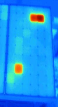
69 above value are 2.19 Ω and 1.72 Ω. The following table consists of R S values of MFG7 modules. Table 4.9: Series resistance values for MFG 7 modules. R S After PID R S After PIR TC DH TC DH Image Characterization As described in Chapter 3, a visual inspection was performed on every module, followed by electro-luminescent (EL) imaging and infra-red (IR) imaging. Table 4.12 consists of EL images of TC1 (mfg5) module before, during & after PID and after recovery. These modules were stressed in the full carbon condition for the first 5 hours of PID and then under the partial carbon condition. The module degradation is clearly visible, with no current being produced by the dark areas. From this, we can conclude that most of the degradation occurred during 5 hours of PID full carbon condition. Also, the EL images show us that the DH modules are more susceptible to PID than TC modules. 56


70 Table 4.10: Electro-luminescence images of a TC1 module (mfg5). Pre-PID Stressed 5 hrs. into PID (Full 10 hrs. into PID (Partial 35 hrs. into PID (Partial 35 hrs. into PIR (Full From the following IR images (Table 4.13) of a DH module, it is observed that the module post recovery has three extreme hot spots which are about 35 C to 40 C hotter than the rest of the module. In addition there were three other hot 57


71 spots which were about 20 C higher than their surroundings cells. This may allude to some mechanism where the module degraded during the recovery process. Table 4.11: Infrared images of a DH1 module (mfg6) Before PID After 10 Hrs. of PID (Partial After 35 Hrs. of PID (Partial After 35 Hrs. of PIR (Full 4.8 Summary of PID Evaluations at ASU-PRL section. The PID study performed so far at ASU-PRL is summarized in this PID effect of c-si modules can be reduced or eliminated by: 1) By modifying AR coating of the cells 58
72 2) By increasing the bulk conductivity of encapsulant 3) By disrupting the glass surface conductivity The influence of surface conductivity, including the conductivity disruption, of the glass on PID is presented below. Figure 4.13 shows the PV modules with no surface conductive layers. Figure 4.14 shows the PV modules with high surface conductive layer of carbon (Figure 4.14A), low surface conductive layer of water (Figure 4.14B), disrupted conductive layer of water (Figure 4.14C) and disrupted conductive layer of carbon (Figure 4.14D). Figure 4.14D simulates the disrupted conductivity of glass surface due to the absence of water layer near the frame. The absence of water layer near the frame may be achieved by using a hydrophobic layer near the frame or by treating the glass surface near the frame for hydrophobicity. The objective of this work is to investigate if the PID effect can be decreased or eliminated by disrupting the glass surface conductivity near the frame edges. 59


73 Figure 4.13: PV modules with no surface conductive layers 60

 and with no carbon layer near the frame for disrupted")
74 (A) (B) (C) (D) Figure 4.14: Surface conductivity of glass with full surface carbon for high surface conductivity (A), with humidity for low surface conductivity (B), with no water layer near the frame for disrupted conductivity (C) and with no carbon layer near the frame for disrupted conductivity (D). figure 4.14D simulates Figure 4.14C condition. 61
![Figure 4. 15: +600V: Influence of module history, stress temperature or surface conductivity [26] Figure 4.15 compares the percentage of power remaining in the modules after a +bias stress.](/docs-images/89/98397075/images/75-0.jpg "Mfg1 modules were stressed under the full carbon (high conductivity) condition, while the mfg2 and mfg3 were stressed under low surface conductivity (85% RH).")
75 Figure 4. 15: +600V: Influence of module history, stress temperature or surface conductivity [26] Figure 4.15 compares the percentage of power remaining in the modules after a +bias stress. Mfg1 modules were stressed under the full carbon (high conductivity) condition, while the mfg2 and mfg3 were stressed under low surface conductivity (85% RH). The modules under + bias had [26]: No PID effect irrespective of history of modules No PID effect irrespective of level (high or low) of surface conductivity No PID effect irrespective of manufacturer 62
![Figure 4.16: -600V: Influence of module history, stress temperature or surface conductivity [26]. Figure 4.](/docs-images/89/98397075/images/76-0.jpg "16 compares the percentage of power remaining in the modules after they underwent PID under bias.")
76 Figure 4.16: -600V: Influence of module history, stress temperature or surface conductivity [26]. Figure 4.16 compares the percentage of power remaining in the modules after they underwent PID under bias. The modules under negative bias had [5] [6]: The PID effect depending on the history of modules The PID effect depending on the level (high or low) of surface conductivity The PID effect depending on the manufacturer 63

![The test results modules under negative bias with disrupted surface conductivity seem to indicate [this thesis work]:](/docs-images/89/98397075/images/77-1.jpg "No PID effect irrespective of history of modules No PID effect irrespective of PID stress temperature No PID effect")
77 Figure 4.17: Influence of module history, PID stress temperature and glass surface conductivity. Figure 4.17 compares the percentage of power remaining in the modules after they underwent PID under negative bias. The test results modules under negative bias with disrupted surface conductivity seem to indicate [this thesis work]: No PID effect irrespective of history of modules No PID effect irrespective of PID stress temperature No PID effect irrespective of manufacturer 64
78 CHAPTER 5 CONCLUSIONS In this study, the PV modules from three different manufacturers were investigated for the potential induced degradation. The following key conclusions may be obtained: Influence of glass surface conductivity: Irrespective of history, PID stress temperature or PID stress voltage, the average drop due to full carbon surface conductivity is 73% and due to partial carbon conductivity is only less than 1%. Influence of pre-history: Irrespective of PID stress temperature or PID stress voltage, the average drop due to damp heat pre-history is about 2% and due to thermal cycling pre-history is about 0% when the surface conductivity is disrupted. Influence of PID stress temperature: Irrespective of pre-history or PID stress voltage, the average drop due to 60 C and 85 C PID stress when the surface conductivity is disrupted is zero or negligibly small. Some other conclusions that could be made from this research and previous works conducted at ASU-PRL are: Under a positive voltage bias, no degradation was observed for hot-dry climatic conditions. Under a negative voltage bias, significant degradation was observed. 65
79 Under high-surface conductivity, higher degradation was observed. Failure mechanism under negative voltage bias appears to be mostly or fully reversible by applying a positive voltage. studies. The following are a few suggestions that might be useful during future All samples should be from the same manufacturer and of same model. Due to various factors, dark IV could not be obtained until the final stages of testing. Having dark IVs would greatly helpful in the calculation of the series resistance. Further studies could be made on Optimum width of the moisture repellant/ conductivity disrupting layer. Why TC modules are developing higher resistance to PID? Increasing stress voltage to 1500 V. Increasing the stress time. Increasing number of samples. 66
80 REFERENCES [1] R. G. Ross, "Crystalline-silicon, reliability lessons for thin-film modules," in 18th IEEE Photovoltaic Specialists Conference (PVSC), Las Vegas, NV, [2] "Bath tub curve," [Online]. Available: [3] G. Mon and R. G. Ross, "Effects of temeperature and moisture on module leakage currents," in 18th IEEE Photovoltaic Specialists Conference (PVSC), Las Vegas, NV, [4] Pingel, S; Frank, O; Winkler, M; Dyran, S; Geipel, T; Hoehne, H; Berghold, J;, "Potential Induced Degradation of Solar Cells and Panels," in 35th IEEE Photovoltaic Specialists Conference (PVSC), Honolulu, HI, [5] S. Goranti, "Potential Induced Degradation (PID) of Accelerated Stressed Photovoltaic Modules," [6] F. Ebneali, "Potential Induced Degradation of PV Modules: Influence of Temperature and Surface Conductivity," [7] R. H. Bube, Photovoltaic Materials, Imperial College Press, [8] S. Fonash, Solar Cell Device Physics, Academic Press, 2010, p. 1. [9] "What is accelerated life testing?," [Online]. Available: [Accessed 18 November 2011]. [10] "Types of Accelerated Tests," [Online]. Available: [Accessed 18 November 2011]. 67
81 [11] M. L. Morelli, "Effectiveness of HALT and HASS," [Online]. Available: [12] J. H. Wohlgemuth and M. D. Frederick, "Reliability Testing of PV Modules," in Photovoltaic Energy Conversion, 1994., Waikoloa, HI, [13] International Electrotechnical Commission (IEC) standard, IEC 61215, 2.0 ed., International Electrotechnical Commission, [14] J. A. del Cueto and S. R. Rummel, "Degradation of Photovoltaic Modules Under High Voltage Stress in the Field," in Reliability of Photovoltaic Cells, Modules, Components, and Systems III: SPIE Conference, San Diego, CA, [15] P. Hacke, S. Glick, S. Johnston, R. Reedy, J. Pankow, T. Kent and S. Kurtz, "Influence of Impurities in Module Packaging on Potential-Induced Degradation," in 22nd Workshop on Crystalline Silicon Solar Cells & Modules: Materials and Processes, Vail, Colorado, [16] P. Hacke, M. Kempe, K. Terwilliger, S. Glick, N. Call, S. Johnston, S. Kurtz, I. Bennett and M. Kloos, "Characterization of Multicrystalline Silicon Modules with System Bias Voltage Applied in Damp Heat," in 25th European Photovoltaic Solar Energy Conference and Exhibition (EUPVSEC), Valencia, [17] V. Naumann, C. Hagendorf, S. Grosser, M. Werner and J. Baghdan, "Micro Structural Root Cause Analysis of Potential Induced," in 2nd International Conference on Crystalline Silicon Photovoltaics, [18] K. Morita and O. Kiyoki, "Novel Selective Etching Method for Silicon Nitride Films on Silicon Substrates by Means of Subcritical Water," Ind. Eng. Chem. Res., vol. 39, no. 12, p , 28 October [19] J. Singh, "Investigation of 1,900 individual field aged photovoltaic modules for potential induced degradation (PID) in a positive biased power plant,"
82 [20] C. Honsberg and S. Bowden, "Electroluminescence," [Online]. Available: [Accessed August 2011]. [21] C. Honsberg and S. Bowden, "IV Curve," [Online]. Available: [22] "Description," [Online]. Available: [23] "2700 Datalogger," [Online]. Available: [24] "Keithley 2700 DMM," [Online]. Available: [25] "PID Test System, Instruction Manual, ASU Photovoltaic Reliability Laboratory," [26] G. Tamizhmani, "Potential Induced Degradation: Analysis of 1900 Individual Modules," in 2012 (PVMRW), Golden, CO, [27] "Carbon Conductive Grease 846," [Online]. Available: [Accessed November 2011]. [28] International Electrotechnical Commission (IEC) standard, IEC Part 1, International Electrotechnical Commission, [29] International Electrotechnical Commission (IEC) standard, IEC Photovoltaic devices - Part 2, IEC,
83 APPENDIX A [POTENTIAL INDUCED DEGRADATION] DATA COLLECTED AUGUST 2011 APRIL
84 71 Table A 1: Performance measurement of manufacturer 5 during PID testing. Temperature ( C) Voltage (V) Condition Time (Hrs.) Before (W) After (W) Remaining (%) Full Carbon (0-5 h) 35 TC DH Partial Carbon 35 TC DH Table A 2: Performance measurement of manufacturer 6 during PID testing under partial carbon condition Temperature ( C) Voltage (V) Condition Time (Hrs.) Before (W) After (W) Remaining (%) Partial Carbon 35 TC DH Partial Carbon 35 TC DH
85 72 Table A 3: Performance measurement of manufacturer 7 during 35 Hrs. of partial carbon PID testing. Temperature ( C) Voltage (V) Condition Time (Hrs.) Before (W) After (W) Remaining (%) Partial Carbon 35 TC DH Partial carbon 35 TC DH Table A 4: Performance measurement of manufacturer 7 during 35 Hrs. of full carbon PID testing. Temperature ( C) Voltage (V) Condition Time (Hrs.) Before (W) After (W) Remaining (%) Full carbon 35 TC DH Full carbon 35 TC DH
86 APPENDIX B [POTENTIAL INDUCED RECOVERY] DATA COLLECTED JANUARY-APRIL
87 74 Table B 1: Comparison of performance of Mfg 5 modules before and after recovery. Temperature ( C) Voltage (V) Condition Time (Hrs.) Before (W) After (W) Remaining (%) Full carbon 35 TC DH Full carbon 35 TC DH Table B 2: Comparison of performance of Mfg 6 modules before and after recovery. Temperature ( C) Voltage (V) Condition Time (Hrs.) Before (W) After (W) Remaining (%) Full carbon 35 TC DH Full carbon 35 TC DH
88 75 Table B 3: Comparison of performance of Mfg 7 modules before and after recovery. Temperature ( C) Voltage (V) Condition Time (Hrs.) Before (W) After (W) Remaining (%) Full carbon 35 TC DH Full carbon 35 TC DH
89 APPENDIX C [LEAKAGE CURRRENT VS. TIME] DATA COLLECTED DECEMBER 2011-APRIL
90 Figure C 1 Leakage current (µa) versus time (Hrs.) for TC1 and DH1 (Mfg7) during third stage (35 hours of PID under full carbon condition). Figure C 2 Leakage current (µa) versus time (Hrs.) for TC2 and DH2 (Mfg7) during third stage (35 hours of PID under full carbon condition). 77
91 APPENDIX D [ARRHENIUS PLOTS] DATA COLLECTED DECEMBER 2011-APRIL
92 Figure D 1Arrhenius plot for TC1 and DH1 (Mfg 5) during first stage (5 hours of PID). Figure D 2: Arrhenius plot for TC1 and DH1 (Mfg 5) during second stage (5 hours of PID). 79
93 Figure D 3 Arrhenius plot for TC1 and DH1 (Mfg 5) during third stage (25 hours of PID). 80
94 APPENDIX E [DARK IV PLOTS] DATA COLLECTED JANUARY 2012-APRIL
95 Figure E 1 Pre and post-recovery dark IVs (log scale) comparison for MFG7 DH1 module. Figure E 2 Pre and post-recovery dark IVs (log scale) comparison for MFG5 DH2 module. 82
96 Figure E 3 Pre and post-recovery dark IVs (log scale) comparison for MFG7 TC1 module. Figure E 4 Pre and post-recovery dark IVs (log scale) comparison for MFG7 TC2 module. 83
97 APPENDIX F [ELECTRO-LUMINESCENCE IMAGING] DATA COLLECTED AUGUST 2011-APRIL


98 85 Table F 1: EL images of the MFG5 DH1 module through various test stages. Pre-PID Stressed 5 Hrs. into PID(Full 10 Hrs. into PID 35 Hrs. into PID(Partial 35 Hrs. into PIR (Full (Partial Table F 2: EL images of the MFG5 TC1 module through various test stages. Pre-PID Stressed 5 Hrs. into PID (Full 10 Hrs. into PID 35 Hrs. into PID 35 Hrs. into PIR (Full (Partial (Partial


99 86 Table F 3: EL images of the MFG5 DH2 module through various test stages. Pre-PID Stressed 5 Hrs. into PID (Partial 10 Hrs. into PID 35 Hrs. into PID 35 Hrs. into PIR (Full (Partial (Partial Table F 4: EL images of the MFG5 TC2 module through various test stages. Pre-PID Stressed 5 Hrs. into PID (Partial 10 Hrs. into PID 35 Hrs. into PID 35 Hrs. into PIR (Full (Partial (Partial


100 87 Table F 5: EL images of the MFG6 DH1 module through various test stages. Pre-PID Stressed 5 Hrs. into PID (Partial 10 Hrs. into PID 35 Hrs. into PID 35 Hrs. into PIR (Full (Partial (Partial NA Table F 6: EL images of the MFG6 TC1 module through various test stages. Pre-PID Stressed 5 Hrs. into PID (Partial 10 Hrs. into PID 35 Hrs. into PID 35 Hrs. into PIR (Full (Partial (Partial NA


101 88 Table F 7: EL images of the MFG6 DH2 module through various test stages. Pre-PID Stressed 5 Hrs. into PID (Partial 10 Hrs. into PID 35 Hrs. into PID 35 Hrs. into PIR (Full (Partial (Partial NA Table F 8: EL images of the MFG6 TC2 module through various test stages. Pre-PID Stressed 5 Hrs. into PID (Partial 10 Hrs. into PID 35 Hrs. into PID 35 Hrs. into PIR (Full (Partial (Partial NA


102 89 Table F 9: EL images of the MFG7 DH1 module through various test stages. Pre-PID Stressed 35 Hrs. into PID (Partial 35 Hrs. into PID (Full 35 Hrs. into PIR (Full Table F 10: EL images of the MFG7 TC1 module through various test stages. Pre-PID Stressed 35 Hrs. into PID (Partial 35 Hrs. into PID (Full 35 Hrs. into PIR (Full


103 90 Table F 11: EL images of the MFG7 DH2 module through various test stages. Pre-PID Stressed 35 Hrs. into PID (Partial 35 Hrs. into PID (Full 35 Hrs. into PIR (Full Table F 12: EL images of the MFG7 TC2 module through various test stages. Pre-PID Stressed 35 Hrs. into PID (Partial 35 Hrs. into PID (Full 35 Hrs. into PIR (Full
104 APPENDIX G [INFRA-RED IMAGING] DATA COLLECTED AUGUST 2011-APRIL


105 92 Table G 1: IR images of MFG5 DH1 module through various test stages. Before PID 10 Hrs. into PID (Partial 35 Hrs. into PID (Partial 35 Hrs. into PIR (Full NA NA Table G 2: IR images of MFG5 TC1 module through various test stages. Before PID 10 Hrs. into PID (Partial 35 Hrs. into (Partial 35 Hrs. into PIR (Full NA NA


106 93 Table G 3: IR images of MFG5 DH2 module through various test stages. Before PID 10 Hrs. into PID (Partial 35 Hrs. into PID 35 Hrs. into PIR (Full (Partial NA Table G 4: IR images of MFG5 TC2 module through various test stages. Before PID 10 Hrs. into PID (Partial 35 Hrs. into PID (Partial 35 Hrs. into PIR (Full `


107 94 Table G 5: IR images of MFG6 DH1 module through various test stages. Before PID 10 Hrs. into PID (Partial 35 Hrs. into PID (Partial 35 Hrs. into PIR (Full Table G 6: IR images of MFG6 TC1 module through various test stages. Before PID 10 Hrs. into PID (Partial 35 Hrs. into PID (Partial 35 Hrs. into PIR (Full


108 95 Table G 7: IR images of MFG6 TC2 module through various test stages. Before PID 10 Hrs. into PID (Partial 35 Hrs. into PID (Partial 35 Hrs. into PIR (Full Table G 8: IR images of MFG6 DH2 module through various test stages. Before PID 10 Hrs. into PID (Partial 35 Hrs. into PID (Partial 35 Hrs. into PIR (Full


109 96 Table G 9: IR images of MFG7 DH1 module through various test stages. Pre-PID Stressed 35 Hrs. into PID (Partial 35 Hrs. into PID (Full 35 Hrs. into PIR (Full Table G 10: IR images of MFG7 TC1 module through various test stages. Pre-PID Stressed 35 Hrs. into PID (Partial 35 Hrs. into PID (Full 35 Hrs. into PIR (Full


110 97 Table G 11: IR images of MFG7 DH2 module through various test stages. Pre-PID Stressed 35 Hrs. into PID (Partial 35 Hrs. into PID (Full 35 Hrs. into PIR (Full Table G 12: IR images of MFG7 TC2 module through various test stages. Pre-PID Stressed 35 Hrs. into PID (Partial 35 Hrs. into PID (Full 35 Hrs. into PIR (Full
Understanding Potential Induced Degradation for LG NeON Model
 Understanding Potential Induced Degradation for LG NeON Model Table of Contents 2 CONTENTS 1. Introduction 3 2. PID Mechanism 4 3. LG NeON model PID Characterization 5 4. Description 7 6. Test Result 11
Potential Induced Degradation (PID) Study of. Fresh and Accelerated Stress Tested Photovoltaic Modules. Sandhya Goranti
 Study of. Fresh and Accelerated Stress Tested Photovoltaic Modules. Sandhya Goranti") Potential Induced Degradation (PID) Study of Fresh and Accelerated Stress Tested Photovoltaic Modules by Sandhya Goranti A Thesis Presented in Partial Fulfillment of the Requirements for the Degree Master
Potential Induced Degradation (PID) Study of Fresh and Accelerated Stress Tested Photovoltaic Modules by Sandhya Goranti A Thesis Presented in Partial Fulfillment of the Requirements for the Degree Master
Potential Induced degradation
 Potential Induced degradation By: Waaree Energies Limited Abstract The PID defect is affecting all the manufacturers around the world. This defect is byproducts of the aggressive competition in the solar
Chapter 4. Impact of Dust on Solar PV Module: Experimental Analysis
 Chapter 4 Impact of Dust on Solar PV Module: Experimental Analysis 53 CHAPTER 4 IMPACT OF DUST ON SOLAR PV MODULE: EXPERIMENTAL ANALYSIS 4.1 INTRODUCTION: On a bright, sunny day the sun shines approximately
Introduction to Photovoltaics
 Introduction to Photovoltaics PHYS 4400, Principles and Varieties of Solar Energy Instructor: Randy J. Ellingson The University of Toledo February 24, 2015 Only solar energy Of all the possible sources
Power Rating of Photovoltaic Modules Using a. New Outdoor Method. Meena Gupta Vemula
 Power Rating of Photovoltaic Modules Using a New Outdoor Method by Meena Gupta Vemula A Thesis Presented in Partial Fulfillment of the Requirements for the Degree Master of Science in Technology Approved
Characterization using laser-based technique for failure Si PV module
 SAYURI-PV, Tsukuba, 4th Oct, 2016 Characterization using laser-based technique for failure Si PV module Y. Ishikawa, 1 M. A. Islam, 1 K. Noguchi, 1 H. Iida, 2 Y. Takagi, 2 and H. Nakahama 2 1: NAIST, 2:
By: Wael Fareed-Batch 5
 REMENA Master Thesis Voltage and Time Dependence of The Potential Induced Degradation Effect For Different Types of Solar Modules By: Wael Fareed-Batch 5 Supervisors: Prof. Dr. Dirk Dahlhaus Prof. Dr.
26+ Year Old Photovoltaic Power Plant: Degradation and Reliability. Evaluation of Crystalline Silicon Modules South Array.
 26+ Year Old Photovoltaic Power Plant: Degradation and Reliability Evaluation of Crystalline Silicon Modules South Array By Kolapo Olakonu A Thesis Presented in Partial Fulfillment of the Requirements
What is the highest efficiency Solar Cell?
 What is the highest efficiency Solar Cell? GT CRC Roof-Mounted PV System Largest single PV structure at the time of it s construction for the 1996 Olympic games Produced more than 1 billion watt hrs. of
10/14/2009. Semiconductor basics pn junction Solar cell operation Design of silicon solar cell
 PHOTOVOLTAICS Fundamentals PV FUNDAMENTALS Semiconductor basics pn junction Solar cell operation Design of silicon solar cell SEMICONDUCTOR BASICS Allowed energy bands Valence and conduction band Fermi
Next, know your supply voltage. It should be a few volts above the LED forward voltage for reliable, stable LED operation
 4. handling 4.1. biasing LEDs The light generated by an LED is directly proportional to the forward current flowing through the device. Various biasing schemes can be used to set the value of the current.
SOLON Corporation Potential Induced Degradation
 SOLON Corporation Potential Induced Degradation William Richardson NREL PVRW, February 1 th, 2011 SOLON at a Glance One of the largest manufacturers of solar modules in Europe Large scale rooftop and greenfield
Measurement Guide. Solarzentrum Stuttgart GmbH Rotebühlstr. 145, Stuttgart
 Solarzentrum Stuttgart GmbH Rotebühlstr. 145, 70197 Stuttgart www.solarzentrum-stuttgart.com Tel.: +49 (0) 711 31589433 Fax.: +49 (0) 711 31589435 Table of Contents Table of Contents... 1 1 Quick Facts...
CHAPTER-2 Photo Voltaic System - An Overview
 CHAPTER-2 Photo Voltaic System - An Overview 15 CHAPTER-2 PHOTO VOLTAIC SYSTEM -AN OVERVIEW 2.1 Introduction With the depletion of traditional energies and the increase in pollution and greenhouse gases
PID: an invisible danger for solar systems and how to prevent it
 PID: an invisible danger for solar systems and how to prevent it PV Magazine Quality Roundtable Intersolar, st June Andrea Viaro, Head of Technical Service & Product Mgmt. Europe Total Quality Management.
Failure and Degradation Modes of PV modules in a Hot Dry Climate: Results after 4 and 12 years of field exposure. Jaya Krishna Mallineni
 Failure and Degradation Modes of PV modules in a Hot Dry Climate: Results after 4 and 12 years of field exposure by Jaya Krishna Mallineni A Thesis Presented in Partial Fulfillment of the Requirements
ESD Ground Testing of Triple-Junction Space Solar Cells with Monolithic Diodes *
 Trans. JSASS Space Tech. Japan Vol. 7, pp. 11-17, 2009 ESD Ground Testing of Triple-Junction Space Solar Cells with Monolithic Diodes * By Yukishige NOZAKI 1), Hirokazu MASUI 2), Kazuhiro TOYODA 2), Mengu
Supporting Information
 Copyright WILEY VCH Verlag GmbH & Co. KGaA, 69469 Weinheim, Germany, 2015. Supporting Information for Adv. Energy Mater., DOI: 10.1002/aenm.201501065 Water Ingress in Encapsulated Inverted Organic Solar
Modelling and simulation of PV module for different irradiation levels Balachander. K Department of EEE, Karpagam University, Coimbatore.
 6798 Available online at www.elixirpublishers.com (Elixir International Journal) Electrical Engineering Elixir Elec. Engg. 43 (2012) 6798-6802 Modelling and simulation of PV module for different irradiation
27th European Photovoltaic Solar Energy Conference and Exhibition TOWARDS A KINETIC MODEL OF POTENTIAL-INDUCED SHUNTING
 TOWARDS A KINETIC MODEL OF POTENTIAL-INDUCED SHUNTING Christian Taubitz*, Matthias Schütze, Max B. Koentopp Q-Cells SE, Sonnenallee 17-21, 06766 Bitterfeld-Wolfen, Germany *corresponding author: c.taubitz@q-cells.com,
LAB V. LIGHT EMITTING DIODES
 LAB V. LIGHT EMITTING DIODES 1. OBJECTIVE In this lab you will measure the I-V characteristics of Infrared (IR), Red and Blue light emitting diodes (LEDs). Using a photodetector, the emission intensity
26+ Year Old Photovoltaic Power Plant: Degradation and Reliability. Evaluation of Crystalline Silicon Modules North Array.
 26+ Year Old Photovoltaic Power Plant: Degradation and Reliability Evaluation of Crystalline Silicon Modules North Array by Jonathan Belmont A Thesis Presented in Partial Fulfillment Of the Requirements
Elimination of Potential-Induced Degradation for Crystalline Silicon Solar Cells. Jaewon Oh
 Elimination of Potential-Induced Degradation for Crystalline Silicon Solar Cells by Jaewon Oh A Dissertation Presented in Partial Fulfillment of the Requirements for the Degree Doctor of Philosophy Approved
Engineering Thesis Project. By Evgeniya Polyanskaya. Supervisor: Greg Crebbin
 Simulation of the effects of global irradiance, ambient temperature and partial shading on the output of the photovoltaic module using MATLAB/Simulink and ICAP/4 A report submitted to the School of Engineering
14.2 Photodiodes 411
 14.2 Photodiodes 411 Maximum reverse voltage is specified for Ge and Si photodiodes and photoconductive cells. Exceeding this voltage can cause the breakdown and severe deterioration of the sensor s performance.
Dr E. Kaplani. Mechanical Engineering Dept. T.E.I. of Patras, Greece
 Innovation Week on PV Systems Engineering and the other Renewable Energy Systems. 1-10 July 2013, Patras, Greece Dr E. Kaplani ekaplani@teipat.gr Mechanical Engineering Dept. T.E.I. of Patras, Greece R.E.S.
PORTABLE LED FLASHER WITH IMPLEMENTED BYPASS DIODE TESTER
 PORTABLE LED FLASHER WITH IMPLEMENTED BYPASS DIODE TESTER Daniel Schär 1, Franz Baumgartner ZHAW, Zurich University of Applied Sciences, School of Engineering, IEFE www.zhaw.ch/~bauf, Technikumstr. 9,
CHAPTER 9 CURRENT VOLTAGE CHARACTERISTICS
 CHAPTER 9 CURRENT VOLTAGE CHARACTERISTICS 9.1 INTRODUCTION The phthalocyanines are a class of organic materials which are generally thermally stable and may be deposited as thin films by vacuum evaporation
LAB V. LIGHT EMITTING DIODES
 LAB V. LIGHT EMITTING DIODES 1. OBJECTIVE In this lab you are to measure I-V characteristics of Infrared (IR), Red and Blue light emitting diodes (LEDs). The emission intensity as a function of the diode
EDC Lecture Notes UNIT-1
 P-N Junction Diode EDC Lecture Notes Diode: A pure silicon crystal or germanium crystal is known as an intrinsic semiconductor. There are not enough free electrons and holes in an intrinsic semi-conductor
Quantum Efficiency Measurement System with Internal Quantum Efficiency Upgrade
 Quantum Efficiency Measurement System with Internal Quantum Efficiency Upgrade QE / IPCE SYSTEM Upgraded with Advanced Features Includes IV Testing, Spectral Response, Quantum Efficiency System/ IPCE System
Diode Limiters or Clipper Circuits
 Diode Limiters or Clipper Circuits Circuits which are used to clip off portions of signal voltages above or below certain levels are called limiters or clippers. Types of Clippers Positive Clipper Negative
Building Applied Photovoltaic Arrays: Side-by-Side Array Comparison With and Without Fan Cooling. by: Saurabh Chatterjee
 Building Applied Photovoltaic Arrays: Side-by-Side Array Comparison With and Without Fan Cooling by: Saurabh Chatterjee A Thesis Presented in Partial Fulfillment of the Requirements for the Degree Master
Comparative Study of P&O and InC MPPT Algorithms
 American Journal of Engineering Research (AJER) e-issn : 2320-0847 p-issn : 2320-0936 Volume-02, Issue-12, pp-402-408 www.ajer.org Research Paper Open Access Comparative Study of P&O and InC MPPT Algorithms
USER S GUIDE. for MIDDLETON SOLAR SECONDARY STANDARD PYRANOMETER WITH INTEGRATING CAVITY DETECTOR
 Part No. 111.1008 CE 2016 USER S GUIDE for MIDDLETON SOLAR ER08-S and ER08-SE SECONDARY STANDARD PYRANOMETER WITH INTEGRATING CAVITY DETECTOR Date: Dec. 2016 Version: 1.7 Middleton Solar, made in Australia.
FIBER OPTICS. Prof. R.K. Shevgaonkar. Department of Electrical Engineering. Indian Institute of Technology, Bombay. Lecture: 20
 FIBER OPTICS Prof. R.K. Shevgaonkar Department of Electrical Engineering Indian Institute of Technology, Bombay Lecture: 20 Photo-Detectors and Detector Noise Fiber Optics, Prof. R.K. Shevgaonkar, Dept.
Evaluation of high power laser diodes for space applications: effects of the gaseous environment
 Evaluation of high power laser diodes for space applications: effects of the gaseous environment Jorge Piris, E. M. Murphy, B. Sarti European Space Agency, Optoelectronics section, ESTEC. M. Levi, G. Klumel,
OpenStax-CNX module: m Solar Cells * Andrew R. Barron. Based on Solar Cells by Bill Wilson
 OpenStax-CNX module: m33803 1 Solar Cells * Andrew R. Barron Based on Solar Cells by Bill Wilson This work is produced by OpenStax-CNX and licensed under the Creative Commons Attribution License 3.0 note:
Università degli Studi di Roma Tor Vergata Dipartimento di Ingegneria Elettronica. Analogue Electronics. Paolo Colantonio A.A.
 Università degli Studi di Roma Tor Vergata Dipartimento di Ingegneria Elettronica Analogue Electronics Paolo Colantonio A.A. 2015-16 Introduction: materials Conductors e.g. copper or aluminum have a cloud
The Nanosolar Utility Panel An Overview of the Solar Panel and its Advantages. May 2010
 May 2010 The Nanosolar Utility Panel 1 Designed for Utility-Scale Performance The Nanosolar Utility Panel is specifically designed for utility-scale systems. Engineered to reduce totalsystem cost, the
Solar Cell Parameters and Equivalent Circuit
 9 Solar Cell Parameters and Equivalent Circuit 9.1 External solar cell parameters The main parameters that are used to characterise the performance of solar cells are the peak power P max, the short-circuit
An Analysis of a Photovoltaic Panel Model
 An Analysis of a Photovoltaic Panel Model Comparison Between Measurements and Analytical Models Ciprian Nemes, Florin Munteanu Faculty of Electrical Engineering Technical University of Iasi Iasi, Romania
Solar-energy conversion and light emission in an atomic monolayer p n diode
 Solar-energy conversion and light emission in an atomic monolayer p n diode Andreas Pospischil, Marco M. Furchi, and Thomas Mueller 1. I-V characteristic of WSe 2 p-n junction diode in the dark The Shockley
Laboratory 2: PV Module Current-Voltage Measurements
 Laboratory 2: PV Module Current-Voltage Measurements Introduction and Background The current-voltage (I-V) characteristic is the basic descriptor of photovoltaic device performance. A fundamental understanding
Quantum Condensed Matter Physics Lecture 16
 Quantum Condensed Matter Physics Lecture 16 David Ritchie QCMP Lent/Easter 2018 http://www.sp.phy.cam.ac.uk/drp2/home 16.1 Quantum Condensed Matter Physics 1. Classical and Semi-classical models for electrons
Tools for field testing
 Tools for field testing Gianluca Corbellini - SUPSI October 6 th 2015 1 Agenda 1. Introducing SUPSI 2. Context of PV testing 3. State of the art field testing 4. Procedure for inverter testing 5. Procedure
How to Evaluate PV Project Energy Yield
 How to Evaluate PV Project Energy Yield There are three main characteristics of a PV module that could affect the real energy generation of a PV plant: Temperature coefficient; Low light performance; IAM
Lecture 8 Optical Sensing. ECE 5900/6900 Fundamentals of Sensor Design
 ECE 5900/6900: Fundamentals of Sensor Design Lecture 8 Optical Sensing 1 Optical Sensing Q: What are we measuring? A: Electromagnetic radiation labeled as Ultraviolet (UV), visible, or near,mid-, far-infrared
Fundamentals of CMOS Image Sensors
 CHAPTER 2 Fundamentals of CMOS Image Sensors Mixed-Signal IC Design for Image Sensor 2-1 Outline Photoelectric Effect Photodetectors CMOS Image Sensor(CIS) Array Architecture CIS Peripherals Design Considerations
KOM2751 Analog Electronics :: Dr. Muharrem Mercimek :: YTU - Control and Automation Dept. 1 1 (CONT D) DIODES
 DIODES") KOM2751 Analog Electronics :: Dr. Muharrem Mercimek :: YTU - Control and Automation Dept. 1 1 (CONT D) DIODES Most of the content is from the textbook: Electronic devices and circuit theory, Robert L.
KOM2751 Analog Electronics :: Dr. Muharrem Mercimek :: YTU - Control and Automation Dept. 1 1 (CONT D) DIODES Most of the content is from the textbook: Electronic devices and circuit theory, Robert L.
APPLICATION NOTE ANxxxx. Understanding the Datasheet of a SiC Power Schottky Diode
 APPLICATION NOTE ANxxxx CONTENTS 1 Introduction 1 2 Nomenclature 1 3 Absolute Maximum Ratings 2 4 Electrical Characteristics 5 5 Thermal / Mechanical Characteristics 7 6 Typical Performance Curves 8 7
Evaluation of the Radiation Tolerance of Several Generations of SiGe Heterojunction Bipolar Transistors Under Radiation Exposure
 1 Evaluation of the Radiation Tolerance of Several Generations of SiGe Heterojunction Bipolar Transistors Under Radiation Exposure J. Metcalfe, D. E. Dorfan, A. A. Grillo, A. Jones, F. Martinez-McKinney,
EE Solar Cell Opreation. Y. Baghzouz Professor of Electrical Engineering
 EE 495-695 4.2 Solar Cell Opreation Y. Baghzouz Professor of Electrical Engineering Characteristic Resistance The characteristic resistance of a solar cell is the output resistance of the solar cell at
Understanding Infrared Camera Thermal Image Quality
 Access to the world s leading infrared imaging technology Noise { Clean Signal www.sofradir-ec.com Understanding Infared Camera Infrared Inspection White Paper Abstract You ve no doubt purchased a digital
UNIT 3: FIELD EFFECT TRANSISTORS
 FIELD EFFECT TRANSISTOR: UNIT 3: FIELD EFFECT TRANSISTORS The field effect transistor is a semiconductor device, which depends for its operation on the control of current by an electric field. There are
The Discussion of this exercise covers the following points:
 Exercise 1 The Diode EXERCISE OBJECTIVE When you have completed this exercise, you will be familiar with the operation of a diode. DISCUSSION OUTLINE The Discussion of this exercise covers the following
Thermography. White Paper: Understanding Infrared Camera Thermal Image Quality
 Electrophysics Resource Center: White Paper: Understanding Infrared Camera 373E Route 46, Fairfield, NJ 07004 Phone: 973-882-0211 Fax: 973-882-0997 www.electrophysics.com Understanding Infared Camera Electrophysics
2nd Asian Physics Olympiad
 2nd Asian Physics Olympiad TAIPEI, TAIWAN Experimental Competition Thursday, April 26, 21 Time Available : 5 hours Read This First: 1. Use only the pen provided. 2. Use only the front side of the answer
ISSN: Page 465
 Modelling of Photovoltaic using MATLAB/SIMULINK Varuni Agarwal M.Tech (Student), Dit University Electrical and Electronics Department Dr.Gagan Singh Hod,Dit University Electrical and Electronics Department
UV/EUV CONTINUOUS POSITION SENSOR
 UV/EUV CONTINUOUS POSITION SENSOR ODD-SXUV-DLPSD FEATURES Submicron position resolution Stable response after exposure to UV/EUV 5 mm x 5 mm active area TO-8 windowless package RoHS ELECTRO-OPTICAL CHARACTERISTICS
Made of semiconducting materials: silicon, gallium arsenide, indium phosphide, gallium nitride, etc. (EE 332 stuff.)
") Diodes Simple two-terminal electronic devices. Made of semiconducting materials: silicon, gallium arsenide, indium phosphide, gallium nitride, etc. (EE 332 stuff.) Semiconductors are interesting because
Diodes Simple two-terminal electronic devices. Made of semiconducting materials: silicon, gallium arsenide, indium phosphide, gallium nitride, etc. (EE 332 stuff.) Semiconductors are interesting because
HipoCIGS: enamelled steel as substrate for thin film solar cells
 HipoCIGS: enamelled steel as substrate for thin film solar cells Lecturer D. Jacobs*, Author S. Efimenko, Co-author C. Schlegel *:PRINCE Belgium bvba, Pathoekeweg 116, 8000 Brugge, Belgium, djacobs@princecorp.com
Lab VIII Photodetectors ECE 476
 Lab VIII Photodetectors ECE 476 I. Purpose The electrical and optical properties of various photodetectors will be investigated. II. Background Photodiode A photodiode is a standard diode packaged so that
Applications Overview
 Applications Overview Galvanic Cycling of Rechargeable Batteries I-V Characterization of Solar Cells and Panels Making Low Resistance Measurements Using High Current DC I-V Characterization of Transistors
Micro-sensors - what happens when you make "classical" devices "small": MEMS devices and integrated bolometric IR detectors
 Micro-sensors - what happens when you make "classical" devices "small": MEMS devices and integrated bolometric IR detectors Dean P. Neikirk 1 MURI bio-ir sensors kick-off 6/16/98 Where are the targets
Volume 11 - Number 19 - May 2015 (66-71) Practical Identification of Photovoltaic Module Parameters
 Practical Identification of Photovoltaic Module Parameters") ISESCO JOURNAL of Science and Technology Volume 11 - Number 19 - May 2015 (66-71) Abstract The amount of energy radiated to the earth by the sun exceeds the annual energy requirement of the world population.
ISESCO JOURNAL of Science and Technology Volume 11 - Number 19 - May 2015 (66-71) Abstract The amount of energy radiated to the earth by the sun exceeds the annual energy requirement of the world population.
Electrical Characterization
 Listing and specification of characterization equipment at ISC Konstanz 30.05.2016 Electrical Characterization µw-pcd (Semilab) PV2000 (Semilab) - spatially resolved minority charge carrier lifetime -diffusion
Wallace Hall Academy. CfE Higher Physics. Unit 3 - Electricity Notes Name
 Wallace Hall Academy CfE Higher Physics Unit 3 - Electricity Notes Name 1 Electrons and Energy Alternating current and direct current Alternating current electrons flow back and forth several times per
Differential ph Design Overcomes Common ph Sensor Challenges
 APPLICATION NOTE Differential ph Design Overcomes Common ph Sensor Challenges Conventional ph Measurement Methodology All ph measurement systems operate on the principle of an electrochemical cell; that
Nolan Rebernick, Kyle Montgomery, and Kenneth Walz Quantifying Electroluminescence Image Data for Multijunction Solar Cells
 Nolan Rebernick, Kyle Montgomery, and Kenneth Walz Quantifying Electroluminescence Image Data for Multijunction Solar Cells Summary: This study explores developing characterization methods for multijunction
Global Water Instrumentation, Inc.
 Global Water Instrumentation, Inc. 151 Graham Road P.O. Box 9010 College Station, TX 77842-9010 T: 800-876-1172 Int l: (979) 690-5560, F: (979) 690-0440 Barometric Pressure: WE100 Solar Radiation: WE300
SOLARLOK PV BAR Junction Box
 SOLARLOK PV BAR Junction Box Table of contents 1. SCOPE... 2 1.1. Content... 2 1.2. Qualification... 3 2. APPLICABLE DOCUMENTS... 3 2.1. TE Connectivity Documents... 3 2.2. Commercial Standard... 3 3.
LEDs, Photodetectors and Solar Cells
 LEDs, Photodetectors and Solar Cells Chapter 7 (Parker) ELEC 424 John Peeples Why the Interest in Photons? Answer: Momentum and Radiation High electrical current density destroys minute polysilicon and
Minimum Leakage Current for Dry Band Formation under Polluted Environment
 Minimum Leakage Current for Dry Band Formation under Polluted Environment Suresh A.G 1, Pradipkumar Dixit 2, 1(Research Scholar, Jain University, Associate Prof BTLIT College Bangalore, India) 2 ( Associate
APPLICATION TRAINING GUIDE
 APPLICATION TRAINING GUIDE Basic Semiconductor Theory Semiconductor is an appropriate name for the device because it perfectly describes the material from which it's made -- not quite a conductor, and
Accessing the performance. light processing projector
 Loughborough University Institutional Repository Accessing the performance of individual cells of fully encapsulated PV modules using a commercial digital light processing projector This item was submitted
Exercise 12. Semiconductors EXERCISE OBJECTIVE DISCUSSION OUTLINE DISCUSSION. Introduction to semiconductors. The diode
 Exercise 12 Semiconductors EXERCISE OBJECTIVE When you have completed this exercise, you will be familiar with the operation of a diode. You will learn how to use a diode to rectify ac voltage to produce
Lecture 18: Photodetectors
 Lecture 18: Photodetectors Contents 1 Introduction 1 2 Photodetector principle 2 3 Photoconductor 4 4 Photodiodes 6 4.1 Heterojunction photodiode.................... 8 4.2 Metal-semiconductor photodiode................
Functional Materials. Optoelectronic devices
 Functional Materials Lecture 2: Optoelectronic materials and devices (inorganic). Photonic materials Optoelectronic devices Light-emitting diode (LED) displays Photodiode and Solar cell Photoconductive
Supplementary Materials for
 advances.sciencemag.org/cgi/content/full/2/6/e1501326/dc1 Supplementary Materials for Organic core-sheath nanowire artificial synapses with femtojoule energy consumption Wentao Xu, Sung-Yong Min, Hyunsang
Reliability Qualification Report
 CGA-3318 - SnPb Plated CGA-3318Z - Matte Sn, RoHS Compliant The information provided herein is believed to be reliable at press time. Sirenza Microdevices assumes no responsibility for inaccuracies or
ANALYSIS OF MATHEMATICAL MODEL OF PV MODULE USING MATLAB/SIMULINK ENVIRONMENT: REVIEW
 ANALYSIS OF MATHEMATICAL MODEL OF PV MODULE USING MATLAB/SIMULINK ENVIRONMENT: REVIEW 1 NISHA PATEL, 2 Hardik Patel, 3 Ketan Bariya 1 M.E. Student, 2 Assistant Professor, 3 Assistant Professor 1 Electrical
Characterisation of a Photovoltaic Module
 Characterisation of a Photovoltaic Module Name MMU ID Unit Leader Subject Unit code Course Mohamed Alsubaie 09562211 Dr. Nader Anani Renewable Power Systems 64ET3901 BEng (Hons) Computer and Communication
ECE 340 Lecture 29 : LEDs and Lasers Class Outline:
 ECE 340 Lecture 29 : LEDs and Lasers Class Outline: Light Emitting Diodes Lasers Semiconductor Lasers Things you should know when you leave Key Questions What is an LED and how does it work? How does a
Test Report. File No.: SHV01023/16 Test Report No.: Taizhou, Zhejiang , P.R. China
 Applicant... : Manufacturer... : Order No.... : Zhejiang ERA Solar Technology Co., Ltd. Sihai Road, Huangyan Economic Development Zone Taizhou, Zhejiang 318020, P.R. China Zhejiang ERA Solar Technology
Key Questions. What is an LED and how does it work? How does a laser work? How does a semiconductor laser work? ECE 340 Lecture 29 : LEDs and Lasers
 Things you should know when you leave Key Questions ECE 340 Lecture 29 : LEDs and Class Outline: What is an LED and how does it How does a laser How does a semiconductor laser How do light emitting diodes
CHAPTER 3 PHOTOVOLTAIC SYSTEM MODEL WITH CHARGE CONTROLLERS
 34 CHAPTER 3 PHOTOVOLTAIC SYSTEM MODEL WITH CHARGE CONTROLLERS Solar photovoltaics are used for the direct conversion of solar energy into electrical energy by means of the photovoltaic effect, that is,
Optical design of a low concentrator photovoltaic module
 Optical design of a low concentrator photovoltaic module MA Benecke*, JD Gerber, FJ Vorster and EE van Dyk Nelson Mandela Metropolitan University Centre for Renewable and Sustainable Energy Studies Abstract
Components of Optical Instruments
 Components of Optical Instruments General Design of Optical Instruments Sources of Radiation Wavelength Selectors (Filters, Monochromators, Interferometers) Sample Containers Radiation Transducers (Detectors)
Key Questions ECE 340 Lecture 28 : Photodiodes
 Things you should know when you leave Key Questions ECE 340 Lecture 28 : Photodiodes Class Outline: How do the I-V characteristics change with illumination? How do solar cells operate? How do photodiodes
Strip Detectors. Principal: Silicon strip detector. Ingrid--MariaGregor,SemiconductorsasParticleDetectors. metallization (Al) p +--strips
 p +--strips") Strip Detectors First detector devices using the lithographic capabilities of microelectronics First Silicon detectors -- > strip detectors Can be found in all high energy physics experiments of the last
Strip Detectors First detector devices using the lithographic capabilities of microelectronics First Silicon detectors -- > strip detectors Can be found in all high energy physics experiments of the last
9/28/2010. Chapter , The McGraw-Hill Companies, Inc.
 Chapter 4 Sensors are are used to detect, and often to measure, the magnitude of something. They basically operate by converting mechanical, magnetic, thermal, optical, and chemical variations into electric
Analog Electronic Circuits
 Analog Electronic Circuits Chapter 1: Semiconductor Diodes Objectives: To become familiar with the working principles of semiconductor diode To become familiar with the design and analysis of diode circuits
Alternative Testing Techniques for Current Transformers. Dinesh Chhajer, PE Technical Support Group MEGGER
 Alternative Testing Techniques for Current Transformers Dinesh Chhajer, PE Technical Support Group MEGGER Agenda Current Transformer Definition and Fundamentals Current Transformer Applications o Metering
what is a multiplier? how does a multiplier work? common multiplier applications II. Assembly Type III. Other Design Concerns
 SECTION 13 Multipliers VMI manufactures many high voltage multipliers, most of which are custom designed for specific requirements. The following information provides general information and basic guidance
Overview of EMC Regulations and Testing. Prof. Tzong-Lin Wu Department of Electrical Engineering National Taiwan University
 Overview of EMC Regulations and Testing Prof. Tzong-Lin Wu Department of Electrical Engineering National Taiwan University What is EMC Electro-Magnetic Compatibility ( 電磁相容 ) EMC EMI (Interference) Conducted
Supplementary Figure 1. Reference spectrum AM 1.5D, spectrum for multi-sun Newport xenon arc lamp, and external quantum efficiency.
 Supplementary Figure 1. Reference spectrum AM 1.5D, spectrum for multi-sun Newport xenon arc lamp, and external quantum efficiency. The lamp spectrum is the output of the Newport Model 66921 1000 W xenon
Sometimes the axis of the I-U-dependence are shown in reverse order. In this case the graph shows the stabilized current and measured voltage.
 2. Electrical and other parameters 2.1. absolute maximum ratings are a listing of the environmental and electrical stresses that may be applied to a device without resulting in short term or catastrophic
A Revision of IEC nd Edition Data Correction Procedures 1 and 2: PV Module Performance at Murdoch University
 School of Engineering and Information Technology ENG470 Engineering Honours Thesis A Revision of IEC 60891 2 nd Edition 2009-12 Data Correction Procedures 1 and 2: PV Module Performance at Murdoch University