F REQUENCY C ONTROL P RODUCTS
|
|
|
- Erik Lewis
- 5 years ago
- Views:
Transcription
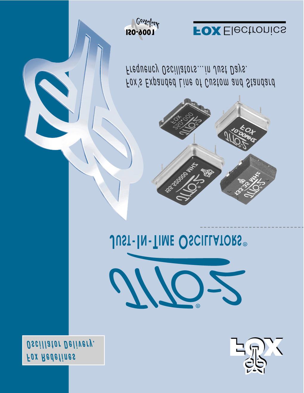
1 FOX ELECTRONICS VOLUME TWENTY F REQUENCY C ONTROL P RODUCTS CRYSTALS OSCILLATORS TCXOs VCXOs FILTERS

 as a resource for your special needs.")

2 The Fox Customer Technology Center Your Resource for Custom Crystal and Oscillator Development At Fox, we pride ourselves on offering the world's broadest range of standard, stocked, off-the-shelf crystals and oscillators. We also pride ourselves on knowing what the market needs. And we understand that, more and more, your applications may require a frequency control device with characteristics or capabilities that are not met by our standard offerings. That's why we've developed the Fox Customer Technology Center (CTC) as a resource for your special needs. Our new CTC is designed specifically to deliver cost-effective, fast-turn solutions to highly application-specific requirements for crystals, oscillators, TCXOs, VCXOs and OCXOs. Application Specific Crystals, Oscillators, TCXOs, VCXOs and OCXOs Cost-Effective Development with Rapid Turnaround Engineered Solutions from Minor Modifications to Full Custom Dedicated Engineering Support Team for Your Application Advanced Control Expertise from the World Leader tell you that, too and perhaps suggest another solution to the problem. Our application engineers are skilled at creating just the right solutions. If your application warrants it, we'll send a FOX FAE to your site to discuss the situation with you in person. The Fox CTC has already proven to be a tremendous success: several innovative products have already been developed by the CTC, including a 77 MHz TCXO, which was designed, developed, produced, tested and shipped in a matter of days rather than the four months quoted by our competitors!! From tweaks to full custom Engineered solutions for your application Your custom frequency control need may be for a slight modification to anexisting product a significant variation of a current product or an entirely new concept never before offered, but just what you need for your unique application. Whatever it takes, the FOX CTC is prepared to tackle it. We'll evaluate your need and provide a candid response on what it will take to meet that need. And, if we simply can't do it, we'll At the heart of the Fox CTC is a powerful, focused engineering capability, representing an integration and expansion of our design engineering and customer support resources, and a significantly expanded Field Application Engineering staff. The CTC specializes in the development of TCXOs, VCXOs and OCXOs over a wide range of frequencies and output structures not previously addressed. The CTC also employs patented technology for oscillator and RF applications up to.4 GHz, opening up new possibilities for highly engineered telecom and fiber optic products. The CTC is supported by a newly formed Design Central, comprising the Fox's DEN (Design Engineering Network) and the Fox Customer Application Team (CAT). The latter is a dedicated, multi-discipline team consisting of the primary customer service person, technical supervisor, design engineer and marketing person serving that particular customer. On the production side, the CTC has extensive manufacturing tools at its disposal, including an expanded range of thick and thin film, laser, pick and place, wire bonding and wafer handling processes. Our CTC is your resource! No matter how unique your frequency control need may be, chances are high that it can be met at the Fox Customer Technology Center. Call us with your problem or visit our CTC website at foxonline.com/ctc and we'll provide the solution!

3 M ISSION S TATEMENT TEMENT Fox Electronics' mission is to provide a broad line of frequency control products to worldwide electronics markets. Combining the disciplines of engineering, manufacturing, quality assurance, operations, information systems and marketing, Fox strives to provide its customers with superior quality, excellent service, leading edge products and knowledgeable application support. Regular updates and New Product Announcements are made on our web site. Visit Fox Electronics has a staff of application specialists ready to help you. Contact our hotline foxonline.com
4 CATALOG CONTENTS The FOX Mission... Contents FOX SERVICES Distributor Briefing... 4 Standard Microprocessor Crystals... 5 Standard Watch Crystals... 6 Standard Oscillators... 7 Standard TCXOs and VCXOs... 8 JITO-2 & FASTFOX Product Lines... 9 QUAR ARTZ CRYST STALS Quartz Crystal Selection Guide... 0 FX25B...2 x 2.5mm Ceramic SMD... FX52 Series...5 x.2mm Ceramic SMD... 2 FQA...6 x.5mm Ceramic Resin Sealed SMD... FMB...6 x.5mm Ceramic Seam Sealed SMD... 4 FE x 5mm Ceramic Resin Sealed SMD... 5 FD x 5mm Ceramic Seam Sealed SMD... 6 FC...8 x 5.5mm Ceramic Resin Sealed SMD... 7 FPX x 5mm Plastic Encased SMD... 8 HC49SD...2 x 4.8mm Resistance Weld SMD... 9 HC49S... x 4.6mm Resistance Weld Thru-Hole HC80U x 8.mm Resistance Weld Thru-Hole... 2 HC49U... x.5mm Resistance Weld Thru-Hole WATCH CRYST STALS FSX...7 x.5mm SMD Tuning Fork... 2 FSR x.7mm SMD Tuning Fork (Standard) NC Series...5 x 5mm / 2 x 6mm / x 8mm Thru-Hole Tuning Fork Crystal Part Description Guide SMD Crystals Tape And Reel Specifications CLOCK OSCILLATORS ORS Clock Oscillator Selection Guide Clock Oscillator General Characteristics Just-In-Time Oscillators (JITO -2) F50L Series...8V 5 x.2mm HCMOS Ceramic SMD with Standby... 6 F5L Series...2.5V 5 x.2mm HCMOS Ceramic SMD with Standby... 7 F50L Series...V 5 x.2mm HCMOS Ceramic SMD with Standby... 8 F4200 Series...V 6 x.5mm HCMOS Ceramic SMD with Standby... 9 F4500 Series...8V 7.5 x 5mm HCMOS SMD with Standby... F40 Series...2.5V 7.5 x 5mm HCMOS SMD with Standby... 4 F400 Series...V 7.5 x 5mm HCMOS SMD with Standby F45 Series...5.0V 7.5 x 5mm HCMOS/TTL SMD with Tri-State E/D F4600 Series...V 7.5 x 5mm LV-PECL Ceramic SMD with Comp. Output KFO Series...V/5.0V 2.8 x 9.8mm HCMOS/TTL Plastic SMD withtri-state E/D FSO Series...V/5.0V 4 x 9.8mm HCMOS/TTL Plastic SMD withtri-state E/D
5 F5C-2E / H5C-2E...V 4-Pin/8-Pin DIP HCMOS/TTL Thru-Hole w/ Tri-State E/D F5C-2E / H5C-2E...5.0V 4-Pin/8-Pin DIP HCMOS Thru-Hole with Tri-State E/D F00E...5.0V 4-Pin DIP TTL Thru-Hole F5L-4G...5.0V 4-Pin DIP PECL Thru-Hole... 5 Oscillator Part Description Guide Oscillator Tape and Reel Specifications... 5 VOL OLTAGE CONTROLLED OLLED CRYST STAL OSCILLATORS ORS (VCX CXO) VCXO, TCXO, and OCXO Selection Guide VCS25AXT...V 7.5 x 5mm HCMOS Ceramic SMD (Standard) VCSAXT Series....V 7.5 x 5mm HCMOS Ceramic SMD VCXO-D....V 4-Pin DIP HCMOS Thru-Hole VCXO-C V 4-Pin DIP HCMOS Thru-Hole TEMPERATURE TURE COMPENSATED CRYST STAL OSCILLATORS ORS (TCX CXO) FOX94 Series...0V 5 x.2mm Clipped-Sine Ceramic SMD FOX07H...0V 7.5 x 5mm Clipped-Sine Ceramic SMD FOX2BE...0V 7.5 x 5mm Clipped-Sine Ceramic SMD... 6 FOX80BE...0V.4 x 9.6mm Clipped-Sine FR-4 SMD FOX80 Series...0V/5.0V.4 x 9.6mm Clipped-Sine FR-4 SMD... 6 FOX78B...5.0V 4-Pin DIP Clipped-Sine Thru-Hole FOX V 4-Pin DIP HCMOS Thru-Hole OVEN CONTROLLED OLLED CRYST STAL AL OSCILLATORS ORS (OCXO) O) OCXO General Characteristics FTS50AH...V/5.0V 4-Pin DIP HCMOS Thru-Hole VCXO and TCXO Part Description Guide VCXO, TCXO, and OCXO Tape and Reel Specifications CRYST STAL AL FILTERS Monolithic Crystal Filters Standard Monolithic Crystal Filters... 7 Filters Part Description Guide TECHNICAL DATA Quartz Crystal Theory of Operation... 7 Quartz Crystal Design Notes Oscillator Theory of Operation Frequently Asked Questions CRYSTALS WATCH CRYSTALS OSCILLATORS VCXOs & TCXOs OCXOs FILTERS TECHNICAL
6 DISTRIBUTOR BRIEFING The Fox Distribution Program includes all of the Fox Part Numbers identified as DISTRIBUTOR STOCKING STANDARDS plus all of our JITO-2 product line. Fox franchised distributors maintain inventory of the STANDARDS to assure a constant supply to customers who design these items into their products. Of course, JITO-2 products are not maintained in inventory as they are 'built to order and schedule' for JIT delivery. This STANDARDS PROGRAM is formalized in our distributor relationship and in our Contract Manufacturing relationships, providing maximum global flexibility to our OEM customers. Design engineers can be confident that a STANDARD oscillator or crystal will be available for future manufacturing needs. A check with the Fox website will reveal current address and phone number information for all of the authorized distributors in your area. The feature "StockCheck" on Fox's home page ( may be used to confirm distributor inventory. Fox global distributors may have regional marketing centers in certain areas of the world, easily located through the distributors' website. Global Distribution North American Distribution European Distribution Eurosource MEV Elektronik Singapore Distribution Seamax sales@seamax.com.sg Australian Distribution Clarke & Severn 4
7 STANDARD CRYSTALS Inventory Support FOX STANDARD SPECIFICATIONS PARAMETER HC49U* 25 C ±0PPM Stability Operating Temperature Range-20 C ~ +70 C *Optional third lead, vinyl sleeves (HC49U only), and mylar spacer. ** Measurements are displayed in Millimeters. HC49S/49SD ±0PPM -20 C ~ +70 C FPX -0 C ~ +70 C FE -0 C ~ +60 C All specifications subject to change without notice.. Standard Packages Lowest Pricing Fox Quality Technical Support FREQ (MHz) CL pf 20pF 20pF 2pF 8pF SERIES 20pF SERIES 20pF 20pF 2pF 20pF SERIES 20pF 20pF SERIES 20pF 0pF 20pF SERIES 20pF SERIES 20pF SERIES 20pF SERIES SERIES 20pF SERIES 20pF SERIES 20pF 20pF SERIES 20pF 20pF 20pF 20pF 20pF SERIES 20pF SERIES 20pF SERIES 20pF SERIES 20pF 20pF 20pF 20pF 20pF 20pF 20pF 20pF 20pF 8pF 20pF 20pF HC49U FOX08S FOX020S FOX02S FOX024S FOX06S FOX068S FOX FOX0A FOX0 FOX FOX04 FOX044 FOX049 FOX FOX05A FOX060 FOX FOX06 FOX06-20 FOX07 FOX07-20 FOX080 FOX FOX08 FOX08-20 FOX092 FOX098 FOX FOX00 FOX00-20 FOX FOX-20 FOX5-20 FOX20 FOX20-20 FOX28-20 FOX4-20 FOX47-20 FOX60 FOX60-20 FOX84 FOX84-20 FOX96 FOX96-20 FOX200 FOX FOX22-20 FOX2F-20 FOX245F-20 FOX250F-20 FOX20-20 * FOX * FOX * FOX * FOX6-20 * ESR W MAX HC49S FOXS/06S FOXS/068S FOXS/ FOXS/0A FOXS/0 FOXS/ FOXS/04 FOXS/044 FOXS/049 FOXS/ FOXS/07 FOXS/07-20 FOXS/080 FOXS/ FOXS/08-20 FOXS/098 FOXS/ FOXS/00 FOXS/00-20 FOXS/-20 FOXS/5-20 FOXS/20 FOXS/20-20 FOXS/28-20 FOXS/4-20 FOXS/47-20 FOXS/60 FOXS/60-20 FOXS/84-20 FOXS/96-20 FOXS/200 FOXS/ FOXS/22-20 FOXS/2F-20 FOXS/245F-20 FOXS/250F-20 ESR W ESR W MAX Please Refer To Specification Sheets For Details HC49SD FOXSD/06S FOXSD/ FOXSD/0 FOXSD/04 FOXSD/044 FOXSD/ FOXSD/05A FOXSD/ FOXSD/07-20 FOXSD/ FOXSD/08-20 FOXSD/ FOXSD/00-20 FOXSD/-20 FOXSD/5-20 FOXSD/20-20 FOXSD/28-20 FOXSD/4-20 FOXSD/47-20 FOXSD/60-20 FOXSD/84-20 FOXSD/96-20 FOXSD/ FOXSD/22-20 FOXSD/2F-20 FOXSD/245F-20 FOXSD/250F-20 FOXSD/270F-20 FOXSD/20-20 * FOXSD/ * FOXSD/ * FOXSD/564-8 * FOXSD/ * FOXSD/6-20 * ESR W MAX FPX FPX06S FPX068S FPX FPX0A FPX0 FPX049 FPX FPX07 FPX07-20 FPX080 FPX FPX08-20 FPX FPX00 FPX00-20 FPX-20 FPX5-20 FPX20 FPX20-20 FPX28-20 FPX4-20 FPX47-20 FPX60 FPX60-20 FPX84-20 FPX96-20 FPX200 FPX FPX22-20 FPX2F-20 FPX245F-20 FPX250F-20 FPX20-20 * FPX * FPX * FPX * FPX6-20 * ESR W MAX FE ESR W MAX FE FE FE FE FE FE FE FE FE22-20 FE2F-20 FE245F-20 FE250F-20 * rd Overtone. "F" suffix denotes fundamental Rev. 05/0/02 5
8 STANDARD WATCH CRYSTALS FOX STANDARD SPECIFICATIONS PARAMETER Tolerance Stability Operating Temperature Range Load Capacitance Drive Level FSR khz ±20PPM PPM/( ºC) 2 - C ~ +85 C 2.5 pf.0 µw FOX STANDARD SPECIFICATIONS PARAMETER Tolerance Stability Operating Temperature Range Load Capacitance Drive Level NC khz ±20PPM PPM/( ºC) 2-20 C ~ +60 C 2.5 pf.0 µw FOX STANDARD SPECIFICATIONS PARAMETER Tolerance Stability Operating Temperature Range Load Capacitance Drive Level Rev. 05/0/02 NC khz ±20PPM PPM/( ºC) 2-20 C ~ +60 C 2.5 pf.0 µw 6
9 STANDARD OSCILLATORS DISTRIBUTOR STOCKING ITEMS Inventory Support Standard Packages Lowest Pricing Fox Quality Technical Support F00E / F5C-2E H5C-2E F45/F400/F405/F406 KFO90AT FOX STANDARD SPECIFICATIONS PARAMETER Voltage Stability Operating Temperature Range Output F00E 5V 00PPM 0ºC ~ +70ºC TTL F5C-2E 5V 0ºC ~ +70ºC HCMOS H5C-2E 5V 0ºC ~ +70ºC HCMOS KFO90AT 5V -0ºC ~ +70ºC HCMOS F45 5V -0ºC ~ +70ºC HCMOS F400.V -0ºC ~ +70ºC HCMOS F405/F406.V ±50 / ±25PPM -0ºC ~ +70ºC HCMOS FREQUENCY (MHz) Rev. 05/0/02 F00E F00E-00 F00E-08 F00E-020 F00E-024 F00E-068 F00E-0 F00E-060 F00E-07 F00E-080 F00E-00 F00E-5 F00E-20 F00E-4 F00E-47 F00E-60 F00E-84 F00E-200 F00E-2 F00E-250 F00E-20 F00E-0 F00E-480 F00E-500 F00E-6 F00E-800 F00E-000 F5C-2E F5C2E-080 F5C2E-00 F5C2E-20 F5C2E-60 F5C2E-200 F5C2E-2 F5C2E-250 F5C2E-20 F5C2E-0 H5C-2E F45 F400 F405 / F406 KFO90AT H5C2E-00 F45-08 F KFO-08 KFO-020 H5C2E-068 H5C2E-080 H5C2E-60 H5C2E-200 H5C2E-250 H5C2E-20 H5C2E-0 H5C2E-500 H5C2E-6 F F45-20 F45-4 F45-60 F F45-2 F F45-20 F45-0 F F F45-6 F F400-0 F F400-4 F F F F F F400- F400-0 F F F F F F405-4 F F F F405-0 F406-4 F F F F F KFO-0 KFO-080 KFO-00 KFO-20 KFO-4 KFO-60 KFO-200 KFO-2 KFO-20 KFO-0 KFO-480 KFO-500 KFO-600 KFO-6 KFO-666 JITO-2 JITO-2 JITO-2 JITO-2 JITO-2 JITO-2 JITO-2 JITO-2 JITO-2 JITO-2 JITO-2 JITO-2 JITO-2 JITO-2 JITO-2 JITO-2 JITO-2 JITO-2 JITO-2 JITO-2 JITO-2 JITO-2 JITO-2 JITO-2 JITO-2 JITO-2 JITO-2 JITO-2 JITO-2 JITO-2 JITO-2 JITO-2 7
10 STANDARD VCXOs & TCXOs DISTRIBUTOR STOCKING ITEMS FOX STANDARD SPECIFICATIONS PARAMETER VCS25AXT Supply Voltage.V Stability Pullability Operating Temperature Range -0 C ~ +70 C FOX80BE.0V ±2.5PPM ±.0PPM -0ºC ~ +75ºC VCS25AXT (VCXO) (MHz) Part Number VCS25AXT-0496 VCS25AXT-08 VCS25AXT-28 VCS25AXT-6 VCS25AXT-270 VCS25AXT-5 VCS25AXT-447 Other voltages, stabilities, and pullabilities available on custom order. Rev. 05/0/02 FOX80BE (VCTCXO) (MHz) Part Number FOX80BE-00 FOX80BE-28 FOX80BE-44 FOX80BE-60 FOX80BE-92 FOX80BE-200 The voltage control may be disabled by applying.50 volts to pin. Trimmerless and non-vc parts available on custom order. 8
11 PRODUCT LINE FAST DELIVERY SUPERIOR QUALITY CRYSTALS AND OSCILLATORS Let FASTFOX help you with all your "Rush" Requirements -888-GET-2-FOX Delivery: 5 to 0 working days Quartz Crystals HC49U ~ 27 MHz fundamental 0 ~ 60 MHz rd overtone HC49SD.579 ~ 64MHz Look for the Logo Oscillators F00E 4 ~ 25 MHz F5C-2E.000 ~ 50 MHz H5C-2E.000 ~ 50 MHz JITO-2 0. ~ 00 MHz for Fast Delivery Quotes: Call -888-GET-2-FOX for price and delivery confirmation. 9
12 CRYSTALS QUARTZ CRYSTAL SELECTION GUIDE SURFACE MOUNT CRYSTALS PRODUCT FX25B FX52 Series FQA FMB Range Tolerance Stability Temperature Range Key Features ~ MHz ±50 PPM ~ ±20 PPM ±50 PPM ~ ±20 PPM -0 C ~ +60 C to -ºC ~ +85ºC.2 x 2.5mm.0mm Height Max Low Cost to 50 MHz Resin Sealed or Seam Sealed 00 ~ MHz ±50 PPM ~ ±0 PPM ±50 PPM ~ ±0 PPM -0 C ~ +60 C to -ºC ~ +85ºC 5 x.2mm.0mm Height Max to 67 MHz Low Cost Resin Sealed or Seam Welded.0592 ~ MHz ±50 PPM ~ ±20 PPM ±00 PPM ~ ±20 PPM -0 C ~ +60 C to -ºC ~ +85ºC 6 x.5mm.4mm Height Max Low Cost - Resin Sealed to MHz 0.68 ~ MHz ±50 PPM ~ ±5 PPM ±00 PPM ~ ± PPM -0 C ~ +60 C to -ºC ~ +85ºC 6 x.5mm.mm Height Max to 67 MHz Seam Sealed Catalog Pages Page Page 2 Page Page 4 PRODUCT FE FD FC FPX HC49SD Range Tolerance Stability Temperature Range Key Features Stocking Std ~ MHz ±50 PPM ~ ±20 PPM ±50 PPM ~ ±5 PPM -0 C ~ +60 C to -ºC ~ +85ºC 7.5 x 5mm.4mm Height Max Low Cost - Resin Sealed to 50 MHz 2 Additional Footprints (FH, FL) ~ MHz ±50 PPM ~ ±5 PPM ±50 PPM ~ ± PPM -0 C ~ +60 C to -ºC ~ +85ºC 7.5 x 5mm.mm Height Max to 50 MHz Seam Sealed.200 ~ MHz ±50 PPM ~ ±20 PPM ±50 PPM ~ ±5 PPM -0 C ~ +60 C to -ºC ~ +85ºC.8 x 5.5mm 2.5mm Height Max Low Cost - Resin Sealed Stocking Std ~ MHz ±50 PPM ~ ±20 PPM ±00 PPM ~ ±20 PPM -0 C ~ +60 C to -ºC ~ +85ºC Low Cost Plastic Encapsulated Stocking Std..200 ~ MHz ±50 PPM ~ ±0 PPM ±50 PPM ~ ±5 PPM -0 C ~ +60 C to -ºC ~ +85ºC Low Cost to 50 MHz Catalog Pages Page 5 Page 6 Page 7 Page 8 Page 9 THRU-HOLE CRYSTALS / WATCH CRYSTALS PRODUCT HC49S HC80U HC49U WATCH CRYSTALS Stocking Std. Stocking Std. Range Tolerance Stability Temperature Range Key Features.200 ~ MHz ±50 PPM ~ ±0 PPM ~ ±5 PPM -0 C ~ +70 C to -ºC ~ +85ºC.6mm Profile Low Cost Resistance Weld to 50 MHz ~ MHz ±0 PPM ~ ±5 PPM ±50 PPM ~ ± PPM -20 C ~ +70 C to -ºC ~ +70ºC High Range to 50 MHz.842 ~ MHz ±0 PPM ~ ±5 PPM ±50 PPM ~ ± PPM -20 C ~ +70 C to -ºC ~ +85ºC Low Cost to MHz khz ±20PPM -0.04PPM / ( C) 2-20 C ~ +60 C / -ºC ~ +85ºC Miniature Pkgs. Long Term Stability Catalog Pages Page 20 Page 2 FASTFOX is a quick delivery service. Check with Fox Customer Service for available frequencies. Page 22 Pages 2-25 IMPORTANT When ordering any non-standard crystals, please specify series or parallel resonance. If parallel, the load capacitance (CL) needs to be specified in picofarads pf. 0
13 CERAMIC SMD CRYSTAL FX25B Low Cost to 50 MHz Tape and Reel (,000 pcs. STD) OPTIONS Tolerances to < 20 PPM Stabilities to < 20 PPM Temperatures to -ºC ~ +85ºC 0.8mm Height Max CRYSTALS STANDARD SPECIFICATIONS Range 25ºC Stability, 25ºC Over Operating Temp Range Temperature Range Operating (TOPR) Storage (TSTG) Equivalent Series Resistance Shunt Capacitance (Co) Load Capacitance (CL) Drive Level Aging per year ~ MHz ±50 PPM ±50 PPM -0ºC ~ +60ºC -ºC ~ +85ºC 90 Ω 7.0 pf 0 pf ~ Series (Customer Specified) 0. mw ±5 PPM Other tolerances, stabilities & operating temperature ranges available. Consult Fox Customer Service for specific requirements. All specifications subject to change without notice. Rev. 05/0/02 See page 27 for tape and reel specifications.
14 CRYSTALS CERAMIC SMD CRYSTALS FX52 SERIES Low Cost to 67 MHz Resin Sealed or Seam Sealed Tape and Reel (2,000 pcs. STD) OPTIONS Tolerances to < 0 PPM Stabilities to < 0 PPM Temperatures to -ºC ~ +85ºC STANDARD SPECIFICATIONS Range Tolerance, Ta=25ºC 00 ~.000 MHz.000+ ~ MHz Stability 00 ~.000 MHz 25ºC).000+ ~ MHz Temperature Range Operating (TOPR) Storage (TSTG) Shunt Capacitance (Co) Load Capacitance (CL) Drive Level Aging per year 00 ~ MHz See Stability ±50 PPM ±00 PPM 2-0ºC ~ +60ºC -ºC ~ +85ºC 7.0 pf 0 pf ~ Series (Customer Specified) 0. mw ±5 PPM Other tolerances, stabilities & operating temperature ranges available. Consult Fox Customer Service for specific requirements. 2 Inclusive of tolerance at 25ºC All specifications subject to change without notice. Rev. 05/0/02 Range (MHz) 00 ~ ~ ~ Operating Mode Max ESR W See page 27 for tape and reel specifications.
15 CERAMIC RESIN SEALED SMD CRYSTAL FQA Low Cost to MHz Resin Sealed Tape and Reel (2,000 pcs. STD) OPTIONS Tolerances to < 20 PPM Stabilities to < 20 PPM Temperatures to -ºC ~ +85ºC CRYSTALS STANDARD SPECIFICATIONS Range Stability Over Operating Temp Range Temperature Range Operating (TOPR) Storage (TSTG) Shunt Capacitance (Co) Load Capacitance (CL) Drive Level Aging per year.0592 ~ MHz ±00 PPM 2-0ºC ~ +60ºC -ºC ~ +85ºC 7.0 pf 0 pf ~ Series (Customer Specified) 0. mw ±5 PPM Other stabilities & operating temperature ranges available. Consult Fox Customer Service for specific requirements. 2 Inclusive of tolerance at 25ºC. All specifications subject to change without notice. Rev. 05/0/02 Range (MHz).0592 ~ ~ ~ ~ Operating Mode rd OT Max ESR W See page 27 for tape and reel specifications.
 OPTIONS Tolerances to < 5 PPM Stabilities to < PPM Temperatures to -ºC ~ +85ºC STANDARD SPECIFICATIONS Range Stability Over Operating Temp Range Temperature Range Operating (TOPR) Storage (TSTG)")

16 CRYSTALS CERAMIC SEAM SEALED SMD CRYSTAL FMB to MHz Seam Sealed Tape and Reel (2,000 pcs. STD) OPTIONS Tolerances to < 5 PPM Stabilities to < PPM Temperatures to -ºC ~ +85ºC STANDARD SPECIFICATIONS Range Stability Over Operating Temp Range Temperature Range Operating (TOPR) Storage (TSTG) Shunt Capacitance (Co) Load Capacitance (CL) Drive Level Aging per year 0.68 ~ MHz ±00 PPM 2-0ºC ~ +60ºC -ºC ~ +85ºC 7.0 pf 0 pf ~ Series (Customer Specified) 0. mw ±5 PPM Other tolerances, stabilities & operating temperature ranges available. Consult Fox Customer Service for specific requirements. 2 Inclusive of tolerance at 25ºC. All specifications subject to change without notice. Rev. 05/0/02 Range (MHz) 0.68 ~ ~ ~ ~ Operating Mode rd OT Max ESR W See page 27 for tape and reel specifications.
 OPTIONS Tolerances to < 20 PPM Stabilities to < 5 PPM Temperatures to -ºC ~ +85ºC.")
17 CERAMIC RESIN SEALED SMD CRYSTAL FE Low Cost High Range to 50 MHz (BT Cut) Resin Sealed Tape and Reel (2,000 pcs. STD) OPTIONS Tolerances to < 20 PPM Stabilities to < 5 PPM Temperatures to -ºC ~ +85ºC.4mm Height Max 2 Additional Footprints (FH, FL) CRYSTALS STANDARD SPECIFICATIONS Range 25ºC Stability, 25ºC Over Operating Temp Range Temperature Range Operating (TOPR) Storage (TSTG) Shunt Capacitance (Co) Load Capacitance (CL) Drive Level Aging per year 7.24 ~ MHz ±50 PPM -0ºC ~ +60ºC -ºC ~ +85ºC 7.0 pf 0 pf ~ Series (Customer Specified) 0.5 mw ±5 PPM Other stabilities & operating temperature ranges available. Consult Fox Customer Service for specific requirements. All specifications subject to change without notice. Rev. 05/0/02 Range (MHz) 7.24 ~ ~ ~ ~ ~ Operating Mode rd OT 5th OT Max ESR W See page 27 for tape and reel specifications. 5
 OPTIONS Tolerances to < 5 PPM Stabilities to < PPM Temperatures to -ºC ~ +85ºC STANDARD SPECIFICATIONS Range Tolerance @ 25ºC Stability, ref @ 25ºC Over Operating Temp Range Temperature Range")
18 CRYSTALS CERAMIC SEAM SEALED SMD CRYSTAL FD High Range to 50 MHz (BT Cut) Seam Sealed Tape and Reel (,000 pcs. STD) OPTIONS Tolerances to < 5 PPM Stabilities to < PPM Temperatures to -ºC ~ +85ºC STANDARD SPECIFICATIONS Range 25ºC Stability, 25ºC Over Operating Temp Range Temperature Range Operating (TOPR) Storage (TSTG) Shunt Capacitance (Co) Load Capacitance (CL) Drive Level Aging per year ~ MHz ±50 PPM ±50 PPM -0ºC ~ +60ºC -ºC ~ +85ºC 7.0 pf 0 pf ~ Series (Customer Specified) 0.5 mw ±5 PPM Other tolerances, stabilities & operating temperature ranges available. Consult Fox Customer Service for specific requirements. All specifications subject to change without notice. Rev. 05/0/02 Range (MHz) ~ ~ ~ ~ Operating Mode rd OT 5th OT Max ESR W See page 27 for tape and reel specifications.
19 CERAMIC RESIN SEALED SMD CRYSTAL FC Low Cost Resin Sealed Tape and Reel (,000 pcs. STD) OPTIONS Tolerances to < 20 PPM Stabilities to < 5 PPM Temperatures to -ºC ~ +85ºC CRYSTALS STANDARD SPECIFICATIONS Range 25ºC Stability, 25ºC Over Operating Temp Range Temperature Range Operating (TOPR) Storage (TSTG) Shunt Capacitance (Co) Load Capacitance (CL) Drive Level Aging per year All specifications subject to change without notice. Rev. 05/0/ ~ MHz ±50 PPM ±50 PPM -0ºC ~ +60ºC -ºC ~ +85ºC 7.0 pf 0 pf ~ Series (Customer Specified) 0. mw ±5 PPM Range (MHz).200 ~ ~ ~ ~ ~ ~ ~ Operating Mode Max ESR W See page 27 for tape and reel specifications. 7
20 CRYSTALS PLASTIC ENCASED SMD CRYSTAL FPX Low Cost Stocking Standard Plastic Encapsulated Tape and Reel (,000 pcs. STD) OPTIONS Tolerances to < 20 PPM Stabilities to < 20 PPM Temperatures to -ºC ~ +85ºC Alternate Metal Can Package (HC49SPX) STANDARD SPECIFICATIONS Range 25ºC Stability, 25ºC Over Operating Temp Range Temperature Range Operating (TOPR) Storage (TSTG) Shunt Capacitance (Co) Load Capacitance (CL) Drive Level Aging per year ~ MHz ±50 PPM ±00 PPM -0ºC ~ +70ºC -55ºC ~ +25ºC 7.0 pf 0 pf ~ Series (Customer Specified) 0. mw ±5 PPM Other tolerances, stabilities & operating temperature ranges available. Consult Fox Customer Service for specific requirements. All specifications subject to change without notice. Rev. 05/0/02 Range (MHz).579 ~ ~ ~ ~ ~ ~ ~ ~ ~ Operating Mode rd OT Max ESR W See page 27 for tape and reel specifications.
21 RESISTANCE WELD SMD CRYSTAL HC49SD OPTIONS Low Cost Tolerances to < 0 PPM Stock Standard Stabilities to < 5 PPM to 50 MHz (BT Temperatures to -ºC ~ -85ºC Cut) 4 Pad HC49SPX (Alternate to Tape and Reel (,000 pcs. STD) FPX).2mm Height Max (HC49SSD) CRYSTALS STANDARD SPECIFICATIONS Range 25ºC Stability, 25ºC Over Operating Temp Range Temperature Range Operating (TOPR) Storage (TSTG) Shunt Capacitance (Co) Load Capacitance (CL) Drive Level 25ºC; per year.200 ~ MHz ±50 PPM ±50 PPM -0ºC ~ +70ºC -ºC ~ +85ºC 7.0 pf 0 pf ~ Series (Customer Specified) 0.5 mw ±5 PPM Other tolerances, stabilities & operating temperature ranges available. Consult Fox Customer Service for specific requirements. All specifications subject to change without notice. Rev. 05/0/02 Range (MHz).200 ~ ~ ~ ~ ~ ~ ~ ~ ~ ~ Operating Mode rd OT Max ESR W See page 27 for tape and reel specifications. 9
22 CRYSTALS RESISTANCE WELD THRU-HOLE CRYSTAL HC49S Low Cost Stocking Standard to 50 MHz (BT Cut) Resistance Weld OPTIONS Tolerances to < 0 PPM Stabilities to < 5 PPM Temperatures to -ºC ~ +85ºC 2.5mm Height Max (HC49SS) STANDARD SPECIFICATIONS Range 25ºC Stability, 25ºC Over Operating Temp Range Temperature Range Operating (TOPR) Storage (TSTG) Shunt Capacitance (Co) Load Capacitance (CL) Drive Level Aging per year.200 ~ MHz ±50 PPM ±50 PPM -20ºC ~ +70ºC -ºC ~ +85ºC 7.0 pf 0 pf ~ Series (Customer Specified) 0.5 mw ±5 PPM Other tolerances, stabilities & operating temperature ranges available. Consult Fox Customer Service for specific requirements. All specifications subject to change without notice. Rev. 05/0/02 Range (MHz).200 ~ ~ ~ ~ ~ ~ ~ ~ ~ ~ Operating Mode rd OT Max ESR W
23 RESISTANCE WELD THRU-HOLE CRYSTAL HC80U High Range to 50 MHz Resistance Weld OPTIONS Tolerances to < 5 PPM Stabilities to < PPM Temperatures to -ºC ~ -85ºC SMD Gullwing (HC80UW) CRYSTALS STANDARD SPECIFICATIONS Range 25ºC Stability, 25ºC Over Operating Temp Range Temperature Range Operating (TOPR) Storage (TSTG) Shunt Capacitance (Co) Load Capacitance (CL) Drive Level Aging per year ~ MHz ±0 PPM ±50 PPM -20ºC ~ +70ºC -ºC ~ +85ºC 7.0 pf 0 pf ~ Series (Customer Specified).0 mw ± PPM Other tolerances, stabilities & operating temperature ranges available. Consult Fox Customer Service for specific requirements. All specifications subject to change without notice. Rev. 05/0/02 Range (MHz) ~ ~ ~ ~ ~ ~ ~ ~ ~ ~ ~ Operating Mode rd OT 5th OT 7th OT Max ESR W
24 CRYSTALS RESISTANCE WELD THRU-HOLE CRYSTAL HC49U Low Cost Stocking Standard High Range to MHz Resistance Weld OPTIONS Tolerances to < 5 PPM Stabilities to < PPM Temperatures to -ºC ~ -85ºC Mylar Spacer Vinyl Sleeve Third Lead SMD Gullwing (HC49UW) STANDARD SPECIFICATIONS Range 25ºC Stability, 25ºC Over Operating Temp Range Temperature Range Operating (TOPR) Storage (TSTG) Shunt Capacitance (Co) Load Capacitance (CL) Drive Level.842 ~.000 MHz.000+ ~ MHz Aging per year.842 ~ MHz ±0 PPM ±50 PPM -20ºC ~ +70ºC -ºC ~ +85ºC 7.0 pf 0 pf ~ Series (Customer Specified) mw.0 mw ±5 PPM Other tolerances, stabilities & operating temperature ranges available. Consult Fox Customer Service for specific requirements. All specifications subject to change without notice. Rev. 05/0/02 Range (MHz).842 ~ ~ ~ ~ ~ ~ ~ ~ ~ ~ ~ ~ ~ ~ ~ ~ ~ Operating Mode rd OT 5th OT 7th OT Max ESR W
25 SMD TUNING FORK FSX Extremely Small Size Low Cost.4mm Height Max Tape and Reel (,000 pcs. STD) WATCH CRYSTALS STANDARD SPECIFICATIONS Range 25ºC Stability, 25ºC Temperature Range Operating (TOPR) Storage (TSTG) Equivalent Series Resistance Load Capacitance (CL) Insulation 00VDC Drive Level Aging All specifications subject to change without notice. Rev. 05/0/ khz ±20 PPM -0.04PPM/( ºC) 2 -ºC ~ +85ºC -ºC ~ +85ºC 65 kω 7 pf, 2.5pF 500 MΩ 0. µw ± PPM See page 27 for tape and reel specifications. 2
26 WATCH CRYS- TALS SMD TUNING FORK FSR27 Miniature Package 2.5mm Height Long Term Stability Tape and Reel (,000 pcs. STD) STANDARD SPECIFICATIONS 25ºC Stability Temperature Coefficient Temperature Range Turnover (TO) Operating (TOPR) Storage (TSTG) Equivalent Series Resistance (RS) Load Capacitance (CL) Insulation 00VDC Drive Level Aging per year All specifications subject to change without notice. Rev. 05/0/ khz ±20 PPM PPM / ( ºC) 2 +20ºC ~ +0ºC -ºC ~ +85ºC -55ºC ~ +25ºC 50 kω 2.5 pf (Standard) 6 pf (Optional) 500 MΩ.0 µw ± PPM 24 See page 27 for tape and reel specifications.
 Operating (TOPR) Storage (TSTG) Equivalent Series Resistance (RS) NC5 / NC26 NC8 Load Capacitance (CL) Insulation Resistance @ 00VDC Drive Level Aging per")
27 WATCH CRYS- TALS THRU-HOLE TUNING FORK NC5/NC26/NC8 Miniature Packages Low Cost Cold Weld Design Long Term Stability Tight Tolerance STANDARD SPECIFICATIONS 25ºC Stability Temperature Coefficient Temperature Range Turnover (TO) Operating (TOPR) Storage (TSTG) Equivalent Series Resistance (RS) NC5 / NC26 NC8 Load Capacitance (CL) Insulation 00VDC Drive Level Aging per year All specifications subject to change without notice. Rev. 05/0/ khz PPM / ( ºC) 2 +20ºC ~ +0ºC -20ºC ~ +60ºC -0ºC ~ +70ºC 50 kω 5 kω 2.5 pf (Standard) 6 pf (Optional) 500 MΩ.0 µw ± PPM 25
28 Fox Electronics Part Description Guide for Crystals Make Selection from Product Family in Fox Catalog or Foxonline.com For Example: HC49SD Fox Production SMD Reel Quantities FD K FE/FH/FL 2K FC K FM/FMB 2K FPX K FSM 2K HC49SD K HC49SSD K FST/FSR K FQA 2K FSX K FX25 K FX52A 2K (####.######) 2 MHz Customer Fills In Section A A ± 00ppm B ± 50 ppm C ± 0ppm D ± 25ppm E ± 20ppm F ± 5ppm G ± 2ppm H ± 0ppm J ± 7.5ppm K ± 7ppm L ± 5ppm M ± 4ppm N ± ppm P ± 2.5ppm R ± 2ppm S ±.5ppm T ± ppm U ± 0.5ppm V ± 200ppm W ± 70ppm X ± 00ppm OVERALL Y ± 000ppm Z ± Other Tolerance 2 Pick from Section A 4 Stability 2 Pick from Section A Operating Temp. Range A = 0º to +50ºC C = 0º to +70ºC B = -0º to +50ºC D = -0º to +60ºC E = -0º to +70ºC F = -20º to +70ºC Z = -20º to +75ºC G = -0º to +70ºC H = -0º to +75ºC J = -0º to +80ºC K = -0º to +85ºC L = -5º to +80ºC V = -5º to +85ºC M = -º to +85ºC N = -º to +90ºC P = -º to +05ºC U = -55º to +85ºC R = -55º to +00ºC S = -55º to +05ºC T = -55º to +25ºC W = Other 5 Operating Temp 2 Circuit Condition 000 = Series 060 = 6pF 075 = 7.5pF 080 = 8pF 00 = 0pF 05 = 0.5pF 20 = 2pF 25 = 2.5pF 0 = pf 50 = 5pF 60 = 6pF 80 = 8pF 200 = 20pF 220 = 22pF 2 = 24pF 270 = 27pF 00 = 0pF 20 = 2pF 0 = pf 500 = 50pF 999 = Other 6 Circuit Condition Notes: Fox unique part numbers for non-standards are randomly generated based on the elements of the part description in a format: ### - - Random # ( is Fox unique part number). 2 All combinations are not possible. * 0 = Tape/Reel assumes that no quantity per reel was specified: therefore, the Fox Production SMD Reel Quantities list applies. For any other quantities specified a broken reel charge will apply. 7 Oscillation Mode Oscillation Mode SMD Packaging 0 = Tape/Reel* = 250 = 250 = rd Overtone 500 = = 5th Overtone 000 = = 7th Overtone Tape Only = Tape Only 9 = 9th Overtone 0 = BT Cut Value Added 8 SMD Packaging 9 Fox Use 0/ Value Added Custom A = rd LEAD Soldered B = rd LEAD Welded C = rd Base Lead D = Sleeve E = Flat Spacer F = Ribbed Spacer L = Formed Leads M = Special Marking N = Cut Base P = Cut Top S = Bulk T = Trays V = Radial Tape/Straight W = Radial Tape/Crimp Y = Filter Box Z = SMD Tape Z8 = SMD 8mm Tape (FPX Only) Z2 - SMD 2mm Tape (FPX and FPX Rev. C 2 Custom C = Custom Please attach drawing and/or additional electrical specs for our engineering department. 26
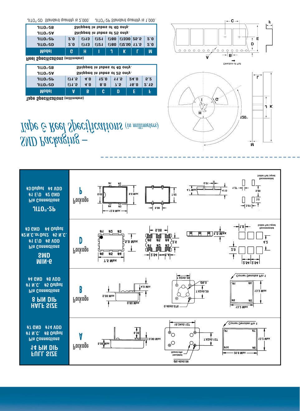
29 SURFACE MOUNT CRYSTALS TAPE AND REEL SPECIFICATIONS TAPE SPECIFICATIONS (millimeters) MODEL FX25B FX52 Series FQA FMB FE FD FC FPX HC49SD FSX FSR A B C D E F STD QTY,000,000 / 2,000 2,000 2,000 2,000,000,000 2,000,000,000,000 Standard reel quantity. REEL SPECIFICATIONS (millimeters) MODEL FX25B FX52 Series FQA FMB FE FD FC FPX HC49SD FSX FSR G H I J /00 K / L M.2 27
30 CLOCK OSCILLATOR SELECTION GUIDE JITO -2 AND SURFACE MOUNT OSCILLATORS PRODUCT JITO -2 F50L/F5L Series F50L Series F4200 Series Full Size 4 PIN DIP Half Size 8 PIN DIP MIN-6 JITO-2P Surface Mount Plastic OSCILLATORS Range Stability Temperature Range Key Features Catalog Pages 0.44 ~ MHz,, ±0PPM, ±25PPM, ±20PPM -20 C ~ +70 C and -ºC ~ +85ºC Custom and Standard Frequencies. or 5 Volts, HCMOS or PECL SMD and Thru-Hole packages available Delivery in 0 days or less! Pages 0-5 SURFACE MOUNT OSCILLATORS.800 ~ MHz ±00, ±50, ±25, ±20 PPM -0ºC ~ +70ºC - C ~ +85 C (Option) 5 x.2mm.8v / 2.5V Operation HCMOS Low Current Standby Function (0µA MAX) Pages 6 & ~ MHz ±00, ±50, ±25, ±20 PPM -0ºC ~ +70ºC - C ~ +85 C (Option) 5 x.2mm.v Operation HCMOS Low Current Standby Function (0µA MAX) Page ~ MHz ±00, ±50, ±25, ±20 PPM -0ºC ~ +70ºC - C ~ +85 C (Option) 6 x.5mm.v Operation HCMOS Low Current Standby Function (0µA MAX) Page 9 PRODUCT F4500/F40 Series F400 Series F45 Series F4600 Series Range Stability Temperature Range Key Features.800 ~ MHz ±00, ±50, ±25, ±20 PPM -0ºC ~ +70ºC - C ~ +85 C (Option) 7.5 x 5mm.8V / 2.5V Operation HCMOS Low Current Standby Function (0µA MAX).000 ~ MHz ±00, ±50, ±25, ±20 PPM -0ºC ~ +70ºC - C ~ +85 C (Option) 7.5 x 5mm.V Operation HCMOS Low Current Standby Function (0µA MAX) Stocking Std. Stocking Std..000 ~ MHz ±00, ±50, ±25, ±20 PPM -0ºC ~ +70ºC - C ~ +85 C (Option) 7.5 x 5mm 5.0V Operation HCMOS/TTL Tri-State E/D ~ MHz ±00, ±50, ±25, ±20 PPM -0ºC ~ +70ºC - C ~ +85 C (Option) 7.5 x 5mm.V Operation LV-PECL E/D Function Catalog Pages Pages & 4 Page 42 & 4 Page 44 Page 45 SURFACE MOUNT AND THRU-HOLE OSCILLATORS PRODUCT FSO Series KFO Series F5C-2E / H5C-2E F5C-2E / H5C-2E F00E Range Stability Temperature Range Key Features.000 ~ MHz ±200, ±00, ±50 PPM -0ºC ~ +70ºC - C ~ +85 C (±200 PPM Option) 4 x 9.8mm 5.0V /.V HCMOS/TTL Tri-State E/D.500 ~ MHz ±00, ±50 PPM -0ºC ~ +70ºC -ºC ~ +85ºC (Option) 2.8 x 9.8mm 5.0V /.V HCMOS/TTL Tri-State E/D Stocking Std..000 ~ MHz ±00, ±50, ±25, ±20 PPM 0ºC ~ +70ºC -ºC ~ +85ºC (Option) 4-Pin / 8-Pin DIP 5.0V HCMOS/TTL Tri-State E/D Stocking Std..000 ~ MHz ±00, ±50, ±25, ±20 PPM 0ºC ~ +70ºC -ºC ~ +85ºC (Option) 4-Pin / 8-Pin DIP.V HCMOS/TTL Tri-State E/D.000 ~ MHz ±00, ±50, ±25, ±20 PPM 0ºC ~ +70ºC -ºC ~ +85ºC (Option) 4-Pin / 8-Pin DIP 5.0V TTL Stocking Std. Catalog Pages Pages 46 Page 47 Page 48 Page 49 Page 50 28
31 OSCILLATORS CLOCK OSCILLATOR GENERAL CHARACTERISTICS MECHANICAL SPECIFICATIONS Gross Leak Test Hermetically Sealed Package Seal Strength (Thru-Hole) Bend Test (Pin Material) Solvent Resistance Marking Ink Solderability Maximum Soldering Temp. Reliability Tests: Shock, Vibration, Aging (Burn-in), Temperature Cycle. All specifications subject to change without notice. Rev. 05/0/00 All units 00% leak tested. Mass spectrometer leak rate less than 2 x 0-8 Atm. CC/sec. of helium. 2.27Kg max. force perpendicular to top and bottom. Will withstand maximum bend of 90, referenced to base, for 2 bends. (Iron and Nickel - Nickel coated, solder dipped.) Isopropyl Alcohol, Trichloroethane Note - Ultrasonic cleaning not to be used. Note 2 - Unit can be cleaned in only one solvent listed. Epoxy, heat cured or UV cured (ceramic SMD) The terminals are considered solderable and acceptable for electrical connection if 95% of the cooled solder surface is uniform and free from breaks and pinholes. The other 5% of the cooled solder surface may show only pinholes, voids, or rough spots that are not concentrated in one area. 270 C for 0 seconds on leads. 29
32
33
34
35

36
37
 MODEL NUMBER SELECTION Model Number F0 F0R F5 F5R F6 F8 Stability ±25PPM ±20PPM Operating Temperature (ºC) Range (MHz).800 ~ 50.")
.800 ~ 50.000 MHz -55ºC ~ +25ºC.V ± 0% 20mA 25mA Output Symmetry (50% VDD).000 ~ 50.")
38 .V HCMOS SMD OSCILLATOR WITH STANDBY F0 SERIES.V Operation HCMOS Output Standby Function Tape and Reel (2,000 pcs. STD) MODEL NUMBER SELECTION Model Number F0 F0R F5 F5R F6 F8 Stability ±25PPM ±20PPM Operating Temperature (ºC) Range (MHz).800 ~ ~ ~ ~ ~ ~ ELECTRICAL CHARACTERISTICS Range (FO) Storage Temperature Range Supply Voltage (VDD) Input Current (IDD).800 ~ 00 MHz 00+ ~ MHz (TSTG).800 ~ MHz -55ºC ~ +25ºC.V ± 0% 20mA 25mA Output Symmetry (50% VDD).000 ~ MHz 45% ~ 55% Rise Time (0% ~ 90% VDD) (TR) Fall Time (90% ~ 0% VDD) (TF) Output Voltage (VOL) Output Current (VOH) (IOL) (IOH) Output Load (HCMOS) Standby Current (VIL 0.99V) Start-up Time (TS) Output Disable Time 2 Output Enable Time 2 6nS 6nS 0% VDD 90% VDD Min 2mA Min -2mA Min 5pF 0µA 5mS 50nS 5mS Inclusive of 25ºC tolerance, operating temperature range, input voltage change, load change, aging, shock, and vibration. An internal pullup resistor from pin to pin 4 allows active output if pin is left open. See page 29 for mechanical specifications, test circuits, and output waveform. Note: A 0.0µF bypass capacitor should be placed between VDD (Pin 4) and GND (Pin 2) to minimize power supply line noise. All specifications subject to change without notice. Rev. 0/0/02 ENABLE / DISABLE FUNCTION 2 INH (Pin ) OUTPUT (Pin ) OPEN ACTIVE '' Level VIH 2. V ACTIVE '0' Level VIL 0.99 V High Z See page 5 for tape and reel specifications.
39 .8V HCMOS CERAMIC SMD OSCILLATOR WITH STANDBY F50L SERIES.8V Operation HCMOS Output Low Power Consumption Standby Function Tape and Reel (,000 or 2,000 pcs. STD) OSCILLATORS MODEL NUMBER SELECTION Model Number F50L F50LR F55L F55LR F56L F56LR F58L Stability ±25PPM ±25PPM ±20PPM Operating Temperature (ºC) Range (MHz).800 ~ ~ ~ ~ ~ ~ ~ ELECTRICAL CHARACTERISTICS Range (FO) Storage Temperature Range Supply Voltage (VDD) Input Current (IDD).800 ~ 2.00 MHz ~ MHz Output Symmetry (50% VDD) Rise Time (20% ~ 80% VDD) (TR).800 ~ 2.00 MHz ~ MHz Fall Time (80% ~ 20% VDD) (TF).800 ~ 2.00 MHz ~ MHz Output Voltage (VOL) Output Current (VOH) (IOL) (IOH) Output Load (HCMOS) Standby Current Start-up Time (TS) Output Disable Time 2 Output Enable Time 2 (TSTG).800 ~ MHz -55ºC ~ +25ºC.8V ± 5% 7mA 5mA % ~ 60% 5nS.5nS 5nS.5nS 20% VDD 80% VDD Min 2mA Min 2mA Min 5pF 0µA 0mS 00nS 0mS Inclusive of 25ºC tolerance, operating temperature range, input voltage change, load change, aging, shock, and vibration. See page 29 for mechanical specifications, test circuits, and output waveform. All specifications subject to change without notice. Rev. 05/0/02 6 ENABLE / DISABLE FUNCTION 2 INH (Pin ) OUTPUT (Pin ) OPEN ACTIVE '' Level VIH 0.7 V ACTIVE '0' Level VIL 0. V High Z See page 5 for tape and reel specifications.
40 OSCILLATORS 2.5V HCMOS CERAMIC SMD OSCILLATOR WITH STANDBY F5L SERIES 2.5V Operation HCMOS Output Low Power Consumption Standby Function Tape and Reel (,000 or 2,000 pcs. STD) MODEL NUMBER SELECTION Model Number F5L F5LR F545L F545LR F546L F546LR F548L Stability ±25PPM ±25PPM ±20PPM Operating Temperature (ºC) Range (MHz).800 ~ ~ ~ ~ ~ ~ ~ ELECTRICAL CHARACTERISTICS Range (FO) Storage Temperature Range Supply Voltage (VDD) Input Current (IDD) (TSTG).800 ~ MHz -55ºC ~ +25ºC 2.5V ± 5%.800 ~ 2.00 MHz 0mA ~ MHz 2mA Output Symmetry (50% VDD) 45% ~ 55% Rise Time (0% ~ 90% VDD) (TR) 5nS Fall Time (90% ~ 0% VDD) (TF) 5nS Output Voltage (VOL) 0% VDD (VOH) 90% VDD Min Output Current (IOL) 4mA Min (IOH) 4mA Min Output Load (HCMOS) 5pF Standby Current 0µA Start-up Time (TS) 0mS Output Disable Time 2 50nS Output Enable Time 2 0mS Inclusive of 25ºC tolerance, operating temperature range, input voltage change, load change, aging, shock, and vibration. See page 29 for mechanical specifications, test circuits, and output waveform. All specifications subject to change without notice. Rev. 05/0/02 ENABLE / DISABLE FUNCTION 2 INH (Pin ) OUTPUT (Pin ) OPEN ACTIVE '' Level VIH 0.7 V ACTIVE '0' Level VIL 0. V High Z See page 5 for tape and reel specifications. 7
41 .V HCMOS CERAMIC SMD OSCILLATOR WITH STANDBY F50L SERIES OPTIONS.V Operation 5.0V (F550L) Version HCMOS Output Available Standby Function Tape and Reel (,000 or 2,000 pcs. STD) OSCILLATORS MODEL NUMBER SELECTION Model Number F50L F50LR F55L F55LR F56L F56LR F58L Stability ±25PPM ±25PPM ±20PPM Operating Temperature (ºC) Range (MHz).544 ~ ~ ~ ~ ~ ~ ~ ELECTRICAL CHARACTERISTICS Range (FO) Storage Temperature Range Supply Voltage (VDD) Input Current (IDD) Output Symmetry (50% VDD) Rise Time (0% ~ 90% VDD) (TR) Fall Time (90% ~ 0% VDD) (TF) Output Voltage (VOL) Output Current (VOH) (IOL) (IOH) Output Load HCMOS Standby Current Start-up Time (TS) Output Disable Time 2 Output Enable Time 2 (TSTG).544 ~ MHz -ºC ~ +85ºC.V ± 0% 20mA % ~ 60% 7nS 7nS 0% VDD 90% VDD Min 2mA Min -2mA Min 5pF 0µA 0mS 50nS 0mS Inclusive of 25ºC tolerance, operating temperature range, input voltage change, load change, aging, shock, and vibration. See page 29 for mechanical specifications, test circuits, and output waveform. All specifications subject to change without notice. Rev. 05/0/02 8 ENABLE / DISABLE FUNCTION 2 INH (Pin ) OUTPUT (Pin ) OPEN ACTIVE '' Level VIH 2. V ACTIVE '0' Level VIL 0.99 V High Z See page 5 for tape and reel specifications.
42 OSCILLATORS.V HCMOS CERAMIC SMD OSCILLATOR WITH STANDBY F4200 SERIES.V Operation HCMOS Output Standby Function Tape and Reel (2,000 pcs. STD) OPTIONS 5.0V (F0) Version Available MODEL NUMBER SELECTION Model Number F4200 F4200R F4205 F4205R F4206 F4206R F4208 Stability ±25PPM ±25PPM ±20PPM Operating Temperature (ºC) Range (MHz).544 ~ ~ ~ ~ ~ ~ ~ ELECTRICAL CHARACTERISTICS Range (FO) Storage Temperature Range Supply Voltage (VDD) Input Current (IDD) Output Symmetry (50% VDD) Rise Time (0% ~ 90% VDD) (TR) Fall Time (90% ~ 0% VDD) (TF) Output Voltage (VOL) Output Current Output Load Standby Current Start-up Time Output Disable Time 2 Output Enable Time 2 (VOH) (IOL) (IOH) (HCMOS) (TS) (TSTG).544 ~ MHz -ºC ~ +85ºC.V ± 0% 20mA % ~ 60% 6nS 6nS 0% VDD 90% VDD Min 2mA Min -2mA Min 5pF 0µA 0mS 50nS 0nS Inclusive of 25ºC tolerance, operating temperature range, input voltage change, load change, aging, shock, and vibration. An internal pullup resistor from pin to pin 4 allows active output if pin is left open. See page 29 for mechanical specifications, test circuits, and output waveform. All specifications subject to change without notice. Rev. 05/0/02 ENABLE / DISABLE FUNCTION 2 INH (Pin ) OUTPUT (Pin ) OPEN ACTIVE '' Level VIH 2. V ACTIVE '0' Level VIL 0.99 V High Z See page 5 for tape and reel specifications. 9
43 .8V HCMOS SMD OSCILLATOR WITH STANDBY F4500 SERIES.8V Operation HCMOS Output Low Power Consumption Standby Function Tape and Reel (2,000 pcs. STD) OSCILLATORS MODEL NUMBER SELECTION Model Number F4500 F4500R F4505 F4505R F4506 F4506R F4508 Stability ±25PPM ±25PPM ±20PPM Operating Temperature (ºC) Range (MHz).800 ~ ~ ~ ~ ~ ~ ~ ELECTRICAL CHARACTERISTICS Range (FO) Storage Temperature Range Supply Voltage (VDD) Input Current (IDD).000 ~ 2.00 MHz ~ MHz Output Symmetry (50% VDD) Rise Time (20% ~ 80% VDD) (TR).800 ~ 2.00 MHz ~ MHz Fall Time (80% ~ 20% VDD) (TF).800 ~ 2.00 MHz ~ MHz Output Voltage (VOL) Output Current Output Load Standby Current Start-up Time Output Disable Time 2 Output Enable Time 2 (VOH) (IOL) (IOH) (HCMOS) (TS) (TSTG).800 ~ MHz -55ºC ~ +25ºC.8V ± 5% 7mA 5mA % ~ 60% 5nS.5nS 5nS.5nS 20% VDD 80% VDD Min 2mA Min 2mA Min 5pF 0µA 0mS 00nS 0mS Inclusive of 25ºC tolerance, operating temperature range, input voltage change, load change, aging, shock, and vibration. An internal pullup resistor from pin to pin 4 allows active output if pin is left open. See page 29 for mechanical specifications, test circuits, and output waveform. Note: A 0.0µF bypass capacitor should be placed between VDD (Pin 4) and GND (Pin 2) to minimize power supply line noise. All specifications subject to change without notice. Rev. 05/0/02 ENABLE / DISABLE FUNCTION 2 INH (Pin ) OUTPUT (Pin ) OPEN ACTIVE '' Level VIH 0.7 V ACTIVE '0' Level VIL 0. V High Z See page 5 for tape and reel specifications.
44 OSCILLATORS 2.5V HCMOS SMD OSCILLATOR WITH STANDBY F40 SERIES 2.5V Operation HCMOS Output Low Power Consumption Standby Function Tape and Reel (2,000 pcs. STD) MODEL NUMBER SELECTION Model Number F40 F40R F45 F45R F46 F46R F48 Stability ±25PPM ±25PPM ±20PPM Operating Temperature (ºC) Range (MHz).800 ~ ~ ~ ~ ~ ~ ~ ELECTRICAL CHARACTERISTICS Range (FO) Storage Temperature Range Supply Voltage (VDD) Input Current (IDD) (TSTG).800 ~ MHz -55ºC ~ +25ºC 2.5V ± 5%.800 ~ 2.00 MHz 0mA ~ MHz 2mA Output Symmetry (50% VDD) 45% ~ 55% Rise Time (0% ~ 90% VDD) (TR) 5nS Fall Time (90% ~ 0% VDD) (TF) 5nS Output Voltage (VOL) 0% VDD (VOH) 90% VDD Min Output Current (IOL) 4mA Min (IOH) 4mA Min Output Load (HCMOS) 5pF Standby Current 0µA Start-up Time (TS) 0mS Output Disable Time 2 50nS Output Enable Time 2 0mS Inclusive of 25ºC tolerance, operating temperature range, input voltage change, load change, aging, shock, and vibration. Pin #: In case of open connection, oscillator is not functioning. See page 29 for mechanical specifications, test circuits, and output waveform. Note: A 0.0µF bypass capacitor should be placed between VDD (Pin 4) and GND (Pin 2) to minimize power supply line noise. All specifications subject to change without notice. Rev. 05/0/02 ENABLE / DISABLE FUNCTION 2 INH (Pin ) OUTPUT (Pin ) OPEN '' Level VIH 0.7 V ACTIVE '0' Level VIL 0. V High Z See page 5 for tape and reel specifications. 4
45 2.85V HCMOS SMD OSCILLATOR WITH STANDBY F0 SERIES 2.85V Operation HCMOS Output Standby Function Tape and Reel (2,000 pcs. STD) MODEL NUMBER SELECTION Model Number F0 F5 F6 F8 Stability ±25PPM ±20PPM Operating Temperature (ºC) Range (MHz).544 ~ ~ ~ ~ ELECTRICAL CHARACTERISTICS Range (FO) Temperature Range (TSTG) Supply Voltage (VDD) Input Current (IDD).544 ~ 00 MHz 00+ ~ MHz ~ MHz ~ MHz Output Symmetry (50% VDD) Rise Time (0% ~ 90% VDD) (TR).544 ~ MHz ~ MHz Fall Time (90% ~ 0% VDD) (TF).544 ~ MHz ~ MHz Output Voltage (IOL = 2mA) (VOL) (IOH = 2mA) (VOH) Output Current (VOL = 0% VDD) (IOL) (VOH = 90% VDD) (IOH) Output Load (HCMOS) Standby Current (VIL 0%VDD) Start-up Time (TS) Output Disable Time 2 Output Enable Time ~ MHz -55ºC ~ +25ºC 2.85V ± 5% 5mA 20mA 25mA 0mA 45% ~ 55% 6nS 4nS 6nS 4nS 0% VDD 90% VDD Min 2mA -2mA 5pF 0µA 0mS 50nS 0mS Inclusive of 25ºC tolerance, operating temperature range, input voltage change, load change, aging, shock, and vibration. 2 An internal pullup resistor from pin to pin 4 allows active output if pin is left open. See page 29 for mechanical specifications, test circuits, and output waveform. Note: A 0.0µF bypass capacitor should be placed between VDD (Pin 4) and GND (Pin 2) to minimize power supply line noise. All specifications subject to change without notice. Rev. //02 2 ENABLE / DISABLE FUNCTION 2 INH (Pin ) OUTPUT (Pin ) OPEN 2 ACTIVE '' Level VIH 70% VDD ACTIVE '0' Level VIL 0% VDD High Z See page 5 for tape and reel specifications.
46 .V HCMOS SMD OSCILLATOR WITH STANDBY F400 SERIES.V Operation HCMOS Output Standby Function Tape and Reel (2,000 pcs. STD) OPTIONS.05mm Height Max OSCILLATORS MODEL NUMBER SELECTION Model Number F400 F400R F405 F405R F406 F406R F408 Stability ±25PPM ±25PPM ±20PPM Operating Temperature (ºC) Range (MHz).000 ~ ~ ~ ~ ~ ~ ~ ELECTRICAL CHARACTERISTICS Range (FO) Storage Temperature Range Supply Voltage (VDD) Input Current (IDD).000 ~ 00 MHz 00+ ~ MHz ~ MHz ~ MHz Output Symmetry (50% VDD).000 ~ MHz ~ MHz Rise Time (0% ~ 90% VDD) (TR) Fall Time (90% ~ 0% VDD) (TF) Output Voltage (VOL) Output Current (VOH) (IOL) (IOH) (TSTG) Output Load (HCMOS) Standby Current (VIL 0.99V) Start-up Time (TS) Output Disable Time 2 Output Enable Time ~ MHz -55ºC ~ +25ºC.V ± 0% 5mA 20mA 25mA ma 45% ~ 55% % ~ 60% 6nS 6nS 0% VDD 90% VDD Min 2mA Min -2mA Min 5pF 0µA 0mS 50nS 0mS Inclusive of 25ºC tolerance, operating temperature range, input voltage change, load change, aging, shock, and vibration. An internal pullup resistor from pin to pin 4 allows active output if pin is left open. See page 29 for mechanical specifications, test circuits, and output waveform. Note: A 0.0µF bypass capacitor should be placed between VDD (Pin 4) and GND (Pin 2) to minimize power supply line noise. All specifications subject to change without notice. Rev. 05/0/02 ENABLE / DISABLE FUNCTION 2 INH (Pin ) OUTPUT (Pin ) OPEN ACTIVE '' Level VIH 2. V ACTIVE '0' Level VIL 0.99 V High Z See page 5 for tape and reel specifications.
47 OSCILLATORS.V TIGHT STABILITY HCMOS SMD OSCILLATOR WITH STANDBY F400 SERIES Tight Stability.V Operation HCMOS Output Standby Function Tape and Reel (2,000 pcs. STD) MODEL NUMBER SELECTION Model Number F408R F407 F407R F409 Stability ±20PPM ±5PPM ±5PPM ±0PPM Operating Temperature (ºC) Range (MHz).800 ~ ~ ~ ~ ELECTRICAL CHARACTERISTICS Range (FO) Storage Temperature Range Supply Voltage (VDD) Input Current (IDD) Output Symmetry (50% VDD) Rise Time (0% ~ 90% VDD) (TR) Fall Time (90% ~ 0% VDD) (TF) Output Voltage (VOL) Output Current (VOH) (IOL) (IOH) Output Load (HCMOS) Standby Current Start-up Time (TS) Output Disable Time 2 Output Enable Time 2 (TSTG).800 ~ MHz -55ºC ~ +25ºC.V ± 5% 22 ma 45% ~ 55% 5nS 5nS 0% VDD 90% VDD Min 8mA Min 4mA Min 5pF 50µA 5mS 50nS 5mS Inclusive of 25ºC tolerance, operating temperature range, input voltage change, load change, aging, shock, and vibration. An internal pullup resistor from pin to pin 4 allows active output if pin is left open. See page 29 for mechanical specifications, test circuits, and output waveform. Note: A 0.0µF bypass capacitor should be placed between VDD (Pin 4) and GND (Pin 2) to minimize power supply line noise. All specifications subject to change without notice. Rev. 05/0/02 ENABLE / DISABLE FUNCTION 2 INH (Pin ) OUTPUT (Pin ) OPEN ACTIVE '' Level VIH 2. V ACTIVE '0' Level VIL 0.99 V High Z See page 5 for tape and reel specifications. 4
48 5.0V HCMOS SMD OSCILLATOR F45 SERIES 5.0V Operation HCMOS/TTL Output Tri-State Enable/Disable Tape and Reel (2,000 pcs. STD) OPTIONS.05mm Height Max Standby Function (F40) OSCILLATORS MODEL NUMBER SELECTION Model Number F45 F45R F FR F46 F46R F48 Stability ±25PPM ±25PPM ±20PPM Operating Temperature (ºC) Range (MHz).000 ~ ~ ~ ~ ~ ~ ~ ELECTRICAL CHARACTERISTICS Range (FO) Storage Temperature Range Supply Voltage (VDD) Input Current (IDD).000 ~ MHz ~ MHz ~ MHz ~ MHz Output Symmetry (50% VDD) Rise Time (0% ~ 90% VDD) (TR) Fall Time (90% ~ 0% VDD) (TF) Output Voltage (VOL) Output Current Output Load TTL HCMOS Start-up Time (VOH) (IOL) (IOH) (TS) Enable/Disable Time 2 (TSTG).000 ~ MHz -55ºC ~ +25ºC 5.0V ± 0% 25mA ma 60mA 7mA 45% ~ 55% 5nS 5nS 0% VDD 90% VDD Min 6mA Min -6mA Min 0TTL 50pF 0mS 00nS Inclusive of 25ºC tolerance, operating temperature range, input voltage change, load change, aging, shock, and vibration. An internal pullup resistor from pin to pin 4 allows active output if pin is left open. See page 29 for mechanical specifications, test circuits, and output waveform. Note: A 0.0µF bypass capacitor should be placed between VDD (Pin 4) and GND (Pin 2) to minimize power supply line noise. All specifications subject to change without notice. Rev. 05/0/02 44 ENABLE / DISABLE FUNCTION 2 INH (Pin ) OUTPUT (Pin ) OPEN ACTIVE '' Level VIH 2.2 V ACTIVE '0' Level VIL 0.8 V High Z See page 5 for tape and reel specifications.
49 OSCILLATORS.V LV-PECL OSCILLATOR WITH STANDBY F4600 SERIES.V Operation LV-PECL Output Complementary Outputs Standby Function Tape and Reel (2,000 pcs. STD) MODEL NUMBER SELECTION Model Number F4600 F4600R F4605 F4605R F4606 F4606R F4608 Stability ±25PPM ±25PPM ±20PPM Operating Temperature (ºC) Range (MHz) ~ ~ ~ ~ ~ ~ ~ ELECTRICAL CHARACTERISTICS Range (FO) Storage Temperature Range (TSTG) Supply Voltage (VDD) Input Current (IDD) Output Symmetry (50% Vp-p Level) Rise Time (20% ~ 80% Vp-p) (TR) Fall Time (80% ~ 20% Vp-p) (TF) Output Voltage Output Load Standby Current Start-up Time (VOL) (VOH) (TS) Output Disable Time 2 Output Enable Time ~ MHz -55ºC ~ +25ºC.V ± 5% 60mA % ~ 60% ns ns.7v 2.2V Min 5 Gates 0µA 0mS 00nS 0mS Inclusive of 25ºC tolerance, operating temperature range, input voltage change, load change, aging, shock, and vibration. See page 29 for mechanical specifications, test circuits, and output waveform. Note: A 0.0µF bypass capacitor should be placed between VDD (Pin 6) and GND (Pin ) to minimize power supply line noise. All specifications subject to change without notice. Rev. 05/0/02 ENABLE / DISABLE FUNCTION 2 INH (Pin ) OUTPUT (Pin 4) OPEN ACTIVE '' Level VIH 0.7 V ACTIVE '0' Level VIL 0. V High Z OUTPUT (Pin 5) ACTIVE ACTIVE High Z See page 5 for tape and reel specifications. 45
50 5.0V/.V PLASTIC HCMOS SMD CLOCK OSCILLATOR FSO SERIES 5.0V /.V Operation HCMOS/TTL Output Tri-State Enable/Disable Extended Temperature Range Tape and Reel (,000 pcs. STD) OSCILLATORS MODEL NUMBER SELECTION Model Number FSO-2 4 FSO-2R FSO-25 FSO- 4 FSO-R FSO-5 VDD (V) 5.0 ± 0.5. ± 0. Stability Operating Temperature (ºC) -20 ~ ~ ~ ~ +70 Range (MHz).000 ~ ~ ~ ~ ~ ~ ELECTRICAL CHARACTERISTICS Range (FO) Input Current (IDD).000 ~ MHz ~ MHz Output Symmetry (50% VDD) Rise Time (20% ~ 80% VDD) (TR).000 ~ MHz ~ MHz Fall Time (80% ~ 20% VDD) (TF).000 ~ MHz ~ MHz Output Voltage (VOL) Output Current Output Load (VOH) (IOL) (IOH) (TTL) (HCMOS) (TS) Start-up Time.000 ~ MHz ~ MHz FSO-2 Series FSO- Series.000 ~ MHz 2mA 5mA 8nS 7nS 8nS 7nS 0.4V 4.6V Min 6mA Min -6mA Min 0TTL 50pF 9mA 20mA % ~ 60% 4mS 0mS 6nS 6nS 6nS 6nS 0.4V 2.9V Min 4mA Min -4mA Min 0pF Enable/Disable Time 2 00nS Inclusive of 25ºC tolerance, operating temperature range, input voltage change, and load change. An internal pullup resistor from pin to pin 4 allows active output if pin is left open. 4 The FSO-2 and FSO- models will also operate over -ºC ~ +85ºC, but with a relax stability of ±200 PPM. See page 29 for mechanical specifications, test circuits, and output waveform. Note: A 0.0µF bypass capacitor should be placed between VDD (Pin 4) and GND (Pin 2) to minimize power supply line noise. All specifications subject to change without notice. Rev. 05/0/02 46 ENABLE / DISABLE FUNCTION 2 INH (Pin ) OUTPUT (Pin ) OPEN ACTIVE '' Level VIH 2.4 V ACTIVE '0' Level VIL 0.6 V High Z See page 5 for tape and reel specifications.
 MODEL NUMBER SELECTION Model Number KFO90AT KFO90FT KFO95AT Stability Range (FO) Storage Temperature Range Supply Voltage (VDD) Input Current (IDD).500 ~ 00 MHz 00+ ~ 50.")
.500 ~ 50.")
51 OSCILLATORS 5.0V PLASTIC HCMOS/TTL SMD OSCILLATOR KFO SERIES 5.0V Operation HCMOS/TTL Output Tri-State Enable/Disable Tape and Reel (,000 pcs. STD) OPTIONS.V Operation (KFO0AT) MODEL NUMBER SELECTION Model Number KFO90AT KFO90FT KFO95AT Stability Range (FO) Storage Temperature Range Supply Voltage (VDD) Input Current (IDD).500 ~ 00 MHz 00+ ~ MHz ~ MHz Output Symmetry (50% VDD).500 ~ MHz ~ MHz Rise Time (0% ~ 90% VDD) (TR) Fall Time (90% ~ 0% VDD) (TF) Output Voltage (VOL) (TSTG) Operating Temperature (ºC) ELECTRICAL CHARACTERISTICS Output Current (VOH) (IOL) (IOH) Output Load TTL HCMOS Start-up Time (TS) Enable/Disable Time 2 Range (MHz).500 ~ ~ ~ ~ MHz -55ºC ~ +25ºC 5.0V ± 0% 27mA 45mA 60mA 45% ~ 55% % ~ 60% 7nS 7nS 0% VDD 90% VDD Min 6mA Min -6mA Min 0TTL 50pF 0mS 00nS Inclusive of 25ºC tolerance, operating temperature range, input voltage change, load change, aging, shock, and vibration. An internal pullup resistor from pin to pin 4 allows active output if pin is left open. See page 29 for mechanical specifications, test circuits, and output waveform. Note: A 0.0µF bypass capacitor should be placed between VDD (Pin 4) and GND (Pin 2) to minimize power supply line noise. All specifications subject to change without notice. Rev. 05/0/02 OSCILLATORS ENABLE / DISABLE FUNCTION 2 INH (Pin ) OUTPUT (Pin ) OPEN ACTIVE '' Level VIH 2.2 V ACTIVE '0' Level VIL 0.8 V High Z See page 5 for tape and reel specifications. 47

52 .V TRI-STATE ENABLE/DISABLE OSCILLATORS F5C-2E / H5C-2E.V Operation HCMOS Output Tri-State Enable/Disable 4-Pin DIP / 8-Pin DIP OSCILLATORS MODEL NUMBER SELECTION Model Number F5C-2E F5C-2ER F6C-2E F6C-2ER F7C-2E F7C-2ER F8C-2E / / / / / / / H5C-2E H5C-2ER H6C-2E H6C-2ER H7C-E H7C-2ER H8C-2E Stability ±25PPM ±25PPM ±20PPM Operating Temperature (ºC) 0 ~ ~ ~ ~ +70 Range (MHz).000 ~ ~ ~ ~ ~ ~ ~ F5C-2E H5C-2E ELECTRICAL CHARACTERISTICS Range (FO) Storage Temperature Range (TSTG) Supply Voltage (VDD) Input Current (IDD).000 ~.000 MHz.000+ ~ MHz Output Symmetry (50% VDD) Rise Time (0% ~ 90% VDD) (TR) Fall Time (90% ~ 0% VDD) (TF) Output Voltage (VOL) Output Current (VOH) (IOL) (IOH) Output Load (HCMOS) Start-up Time (TS) Output Enable/Disable Time ~ MHz -55ºC ~ +25ºC.V ± 0% 20mA ma % ~ 60% 0 ns 0 ns 0% VDD 90% VDD Min 8mA Min -8mA Min 5pF 0mS 00nS Inclusive of 25ºC tolerance, operating temperature range, input voltage change, load change, aging, shock, and vibration. An internal pullup resistor from pin to pin 4 allows active output if pin is left open. See page 29 for mechanical specifications, test circuits, and output waveform. All specifications subject to change without notice. Rev. 05/0/02 ENABLE / DISABLE FUNCTION 2 INH (Pin ) OUTPUT (Pin 8) OPEN ACTIVE '' Level VIH 2.2 V ACTIVE '0' Level VIL 0.8 V High Z 48
53 OSCILLATORS 5.0V HCMOS TRI-STATE ENABLE/DISABLE OSCILLATORS F5C-2E / H5C-2E 5.0V Operationg HCMOS/TTL Output Tri-State Enable/Disable 4-Pin DIP / 8-Pin DIP MODEL NUMBER SELECTION Model Number F5C-2E F5C-2ER F6C-2E F6C-2ER F7C-2E F7C-2ER F8C-2E / / / / / / / H5C-2E H5C-2ER H6C-2E H6C-2ER H7C-E H7C-2ER H8C-2E Stability ±25PPM ±25PPM ±20PPM Operating Temperature (ºC) 0 ~ ~ ~ ~ +70 Range (MHz).000 ~ ~ ~ ~ ~ ~ ~ F5C-2E H5C-2E ELECTRICAL CHARACTERISTICS Range (FO) Storage Temperature Range (TSTG) Supply Voltage (VDD) Input Current (IDD).000 ~.000 MHz.000+ ~ MHz ~ MHz Output Symmetry (50% VDD).000 ~ MHz ~ MHz Rise Time (0% ~ 90% VDD) (TR).000 ~ MHz ~ MHz Fall Time (90% ~ 0% VDD) (TF).000 ~ MHz ~ MHz Output Voltage (VOL) Output Current Output Load TTL HCMOS Start-up Time (VOH) (IOL) (IOH) (TS) Output Enable/Disable Time ~ MHz -55ºC ~ +25ºC 5.0V ± 0% ma 60mA 00mA 45% ~ 55% % ~ 60% 0 ns 6 ns 0 ns 6 ns 0% VDD 90% VDD Min 6mA Min -6mA Min 0TTL 50pF 0mS 00nS Inclusive of 25ºC tolerance, operating temperature range, input voltage change, load change, aging, shock, and vibration. An internal pullup resistor from pin to pin 4 allows active output if pin is left open. See page 29 for mechanical specifications, test circuits, and output waveform. All specifications subject to change without notice. Rev. 05/0/02 ENABLE / DISABLE FUNCTION 2 INH (Pin ) OUTPUT (Pin 8) OPEN ACTIVE '' Level VIH 2.2 V ACTIVE '0' Level VIL 0.8 V High Z 49
54 5.0V TTL CLOCK OSCILLATOR F00E 5.0V Operation TTL Output 4-Pin DIP OSCILLATORS MODEL NUMBER SELECTION Model Number F00E F00ER F45E F45ER F44E F44ER Stability (STD) ±25PPM ±25PPM Operating Temperature (ºC) 0 ~ ~ ~ +70 Range (MHz).000 ~ ~ ~ ~ ~ ~ ELECTRICAL CHARACTERISTICS Range (FO) Storage Temperature Range (TSTG) Supply Voltage (VDD) Input Current (IDD).000 ~ MHz ~ MHz ~ MHz ~ MHz Output Symmetry (.4V Level).000 ~ MHz ~ MHz Rise Time (0.5V ~ 2.4V) (TR).000 ~ MHz ~ MHz ~ MHz Fall Time (2.4V ~ 0.5V) (TF).000 ~ MHz ~ MHz ~ MHz Output Voltage.000 ~ MHz (VOL) ~ MHz.000 ~ MHz (VOH) Output Current (IOL) (IOH) Output Load Start-up Time (TS).000 ~.500 MHz.500+ ~ MHz ~ MHz ~ MHz ~ MHz.000 ~ MHz -55ºC ~ +25ºC 5.0V ± 0% 5mA 0mA 70mA 80mA 45% ~ 55% % ~ 60% 0 ns 5 ns 4 ns 0 ns 5 ns 4 ns 0.4V 0.5V 2.4V Min 20mA Min -.0mA Min 0TTL 20mS 5mS 0mS 20mS 5mS Inclusive of 25ºC tolerance, operating temperature range, input voltage change, load change, aging, shock, and vibration. See page 29 for mechanical specifications, test circuits, and output waveform. All specifications subject to change without notice. Rev. 05/0/02
55 OSCILLATORS 4-PIN DIP PECL OSCILLATOR F5L-4G 5.0V Operation PECL Output 0 KH Logic Output Complementary Output OPTIONS Single-Ended Output Pullup/Down Internal Resistors Various Pin Connections -5.2V ECL Output MODEL NUMBER SELECTION Model Number F5L-4G F5L-4GR F6L-4G F6L-4GR F7L-4G F7L-4GR F8L-4G Stability ±25PPM ±25PPM ±20PPM Operating Temperature (ºC) Range (MHz) ~ ~ ~ ~ ~ ~ ~ ELECTRICAL CHARACTERISTICS Range (FO) Temperature Range Operating (TOPR) Storage (TSTG) Supply Voltage (VEE) Input Current (IDD) ~ MHz ~ MHz Output Symmetry (50% Vp-p Level) Rise Time (20% ~ 80%Vp-p) (TR) ~ MHz ~ MHz Fall Time (80% ~ 20%Vp-p) (TF) ~ MHz ~ MHz Output Voltage (VOL) (VOH) Output Load (PECL Load) Overlap Time (50% Vp-p (Complementary Only)) Start-up Time (TS) ~ MHz -0ºC ~ +70ºC -55ºC ~ +25ºC 5.0V ± 0% 50mA 60mA % ~ 60% ns.5ns ns.5ns +.05V ~ +.42V +4.00V ~ +4.45V 5 Gates 0.5nS 0mS Inclusive of 25ºC tolerance, operating temperature range, input voltage change, load change, aging, shock, and vibration. See page 29 for mechanical specifications, test circuits, and output waveform. All specifications subject to change without notice. Rev. 05/0/02 5
56 Fox Electronics Part Description Guide for Oscillators (####.######) Make Selection from Product Family in Fox Catalog or Foxonline.com For Example: F5C-2E 2 MHz Customer Fills In Stability 2 Pick from Section A 4 Operating Temp 2 5 SMD Packaging 6 Fox Use 7/8 Value Added Section A Operating Temp. Range SMD Packaging Value Added Fox Production SMD Reel Quantities F45 Series 2K F55 Series 2K F65 Series 2K F0/40 Series 2K F400 Series 2K F40 Series 2K F4200 Series 2K F5500 (ECL) K KFO90AT/80AT/50AT K FSO-2 Series K A ± 00ppm B ± 50 ppm C ± 0ppm D ± 25ppm E ± 20ppm F ± 5ppm G ± 2ppm H ± 0ppm J ± 7.5ppm K ± 7ppm L ± 5ppm M ± 4ppm N ± ppm P ± 2.5ppm R ± 2ppm S ±.5ppm T ± ppm U ± 0.5ppm A = 0º to +50ºC B = -0º to +50ºC C = 0º to +70ºC D = -0º to +60ºC E = -0º to +70ºC F = -20º to +70ºC Z = -25º to +75ºC G = -0º to +70ºC H = -0º to +75ºC J = -0º to +80ºC K = -0º to +85ºC L = -5º to +80ºC V = -5º to +85ºC M = -º to +85ºC 0 = Tape/Reel* 250 = = = 000 Tape Only = Tape Only M = Special Marking N = Cut Base S = Bulk Z = SMD tape Notes: Fox unique part numbers for non-standards are randomly generated based on the elements of the part description in a format: ### - - Random # ( is Fox unique part number). 2 All combinations are not possible. * 0 = Tape/Reel assumes that no quantity per reel was specified: therefore, the Fox Production SMD Reel Quantities list applies. For any other quantities specified a broken reel charge will apply. 9 Custom Custom C = Custom Place attach drawing and/or additional electrical specs for our engineering department. 52
57 SURFACE MOUNT OSCILLATORS TAPE AND REEL SPECIFICATIONS TAPE SPECIFICATIONS (millimeters) MODEL F50L Series F5L Series F50L Series F4200 Series F4500 Series F40 Series F400 Series F45 Series F4600 Series FSO Series KFO Series A B C D E F STD QTY,000 / 2,000,000 / 2,000,000 / 2,000 2,000 2,000 2,000 2,000 2,000 2,000,000,000 Standard reel quantity. REEL SPECIFICATIONS (millimeters) MODEL F50L Series F5L Series F50L Series F4200 Series F4500 Series F40 Series F400 Series F45 Series F4600 Series FSO Series KFO Series G H I J K 78 / / / L M 5
58 TCXOs, VCXOs AND OCXOs SELECTION GUIDE SURFACE MOUNT AND THRU-HOLE VCXOs PRODUCT VCSAXT Series VCXO-D VCXO-C Stocking Std. Range Stability Pullability Temperature Range Key Features.000 ~ MHz ±25 PPM ±00 PPM, ±50 PPM -0 C ~ +70 C -ºC ~ +85ºC (Option) 7.5 x 5mm.V Operation HCMOS Output Enable/Disable.000 ~.500 MHz ±2.5 PPM -0 C ~ +70 C -ºC ~ +85C (Option) 4-Pin DIP.V Operation HCMOS Output Low Power Consumption.000 ~.000 MHz ±2.5 PPM -0 C ~ +70 C -ºC ~ +85ºC (Option) 4-Pin DIP 5.0V Operation HCMOS/TTL Output Rugged Resistance Weld Catalog Pages Page 56 Page 57 Page 58 SURFACE MOUNT TCXOs PRODUCT FOX94 Series FOX07H FOX2BE FOX80 Series VCXOs & TCXOs Range Stability Temperature Range Key Features ~ MHz ±2.5 PPM -20 C ~ +75 C 5 x.2mm.5mm Height Max.0V Operation Clipped Sine Output VCTCXO ~ MHz ±2.5 PPM -20 C ~ +75 C 7 x 5mm.9mm Height Max.0V Operation Clipped Sine Output VCTCXO ~ MHz ±2.5 PPM -20 C ~ +75 C 7 x 5mm mm Height Max.0V Operation Clipped Sine Output VCTCXO ~ 200 MHz ±2.5 PPM -0 C ~ +75 C.4 x 9.6mm mm Height Max.0 / 5.0V Operation Clipped Sine Output TCXO or VCTCXO Stocking Std. Catalog Pages Page 59 Page 60 Page 6 Page 6 THRU-HOLE TCXOs and OCXOs PRODUCT FOX78B FOX782 FTS50AH Range Stability Temperature Range Key Features ~ MHz ±2.5 PPM -20 C ~ +75 C 4-Pin DIP 5.0V Operation Clipped Sine Output TCXO or VCTCXO Up to 45 MHz Available ~ MHz ±2.5 PPM -20 C ~ +75 C 4-Pin DIP 5.0V Operation HCMOS Output TCXO or VCTCXO Up to 45 MHz Available ~.000 MHz ±250 PPB 0 C ~ +70 C 4-Pin DIP 5.0V Operation HCMOS/TTL Output Meets Stratum III Catalog Pages Page 64 Page 65 Page
59 VCXOs & TCXOs.V LOW PROFILE SMD VCXO VCS25AXT.V Operation Stocking Standard HCMOS Output Enable/Disable Tape and Reel (2,000 pcs. STD) DISTRIBUTOR STOCKING ITEMS Model Number VCS25AXT-0496 VCS25AXT-08 VCS25AXT-28 VCS25AXT-6 VCS25AXT-270 VCS25AXT-5 VCS25AXT-447 ELECTRICAL CHARACTERISTICS Range (FO) Temperature Range Operating (TOPR) Storage (TSTG) Stability Pullability Supply Voltage (VDD) Control Voltage (VC) Input Current (IDD).000 ~ MHz ~ MHz ~ MHz Output Symmetry (50% VDD) Rise Time (0% ~ 90% VDD) (TR) Fall Time (90% ~ 0% VDD) (TF) Output Voltage (VOL) Output Current (VOH) (IOL) (IOH) Output Load Start-up Time Enable/Disable Time 2 Linearity Modulation Bandwidth (HCMOS) (TS) (MHz) ~ MHz -0ºC ~ +70ºC -ºC ~ +85ºC.V ± 0%.65V ±.5V 5mA 25mA 50mA % ~ 60% 5nS 5nS 0% VDD 90% VDD Min 4.0mA Min -.0mA Min 5pF 0mS 50nS ±0% 20 khz Custom specifications from to MHz available on an individual inquiry basis. Other temperature ranges, stabilities, and pullabilities available. See Page 56. Note: A 0.0µF bypass capacitor should be placed between VDD (Pin 6) and GND (Pin ) to minimize power supply line noise. All specifications subject to change without notice. Rev. 05/0/02 ENABLE / DISABLE FUNCTION 2 Pin 2 OUTPUT (Pin 4) OPEN ACTIVE '' Level VIH 2.7 V ACTIVE '0' Level VIL 0. V High Z See page 69 for tape and reel specifications. 55
60 .V LOW PROFILE SMD VCXO VCSAXT SERIES.V Operation HCMOS Output Enable/Disable Tape and Reel (2,000 pcs. STD) OPTIONS Many Stability/Pullability Options -ºC ~ +85ºC Option ('R' Version) VCXOs & TCXOs MODEL NUMBER SELECTION Model Number VCS2AXT VCS2AXTR VCS5AXT VCS5AXTR VCS22AXT VCS22AXTR VCS25AXT VCS25AXTR VCS20AXT VCS20AXTR Stability ±25PPM ±25PPM ±25PPM ±25PPM Range (FO) Storage Temperature Range Supply Voltage (VDD) Control Voltage (VC) Input Current (IDD) Pullability (TSTG) Operating Temperature (ºC) ELECTRICAL CHARACTERISTICS Range (MHz).000 ~ ~ ~ ~ ~ ~ ~ ~ ~ ~ ~ MHz -ºC ~ +85ºC.V ± 0%.65V ±.5V.000 ~ MHz 5mA ~ MHz 25mA ~ MHz 50mA Output Symmetry (50% VDD) % ~ 60% Rise Time (0% ~ 90% VDD) (TR) 5nS Fall Time (90% ~ 0% VDD) (TF) 5nS Output Voltage (VOL) 0% VDD (VOH) 90% VDD Min Output Current (IOL) 4.0mA Min (IOH) -.0mA Min Output Load (HCMOS) 5pF Start-up Time (TS) 0mS Enable/Disable Time 2 50nS Linearity ±0% Modulation Bandwidth 20 khz Inclusive of 25ºC tolerance, operating temperature range, input voltage change, load change, aging, shock, vibration, and Vc =.65V. Available on an individual inquiry basis. 4 Custom specifications from to MHz available on an individual inquiry basis. Note: A 0.0µF bypass capacitor should be placed between VDD (Pin 6) and GND (Pin ) to minimize power supply line noise. Note: An alternate pin connection with E/D on pin #5 is available. All specifications subject to change without notice. Rev. 05/0/02 ENABLE / DISABLE FUNCTION 2 Pin 2 OUTPUT (Pin 4) OPEN ACTIVE '' Level VIH 2.7 V ACTIVE '0' Level VIL 0. V High Z 56 See page 69 for tape and reel specifications.
61 VCXOs & TCXOs.V THRU-HOLE VOLTAGE CONTROLLED CRYSTAL OSCILLATOR VCXO-D.V Operation HCMOS Output Low Power Consumption Rugged Resistance Weld OPTIONS Many Stability/Pullability Options -ºC ~ +85ºC Option ('R' Version) MODEL NUMBER SELECTION Model Number VCXO-D VCXO-DR VCXO-D4 VCXO-D4R VCXO-D7 VCXO-D7R VCXO-D8 VCXO-D8R Stability ±25PPM ±25PPM ±25PPM ±25PPM Pullability Operating Temperature (ºC) Range (MHz).000 ~ ~ ~ ~ ~ ~ ~ ~.500 ELECTRICAL CHARACTERISTICS Range (FO) Storage Temperature Range Supply Voltage (VDD) Control Voltage (VC) Input Current (IDD).000 ~ MHz ~ MHz ~.500 MHz Output Symmetry (50% VDD) Rise Time (0% ~ 90% VDD) (TR) Fall Time (90% ~ 0% VDD) (TF) Output Voltage (VOL) Output Current (VOH) (IOL) (IOH) Output Load (HCMOS) Start-up Time (TS) Linearity (TSTG).000 ~.500 MHz -55ºC ~ +25ºC.V ± 5%.65V ±.65V 0mA 5mA 25mA % ~ 60% 0nS 0nS 0% VDD 90% VDD Min 4.0mA Min -.0mA Min 5pF 0mS ±0% Inclusive of 25ºC tolerance, operating temperature range, input voltage change, load change, aging, shock, vibration, and Vc =.65V. Higher frequencies available on an individual inquiry basis. All specifications subject to change without notice. Rev. 05/0/02 57
62 5.0V THRU-HOLE VOLTAGE CONTROLLED CRYSTAL OSCILLATOR VCXO-C 5.0V Operation HCMOS/TTL Output Rugged Resistance Weld OPTIONS Many Stability/Pullability Options -ºC ~ +85ºC Option ('R' Version) VCXOs & TCXOs MODEL NUMBER SELECTION Model Number VCXO-C2 VCXO-C2R VCXO-C VCXO-CR VCXO-C4 VCXO-C4R VCXO-C7 VCXO-C7R VCXO-C8 VCXO-C8R Stability ±25PPM ±25PPM ±25PPM ±25PPM Range (FO) Storage Temperature Range Supply Voltage (VDD) Control Voltage (VC) Input Current (IDD).000 ~ MHz ~ MHz ~.000 MHz Output Symmetry (50% VDD) Rise Time (0% ~ 90% VDD) (TR) Fall Time (90% ~ 0% VDD) (TF) Output Voltage (VOL) Pullability ±200PPM ±200PPM (TSTG) Operating Temperature (ºC) ELECTRICAL CHARACTERISTICS Output Current Output Load TTL HCMOS Start-up Time (VOH) (IOL) (IOH) (TS) Range (MHz).000 ~ ~ ~ ~ ~ ~ ~ ~ ~ ~ ~.000 MHz -ºC ~ +85ºC 5.0V ± 5% 2.5V ± 2V 5mA 20mA 0mA % ~ 60% 0nS 0nS 0% VDD 90% VDD Min.2mA Min -0.mA Min 8 LSTTL 5pF 0mS Phase Noise Fo + khz -25 dbc/hz Fo + 0 khz -0 dbc/hz Stability vs. Voltage (VDD = 5.0V ±.0PPM ± 5%) ±0% Linearity 0kHz Modulation Inclusive of 25ºC tolerance, operating temperature range, input voltage change, load change, aging, shock, vibration, and Vc = 2.5V. Higher frequencies available on an individual inquiry basis. All specifications subject to change without notice. Rev. 05/0/02 58
63 VCXOs & TCXOs.0V ULTRA MINIATURE SMD TCXO/VCTCXO FOX94 SERIES OPTIONS.0V Operation Voltage Control (FOX94E).5mm Height Max Lower Voltages Clipped Sine Output Low Cost Tape and Reel (2,000 pcs. STD) DEVELOPED FREQUENCIES MHz MHz.000 MHz.824 MHz 4.0 MHz MHz MHz ELECTRICAL CHARACTERISTICS Range (FO) Temperature Range Operating (TOPR) Storage (TSTG) Supply Voltage (VDD) Input Current (IDD) Initial Tolerance 25ºC ± 2ºC) (Vc =.5V) 2 Stability Over Temperature Range Over Supply Voltage Change (.0V ± 5%) Over Load Change (0Ω ± 0% // 0pF ±0%) Output Waveform (Clipped Sine) Peak-to-Peak Level (Vp-p) Output Load Aging per year Pullability 2 (Vc =.5 ±.0V) MHz 9.4 MHz MHz MHz MHz MHz ~ MHz -20ºC ~ +75ºC -ºC ~ +85ºC.0V ± 5% ma ±0.5PPM ±2.5PPM ±0.2PPM ±0.2PPM 0.8V Min 0kΩ // 0pF ±.0PPM ±5.0 ~ ±5.0 PPM Undeveloped frequencies available on an inquiry basis. 2 For proper operation, a control voltage (Vc) must be applied to pin on VCTCXOs. All specifications subject to change without notice. Rev. 05/0/02 See page 69 for tape and reel specifications. 59

 Supply Voltage (VDD) Input Current (IDD) Stability Over Temperature Range Over")
 Output Waveform (Clipped Sine) Peak-to-Peak Level (Vp-p) Output Load Aging per year For")

64 .0V SMD TCXO/VCTCXO FOX07H.0V Operation.9mm Height Max Clipped Sine Output Tape and Reel (2,000 pcs. STD) VCXOs & TCXOs ELECTRICAL CHARACTERISTICS Range (FO) Temperature Range Operating (TOPR) Storage (TSTG) Supply Voltage (VDD) Input Current (IDD) Stability Over Temperature Range Over Supply Voltage Change (.0V ± 5%) Over Load Change (0ς // 0pF) Voltage Control (.5V ±.0V) Output Waveform (Clipped Sine) Peak-to-Peak Level (Vp-p) Output Load Aging per year For proper operation, a control voltage (Vc) must be applied to pin. All specifications subject to change without notice. Rev. 05/0/ ~ MHz -20ºC ~ +75ºC -ºC ~ +85ºC.0V ± 5% ma ±2.5PPM ±0.PPM ±0.PPM ±5.0 ~ ±5.0PPM 0.8V Min 0kΩ // 0pF ±.0PPM 60 See page 69 for tape and reel specifications.
 ELECTRICAL CHARACTERISTICS Range (FO) Temperature Range Operating (TOPR) Storage (TSTG) Supply Voltage (VDD) Input Current (IDD) Stability Over Temperature Range Over Supply Voltage Change (.")
65 VCXOs & TCXOs.0V LOW PROFILE SMD VCTCXO FOX2BE.0V Operation mm Height Max Clipped Sine Output Tape and Reel (,000 pcs. STD) ELECTRICAL CHARACTERISTICS Range (FO) Temperature Range Operating (TOPR) Storage (TSTG) Supply Voltage (VDD) Input Current (IDD) Stability Over Temperature Range Over Supply Voltage Change (.0V ± 5%) Over Load Change (0KΩ±0% // 0pF±0%) Initial 25ºC Vc =.5V Output Waveform (Clipped Sine) Peak-to-Peak Level (Vp-p) Output Load Pullability (.5V ±.0V) Aging per year For proper operation, a control voltage (Vc) must be applied to pin. All specifications subject to change without notice. Rev. 05/0/ ~ MHz -20ºC ~ +75ºC -ºC ~ +85ºC.0V ± 5% ma ±2.5PPM ±0.PPM ±0.PPM ±0.5PPM 0.8V Min 0KΩ // 0pF ±5.0 ~ ±5.0PPM ±.0PPM See page 69 for tape and reel specifications. 6
66 .0V LOW PROFILE VCTCXO FOX80BE.0V Operation mm Height Max Clipped Sine Output Low Cost Stocking Standard Tape and Reel (2,000 pcs. STD) DISTRIBUTOR STOCKING ITEMS Model Number FOX80BE-00 FOX80BE-28 FOX80BE-44 FOX80BE-60 FOX80BE-92 (MHz) VCXOs & TCXOs ELECTRICAL CHARACTERISTICS Range (FO) Temperature Range Operating (TOPR) Storage (TSTG) Tolerance Vc =.5V Supply Voltage (VDD) Input Current (IDD) Stability Over Temperature Range Over Supply Voltage Change (.0V ± 5%) Over Load Change (0Ω ± 0% // 0pF ± 0%) ~ 200 MHz -0ºC ~ +75ºC -5ºC ~ +85ºC ±0.5PPM.0V ± 5% ma ±2.5PPM ±0.PPM ±0.PPM ±.0PPM Min Voltage Control (.5V ±.0V) Output Waveform (Clipped Sine) Peak-to-Peak Level (Vp-p) 0.8V Min ~ V Min 4.0+ ~ 200 0KΩ // 0pF Output Load ±.0PPM Adjustment (Internal Trimmer) ±0.8PPM Aging For proper per operation, year a control voltage (Vc) must be applied to pin on VCTCXOs. All specifications subject to change without notice. Rev. 05/0/02 62 See page 69 for tape and reel specifications.
67 VCXOs & TCXOs.0V/5.0V LOW PROFILE TCXO FOX80 SERIES OPTIONS mm Height Max 'A' Version - 5.0V Low Cost 'B' Version -.V Clipped Sine Output VCTCXO - AE/BE Version Tape and Reel (2,000 pcs. STD) VCTCXO - AH/BH Version (trimmerless) ELECTRICAL CHARACTERISTICS Range (FO) Temperature Range Operating (TOPR) Storage (TSTG) Initial Tolerance (@25ºC) Vc = 2.5V (A Series) FOX80A/B/AE/BE Vc =.5V (B Series) FOX80AH/BH Supply Voltage (VDD) A Version B Version Input Current (IDD) Stability Over Temperature Range Over Supply Voltage Change (VDD ± 5%) Over Load Change (0Ω ± 0% // 0pF ± ~ 200 MHz -0ºC ~ +75ºC -5ºC ~ +80ºC ±0.5PPM ±PPM 5.0V ± 5%.0V ± 5% ma ±2.5PPM ±0.PPM ±0.PPM 0%) Output Waveform (Clipped Sine) Peak-to-Peak Level (Vp-p).0V Min A Version: ~ 200 MHz 0.8V Min B Version: ~ 4.0 MHz 0.7V Min B Version: 4.0+ ~ 200 MHz 0KΩ // 0pF Output Load Adjustment (Internal Trimmer) ±.0PPM FOX80A/B/AE/BE Trimmerless FOX80AH/BH Voltage Control Option (VCTCXO) None A Version (Vc=2.5±V) FOX80A/B ±5.0PPM Min B Version (Vc=.5±.0V) FOX80AE/BE ±8.0PPM Min FOX80AH/BH Aging per year ±0.8PPM For proper ~ operation, 200 a control voltage (Vc) must be applied to pin on VCTCXOs. All specifications subject to change without notice. Rev. 05/0/02 See page 69 for tape and reel specifications. 6
 Initial Tolerance @ 25ºC Stability Over")
68 5.0V THRU-HOLE TCXO/VCTCXO FOX78B 5.0V Operation Clipped Sine Output Adjustable 4-Pin DIP OPTIONS VCTCXO - FOX78C Higher Frequencies VCXOs & TCXOs ELECTRICAL CHARACTERISTICS Range (FO) Initial 25ºC Stability Over Temperature Range Over Supply Voltage Change (5.0V ± 5%) Over Load Change (0KΩ ± 0% // 0pF 0%) Temperature Range Operating (TOPR) Storage (TSTG) Supply Voltage (VDD) Output Waveform (Clipped Sine) Peak-to-Peak Level (Vp-p) Input Current (IDD) Output Load 25ºC; per year ~ MHz MHz ~ MHz ±.0PPM ±2.5PPM ±0.2PPM ±0.2PPM -20ºC ~ +75ºC -ºC ~ +80ºC 5.0V ± 5%.0V Min ma 0KΩ // 0pF ±.0PPM ±PPM ±.0PPM Min Frequencies from Adjustment MHz (Internal to Trimmer) MHz available on an individual inquiry basis. VCTCXO version (FOX78C) available on an individual inquiry basis to custom customer specifications. All specifications subject to change without notice. Rev. 05/0/02 64
69 VCXOs & TCXOs 5.0V THRU-HOLE TCXO/VCTCXO FOX V Operation HCMOS Output Adjustable 4-Pin DIP OPTIONS VCTCXO - FOX782C Higher Frequencies.V (FOX782A) ELECTRICAL CHARACTERISTICS Range (FO) Initial 25ºC Stability Over Temperature Range Over Supply Voltage Change (5.0V ± 5%) Temperature Range Operating (TOPR) Storage (TSTG) Supply Voltage (VDD) Input Current (IDD) ~ MHz Output Symmetry (50% VDD) Rise Time (0% ~ 90% VDD) (TR) Fall Time (90% ~ 0% VDD) (TF) Output Voltage (VOL) Output Current Output Load Start-up Time (VOH) (IOL) (IOH) (HCMOS) (TS) ~ MHz ±.0PPM ±2.5PPM ±0.2PPM -20ºC ~ +75ºC -ºC ~ +80ºC 5.0V ± 5% 5mA % ~ 60% 5nS 5nS 0% VDD 90% VDD Min 4.0mA Min -.0mA Min 5pF 0mS Frequencies from MHz to MHz available on an individual inquiry basis. VCTCXO version (FOX782C) available on an individual inquiry basis to custom customer specifications. All specifications subject to change without notice. Rev. 05/0/02 65
70 OVEN CONTROLLED CRYSTAL OSCILLATORS (OCXO) GENERAL DESIGN SPECIFICATIONS PRELIMINARY As Fox ventures into the OCXO product offerings, we have established a General Specification Matrix of products we currently have in development. In addition to the matrix, we can develop new OCXOs based on customer needs. To discuss your OCXO requirements, contact the Fox Customer Technology Center (CTC) referenced on the inside covers of this catalog. 4-PIN DIP EURO PACKAGE Range Stability Temperature Range Supply Voltages Output Type ~ MHz ±250 ~ ±750 PPB 0ºC ~ +70ºC, -ºC ~ +75ºC.V, 5.0V HCMOS, Sine Wave Range Stability Temperature Range Supply Voltages Output Type ~ MHz ±4 ~ ±20 PPB 0ºC ~ +50ºC, -ºC ~ +75ºC 5.0V, V HCMOS, Sine Wave 8. x 8.mm PACKAGE 50.8 x 50.8mm PACKAGE OCXOs Range Stability Temperature Range Supply Voltages Output Type ~ MHz ±4 ~ ±20 PPB 0ºC ~ +50ºC, -ºC ~ +75ºC 5.0V, V HCMOS, Sine Wave * Current Capabilities not yet in production. * All specifications to be confirmed at prototype. Rev. 05/0/02 Range Stability Temperature Range Supply Voltages Output Type ~ MHz ±4 ~ ±20 PPB 0ºC ~ +50ºC, -ºC ~ +75ºC 5.0V, V HCMOS, Sine Wave 66
71 OCXOs STRATUM III 4-PIN DIP OVEN CONTROLLED CRYSTAL OSCILLATOR FTS50AH Meets Stratum III 5.0V Operation HCMOS Output 4-Pin DIP OPTIONS.V Available ELECTRICAL CHARACTERISTICS Range (FO) Temperature Range Operating Storage Supply Voltage Output Type Pullability Control Voltage Stabilities (TOPR) (TSTG) vs. Temperature vs. Voltage Holdover Aging (24 hours) Holdover Stability Load Stability Long Term Aging st Year Aging 0 Years Warm-up to within ±4.6 PPM Warm-up Power Operating Power (Typical) Phase Noise.V available upon request All specifications subject to change without notice. Rev. 05/0/ ~.000 MHz 0ºC ~ +70ºC -ºC ~ +85ºC 5V ±0.2V HCMOS 4 PPM Min 0.5V ~ 5.0V ±4.6 PPM All effects for 0 years ±250 PPB ±00 PPB ±20 PPB ±70 PPB ±0 PPB ±0.75 PPM ±4.2 PPM 2 Minutes <.5 Watts.0W ~ 0ºC, +25ºC Hz - 0 khz 67

72 FOX Electronics - The Leader in Radio Crystal Oscillator Radio Crystal Oscillators The RFXO Family of Oscillators was developed by Fox Electronics Inc. for SONET/SDH/ATM/WAN applications. By combining a proprietary ASIC architecture with our advanced quartz technologies, these RFXOs are able to generate very clean output frequencies. This exclusive combination of radio frequency control technologies enables these RFXOs to deliver the optimum cost-to-performance ratio in the industry for RF applications. See us at Electronica RFV00 Spec Sheet RFX00 Spec Sheet RFXO Features: Available as a standard Oscillator (XO) or Voltage controlled Crystal Oscillator (VCXO) Frequencies from 600MHz to.25ghz Industry standard SMT package (7.5x5x.5mm Max) LV-PECL complementary outputs.v and 2.5v versions Output Enable/Disable function Low jitter and phase Noise Tight stabilities and extended temperature ranges available RFXO Series, includes both PDFs RFXO Applications: PLL circuits for clock smoothing or frequency translation SONET/SDH, ATM, WAN, OC-2 up through OC-768 including FEC rates, Gb Ethernet and Fiber Channel Timing reference for Optical and Data Communications systems RFXO Description: The RFXO family of Oscillators is an ASIC-driven crystal-based line of frequency control products. These RFXOs are available as standard Crystal Oscillators (XOs) or Voltage Controlled Crystal Oscillators (VCXOs) with frequencies from 600MHz to.25ghz. The RFXO family of products generates an output at the frequency of operation (fo) with low jitter and phase noise in the frequency domain. Low clock jitter is essential to achieve a low bit error rate in optical data communications and also allows for full use of the allotted bandwidth. This makes the RFXO ideally suited for the next generation of low jitter clocks and data streams for SONET/SDH applications. ( of 2) [/06/2002 2:54:45 PM]

73 FOX Electronics - The Leader in Radio Crystal Oscillator Electronica 2002 New Munich Trade Fair Center Munich, Germany November 2 ~5 November 2002 Viewing and printing of these catalog pages requires Adobe Acrobat Reader, which can be downloaded at no cost by using this link. It is available for many platforms. Your printer setup may require an adjustment to print the entire page image. Need Technical Support? Please include your phone number. Copyright Fox Electronics. All rights reserved. (2 of 2) [/06/2002 2:54:45 PM]
74 .V LV-PECL XO RFX00.V Operation High Performance Complementary Output Applications include SONET / SDH / ATM / WAN PRELIMINARY MODEL NUMBER SELECTION Model Number RFX00 RFX00R RFX05 RFX05R RFX06 RFX06R RFX08 Stability ±25PPM ±25PPM ±20PPM Operating Temperature (ºC) -20 ~ ~ ~ ~ +70 ELECTRICAL CHARACTERISTICS Available s Storage Temperature Range Supply Voltage (VDD) Supply Current.V Version Rise Time (20% ~ 80% Vp-p) Fall Time (80% ~ 20% Vp-p) Symmetry Output Voltage (50% Vp-p).V Version(VOL) (VOH) (TS) Start-up Time PECL Skew (50% Vp-p) Jitter Integrated 2kHz to 20MHz RMS Cycle-to-Cycle 622 ~ 700 MHz,.244 ~.25GHz -55ºC ~ +25ºC.V ± 0% 60mA 0.5nS 0.5nS 45/55.05V ~.65 V 2.55 ~ 2.5 V 0mS 25pS <0.5pS ps 0 ps Inclusive of 25ºC tolerance, operating temperature range, input voltage change, load change, aging, shock, and vibration. RFX00 Series Recommended Circuit LV-PECL OUT LV-PECL OUT
75 .V LV-PECL VCXO RFV00.V Operation High Performance Complementary Output Applications include SONET / SDH / ATM / WAN PRELIMINARY MODEL NUMBER SELECTION Model Number RFV50 RFV50R RFV25 RFV25R RFV0 Stability ±25PPM ±25PPM ±20PPM Pullability Operating Temperature (ºC) -20 ~ ~ ~ +70 ELECTRICAL CHARACTERISTICS Available s Storage Temperature Range Supply Voltage (VDD) Supply Current.V Version Rise Time (20% ~ 80% Vp-p) Fall Time (80% ~ 20% Vp-p) Symmetry (50% Vp-p) Output Voltage.V Version(VOL) (VOH) Start-up Time (TS) Linearity Modulation Bandwidth PECL Skew (50% Vp-p) Jitter Integrated 2kHz to 20MHz RMS Cycle-to-Cycle 622 ~ 700 MHz,.244 ~.25GHz -55ºC ~ +25ºC.V ± 0% 60mA 0.5nS 0.5nS 45/55.05V ~.65 V 2.55 ~ 2.5 V 0mS ± 0% >0kHz 25pS <0.5pS ps 0 ps Inclusive of 25ºC tolerance, operating temperature range, input voltage change, load change, aging, shock, and vibration. RFV00 Series Recommended Circuit LV-PECL OUT LV-PECL OUT 2
76 Fox Electronics Part Description Guide for TCXOs/VCXOs Make Selection from Product Family in Fox Catalog or Foxonline.com For Example: Fox80B (####.######) 2 MHz Customer Fills In Stability 2 Pick from Section A 4 Operating Temp 2 5/6 Fox Use 7 SMD Packaging 8 Fox Use 9/0 Value Added Fox Production SMD Reel Quantities 759/79 Series K F5000/F500 Series K FOX80 Series 2K FOX05B Series K FOX2BE Series K VCS Series 2K Section A A ± 00ppm B ± 50 ppm C ± 0ppm D ± 25ppm E ± 20ppm F ± 5ppm G ± 2ppm H ± 0ppm J ± 7.5ppm K ± 7ppm L ± 5ppm M ± 4ppm N ± ppm P ± 2.5ppm R ± 2ppm S ±.5ppm T ± ppm U ± 0.5ppm Operating Temp. Range A = 0º to +50ºC B = -0º to +50ºC C = 0º to +70ºC D = -0º to +60ºC E = -0º to +70ºC F = -20º to +70ºC Z = -25º to +75ºC G = -0º to +70ºC H = -0º to +75ºC J = -0º to +80ºC K = -0º to +85ºC L = -5º to +80ºC V = -5º to +85ºC M = -º to +85ºC SMD Packaging 0 = Tape/Reel* 250 = = = 000 Tape Only = Tape Only Value Added M = Special Marking N = Cut Base S = Bulk Z = SMD tape Notes: Fox unique part numbers for non-standards are randomly generated based on the elements of the part description in a format: ### - - Random # ( is Fox unique part number). 2 All combinations are not possible. * 0 = Tape/Reel assumes that no quantity per reel was specified: therefore, the Fox Production SMD Reel Quantities list applies. For any other quantities specified a broken reel charge will apply. Custom Custom C = Custom Place attach drawing and/or additional electrical specs for our engineering department. 68
77 SURFACE MOUNT VCXOs and TCXOs TAPE AND REEL SPECIFICATIONS TAPE SPECIFICATIONS (millimeters) MODEL VCSAXT Series FOX94 Series FOX07H FOX2BE FOX80 Series A B C D E F STD QTY 2,000 2,000 2,000,000 2,000 Standard reel quantity. REEL SPECIFICATIONS (millimeters) MODEL VCSAXT Series FOX94 Series FOX07H FOX2BE FOX80 Series G H I J K L M.6 69


78 MONOLITHIC CRYSTAL FILTERS Fox filters offer excellent features such as sharp cut off characteristics, low loss and high stability over a wide temperature range which are superior to LC Filters and Ceramic Filters. The basic building block for all custom built Fox filters is the twopole monolithic filter available in standard package as shown. Twopole monolithic filters are cascaded to produce four, six and eight pole filter responses with the addition of coupling capacitors between two-pole sections. Standard Fox filters are available with center frequencies from 0.7 MHz to 90 MHz, and from two to eight poles. For custom made filters, please specify the following: Holder Size Nominal Pass Bandwidth Insertion Loss Attenuation Spurious Response Ripple Terminating Impedance Operating Temp. Range Note: 45F Series MHz fundamental is a special filter designed for mobile radio and cellular phone applications. MULTI-POLE PACKAGE DIMENSIONS CASE TYPE C D CN L (5.0) (8.5) 0.4 (.0) W () () 0.5 (8.5) H 0.59 (5.0) 0.59 (5.0) 0.45 (.5) A 0.54 (9.0) 0.5 (.5) 0.29 (7.4) B 0.97 (5.0) 0.97 (5.0) 0.57 (4.0) FILTERS 70
foxonline.com
 M ISSION S TATEMENT TEMENT Fox Electronics' mission is to provide a broad line of frequency control products to worldwide electronics markets. Combining the disciplines of engineering, manufacturing, quality
The Fox Customer Technology Center
 The Fox Customer Technology Center Your Resource for Custom Crystal and Oscillator Development At Fox, we pride ourselves on offering the world's broadest range of standard, stocked, off-the-shelf crystals
3.000 MHz MHz. Cat. No.
 LOW-PROFILE MICROPROCESSOR CRYSTALS LEADED VERSION MICROPROCESSOR CRYSTALS SPECIFICATIONS Nominal Frequency Frequency Tolerance at 25 C Frequency Stability over temperature 20 C to +70 C Aging Shunt Capacitance
Standard Crystal Corporation 9940 E. Baldwin Place, El Monte, CA Phone (800) , (626) Fax: (626)
 , (626) Fax: (626)") Standard Crystal Corporation 9940 E. Baldwin Place, El Monte, CA 91731 Phone (800) 423-4578, (626) 443-2121 Fax: (626) 443-9049 About Standard Crystal Corporation The company has been in business since
Standard Crystal Corporation 9940 E. Baldwin Place, El Monte, CA 91731 Phone (800) 423-4578, (626) 443-2121 Fax: (626) 443-9049 About Standard Crystal Corporation The company has been in business since
Logic & Supply Voltage: L = LVHCMOS +3.3V at 15pF N=LVHCMOS +2.5V at 15pF R = LVHCMOS +1.8V at 15pF
 Description Q-Tech s surface-mount QTCC230 oscillators consist of an IC 3.3Vdc, 2.5Vdc, and 1.8Vdc clock square wave generator and a miniature strip AT quartz crystal built in a low profile ceramic package
Logic & Supply Voltage: HC = HCMOS +5V L = LVHCMOS +3.3V P = LVPECL +3.3V
 Description Q-Tech s surface-mount QTCV576 VCXOs consist of an IC 5Vdc,.Vdc clock square wave generator and a miniature strip AT quartz crystal built in a low profile ceramic package with gold plated contact
QTCT570 SERIES 5 x 7mm MINIATURE SMD TEMPERATURE CONTROLLED CRYSTAL OSCILLATORS 2.8 to 3.3Vdc MHz to MHz Description
 Description Q-Tech s surface-mount QTCT570 oscillators consist of an IC 2.8Vdc, 3.3Vdc clock TCXO built in a low profile ceramic package with gold plated contact pads. Features ECCN: EAR99 Frequency range
QTCT350 SERIES 3.2 x 5mm MINIATURE SMD TEMPERATURE CONTROLLED CRYSTAL OSCILLATORS 2.8 to 5.0Vdc MHz to 52.
 Description Q-Tech s surface-mount QTCT350 oscillators consist of an IC 3.3Vdc, 5.0Vdc TCXO built in a low profile ceramic package with gold plated contact pads. Features ECCN: EAR99 Frequency range from
Other Options Available For An Additional Charge Hot Solder Dip Sn60/Pb40 per MIL-PRF Specifications subject to change without prior notice.
 6QeOdUbfUaZ Q-Tech s surface-mount QTCC570 oscillators consist of an IC 5Vdc, 3.3Vdc, 2.5Vdc, and.8vdc clock square wave generator and a miniature strip AT quartz crystal built in a low profile ceramic
STANDARD PRODUCTS QUOTE / ORDER FORM
 STANDARD PRODUCTS To order standard products listed on pages 6-44 of this catalog: so that FREQUENCY MANAGEMENT INTERNATIONAL can promptly respond to your request. Where possible, please identify the FREQUENCY
Logic & Supply Voltage: HC = HCMOS +5V L = LVHCMOS +3.3V P = LVPECL +3.3V
 . and 5.0Vdc -.000MHz to 56.2MHz Description Q-Tech s surface-mount QTCV56 VCXOs consist of an IC 5Vdc,.Vdc clock square wave generator and a miniature strip AT quartz crystal built in a low profile ceramic
QTCH350LD92-32K768Hz Q T CH 350 L D kHz Drilling, data logging tools Oil service industry High temperature applications
 Description The QTCH series are miniature surface-mount (SMD) crystal oscillators supporting.768khz* fundamental mode operating in a wide supply voltage range from.5vdc to.vdc, very low power consumption
CARDINAL COMPONENTS. Operating Conditions: Description Min Max Unit
 Standard Package Options Series CPP Part Numbering Example: CPP C 1 L Z - A5 B6 - XXXXXX TS CPP C 1 L Z A5 SERIES CPP OUTPUT C = CMOS T = TTL Specifications: PACKAGE STYLE 1 = Full Size 4 = Half Size 5
ATS/ATS-SM Leaded or Surface Mount Quartz Crystal
 Leaded or Surface Mount Quartz Crystal FEATURES Standard HC-49/US or HC-49/US SM Low Profile Package Options Stable Frequency Over Temperature and Drive Level Fundamental and 3 rd Overtone Crystals Frequency
Q-TECH CORPORATION khz QT381 AND QT386 SERIES ULTRA-LOW CURRENT, HIGH-TEMPERATURE REAL TIME CLOCK OSCILLATORS 2.5Vdc and 3.3Vdc - 32.
 Description Q-Tech s high temperature real time clock oscillators consist of a source clock square wave generator and a miniature strip quartz crystal built in a low profile hermetically ceramic package
Q-TECH CORPORATION. Description. Features. Applications
 Description Q-Tech s high temperature real time clock oscillators consist of a source clock square wave generator and a miniature round or strip quartz crystal built in a low profile hermetically ceramic
INTERACTIVE. data book FREQUENCY CONTROL PRODUCTS. vishay DALE
 V I S H A Y I N T E R T E C H N O L O G Y, I N C. INTERACTIVE data book CONTROL PRODUCTS vishay DALE vse-db0020-1012 Notes: 1. To navigate: a) Click on the Vishay logo on any datasheet to go to the Contents
Series T7250-T7258, T9250-T9258, T7001-T7013, T9301-T9313 Extended Temperature/COTS XO, 3.3V
 Features 20kHz to 100MHz frequency range 5X7 SMD form factor Hermetically sealed for rugged environmental conditions Extremely wide operating temperature range accommodates harsh environments Crystals
VT-841 VT-841. Temperature Compensated Crystal Oscillator. Description. Applications. Features. Block Diagram. Output V DD.
 VT-841 Temperature Compensated Crystal Oscillator VT-841 Description Vectron s VT-841 Temperature Compensated Crystal Oscillator (TCXO) is a quartz stabilized, clipped sine wave output, analog temperature
QTCT220 SERIES 2.0 x 2.5mm MINIATURE SMD TEMPERATURE CONTROLLED CRYSTAL OSCILLATORS 2.8 to 3.3Vdc MHz to 52.
 5PeNdTbfTaY Q-Tech s surface-mount QTCT220 oscillators consist of an IC 3.3Vdc TCXO built in a low profile ceramic package with gold plated contact pads. Features ECCN: EAR99 Frequency range from 10.000MHz
Solder Dip Option: T = Standard S = Solder Dip (*) Package: 81 = Thru-Hole 82 = Formed Lead 83 = Gull Wing
 Package: 81 = Thru-Hole 82 = Formed Lead 83 = Gull Wing") Description Q-Tech s surface mount 7 x 5 mm oscillator series consist of an IC 5Vdc, 3.3Vdc, 2.5Vdc, 1.8Vdc clock square wave generator and a miniature stripat quartz crystal built in a low profile ceramic
Description Q-Tech s surface mount 7 x 5 mm oscillator series consist of an IC 5Vdc, 3.3Vdc, 2.5Vdc, 1.8Vdc clock square wave generator and a miniature stripat quartz crystal built in a low profile ceramic
Solder Dip Option: T = Standard S = Solder Dip (*) Package
 Package") Description Q-Tech s surface mount 7 x 5 mm oscillator series consist of an IC 5Vdc, 3.3Vdc, 2.5Vdc, 1.8Vdc clock square wave generator and a miniature strip AT quartz crystal built in a low profile ceramic
Description Q-Tech s surface mount 7 x 5 mm oscillator series consist of an IC 5Vdc, 3.3Vdc, 2.5Vdc, 1.8Vdc clock square wave generator and a miniature strip AT quartz crystal built in a low profile ceramic
VX-503 Voltage Controlled Crystal Oscillator
 VX3 Voltage Controlled Crystal Oscillator VX3 Features Description The VX3 voltage controlled crystal oscillator expands VI s advanced VCXO performance capabilities while adhering to a package footprint
Solder Dip Option: T = Standard S = Solder Dip (*) G = Solder Dip (*) Package
 G = Solder Dip (*) Package") Description Q-Tech s surface mount 5 X 7 mm oscillator series consist of an IC 5Vdc, 3.3Vdc, 2.5Vdc, 1.8Vdc clock square wave generator and a miniature strip AT quartz crystal built in a low profile ceramic
Description Q-Tech s surface mount 5 X 7 mm oscillator series consist of an IC 5Vdc, 3.3Vdc, 2.5Vdc, 1.8Vdc clock square wave generator and a miniature strip AT quartz crystal built in a low profile ceramic
Solder Dip Options T = Standard S = Sn60Pb40 G=SAC305. Package 86 =Leaded 80 = Formed Leads 85=SMT. VCXO model
 Description Q-Tech s 5x7mm LVCMOS Voltage Controlled Crystal Oscillators consist of an IC operating at a supply voltage 3.3Vdc and a miniature strip quartz crystal that operates at the fundamental frequency.
CARDINAL COMPONENTS, INC. The Cardinal Cappuccino Crystal Oscillator CMOS TCXO 10MHz - 250MHz
 SERIES CJTA The Cardinal Cappuccino Crystal Oscillator CMOS TCXO 10MHz - 250MHz Features 3.3V supply voltage- configurable 10MHz to 250MHz CMOS outputsconfigurable Better than 2Hz tuning resolution Low
10 pf ~ 32 pf or Series Resonance. ±3 ppm per year max. -55 /+125 C OTHER PARAMETERS ARE AVAILABLE ON REQUEST / CREATE HERE YOUR SPECIFICATION
 SMD QUARTZ CRYSTAL SERIES SMD0507 (2 pad housing 7.0x5.0mm) Please do not use this housing for new design. Please use SMD0507/4 housing FEATURES + Large frequency spectrum available + Do not use for new
APPLICATIONS GENERAL DESCRIPTION FEATURES PIN CONFIGURATION PIN ASSIGNMENT /INH, Q0 PIN FUNCTION
 CMOS Oscillation Frequency : 125MHz (MAX.) 3-State Output Built-in Oscillation Capacitor Built-in Oscillation Feedback Resistor Mini Mold SOT-26 Package APPLICATIONS Crystal Oscillation Modules Computer,
VT-840 VT-840. Temperature Compensated Crystal Oscillator, Voltage Controlled Temperature Compensated Crystal Oscillator.
 VT-840 Temperature Compensated Crystal Oscillator, Voltage Controlled Temperature Compensated Crystal Oscillator VT-840 Description Vectron s VT-840 Temperature Compensated Crystal Oscillator (TCXO) is
FX-700 Low Jitter Frequency Translator
 Product Data Sheet FX-700 Low Jitter Frequency Translator Description The FX-700 is a crystal-based frequency translator used in communications applications where low jitter is paramount. Performance advantages
VCC4 series 1.8, 2.5, 3.3, 5.0 volt CMOS Oscillator
 CC series 1., 2.5,., 5.0 volt CMOS Oscillator Features CMOS output Output frequencies to 125 MHz Low jitter, Fundamental or rd OT Crystal Tristate output for board test and debug 10/70 or 0/5 C operating
VT-800 Temperature Compensated Crystal Oscillator Previous Vectron Model VTC4
 VT-800 Temperature Compensated Crystal Oscillator Previous Vectron Model VTC4 VT-800 Description Vectron s VT-800 Temperature Compensated Crystal Oscillator (TCXO) is a quartz stabilized, clipped sine
Typical Applications Satellite and Deep Space Radiation Tolerance Required Severe Environmental Conditions. 10 MHz 40 MHz 10, 20 MHz
 EX-209 Hi-Reliability Evacuated Miniature Crystal Oscillator EX-209 Features 16 pin Double Dip Package Ruggedized hybrid thick film construction Low Power Consumption Legacy Model: EX-245 Typical Applications
VT-802 VT-802. Temperature Compensated Crystal Oscillator. Description
 T-802 Temperature Compensated Crystal Oscillator T-802 Description ectron s T-802 Temperature Compensated Crystal Oscillator (TCXO) is a quartz stabilized, CMOS output, analog temperature compensated oscillator,
J-Type Voltage Controlled Crystal Oscillator
 J-Type Voltage Controlled Crystal Oscillator Product is compliant to RoHS directive and fully compatible with lead free assembly Features Output Frequencies from 1.024 MHz to 170.000 MHz +3.3 or +5.0 volt
PRODUCT SELECTION GUIDE
 PRODUCT SELECTION GUIDE Crystals Tuning Fork Crystals Clock Oscillators VCXO, VCSO TCXO, OCXO GPS Synchronization VCO, PLL SAW Devices Ceramic Resonators Microwave Filters RALTRON MIAMI R&D and Manufacturing
Model: FXTC-HE73 Series Preliminary
 HCMOS 7 x 5mm 3.3V TCXO Freq: 0.75 MHz to 250MHz Features EXTREMELY Low Jitter XPRESSO Delivery Frequency Resolution to six decimal places -40 to +85 C operating temperatures Tri-State Enable / Disable
LOW POWER TCXO & VCTCXO OSCILLATOR
 PETERMANN-TECHNIK GmbH LOW POWER TCXO & VCTCXO OSCILLATOR SERIES TCVCTO-2 10.0 40.0 MHz FEATURES + 100% pin-to-pin drop-in replacement to quartz and MEMS based VCTCXO + Ultra Performance Oscillator for
VFH2321-VFH2324 VFH2421-VFH2424 XO Hi-REL, 1.8V 5x7mm SMD, HCMOS
 Features Leadless chip carrier package is hermetically sealed for superior aging and field performance Crystal angle controlled to ±0.5 minute for excellent temperature stability 168 hour Class B burn-in
XC2163 Series GENERAL DESCRIPTION APPLICATIONS FEATURES PIN ASSIGNMENT PIN CONFIGURATION /INH, Q0 PIN FUNCTION
 ETR1403_001a ICs for use with 3rd Overtone Crystal Oscillators GENERAL DESCRIPTION The XC2163 series are high frequency, low current consumption CMOS ICs with built-in crystal oscillator and divider circuits.
Performance Specifications. Frequency Stabilities 1 ( MHz) -20 to +70 C -40 to +85 C -40 to +95 C Residual error compare to fit curve
 -20 to +70 C -40 to +85 C -40 to +95 C Residual error compare to fit curve") MD-403 I2C InterfaceOven Controlled Crystal Oscillator MD-403 The MD-403 is a Vectron module that contains a medium size ovenized crystal oscillator and an I 2 C interface that communicates with an onboard
MD-403 I2C InterfaceOven Controlled Crystal Oscillator MD-403 The MD-403 is a Vectron module that contains a medium size ovenized crystal oscillator and an I 2 C interface that communicates with an onboard
2.0 FREQUENCY CHARACTERISTICS Line Parameter Test Condition Value Unit 2.1 Nominal frequency range
 CFPT9000 -- SMD Temperature Compensated Crystal Oscillator (PLUTO) -- -- A series of surface mountable 7.0x5.0mm Temperature Compensated Voltage Controlled Crystal Oscillators (TCVCXOs) for medium to high
RALTRON MIAMI - R&D and Manufacturing High End Frequency Management Products s
 RALTRON MIAMI - R&D and Manufacturing High End Frequency Management Products s Research and Development Manufacturing and NPI Automated Calibration and Test Environmental Test Lab Failure Analysis Lab
VT-701 Temperature Compensated Crystal Oscillator Previous Vectron Model VTC2
 T-701 Temperature Compensated Crystal Oscillator Previous ectron Model TC2 T-701 Description ectron s T-701 Temperature Compensated Crystal Oscillator (TCXO) is a quartz stabilized, clipped sine wave output,
Performance Specifications. Frequency Stabilities 1 ( 10 & 20 MHz)
") MD-223 I 2 C Interface Oven Controlled Crystal Oscillator Preleminary version MD-223 The MD-223 is a Vectron module that contains a medium size ovenized crystal oscillator and an I 2 C interface that communicates
MD-223 I 2 C Interface Oven Controlled Crystal Oscillator Preleminary version MD-223 The MD-223 is a Vectron module that contains a medium size ovenized crystal oscillator and an I 2 C interface that communicates
VT-860 Temperature Compensated Crystal Oscillator
 VT-860 Temperature Compensated Crystal Oscillator VT-860 Description Vectron s VT-860 Temperature Compensated Crystal Oscillator (TCXO) is a quartz stabilized, Clipped sine wave output, analog temperature
Packaging Outline. 7mm. FN A = Product Family. Frequency Stability *AA = ±20 ppm (-10 to +70 C) *A = ±25 ppm (-10 to +70 C)
 *A = ±25 ppm (-10 to +70 C)") Series Crystal Clock Oscillator (XO) 3.3V CMOS Low Jitter XO Actual Size = 5 x 7mm Product Features Less than 1.5 ps RMS jitter with non-pll design 3.3V CMOS/TTL compatible logic levels Pin-compatible
Series Crystal Clock Oscillator (XO) 3.3V CMOS Low Jitter XO Actual Size = 5 x 7mm Product Features Less than 1.5 ps RMS jitter with non-pll design 3.3V CMOS/TTL compatible logic levels Pin-compatible
TX-705 Temperature Compensated Crystal Oscillator
 TX-705 Temperature Compensated Crystal Oscillator TX-705 Features Applications The TX-705 is a TCXO family designed for applications where superior g-sensitivity and good phase noise together with small
GSV3 series 1.8, 2.5, 3.3 volt CMOS Oscillator
 GS3 series 1., 2.5, 3.3 volt CMOS Oscillator Features GS3 Crystal Oscillator Quick delivery CMOS output 3.2mm x 2.5mm x 1.2 mm Output frequencies to 200.00 MHz Tristate output for board test and debug
Solder Dip Option: T = Standard S = Solder Dip (*) Package: (See page 3)
 Package: (See page 3)") Description QTech s Leadless Chip Carrier crystal oscillators consist of a source clock square wave generator, logic output buffers and/or logic divider stages, and a round AT highprecision quartz crystal
Description QTech s Leadless Chip Carrier crystal oscillators consist of a source clock square wave generator, logic output buffers and/or logic divider stages, and a round AT highprecision quartz crystal
VT-501 Temperature Compensated Crystal Oscillator Previous Vectron Model VTD3
 T-501 Temperature Compensated Crystal Oscillator Previous ectron Model TD3 T-501 Description ectron s T-501 Temperature Compensated Crystal Oscillator (TCXO) is a quartz stabilized, CMOS output, analog
Solder Dip Options T = Standard S = Sn60Pb40 G=SAC305. Package 86 =Leaded 80 = Formed Leads 85=SMT
 Description Q-Tech s 5x7mm LVDS and LVPECL hybrid oscillators consist of an IC operating at various supply voltages of 2.5V and 3.3Vdc and a miniature strip quartz crystal. The series is offered in various
HIGH FREQUENCY, LOW JITTER CLOCK OSCILLATOR
 DESCRIPTION FEATURES + The XCO clock series is a cutting edge family of low to high frequency, low jitter output, single or multi - frequency clock oscillators. The XCO clocks are available in 7.0 x 5.0,
Tuning Fork 32,768 KHz Crystals. Catalogue
 Tuning Fork 32,768 KHz Crystals Catalogue Z.A. Les Petites Haies - 28, rue de Valenton - B.P. 302-94709 MAISONS-ALFORT Cedex - FRANCE Téléphone : 33 (0)1 41 78 94 44 - Télécopie : 33 (0)1 48 99 41 86 www.manudax.fr
32.768kHz IoT Optimized SMD Crystal
 FEATURES Electrical Specifications Industry s smallest Tuning Fork Crystal (1.20 x 1.00 x 0.35 mm package) Ideally suited for space constraint IoT, Wearables & Wireless applications Simultaneously optimized
S1903 and S1950 Series
 Actual Size = 5 x 7mm Product Features 3.3V or 5V ACMOS/TTL compatible logic levels Very tight frequency stability available Fast clock edge rate Pin-compatible with standard 5x7mm packages Designed for
T5621 Series T5721 Series 5x7 mm Surface Mount High Reliability Tristate/Non-Tristate, 16kHz to 100MHz
 Features Leadless chip carrier package is hermetically sealed for superior aging and field performance Crystal angle controlled to ±1 minute for excellent temperature stability 168 hour Class B burn-in
Wave Form: Square x 20.2 x 5.88H [0.504 x x 0.231] G8 500 khz ~ 170 MHz 4 pin DIL half size
![Wave Form: Square x 20.2 x 5.88H [0.504 x x 0.231] G8 500 khz ~ 170 MHz 4 pin DIL half size](/thumbs/91/106537005.jpg "Wave Form: Square x 20.2 x 5.88H [0.504 x x 0.231] G8 500 khz ~ 170 MHz 4 pin DIL half size") V C X O G series What is a VCXO? Logic: TTL / CMOS Wave Form: Square MERCURY Since 1973 Unlike regular clock oscillator which has fixed output frequency, the output frequency of a VCXO (also known as frequency
V C X O G series What is a VCXO? Logic: TTL / CMOS Wave Form: Square MERCURY Since 1973 Unlike regular clock oscillator which has fixed output frequency, the output frequency of a VCXO (also known as frequency
Preliminary. 2.0 FREQUENCY CHARACTERISTICS Line Parameter Test Condition Value Unit 2.1 Frequency 8 to 1500 MHz 2.2 Operating Temperature Range
 RXO5032P SMD Clock Oscillator () High Performance XO in 5 x 3.2 mm Surface Mount package Product description The RXO5032P XO combines very low RMS phase jitter and tight frequency stability in a small
XCO FAST TURNAROUND CLOCK OSCILLATOR HIGH FREQUENCY, LOW JITTER CLOCK OSCILLATOR FEATURES + DESCRIPTION SELECTOR GUIDE LVCMOS LVDS LVPECL
 XCO FAST TURNAROUND DESCRIPTION FEATURES + The XCO clock series is a cutting edge family of low to high frequency, low jitter output, single or multi - frequency clock oscillators. The XCO clocks are available
TEMPERATURE COMPENSATED/ VOLTAGE CONTROLLED CRYSTAL OSCILLATOR
 TEMPERATURE COMPENSATED/ VOLTAGE CONTROLLED CRYSTAL OSCILLATOR ASTX-12, ASVTX-12 FEATURES: 2.5 X 2.0 X 0.9mm APPLICATIONS: Ultra miniature and low height 0.9mm. Low current consumption 2mA. Vc function
HCMOS 7 x 5mm 1.8V Oscillator
 HCMOS 7 x 5mm 1.8V Oscillator Features This part is no longer available from Fox, please contact IDT for this product. Model: FXU-HC71 SERIES Freq: 0.016 MHz to 125 MHz Rev. 08/31/2015 ULTRA Low Jitter
T5321 Series T5421 Series 5x7 mm Surface Mount High Reliability Tristate/Non-Tristate, 1MHz to 100MHz
 Features Leadless chip carrier package is hermetically sealed for superior aging and field performance Crystal angle controlled to ±1 minute for excellent temperature stability 168 hour Class B burn-in
TIME and FREQUENCY. Edition 13 04/2014
 Edition 13 04/2014 TIME and FREQUENCY 1964 in München gegründet, ist GEYER ELECTRONIC ein weltweit tätiger Hersteller von Schwingquarzen und Oszillatoren. Der vorliegende Katalog Time + Frequency Products
ATS/ATS-SM Series. Quartz Crystal
 Quartz Crystal FEATURES Standard HC-49/US [thru-hole] and HC-49/US-SM [surface mount] Packages Stable Frequency Over Temperature and Drive Level Fundamental and 3 rd Overtone Crystals Frequency Range 3.2
HELLAS INDUSTRIES. for custom designs since 1980 in. Custom RF Filter & Frequency Control Solutions. Defence Avionics Medical Telecom
 HELLAS Custom RF Filter & Control Solutions The Choice for custom designs since 1980 in Monolithic Crystal Filters Discrete Crystal Filters LC Filters Switch Filter assemblies Oscillators INDUSTRIES Defence
TX-801 Temperature Compensated Crystal Oscillator
 TX-801 Temperature Compensated Crystal Oscillator TX-801 Features Applications The TX-801 TCXO provides fully compliant Stratum 3 levels of stability in a 5x3.2mm package. It is ideal for timing over IP
Quartz Crystal Devices
 Quartz Crystal Devices Micro Human Tech As a global leader in miniaturization and precision technology, we are poised to carve out new product possibilities to create the next "best thing," in our efforts
T C X O and Logic: TTL / HCMOS V C T C X O Wave Form: Square Wave
 T C X O and Logic: TTL / HCMOS V C T C X O Wave Form: Square Wave Product Summary: SQUARE MERCURY Since 1973 TCXO VCTCXO Available Frequency Range Output Wave Form: Square Wave Package size (mm), L x W
PSE Technology Corporation
 PSE Technology Corporation SPECIFICATION FOR APPROVAL CUSTOMER NOMINAL FREQUENCY HOLDER TYPE SPEC. NO. ( P/N ) CUSTOMER P/N ISSUE DATE VERSION 100.000000 MHz TYPE FK 3.2X2.5 SEAM SEALED CRYSTAL CLOCK OSCILLATOR
MEMS Oscillator, Low Power, LVCMOS, MHz to MHz
 Features: MEMS Technology Direct pin to pin drop-in replacement for industry-standard packages LVCMOS Compatible Output Industry-standard package 2.0 x 1.6, 2.5 x 2.0, 3.2 x 2.5, 5.0 x 3.2, and 7.0 x 5.0
ULTRA-LOW POWER OSCILLATOR 1-26MHz
 ULTRA-LOW POWER OSCILLATOR 1-26MHz SERIES ULPO FEATURES + Ultra Low Power High Precision Oscillator for Low Cost + Excellent long time reliability + Ultra-small 1.5 mm x 0.8 mm package + 1 to 26 MHz with
V-Type Voltage Controlled Crystal Oscillator (VCXO)
") Product Data Sheet V-Type Voltage Controlled Crystal Oscillator (VCXO) Features Output Frequencies to 77.760 MHz 5.0 or 3.3 volt operation Tri-State Output Jitter Performance 12MHz) VCXO
Product Data Sheet V-Type Voltage Controlled Crystal Oscillator (VCXO) Features Output Frequencies to 77.760 MHz 5.0 or 3.3 volt operation Tri-State Output Jitter Performance 12MHz) VCXO
MEMS Ultra-Low Power Oscillator, khz Quartz XTAL Replacement
 33Features: MEMS Technology Small SMD package: 2.0 x 1.2 mm (2012) Fixed 32.768 khz output frequency NanoDrve TM programmable output swing for lowest power Pb-free, RoHS and REACH compliant Typical Applications:
ULTRA-LOW POWER HIGH PRECISION OSCILLATOR
 ULTRA-LOW POWER HIGH PRECISION OSCILLATOR SERIES ULPPO 32.768 khz FEATURES + Ultra Low Power High Precision Oscillator for Low Cost + Excellent long time reliability outperforms quartz-based XO + 32.768
PSE Technology Corporation
 PSE Technology Corporation SPECIFICATION FOR APPROVAL CUSTOMER NOMINAL FREQUENCY HOLDER TYPE SPEC. NO. ( P/N ) CUSTOMER P/N ISSUE DATE VERSION 50.000000 MHz TYPE FK 3.2x2.5 SEAM SEALED CRYSTAL CLOCK OSCILLATOR
VVC1 VVC2 Voltage Controlled Crystal Oscillator
 VVC1 VVC2 Voltage Controlled Crystal Oscillator Features The VVC1 Voltage Controlled Crystal Oscillator VCXO with a CMOS output Small 5.0 X 7.0 X 1.9 mm package Output frequencies to 66 MHz 5.0 or 3.3
LOW POWER SPREAD SPECTRUM OSCILLATOR
 LOW POWER SPREAD SPECTRUM OSCILLATOR SERIES LPSSO WITH SPREAD-OFF FUNCTION 1.0 110.0 MHz FEATURES + 100% pin-to-pin drop-in replacement to quartz and MEMS based XO + Low Power Spread Spectrum Oscillator
PSE Technology Corporation
 PSE Technology Corporation SPECIFICATION FOR APPROVAL CUSTOMER NOMINAL FREQUENCY PRODUCT TYPE SPEC. NO. ( P/N ) CUSTOMER P/N ISSUE DATE VERSION 48.000000 MHz TYPE FN 7.0x5.0 SEAM SEALED CRYSTAL CLOCK OSCILLATOR
CXOLAT CXOLAT 1.8V CXOLAT 2.5V CXOLAT 3.0V CXOLAT 3.3V
 CXOLAT he CXOLAT 32.768kHz surface-mount oscillator achieves the low power comparable with a tuning fork design and the fast start-up and tight frequency stability attained by an AT cut crystal design.
VFH230C Series XO Low Jitter 3.3V 5x7mm SMD, LVPECL / LVDS
 5x7mm SMD, LV / Features 750kHz to 800MHz frequency range
AMJD-SERIES. fout = 27MHz, VDD=1.8V,
 FEATURES APPLICATIONS Output selectable between 2 frequencies Compact footprint as small as 1.6x1.2mm Low power consumption 1MHz to 100MHz output frequency range Short lead time for new frequencies Wide
VTC4 series Voltage Controlled Temperature Compensated Crystal Oscillator
 VTC4 series Voltage Controlled Temperature Compensated Crystal Oscillator Features Clipped Sine Wave Output Output Frequencies to 27 MHz Fundamental Crystal Design Optional VCXO Function available Gold
Chip Resistors / Chip Arrays
 Chip Resistors / Chip Arrays w w w. b o u r n s. c o m I. CR Series Chip Resistors...92 II. CAT/CAY Series Chip Resistor Arrays...96 CAT/CAY 16 Series...96 CAY1 Chip Resistor Array...97 CAY17 Bussed Resistor
SiT9003 Low Power Spread Spectrum Oscillator
 Features Frequency range from 1 MHz to 110 MHz LVCMOS/LVTTL compatible output Standby current as low as 0.4 µa Fast resume time of 3 ms (Typ)
Description. Block Diagram. Complementary Output. Output. Crystal. Oscillator. E/D or NC
 CC6 LPECL, LDS Crystal Oscillator Data Sheet CC6 Description ectron s CC6 Crystal Oscillator is a quartz stabilized, differential output oscillator, operating off either a 2.5 or 3.3 volt supply, hermetically
VC-827 Differential (LVPECL, LVDS) Crystal Oscillator
 Crystal Oscillator") C-827 Differential (LPECL, LDS) Crystal Oscillator C-827 Description ectron s C-827 Crystal Oscillator is a quartz stabilized, differential output oscillator, operating off a 2.5 or 3.3 volt power supply
C-827 Differential (LPECL, LDS) Crystal Oscillator C-827 Description ectron s C-827 Crystal Oscillator is a quartz stabilized, differential output oscillator, operating off a 2.5 or 3.3 volt power supply
VCC4 series 1.8, 2.5, 3.3, 5.0 volt CMOS Oscillator
 CC series 1.,.5,., 5.0 volt CMOS Oscillator Features CMOS output Output frequencies to 15 MHz Low jitter, Fundamental or rd OT Crystal Tristate output for board test and debug 10/70 or 0/5 C operating
ULTRA-LOW POWER OSCILLATOR
 ULTRA-LOW POWER OSCILLATOR SERIES ULPO-RB2 FEATURES + Ultra-Low Power Oscillator for Low Cost + Excellent long time reliability + Pin-compatible to 2012 XTAL SMD packaging + ±20 ppm frequency tolerance
VSS4 series 3.3 Volt Spread Spectrum CMOS Oscillator
 VSS4 series 3.3 Volt Spread Spectrum CMOS Oscillator Features CMOS output Output frequencies to 168 MHz Tri-state output for board test and debug -10/70 or 40/85 C operating temperature Gold over nickel
MX-503 High Precision Microprocessor Controlled Crystal Oscillator
 MX-503 High Precision Microprocessor Controlled Crystal Oscillator MX-503 Features Ultra High Stability MCXO Low Power Consumption Meets Stratum 3 acc. GR-1244 ROHS 6 Compliant Frequency Range 1 : 8-50
PSE Technology Corporation
 PSE Technology Corporation SPECIFICATION FOR APPROVAL CUSTOMER NOMINAL FREQUENCY 24.000000 MHz PRODUCT TYPE TYPE FJ 2.5x2.0 SEAM SEALED CRYSTAL CLOCK OSCILLATOR SPEC. NO. ( P/N ) FJ2400002 CUSTOMER P/N
VCC1 VCC1. CMOS Crystal Oscillator. Description. Features. Applications. Block Diagram. Output V DD GND E/D. Crystal. Oscillator
 CC1 CMOS Crystal Oscillator CC1 Description ectron s CC1 Crystal Oscillator (XO) is a quartz stabilized square wave generator with a CMOS output. The CC1 uses a fundamental or 3rd overtone crystal resulting
0.350± (8.89±0.13) Q-TECH P/N FREQ. D/C S/N 0.200±.005 (5.080±0.13) 0.018±.003 (.457±0.076) max. (8.00 max.)
 Q-TECH P/N FREQ. D/C S/N 0.200±.005 (5.080±0.13) 0.018±.003 (.457±0.076) max. (8.00 max.)") Description Q-ech s surface-mount Q94 oscillators consist of a 5Vdc, 3.3Vdc, 2.5Vdc, 1.8Vdc CMOS or L output oscillator IC and a round A high-precision quartz crystal built in a rugged surface-mount ceramic
Description Q-ech s surface-mount Q94 oscillators consist of a 5Vdc, 3.3Vdc, 2.5Vdc, 1.8Vdc CMOS or L output oscillator IC and a round A high-precision quartz crystal built in a rugged surface-mount ceramic
PSE Technology Corporation
 PSE Technology Corporation SPECIFICATION FOR APPROVAL CUSTOMER NOMINAL FREQUENCY 25.000000 MHz PRODUCT TYPE SPEC. NO. ( P/N ) TYPE FJ 2.5x2.0 SEAM SEALED CRYSTAL CLOCK OSCILLATOR CUSTOMER P/N ISSUE DATE
OX-400 / OX 401 Oven Controlled Crystal Oscillator
 OX-400 / OX 401 Oven Controlled Crystal Oscillator OX-400 / 401 Features 4-Pin Dip Fast warm-up TCXO replacement for better short term stability Frequency Range, 10 MHz to 40 MHz Standard frequencies,
PSE Technology Corporation
 PSE Technology Corporation SPECIFICATION FOR APPROVAL CUSTOMER NOMINAL FREQUENCY HOLDER TYPE SPEC. NO. ( P/N ) CUSTOMER P/N ISSUE DATE VERSION 25.000000 MHz TYPE FK 3.2x2.5 SEAM SEALED CRYSTAL CLOCK OSCILLATOR
CMOS/LVCMOS HF VCXO AE-X32BXX-X Series
 CMOS/LVCMOS HF VCXO Description The AE-X32BXX Series of voltage controlled crystal oscillators (VCXO) provides high frequency with CMOS/LVCMOS output. The device does not use any frequency multiplication,
SMD SPXO 5.0x3.2mm VDC MHz
 SMD SPXO 5.0x3.2mm 1.8-5.0 VDC MHz SERIES SXO FEATURES + High reliability for low cost + Low-priced SMD-clock-oscillator + Frequency stability from ±20 to ±100 ppm available + Supply voltage of 1.8, 2.5,
PARAMETER SYMBOL CONDITIONS VALUE UNIT
 Page 1 of 6 FEATURES APPLICATIONS ±0.28 ppm Holdover Stability Mobile Phones ±4.6 ppm accuracy over all conditions Base Stations including 20 years aging Mobile Radios Miniature 5x7 mm SMD GPS Devices