LASER PHOTO-CARRIER RADIOMETRY: TECHNIQUE AND APPLICATIONS TO SEMICONDUCTOR FABRICATION PROCESS NDE
|
|
|
- Christopher Gallagher
- 6 years ago
- Views:
Transcription
1 LASER PHOTO-CARRIER RADIOMETRY: TECHNIQUE AND APPLICATIONS TO SEMICONDUCTOR FABRICATION PROCESS NDE Andreas Mandelis Center for Advanced Diffusion-Wave Technologies, Department of Mechanical and Industrial Engineering, University of Toronto, Toronto CANADA Abstract: Laser-induced infrared photo-carrier radiometry (PCR) is an emerging semiconductor NDT technology. PCR completely obliterates the thermal infrared emission band (8-12 µm), unlike the known photothermal signal types, which invariably contain combinations of carrier-wave and thermal-wave infrared emissions due to the concurrent lattice absorption of the incident beam and nonradiative heating. The PCR theory is briefly presented as infrared depth integrals of carrier-wave (CW) density profiles. Experimental aspects of this new methodology are given, including the determination of photo-carrier transport parameters (surface recombination velocities, carrier diffusion coefficients, recombination lifetimes and carrier mobilities) through modulation frequency scans. CW scanning imaging is also introduced. High-frequency, deep-defect PCR images thus obtained prove that very-near-surface (where optoelectronic device fabrication takes place) photo-carrier generation can be detrimentally affected not only by local electronic defects as is commonly assumed, but also by defects in remote wafer regions much deeper than the extent of the electronically active thin surface layer. Introduction: In recent years the development of laser-induced infrared photothermal radiometry (PTR) of semiconductors in our laboratory as a quantitative methodology for the measurement of transport properties of semiconductors has led to several advances in the non-contact measurement of four transport parameters: bulk recombination lifetime, front and back surface recombination velocities and carrier diffusion coefficient in Si and GaAs. Reviews of the subject matter have been presented by Mandelis (1998) and Christofides et al. (2000). The major advantage of PTR over other photothermal techniques, such as photomodulated thermoreflectance (PMOR), has been found to be the higher sensitivity of PTR to the photo-excited free carrierdensity-wave (the modulated-laser driven oscillating electronic diffusion wave (Mandelis (2001)) than PMOR (Wagner and Mandelis (1996); Salnick et al. (1997a)). This advantage exists due to domination of the free-carrier wave over the superposed thermal-wave (TW) contributions to the PTR signal. Even so, the ever-present thermal-wave contributions due to direct lattice absorption, followed by non-radiative energy conversion and blackbody (thermal infrared) emissions, have resulted in PTR signal interpretational and computational difficulties due to the large number of variables involved (Rodriguez et al. (2000)). Therefore, confidence in the measured values of the four electronic transport properties is always accompanied by the hurdle of having to assure uniqueness of the measured set of parameters in any given situation. Given the fundamental and practical importance of developing an all-optical, non-destructive and non-intrusive diagnostic methodology for monitoring the transport properties of semiconductors, and in view of the inability of photothermal semiconductor diagnostic methods (Christofides et al. (2000); Rosencwaig (1987)) to eliminate the thermal-wave contributions, we concluded that the search for a purely carrier-wave laser-based detection technique must move in the direction of isolating and filtering out the superposition of thermal-wave contributions to the infrared emission spectrum. In a photo-excited semiconductor of bandgap energy E G, an externally incident optical source such as a laser beam with super-bandgap energy photons Σω vis > E G will be absorbed and can
2 generate free carriers which may subsequently follow several deexcitation pathways. Ultrafast decay to the respective bandedge (e.g. conduction band) through nonradiative transitions and emission of phonons, will raise the temperature of the semiconductor locally. The free carriers will further diffuse within their statistical lifetime and will recombine with carriers of the opposite sign across the bandgap or into impurity and/or defect states within the bandgap. The electronhole recombination mechanism with or without phonon assistance will lead either to nonradiative energy conversion through phonon emissions (e.g. in indirect-gap semiconductors such as Si) which will further raise the temperature, or to radiative decay which will produce photons of near- or sub-bandgap energy. In actual semiconductor materials, there may be a distribution of impurity and defect states into which de-excitation may occur. Therefore, it is more relevant to consider the full spectral range of IR emissions from a photo-excited semiconductor crystal: Σω IR = Σω(λ D ). If the exciting super-bandgap radiation is intensity-modulated at frequency f = ω/2π, then the photo-generated free carrier density constitutes a spatially damped carrier-density wave (CW) (or carrier-diffusion wave (Mandelis (2001)), which oscillates diffusively away from the generating source under its concentration gradient and recombines with a phase lag dependency on a delay time equal to its statistical lifetime, τ, a structure- and process- sensitive property (van Roosbroeack and Shockley (1954)). Under conditions that apply to a number of semiconductors (Mandelis et al. (2003)), electronic transitions in these materials occur essentially adiabatically, with minimum thermal energy exchange interactions across well-defined electronic state densities, leading to validation of Kirchhoff's Law of Detailed Balance (Kirchhoff (1898)) through complete thermal decoupling of the CW oscillator ensemble. A by-product of adiabaticity is that the IR spectra of thermal and carrier recombination emissions are independent of each other, a feature which is central to the realization of Photo-Carrier Radiometry (PCR). Principles of Photo-Carrier Radiometry Figure 1 shows an elementary slice of thickness dz centered at depth z in a semiconductor slab. The crystal is supported by a backing, but is not necessarily in contact with the backing. A modulated laser beam at angular frequency ω = 2πf and wavelength λ vis impinges on the front surface of the semiconductor. The super-bandgap radiation is absorbed within a (short) distance from the surface, typically, a few µm, given by [α(λ vis )] -1 where α(λ vis ) is the visible-range absorption coefficient of the pump radiation. The ensuing de-excitation processes generally involve radiative and nonradiative energy release components, resulting in the generation of an IR photon field in the semiconductor involving a relatively broad spectral bandwidth. At thermal and electronic equilibrium, assuming a one-dimensional geometry as a result of a large laser beam spotsize and/or thin sample, the emitted IR photons have equal probability of being directed toward the front or the back surface of the material. A detailed account of all IR emission, absorption, and reflection processes (Mandelis et al. (2003)) yields the expression for the total IR emissive power at the fundamental frequency across the front surface of the material in the presence of a backing support which acts both as reflector of semiconductor-generated IR radiation with spectrum centered at λ, and as emitter of backing-generated IR radiation centered at wavelength λ b {( ) 2 ( ωλ) [( 1 b λ[ 1 λ] ) λ1 P d [ R ( )] R ( )[ R ( ) T λ λ 1 1 λ 1+ b λ 1+ 1 λ ] εo( λ) L 0 P 1 W z, ; dz + + R ( ) + R ( ) W ( T ; λ L [ 1 1 ]] 0 } W ( T, λ)( e T, λ) R ( λ) ε (, z ω, λ) dz p b b fc (1) o o )
3 where R 1 is the front surface reflectivity, R b is the backing support material reflectivity, ε o (λ) is the background IR emission coefficient of the material, ε fc (z,ω;λ) is the IR emission coefficient due to the free photoexcited carrier wave, e(t b,λ) is the spectral emissivity of the backing material, W P (z,ω,λ)dz is the harmonic IR emissive power due to the harmonically varying temperature of the sample, W o (T o ;λ) is the unmodulated emissive spectral power per unit wavelength due to both Planck-mediated [W Po (T o,λ)] and direct radiative [η R W er (λ)] emissions, W P (T b,λ) is the spectral emissive power per unit wavelength of the backing surface at temperature T b, and [λ 1,λ 2 ] is the spectral bandwidth of the detector. W er (λ) is the spectral power per unit wavelength, the product of the recombination transition rate from band to band, or from bandedge to defect or impurity state, as the case may be, multiplied by the energy difference between initial and final states. η R is the quantum yield for IR radiative emission upon carrier recombination into one of these states. During our experimental attempts to separate out carrierwave and and thermal-wave contributions which are always Figure 1. Cross-sectional view of contributions to front-surface radiative emissions of IR photons from a) a semiconductor strip of thickness dz at depth z; b) re-entrant photons from the back surface due to reflection from a backing support material; c) emissive IR photons from the backing at thermodynamic temperature T b. The carrier-wave depth profile N(z,ω) results in a depth dependent IR absorption/emission coefficient due to free-carrier absorption of the infrared photon fields, both ac and dc. strongly mixed as in Eq. (1), we found that they can be separated out effectively only through spectral filtering and bandwidth matching at the IR detector, thus introducing the PCR technique. Instrumental filtering of all thermal infrared emission contributions and bandwidth matching to the IR photodetector allows for all Planck-mediated terms to be eliminated from Eq. (1) yielding [ ]( ( )) ( ) 1 b R er λ P( ω) dλ 1 R ( λ) 1+ R λ η W λ 1 L λ ε ( z, ω; λ) 2 (2) The absorption coefficient (and, equivalently, assuming Kirchhoff s Law is valid, the emission coefficient) depends on the free-carrier density as (Smith (1978) 2 qλ ε fc ( z, ω; λ) = αirfc( z, ω; λ) = 2 3 * 2 Nz, ( ωλ ; ) 4πε odcnm µ (3) for relatively low CW densities. Here q is the elementary charge, ε od is the dielectric constant, c is the speed of light in the medium, n is the refractive index, m* is the effective mass of the carrier (electron or hole) and µ is the mobility. This allows the PCR signal to be simply expressed in the form 0 fc dz
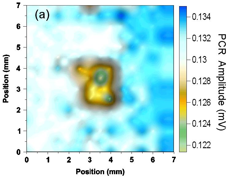
4 L ( ω) ( λ, λ ) (, ω) P F N z (4) with dz ( + + ) λ1 ( λ λ ) [ ( λ) ] ( λ) [ ( λ) 1, 2 = λ ] F R R b (5) 2 R η W ( λ) C( λ) d λ The PCR signal is the integration of Eq. (4) over the image of the detector on the sample and thus is directly proportional to the depth integral of the carrier density in the sample. Consequently, the relative lateral concentration of any defects that affect the carrier density, either by enhancing recombination or altering diffusion coefficients, can be determined by scanning the surface of the wafer with the PCR probe. In addition, frequency scan techniques can be used with the appropriate carrier diffusion model to obtain quantitative values for the four transport parameters (Rodriguez et al. (2000)). This quantitative technique can be combined with surface scans to provide quantitative imaging of the semiconductor sample. PCR Imaging NDT of Electronic Defects in Si Wafers Instrumentation and Signal Characteristics The experimental implementation of laser infrared photo-carrier radiometry is similar to the typical PTR set-up for semiconductors (Mandelis (1998); Rodriguez et al. (2000), with the crucial difference being that the spectral window of the IR detector and optical filter, and the modulation frequency response of the preamplifier stage, must be tailored through spectral bandwidth matching to a combination of carrier recombination emissions and effective spectral filtering of the Planck-mediated thermal infrared emission band. Conventional PTR utilizes photoconductive liquid-nitrogen-cooled HgCdTe (MCT) detectors with spectral bandwidth in the 2-12 µm range. This includes the thermal infrared range, 7-12 µm, and only part of the electronic emission spectrum at shorter wavelengths. From experiments with several IR detectors and bandpass optical filters we concluded that emissive infrared radiation from electronic CW recombination in Si is centered mainly in the spectral region below 3 µm. The IR detector was a switchable-gain InGaAs element (ThorLabs model PDA400), 1-mm in diameter, with spectral response in the nm range, peak response at 1550 nm and frequency bandwidth from dc to 10 MHz. The preamplifier was incorporated into the detector housing, a design which delivered optimal signalto-noise ratio expressed as a NEP figure of x10-12 W/ Hz. The detector was outfitted with a specialty long-pass optical filter from Spectrogon featuring very steep cut-on (5% at 1010 nm, 78% at 1060 nm, and transmission range nm). The cut-on quality of the filter is crucial in PCR as it must block any pump radiation leakage from reaching the highly sensitive detector. Short-wavelength filtering of optical density 5 or 6 is usually required. The samples were placed on an aluminum backing which acted as a support, heater, and signal amplifier by redirecting the forward emitted IR photons back toward the detector (Mandelis et al. (2003)), Fig.1. The incident Ar-ion laser beam size was 1.06 mm and the power was mw. The detector was proven extremely effective in cutting off all thermal infrared radiation: Preliminary measurements using non-electronic materials (metals, thin foils and rubber) showed no responses whatsoever. PCR Imaging of Deep Sub-Surface Electronic Defects Figure 2 shows line scans with the excitation laser beam scanning the front (polished) surface of a 20 Ωcm p-type Si wafer and the IR detector on the same side. Based on the backing R er
5 results, for maximum signal strength the sample was resting on a mirror. At all three selected modulation frequencies, the PCR amplitude decreases when the laser beam scans over the defect region, consistent with the expected CW density decrease as the back-surface defect efficiently traps carriers and removes them from further diffusion and potential radiative recombination. The PCR phase scan remains essentially constant at 10 Hz, Fig. 2b, as the diffusion-wave centroid is solely determined by the ac carrier-wave diffusion length (van Roosbroeck and Shockley (1954); Mandelis et al. (2003)) L D ( ω ) = ac 1 + (6) * τ i ωτ where τ is the lifetime and D* is the ambipolar carrier diffusion coefficient. This particular wafer was measured to have τ 1 ms and D* 12 cm 2 /s, which yields an L ac (10 Hz) 1.1 mm. Therefore, the CW centroid lies well beyond the thickness of the wafer (~ 630 µm) and no phase shift can be observed. At the intermediate frequency of 1360 Hz, L ac 373 µm, well within the bulk of the wafer. In this case, a phase lead appears within the defective region. This occurs because the CW spatial distribution across the body of the wafer in the defective region is weighed more heavily toward the front surface on account of the heavy depletion occurring at, and near, the back surface. As a result, the CW centroid is shifted toward the front surface, manifested by a phase lead. Finally, at 100 khz, L ac 44 µm. Nevertheless, Fig. 2a shows that there is still PCR amplitude contrast at that frequency, accompanied by a small phase lead, Fig. 2b. Figure 3 shows images of the back-surface defect obtained through front-surface inspection at the optimum contrast frequency of 1360 Hz. Figure 4 shows the same scan at 100 khz. At this frequency the PCR image clearly shows the highest spatial resolution of the back-surface defect possible. The PCR phase, Fig. 4b, shows details of the central defect as well as the Figure 2. Line scans over an p-si wafer region with backsurface mechanical damage. (a) PCR amplitude; (b) PCR phase. The wafer is resting on a mirror support. Laser power: 24 mw. radially diverging defect structures at the base of the central defect, like a "zoomed in" version of the 1360 Hz image, Fig. 3b. Both PCR images clearly reveal internal sub-structure of the central defect, which was invisible at 1360 Hz. In a manner reminiscent of conventional propagating wavefields, image resolution increases with decreasing carrier wavelength, L ac. Under front-surface inspection and precise depth profilometric control by virtue of the PCR modulation-frequencyadjustable carrier-wave diffusion length, Eq. (6), Figs. 3 and 4 show for the first time that with today's high-quality, long-lifetime industrial Si wafers, one can observe full images of sharp carrier-wave density contrast due to underlying defects very deep
6 PCR Amplitude (mv) PCR Phase (degrees) (a) f = 10 Hz f = 1360 Hz f = 100 khz Position (mm) (b) f = 10 Hz f = 1360 Hz f = 100 khz Position (mm) inside the bulk of a Si wafer. Specifically, high frequency PCR imaging reveals so far unknown very long-range effects of carrier interactions with deep sub-surface defect structures and the detrimental ability of such structures to decrease the overall free photoexcited-carrier density far away from the defect sites at or near the front surface where device fabrication takes place. This phenomenon may be important toward device fabrication improvement through careful selection of substrate wafers with regard to deep bulk growth and manufacturing defects which were heretofore not associated with device performance. Further PCR imaging experiments with shorter lifetime Si wafers have shown that it may be beneficial to use lower quality starting substrates in order to avoid the full effects of deep sub-surface defects on the electronic quality of the upper (device-level) surface.

7
 PCR amplitude; (b) PCR phase.")

8 Figure 3. Scanning imaging of back-surface defect in the p-si wafer using front-surface inspection. Laser beam radius: 518 µm. Frequency: 1360 Hz. (a) PCR amplitude; (b) PCR phase. Figure 4. Scanning imaging of back-surface defect in the p-si wafer using front-surface inspection. Laser beam radius: 518 µm. Frequency: 100 khz. (a) PCR amplitude; (b) PCR phase. deep sub-surface defects which may result in unpredictably variable performance and electronic quality of the upper (device-level) surface. Quantitative PCR Measurements Of Electronic Transport Properties The PCR image contrast of Figs. 3 and 4 can, in principle, be quantified by use of the CW term in Eq. (4), appropriately modified to accommodate the defective region: P( ω) F( λ, λ ) N( z, ω) dz N ( z, ω) (7) L L 0 0 d dz where P(ω) is the difference in signal between the intact and defective regions. This is a complex quantity, so it can be separated out into amplitude and phase components. The apparent
9 simplicity of this expression is due to the fact that the sub-surface defects considered here are on the back surface of the wafer and their presence mostly impacts the value of the back-surface recombination velocity S 2 (Mandelis (2001)), while the bulk transport parameters and the terms comprising the prefactor F(λ 1,λ 2 ), remain essentially unaltered for a thin damage layer in an otherwise homogeneous semiconductor. If these conditions are not fulfilled, then a more complete expression of the carrier recombination related emissions must be used to quantify PCR contrast due to distributed sub-surface electronic defect structures. 1 (a) PCR Amplitude (mv) PCR Phase (degrees) E Frequency (khz) Front outside Front inside Back outside Back inside Front outside Front inside Back outside Back inside (b) Frequency (khz) Figure 5: Front- and back-surface PCR frequency scans inside and outside a defect area of a p-si wafer on aluminum backing. Best fits to the data of Eq. (4) were made using the carrierdensity-wave field N(z,ω) expression Eq. (9.106) in Mandelis (2001). Detector: InGaAs; beam size: 1.4 mm; Ar-ion laser power: 20 mw. (a) Amplitudes and (b) phases. Best fit parameters: Front intact region: τ = 1 ms; D* = 12 cm 2 /s, S 1 = 10 cm/s, S 2 = 210 cm/s. Front inside the defect: τ = 1 ms; D* = 14.9 cm 2 /s, S 1 = 25 cm/s, S 2 = 300 cm/s. Back intact region: τ = 1 ms; D* = 12 cm 2 /s, S 1 = 10 cm/s, S 2 = 200 cm/s. Back inside the defect: τ = 1 ms; D* = 5 cm 2 /s, S 1 = 450 cm/s, S 2 = 130 cm/s. The mild mechanical defect on the back surface of the p-type Si wafer that generated the images of Figs. 3 and 4 proved to be too severe for our sensitive InGaAs photodetector: upon scanning the affected surface the PCR signal vanished within the region of the defect, apparently due to the highly efficient trapping of the photogenerated free carriers by the high density of nearsurface electronic defect states. Therefore, a different region of the same wafer was chosen to create a visually undetectable defect by simply touching the back surface of the wafer with paper. Then PCR frequency scans were performed on both sides of the material, outside and inside the defect region, Fig. 5. The inherent instrumental transfer function was removed by introducing an indirect normalization method based on the fact that in the high frequency regime both HgCdTe and InGaAs detectors monitor the same electronic processes (Mandelis et al. (2003)). All curves shown here were normalized by the same transfer function obtained by this method. The PCR theoretical model involved carrier-wave IR emissions using diffusion-wave field expressions (Mandelis (2001), Chap. 9.12), with adjustable electronic transport coefficients (Rodriguez et al. (2000); Ikari et al. (1999)). The effect of the back-surface defect was modeled as a change in the recombination velocity S 2 (front-surface probing) only. When the wafer was turned over, the
10 definitions of S 1 and S 2 were reversed. Regarding the D* values, those outside the defect remained constant for both sides of the wafer, however, the D* value from the back inside the defect region was relatively low. The high sensitivity of the InGaAs detector to the electronic state of the inspected surface is probably responsible for this discrepancy, as the theoretical phase fit is poor at high frequencies (> 1 khz) within that region, an indication of near-surface depth inhomogeneity of transport properties. Conclusions Laser infrared photo-carrier radiometry (PCR) has been introduced. This technique is a photonic method based on carrier diffusion-wave diagnostics. Based on the theoretical foundations and the first few experimental case studies using industrial-quality Si wafers, there are excellent prospects for PCR as an in-situ quality control NDT technology in semiconductor processing. Its local monitoring nature surpasses the currently available techniques for non-destructive, non-contact monitoring and imaging of deep electronic defects in Si wafers, for measuring free-carrier transport properties without the need for auxiliary electric circuit fabrication and electrode application. PCR can become a valuable NDT technology as it can monitor local values of carrier mobilities and other transport properties at several intermediate stages of device fabrication. A noteworthy feature of high frequency PCR imaging is that it has revealed for the first time a very long-range effect of carrier interactions with deep sub-surface defect structures and the detrimental ability of such structures to decrease the overall free photoexcited-carrier density in locations far away from the defect sites at or near the front surface where device fabrication takes place. Therefore, PCR may become an important tool toward device fabrication improvement through careful selection of substrate wafers with regard to deep bulk growth and manufacturing defects which were heretofore not associated with device performance. Acknowledgments I wish to acknowledge the support of the Natural Sciences and Engineering Research Council of Canada (NSERC) for a Discovery Grant, and of Materials and Manufacturing Ontario (MMO) for a Collaborative Contract which made this research possible. References Christofides, C., Nestoros, M. & Othonos, A in Semiconductors and Electronic Materials. Progress Photoacoustic and Photothermal Phenomena Vol. IV (A. Mandelis and P. Hess, eds., SPIE, Bellingham, WA, 2000), Chap. 4. Ikari, T., Salnick, A. & Mandelis, A Journal of Applied Physics. 85: Kirchhoff, G Abhandlungen über Emission und Absorption. (M. Planck, Ed., Verlag von Wilhelm Engelmann, Leipsig), Mandelis, A Solid-State Electron. 42(1). Mandelis, A Diffusion-Wave Fields: Mathematical Methods and Green Functions, Springer-Verlag, NY, Chap. 9. Mandelis, A., Batista, J. & Shaughnessy, D Phys. Rev. B 67: Rodriguez, M.E., Mandelis, A., Pan, G., Nicolaides, L., Garcia, J.A. & Riopel, Y J. Electrochem. Soc. 147: 687. Rosencwaig, A in Photoacoustic and Thermal-Wave Phenomena in Semiconductors. (A. Mandelis, Ed., North-Holland, New York), Chap. 5. Salnick, A., Jean, C. & Mandelis, A. 1997a. Solid-State Electron. 41: 591.
11 Smith, R.A Semiconductors, 2nd Ed. (Cambridge Univ. Press, Cambridge), 118. van Roosbroeck, W. & Shockley, W Phys. Rev. 94: Wagner, R.E. & Mandelis, A Semicond. Sci. Technol. 11: 300.
Received 16 November 2001; received in revised form 19 October The review of this paper was arranged by Prof. C. Hunt
 Solid-State Electronics 49 (2005) 769 773 www.elsevier.com/locate/sse Ion implantation dose high-resolution monitoring in Si wafers using laser infrared photothermal radiometry with lock-in common-mode-rejection
Lecture 18: Photodetectors
 Lecture 18: Photodetectors Contents 1 Introduction 1 2 Photodetector principle 2 3 Photoconductor 4 4 Photodiodes 6 4.1 Heterojunction photodiode.................... 8 4.2 Metal-semiconductor photodiode................
Luminous Equivalent of Radiation
 Intensity vs λ Luminous Equivalent of Radiation When the spectral power (p(λ) for GaP-ZnO diode has a peak at 0.69µm) is combined with the eye-sensitivity curve a peak response at 0.65µm is obtained with
A. Mandelis, R. Bleiss. To cite this version: HAL Id: jpa
 Highly-resolved separation of carrier and thermal wave contributions to photothermal signals from Cr-doped silicon using rate-window infrared radiometry A. Mandelis, R. Bleiss To cite this version: A.
OPTOELECTRONIC and PHOTOVOLTAIC DEVICES
 OPTOELECTRONIC and PHOTOVOLTAIC DEVICES Outline 1. Introduction to the (semiconductor) physics: energy bands, charge carriers, semiconductors, p-n junction, materials, etc. 2. Light emitting diodes Light
ECE 340 Lecture 29 : LEDs and Lasers Class Outline:
 ECE 340 Lecture 29 : LEDs and Lasers Class Outline: Light Emitting Diodes Lasers Semiconductor Lasers Things you should know when you leave Key Questions What is an LED and how does it work? How does a
Key Questions. What is an LED and how does it work? How does a laser work? How does a semiconductor laser work? ECE 340 Lecture 29 : LEDs and Lasers
 Things you should know when you leave Key Questions ECE 340 Lecture 29 : LEDs and Class Outline: What is an LED and how does it How does a laser How does a semiconductor laser How do light emitting diodes
Physics of Waveguide Photodetectors with Integrated Amplification
 Physics of Waveguide Photodetectors with Integrated Amplification J. Piprek, D. Lasaosa, D. Pasquariello, and J. E. Bowers Electrical and Computer Engineering Department University of California, Santa
Semiconductor Lasers Semiconductors were originally pumped by lasers or e-beams First diode types developed in 1962: Create a pn junction in
 Semiconductor Lasers Semiconductors were originally pumped by lasers or e-beams First diode types developed in 1962: Create a pn junction in semiconductor material Pumped now with high current density
LAB V. LIGHT EMITTING DIODES
 LAB V. LIGHT EMITTING DIODES 1. OBJECTIVE In this lab you are to measure I-V characteristics of Infrared (IR), Red and Blue light emitting diodes (LEDs). The emission intensity as a function of the diode
Vertical External Cavity Surface Emitting Laser
 Chapter 4 Optical-pumped Vertical External Cavity Surface Emitting Laser The booming laser techniques named VECSEL combine the flexibility of semiconductor band structure and advantages of solid-state
Optodevice Data Book ODE I. Rev.9 Mar Opnext Japan, Inc.
 Optodevice Data Book ODE-408-001I Rev.9 Mar. 2003 Opnext Japan, Inc. Section 1 Operating Principles 1.1 Operating Principles of Laser Diodes (LDs) and Infrared Emitting Diodes (IREDs) 1.1.1 Emitting Principles
Cavity QED with quantum dots in semiconductor microcavities
 Cavity QED with quantum dots in semiconductor microcavities M. T. Rakher*, S. Strauf, Y. Choi, N.G. Stolz, K.J. Hennessey, H. Kim, A. Badolato, L.A. Coldren, E.L. Hu, P.M. Petroff, D. Bouwmeester University
LAB V. LIGHT EMITTING DIODES
 LAB V. LIGHT EMITTING DIODES 1. OBJECTIVE In this lab you will measure the I-V characteristics of Infrared (IR), Red and Blue light emitting diodes (LEDs). Using a photodetector, the emission intensity
Semiconductor Lasers Semiconductors were originally pumped by lasers or e-beams First diode types developed in 1962: Create a pn junction in
 Semiconductor Lasers Semiconductors were originally pumped by lasers or e-beams First diode types developed in 1962: Create a pn junction in semiconductor material Pumped now with high current density
Semiconductor Optical Communication Components and Devices Lecture 18: Introduction to Diode Lasers - I
 Semiconductor Optical Communication Components and Devices Lecture 18: Introduction to Diode Lasers - I Prof. Utpal Das Professor, Department of lectrical ngineering, Laser Technology Program, Indian Institute
Optical Amplifiers. Continued. Photonic Network By Dr. M H Zaidi
 Optical Amplifiers Continued EDFA Multi Stage Designs 1st Active Stage Co-pumped 2nd Active Stage Counter-pumped Input Signal Er 3+ Doped Fiber Er 3+ Doped Fiber Output Signal Optical Isolator Optical
Photomixer as a self-oscillating mixer
 Photomixer as a self-oscillating mixer Shuji Matsuura The Institute of Space and Astronautical Sciences, 3-1-1 Yoshinodai, Sagamihara, Kanagawa 9-8510, Japan. e-mail:matsuura@ir.isas.ac.jp Abstract Photomixing
LEDs, Photodetectors and Solar Cells
 LEDs, Photodetectors and Solar Cells Chapter 7 (Parker) ELEC 424 John Peeples Why the Interest in Photons? Answer: Momentum and Radiation High electrical current density destroys minute polysilicon and
Solar Cell Parameters and Equivalent Circuit
 9 Solar Cell Parameters and Equivalent Circuit 9.1 External solar cell parameters The main parameters that are used to characterise the performance of solar cells are the peak power P max, the short-circuit
Chapter 3 OPTICAL SOURCES AND DETECTORS
 Chapter 3 OPTICAL SOURCES AND DETECTORS 3. Optical sources and Detectors 3.1 Introduction: The success of light wave communications and optical fiber sensors is due to the result of two technological breakthroughs.
Instruction manual and data sheet ipca h
 1/15 instruction manual ipca-21-05-1000-800-h Instruction manual and data sheet ipca-21-05-1000-800-h Broad area interdigital photoconductive THz antenna with microlens array and hyperhemispherical silicon
Nd:YSO resonator array Transmission spectrum (a. u.) Supplementary Figure 1. An array of nano-beam resonators fabricated in Nd:YSO.
 Supplementary Figure 1. An array of nano-beam resonators fabricated in Nd:YSO.") a Nd:YSO resonator array µm Transmission spectrum (a. u.) b 4 F3/2-4I9/2 25 2 5 5 875 88 λ(nm) 885 Supplementary Figure. An array of nano-beam resonators fabricated in Nd:YSO. (a) Scanning electron microscope
a Nd:YSO resonator array µm Transmission spectrum (a. u.) b 4 F3/2-4I9/2 25 2 5 5 875 88 λ(nm) 885 Supplementary Figure. An array of nano-beam resonators fabricated in Nd:YSO. (a) Scanning electron microscope
Quantum-Well Semiconductor Saturable Absorber Mirror
 Chapter 3 Quantum-Well Semiconductor Saturable Absorber Mirror The shallow modulation depth of quantum-dot saturable absorber is unfavorable to increasing pulse energy and peak power of Q-switched laser.
Photodiode: LECTURE-5
 LECTURE-5 Photodiode: Photodiode consists of an intrinsic semiconductor sandwiched between two heavily doped p-type and n-type semiconductors as shown in Fig. 3.2.2. Sufficient reverse voltage is applied
1 Semiconductor-Photon Interaction
 1 SEMICONDUCTOR-PHOTON INTERACTION 1 1 Semiconductor-Photon Interaction Absorption: photo-detectors, solar cells, radiation sensors. Radiative transitions: light emitting diodes, displays. Stimulated emission:
Applications of Steady-state Multichannel Spectroscopy in the Visible and NIR Spectral Region
 Feature Article JY Division I nformation Optical Spectroscopy Applications of Steady-state Multichannel Spectroscopy in the Visible and NIR Spectral Region Raymond Pini, Salvatore Atzeni Abstract Multichannel
InP-based Waveguide Photodetector with Integrated Photon Multiplication
 InP-based Waveguide Photodetector with Integrated Photon Multiplication D.Pasquariello,J.Piprek,D.Lasaosa,andJ.E.Bowers Electrical and Computer Engineering Department University of California, Santa Barbara,
Lecture 4 INTEGRATED PHOTONICS
 Lecture 4 INTEGRATED PHOTONICS What is photonics? Photonic applications use the photon in the same way that electronic applications use the electron. Devices that run on light have a number of advantages
Department of Electrical Engineering and Computer Science, Massachusetts Institute of Technology, 77. Table of Contents 1
 Efficient single photon detection from 500 nm to 5 μm wavelength: Supporting Information F. Marsili 1, F. Bellei 1, F. Najafi 1, A. E. Dane 1, E. A. Dauler 2, R. J. Molnar 2, K. K. Berggren 1* 1 Department
Application Instruction 002. Superluminescent Light Emitting Diodes: Device Fundamentals and Reliability
 I. Introduction II. III. IV. SLED Fundamentals SLED Temperature Performance SLED and Optical Feedback V. Operation Stability, Reliability and Life VI. Summary InPhenix, Inc., 25 N. Mines Road, Livermore,
Quantum Condensed Matter Physics Lecture 16
 Quantum Condensed Matter Physics Lecture 16 David Ritchie QCMP Lent/Easter 2018 http://www.sp.phy.cam.ac.uk/drp2/home 16.1 Quantum Condensed Matter Physics 1. Classical and Semi-classical models for electrons
Lecture 6 Fiber Optical Communication Lecture 6, Slide 1
 Lecture 6 Optical transmitters Photon processes in light matter interaction Lasers Lasing conditions The rate equations CW operation Modulation response Noise Light emitting diodes (LED) Power Modulation
Review of Semiconductor Physics
 Review of Semiconductor Physics k B 1.38 u 10 23 JK -1 a) Energy level diagrams showing the excitation of an electron from the valence band to the conduction band. The resultant free electron can freely
Thermal management and thermal properties of high-brightness diode lasers
 Thermal management and thermal properties of high-brightness diode lasers Jens W. Tomm Max-Born-Institut für Nichtlineare Optik und Kurzzeitspektroskopie Berlin Max-Born-Str. 2 A, D-12489 Berlin, Germany
Examination Optoelectronic Communication Technology. April 11, Name: Student ID number: OCT1 1: OCT 2: OCT 3: OCT 4: Total: Grade:
 Examination Optoelectronic Communication Technology April, 26 Name: Student ID number: OCT : OCT 2: OCT 3: OCT 4: Total: Grade: Declaration of Consent I hereby agree to have my exam results published on
BMC s heritage deformable mirror technology that uses hysteresis free electrostatic
 Optical Modulator Technical Whitepaper MEMS Optical Modulator Technology Overview The BMC MEMS Optical Modulator, shown in Figure 1, was designed for use in free space optical communication systems. The
A Thesis submitted in partial fulfillment of the requirements for the degree of Master of Science at George Mason University
 Auger Suppression in MWIR InSb Photodiode for Ambient Temperature Operation A Thesis submitted in partial fulfillment of the requirements for the degree of Master of Science at George Mason University
LEP Optical pumping
 Related topics Spontaeous emission, induced emission, mean lifetime of a metastable state, relaxation, inversion, diode laser. Principle and task The visible light of a semiconductor diode laser is used
Ultra-sensitive, room-temperature THz detector using nonlinear parametric upconversion
 15 th Coherent Laser Radar Conference Ultra-sensitive, room-temperature THz detector using nonlinear parametric upconversion M. Jalal Khan Jerry C. Chen Z-L Liau Sumanth Kaushik Ph: 781-981-4169 Ph: 781-981-3728
Chap14. Photodiode Detectors
 Chap14. Photodiode Detectors Mohammad Ali Mansouri-Birjandi mansouri@ece.usb.ac.ir mamansouri@yahoo.com Faculty of Electrical and Computer Engineering University of Sistan and Baluchestan (USB) Design
Micro-sensors - what happens when you make "classical" devices "small": MEMS devices and integrated bolometric IR detectors
 Micro-sensors - what happens when you make "classical" devices "small": MEMS devices and integrated bolometric IR detectors Dean P. Neikirk 1 MURI bio-ir sensors kick-off 6/16/98 Where are the targets
Tunable wideband infrared detector array for global space awareness
 Tunable wideband infrared detector array for global space awareness Jonathan R. Andrews 1, Sergio R. Restaino 1, Scott W. Teare 2, Sanjay Krishna 3, Mike Lenz 3, J.S. Brown 3, S.J. Lee 3, Christopher C.
Angela Piegari ENEA, Optical Coatings Laboratory, Roma, Italy
 Optical Filters for Space Instrumentation Angela Piegari ENEA, Optical Coatings Laboratory, Roma, Italy Trieste, 18 February 2015 Optical Filters Optical Filters are commonly used in Space instruments
Basic concepts. Optical Sources (b) Optical Sources (a) Requirements for light sources (b) Requirements for light sources (a)
 Optical Sources (a) Requirements for light sources (b) Requirements for light sources (a)") Optical Sources (a) Optical Sources (b) The main light sources used with fibre optic systems are: Light-emitting diodes (LEDs) Semiconductor lasers (diode lasers) Fibre laser and other compact solid-state
Optical Sources (a) Optical Sources (b) The main light sources used with fibre optic systems are: Light-emitting diodes (LEDs) Semiconductor lasers (diode lasers) Fibre laser and other compact solid-state
Introduction Fundamentals of laser Types of lasers Semiconductor lasers
 ECE 5368 Introduction Fundamentals of laser Types of lasers Semiconductor lasers Introduction Fundamentals of laser Types of lasers Semiconductor lasers How many types of lasers? Many many depending on
Coherent Receivers Principles Downconversion
 Coherent Receivers Principles Downconversion Heterodyne receivers mix signals of different frequency; if two such signals are added together, they beat against each other. The resulting signal contains
Design and Analysis of Resonant Leaky-mode Broadband Reflectors
 846 PIERS Proceedings, Cambridge, USA, July 6, 8 Design and Analysis of Resonant Leaky-mode Broadband Reflectors M. Shokooh-Saremi and R. Magnusson Department of Electrical and Computer Engineering, University
Dynamics of Charge Carriers in Silicon Nanowire Photoconductors Revealed by Photo Hall. Effect Measurements. (Supporting Information)
") Dynamics of Charge Carriers in Silicon Nanowire Photoconductors Revealed by Photo Hall Effect Measurements (Supporting Information) Kaixiang Chen 1, Xiaolong Zhao 2, Abdelmadjid Mesli 3, Yongning He 2*
Dynamics of Charge Carriers in Silicon Nanowire Photoconductors Revealed by Photo Hall Effect Measurements (Supporting Information) Kaixiang Chen 1, Xiaolong Zhao 2, Abdelmadjid Mesli 3, Yongning He 2*
Low Thermal Resistance Flip-Chip Bonding of 850nm 2-D VCSEL Arrays Capable of 10 Gbit/s/ch Operation
 Low Thermal Resistance Flip-Chip Bonding of 85nm -D VCSEL Arrays Capable of 1 Gbit/s/ch Operation Hendrik Roscher In 3, our well established technology of flip-chip mounted -D 85 nm backside-emitting VCSEL
Design and Simulation of N-Substrate Reverse Type Ingaasp/Inp Avalanche Photodiode
 International Refereed Journal of Engineering and Science (IRJES) ISSN (Online) 2319-183X, (Print) 2319-1821 Volume 2, Issue 8 (August 2013), PP.34-39 Design and Simulation of N-Substrate Reverse Type
Single-photon excitation of morphology dependent resonance
 Single-photon excitation of morphology dependent resonance 3.1 Introduction The examination of morphology dependent resonance (MDR) has been of considerable importance to many fields in optical science.
Detectors for Optical Communications
 Optical Communications: Circuits, Systems and Devices Chapter 3: Optical Devices for Optical Communications lecturer: Dr. Ali Fotowat Ahmady Sep 2012 Sharif University of Technology 1 Photo All detectors
RECENTLY, using near-field scanning optical
 1 2 1 2 Theoretical and Experimental Study of Near-Field Beam Properties of High Power Laser Diodes W. D. Herzog, G. Ulu, B. B. Goldberg, and G. H. Vander Rhodes, M. S. Ünlü L. Brovelli, C. Harder Abstract
Lecture 19 Optical Characterization 1
 Lecture 19 Optical Characterization 1 1/60 Announcements Homework 5/6: Is online now. Due Wednesday May 30th at 10:00am. I will return it the following Wednesday (6 th June). Homework 6/6: Will be online
High Speed pin Photodetector with Ultra-Wide Spectral Responses
 High Speed pin Photodetector with Ultra-Wide Spectral Responses C. Tam, C-J Chiang, M. Cao, M. Chen, M. Wong, A. Vazquez, J. Poon, K. Aihara, A. Chen, J. Frei, C. D. Johns, Ibrahim Kimukin, Achyut K. Dutta
By emitter degradation analysis of high power diode laser bars. Outline Part I
 By emitter degradation analysis of high power diode laser bars Eric Larkins and Jens W. Tomm Outline Part I I. 1. Introduction I. 2. Experimental Techniques I. 3. Case Study 1: Strain Threshold for Increased
A Coherent White Paper May 15, 2018
 OPSL Advantages White Paper #3 Low Noise - No Mode Noise 1. Wavelength flexibility 2. Invariant beam properties 3. No mode noise ( green noise ) 4. Superior reliability - huge installed base The optically
10/14/2009. Semiconductor basics pn junction Solar cell operation Design of silicon solar cell
 PHOTOVOLTAICS Fundamentals PV FUNDAMENTALS Semiconductor basics pn junction Solar cell operation Design of silicon solar cell SEMICONDUCTOR BASICS Allowed energy bands Valence and conduction band Fermi
Problem 4 Consider a GaAs p-n + junction LED with the following parameters at 300 K: Electron diusion coecient, D n = 25 cm 2 =s Hole diusion coecient
 Prof. Jasprit Singh Fall 2001 EECS 320 Homework 7 This homework is due on November 8. Problem 1 An optical power density of 1W/cm 2 is incident on a GaAs sample. The photon energy is 2.0 ev and there is
SUPPLEMENTARY INFORMATION
 SUPPLEMENTARY INFORMATION Supplementary Information Real-space imaging of transient carrier dynamics by nanoscale pump-probe microscopy Yasuhiko Terada, Shoji Yoshida, Osamu Takeuchi, and Hidemi Shigekawa*
Doppler-Free Spetroscopy of Rubidium
 Doppler-Free Spetroscopy of Rubidium Pranjal Vachaspati, Sabrina Pasterski MIT Department of Physics (Dated: April 17, 2013) We present a technique for spectroscopy of rubidium that eliminates doppler
Lecture 14: Photodiodes
 Lecture 14: Photodiodes Background concepts p-n photodiodes photoconductive/photovoltaic modes p-i-n photodiodes responsivity and bandwidth Reading: Senior 8.1-8.8.3 Keiser Chapter 6 1 Electron-hole photogeneration
OPTI510R: Photonics. Khanh Kieu College of Optical Sciences, University of Arizona Meinel building R.626
 OPTI510R: Photonics Khanh Kieu College of Optical Sciences, University of Arizona kkieu@optics.arizona.edu Meinel building R.626 Photodetectors Introduction Most important characteristics Photodetector
Scintillation Counters
 PHY311/312 Detectors for Nuclear and Particle Physics Dr. C.N. Booth Scintillation Counters Unlike many other particle detectors, which exploit the ionisation produced by the passage of a charged particle,
What is the highest efficiency Solar Cell?
 What is the highest efficiency Solar Cell? GT CRC Roof-Mounted PV System Largest single PV structure at the time of it s construction for the 1996 Olympic games Produced more than 1 billion watt hrs. of
Lasers PH 645/ OSE 645/ EE 613 Summer 2010 Section 1: T/Th 2:45-4:45 PM Engineering Building 240
 Lasers PH 645/ OSE 645/ EE 613 Summer 2010 Section 1: T/Th 2:45-4:45 PM Engineering Building 240 John D. Williams, Ph.D. Department of Electrical and Computer Engineering 406 Optics Building - UAHuntsville,
CONTENTS. 2.2 Schrodinger's Wave Equation 31. PART I Semiconductor Material Properties. 2.3 Applications of Schrodinger's Wave Equation 34
 CONTENTS Preface x Prologue Semiconductors and the Integrated Circuit xvii PART I Semiconductor Material Properties CHAPTER 1 The Crystal Structure of Solids 1 1.0 Preview 1 1.1 Semiconductor Materials
UNIT-III SOURCES AND DETECTORS. According to the shape of the band gap as a function of the momentum, semiconductors are classified as
 UNIT-III SOURCES AND DETECTORS DIRECT AND INDIRECT BAND GAP SEMICONDUCTORS: According to the shape of the band gap as a function of the momentum, semiconductors are classified as 1. Direct band gap semiconductors
Title detector with operating temperature.
 Title Radiation measurements by a detector with operating temperature cryogen Kanno, Ikuo; Yoshihara, Fumiki; Nou Author(s) Osamu; Murase, Yasuhiro; Nakamura, Masaki Citation REVIEW OF SCIENTIFIC INSTRUMENTS
Key Questions ECE 340 Lecture 28 : Photodiodes
 Things you should know when you leave Key Questions ECE 340 Lecture 28 : Photodiodes Class Outline: How do the I-V characteristics change with illumination? How do solar cells operate? How do photodiodes
SUPPLEMENTARY INFORMATION
 SUPPLEMENTARY INFORMATION doi:10.1038/nature10864 1. Supplementary Methods The three QW samples on which data are reported in the Letter (15 nm) 19 and supplementary materials (18 and 22 nm) 23 were grown
Supplementary Figure 1 Reflective and refractive behaviors of light with normal
 Supplementary Figures Supplementary Figure 1 Reflective and refractive behaviors of light with normal incidence in a three layer system. E 1 and E r are the complex amplitudes of the incident wave and
Mercury Cadmium Telluride Detectors
 Mercury Cadmium Telluride Detectors ISO 9001 Certified J15 Mercury Cadmium Telluride Detectors (2 to 26 µm) General HgCdTe is a ternary semiconductor compound which exhibits a wavelength cutoff proportional
Fiberoptic Communication Systems By Dr. M H Zaidi. Optical Amplifiers
 Optical Amplifiers Optical Amplifiers Optical signal propagating in fiber suffers attenuation Optical power level of a signal must be periodically conditioned Optical amplifiers are a key component in
Optical Fiber Communication Lecture 11 Detectors
 Optical Fiber Communication Lecture 11 Detectors Warriors of the Net Detector Technologies MSM (Metal Semiconductor Metal) PIN Layer Structure Semiinsulating GaAs Contact InGaAsP p 5x10 18 Absorption InGaAs
GaAs polytype quantum dots
 GaAs polytype quantum dots Vilgailė Dagytė, Andreas Jönsson and Andrea Troian December 17, 2014 1 Introduction An issue that has haunted nanowire growth since it s infancy is the difficulty of growing
Absorption: in an OF, the loss of Optical power, resulting from conversion of that power into heat.
 Absorption: in an OF, the loss of Optical power, resulting from conversion of that power into heat. Scattering: The changes in direction of light confined within an OF, occurring due to imperfection in
Spectrally Selective Photocapacitance Modulation in Plasmonic Nanochannels for Infrared Imaging
 Supporting Information Spectrally Selective Photocapacitance Modulation in Plasmonic Nanochannels for Infrared Imaging Ya-Lun Ho, Li-Chung Huang, and Jean-Jacques Delaunay* Department of Mechanical Engineering,
EQE Measurements in Mid-Infrared Superlattice Structures
 University of Iowa Honors Theses University of Iowa Honors Program Spring 2018 EQE Measurements in Mid-Infrared Superlattice Structures Andrew Muellerleile Follow this and additional works at: http://ir.uiowa.edu/honors_theses
Light Sources, Modulation, Transmitters and Receivers
 Optical Fibres and Telecommunications Light Sources, Modulation, Transmitters and Receivers Introduction Previous section looked at Fibres. How is light generated in the first place? How is light modulated?
Bistability in Bipolar Cascade VCSELs
 Bistability in Bipolar Cascade VCSELs Thomas Knödl Measurement results on the formation of bistability loops in the light versus current and current versus voltage characteristics of two-stage bipolar
Optical Receivers Theory and Operation
 Optical Receivers Theory and Operation Photo Detectors Optical receivers convert optical signal (light) to electrical signal (current/voltage) Hence referred O/E Converter Photodetector is the fundamental
Grant Soehnel* and Anthony Tanbakuchi
 Simulation and experimental characterization of the point spread function, pixel saturation, and blooming of a mercury cadmium telluride focal plane array Grant Soehnel* and Anthony Tanbakuchi Sandia National
Figure 1. Schematic diagram of a Fabry-Perot laser.
 Figure 1. Schematic diagram of a Fabry-Perot laser. Figure 1. Shows the structure of a typical edge-emitting laser. The dimensions of the active region are 200 m m in length, 2-10 m m lateral width and
Infrared Detection Module for Free Space Optics
 PIERS ONLINE, VOL. 6, NO. 4, 2010 380 Infrared Detection Module for Free Space Optics Marcin Ratajczyk 1, Ryszard Paliwoda 1, Maciej Rzeczkowski 1, Waldemar Gawron 2, Jaros law Pawluczyk 1, and Józef Piotrowski
Design and operation influences regarding rise and fall time of a photoconductive microwave switch
 Loughborough University Institutional Repository Design and operation influences regarding rise and fall time of a photoconductive microwave switch This item was submitted to Loughborough University's
Theory and Applications of Frequency Domain Laser Ultrasonics
 1st International Symposium on Laser Ultrasonics: Science, Technology and Applications July 16-18 2008, Montreal, Canada Theory and Applications of Frequency Domain Laser Ultrasonics Todd W. MURRAY 1,
Components of Optical Instruments. Chapter 7_III UV, Visible and IR Instruments
 Components of Optical Instruments Chapter 7_III UV, Visible and IR Instruments 1 Grating Monochromators Principle of operation: Diffraction Diffraction sources: grooves on a reflecting surface Fabrication:
First Observation of Stimulated Coherent Transition Radiation
 SLAC 95 6913 June 1995 First Observation of Stimulated Coherent Transition Radiation Hung-chi Lihn, Pamela Kung, Chitrlada Settakorn, and Helmut Wiedemann Applied Physics Department and Stanford Linear
FIBER OPTICS. Prof. R.K. Shevgaonkar. Department of Electrical Engineering. Indian Institute of Technology, Bombay. Lecture: 18.
 FIBER OPTICS Prof. R.K. Shevgaonkar Department of Electrical Engineering Indian Institute of Technology, Bombay Lecture: 18 Optical Sources- Introduction to LASER Diodes Fiber Optics, Prof. R.K. Shevgaonkar,
Lecture 9 External Modulators and Detectors
 Optical Fibres and Telecommunications Lecture 9 External Modulators and Detectors Introduction Where are we? A look at some real laser diodes. External modulators Mach-Zender Electro-absorption modulators
Notes on Optical Amplifiers
 Notes on Optical Amplifiers Optical amplifiers typically use energy transitions such as those in atomic media or electron/hole recombination in semiconductors. In optical amplifiers that use semiconductor
SECOND HARMONIC GENERATION AND Q-SWITCHING
 SECOND HARMONIC GENERATION AND Q-SWITCHING INTRODUCTION In this experiment, the following learning subjects will be worked out: 1) Characteristics of a semiconductor diode laser. 2) Optical pumping on
Today s Outline - January 25, C. Segre (IIT) PHYS Spring 2018 January 25, / 26
 PHYS Spring 2018 January 25, / 26") Today s Outline - January 25, 2018 C. Segre (IIT) PHYS 570 - Spring 2018 January 25, 2018 1 / 26 Today s Outline - January 25, 2018 HW #2 C. Segre (IIT) PHYS 570 - Spring 2018 January 25, 2018 1 / 26 Today
Today s Outline - January 25, 2018 C. Segre (IIT) PHYS 570 - Spring 2018 January 25, 2018 1 / 26 Today s Outline - January 25, 2018 HW #2 C. Segre (IIT) PHYS 570 - Spring 2018 January 25, 2018 1 / 26 Today
PERFORMANCE OF PHOTODIGM S DBR SEMICONDUCTOR LASERS FOR PICOSECOND AND NANOSECOND PULSING APPLICATIONS
 PERFORMANCE OF PHOTODIGM S DBR SEMICONDUCTOR LASERS FOR PICOSECOND AND NANOSECOND PULSING APPLICATIONS By Jason O Daniel, Ph.D. TABLE OF CONTENTS 1. Introduction...1 2. Pulse Measurements for Pulse Widths
EFFECT OF SURFACE COATINGS ON GENERATION OF LASER BASED ULTRASOUND
 EFFECT OF SURFACE COATINGS ON GENERATION OF LASER BASED ULTRASOUND V.V. Shah, K. Balasubramaniam and J.P. Singh+ Department of Aerospace Engineering and Mechanics +Diagnostic Instrumentation and Analysis
Optical Gain Experiment Manual
 Optical Gain Experiment Manual Table of Contents Purpose 1 Scope 1 1. Background Theory 1 1.1 Absorption, Spontaneous Emission and Stimulated Emission... 2 1.2 Direct and Indirect Semiconductors... 3 1.3
Dr. Rüdiger Paschotta RP Photonics Consulting GmbH. Competence Area: Fiber Devices
 Dr. Rüdiger Paschotta RP Photonics Consulting GmbH Competence Area: Fiber Devices Topics in this Area Fiber lasers, including exotic types Fiber amplifiers, including telecom-type devices and high power
arxiv:physics/ v1 [physics.optics] 28 Sep 2005
![arxiv:physics/ v1 [physics.optics] 28 Sep 2005](/thumbs/91/105523130.jpg "arxiv:physics/ v1 [physics.optics] 28 Sep 2005") Near-field enhancement and imaging in double cylindrical polariton-resonant structures: Enlarging perfect lens Pekka Alitalo, Stanislav Maslovski, and Sergei Tretyakov arxiv:physics/0509232v1 [physics.optics]
Near-field enhancement and imaging in double cylindrical polariton-resonant structures: Enlarging perfect lens Pekka Alitalo, Stanislav Maslovski, and Sergei Tretyakov arxiv:physics/0509232v1 [physics.optics]