EE 414: Lab 4 Frequency Synthesizer-based Local Oscillator
|
|
|
- Michael Garrison
- 6 years ago
- Views:
Transcription
1 Abstract EE 414: Lab 4 Frequency Synthesizer-based Local Oscillator Saket Vora Andy Chen Siddharth Panwar This lab explores the design, construction, and testing of a frequency synthesizer based local oscillator (LO) to be used in the superhetereodyne receiver block. Previous laboratory investigations looked at antennas, filters, and low noise amplifiers. Two voltage controlled oscillators and their respective PLL boards (referred to as Alpha and Beta) were constructed and tested. Locking was obtained at all five frequencies of interest (900MHz to 1GHz in 25MHz increments) though Alpha featured excellent high frequency performance, whereas Beta succeeded in maintaining sufficient output power at all frequencies while featuring insufficient spur suppression at only the 1GHz frequency. In both cases however, the frequency synthesizer LO was unable to perform at a single DC level shift voltage (used to match the output of the loop filter with the tuning range of the VCO). Phase noise measurements and spectrum analyzer results are shown. An addendum to this lab is found at the end with full measurement results for a repaired Beta VCO & PLL. Introduction Local oscillators are an important component in wireless communication systems because they allow for the proper demodulation of a received signal. This lab explores the design, construction, and testing of a frequency synthesizer based local oscillator (LO) to be used in the superhetereodyne receiver block. Previous laboratory investigations looked at antennas, filters, and low noise amplifiers. The following specifications were expected to be satisfied: Frequency Range 900 MHz f 1000 MHz In 25MHz intervals Output Power Spur Suppression > 0dBm -30 dbc 5 to 7 dbm preferred Table 1 - Specifications for VCO/PLL Phase Margin 45 degrees Consisting of a phase locked loop and a voltage controlled oscillator, this LO can be programmed to generate a range of frequencies. Figure 2 shows the simplified block diagram for this topology used in this lab. Reference Frequency N Phase Detector Loop Filter VCO f out M Figure 2 - Block model of the frequency synthesizer-based LO This is a feedback control system in which the variable of interest in phase. This topology is known as a phased lock loop (PLL) and is used to generate frequencies that are multiples of a given reference frequency. A quartz crystal resonator is used to provide a stable 25 MHz reference frequency. The phase detector block compares an incoming signal s phase to that of the reference and generates an output signal that is a function of the phase difference. This signal is conditioned by a loop filter before reaching the voltage controlled oscillator (VCO), which is an oscillator that produces an output at some frequency that is a function of the input voltage. The divider blocks, N and M, allow for the synthesis of different frequencies. They are related by: 1
2 fref fout M fout N M N f ref By adjusting the M divide factor, different output frequencies can be obtained. The various blocks in Figure 1 will be described in greater detail in the sections below. A note on terminology: though the architecture is known as a PLL, this lab features a partitioning between the VCO and the rest of the PLL. The former will still be referred to as the VCO, but the latter is often denoted as the PLL board. Also, two separate VCOs and PLL boards (Alpha and Beta) were constructed and tested and show different characteristics. Unfortunately, due to mechanical failure with Beta, there are incomplete results in terms of phase noise. Frequency Synthesizer & PLL Board This component of the lab involves the Motorola MC12181 integrated circuit which includes the phase detector, dividers, and charge pump for the PLL as well as the loop filter. Printed circuit boards were used to mount the IC, loop filter, DIP switch, crystal oscillator, and later the level shifter. A more detailed block diagram of the PLL is shown below in Figure MHz Crystal 8 Phase Detector Charge Pump Loop Filter Level Shifter VCO 8 M (25 to 40) DIP Switch Figure 3 - Detailed block diagram of PLL. The dashed area indicates which components are contained inside the MC12181 chip. Prescalers of 8 are included in the reference frequency path and in the return path. A 25MHz quartz crystal oscillator loaded with two 15 pf capacitors and a 50k ohm feedback biasing resistor provides the reference frequency. The crystal was checked for third overtone operation by measuring it on a spectrum analyzer and this was confirmed not to be the case. The MC12181 supports 4-bit programming of the feedback path divider allows the user to select the desired frequency multiplier and ranges from 25 to 40. Using the formula M 8 (25to 40) fout fref 25 MHz N 8, this provides a range of 625MHz to 1000MHz. Integer M values of 36 to 40 correspond to the five frequencies of interest, 900MHz to 1000MHz in 25MHz intervals. A brief overview of the theory of operation: the phase detector compares the phase of the feedback signal to the reference signal. If the feedback signal is deemed slow, as in the VCO needs to increase its output frequency to provide the desired frequency as set by the DIP switch, a charge pump deposits charge onto a capacitor, thus increasing the control voltage to the VCO. If the feedback signal is too fast, an ideally equal and opposite charge pump removes charge, lowering the control voltage to the VCO. The loop filter contains this capacitor performs further signal conditioning. A resistor provides a loop-stabilizing zero and is included in series with the integrating capacitor. Injected noise into the control voltage line and asymmetries in the charge pump or phase detector can be periodic in nature and thus produce sideband spurs. The loop filter should also smooth out the characteristic sawtooth pattern response of the phase 2

3 detector. Higher order filters are naturally more complex and greater care is needed to ensure stability. It has been found that while a fourth-order loop filter is optimum, a third-order filter is sufficient and is more straightforward to design. A loop filter design tool by National Semiconductor (PLL_LpFltr) was used to design a third-order filter, shown in Figure 4. The tool requests a charge pump current I c, VCO gain constant K VCO, loop bandwidth, divider, phase margin, and desired spur attenuation. I C = 2.2mA from the datasheet, and since the VCO was currently in development, a gain constant of 20 to 25 MHz/V (22 MHz/V actual) was estimated for K VCO. Though a 45 degree phase margin was specified, we expected degradation in the phase margin in the process of realizing the circuit, so the loop filter was over-designed to 56 degree phase margin, and for the same reason the attenuation was set at 40 db. The loop bandwidth was another parameter was iterated. The loop bandwidth plays a critical role in the transmitter block, and has to do with how fast the loop acts. A bandwidth of 100 khz was initially chosen but then increased to 200 khz after it was suspected that the loop filter was not reacting fast enough to acquire and maintain a lock. to VCO from charge pump R 0 C 0 C A R x C x Figure 4-3rd Order Loop Filter The values obtained by the loop filter and the actual values used are shown along with the frequency response of the filter in the table and figure below. Component Designed Actual Value Value Used R o 93.6pF 94pF C o 3.1nF 3.0nF C A 2.68k 2.67k R X 54.1k 54.9k C X 9.36pF 9.4pF Figure 5 - Component values for Loop Filter and Frequency Response Another important issue that had to be addressed was the loading of the VCO due to the PLL board. The output signal of the VCO is tapped to create the feedback system. This tapped signal is tied to the F in pin on the MC12181 and is fed into the prescaler, frequency multiplier, and finally to the phase detector. This pin has a parasitic capacitance of a couple picofarads and is ac-coupled to the feedback signal through a large DC blocking capacitor. A VNA was used to characterize the F in pin and a Smith chart is shown in Figure 6. 3
 side of the Smith chart. There is a zero-reactance line crossing at 986MHz and 1041MHz.")


4 Figure 6 - S 11 of the Fin pin on MC12181 Frequency Synthesizer Of particular interest is the region on the horizontal terminator on the left (open) side of the Smith chart. There is a zero-reactance line crossing at 986MHz and 1041MHz. One idea suggested by Siddharth Seth was to create a through path using two BNC connectors connected with a 50 ohm transmission line and then capacitively tapping that line to the F in pin. The f out of VCO would connect to one BNC and the line to the spectrum analyzer would be connected to the other. This method was attempted on both boards, with slight changes in the layout. Both constructed boards are shown below in Figure 7 and Figure 8. From VCO Out 1mm 3mm Fin Pin 3mm 9mm Open Figure 7 Alpha s PLL Board 4


5 Fin Pin From VCO Out 4mm 3mm 3mm 7mm 3mm 15mm Open Figure 8 Beta s PLL Board Alpha s board was the first one to try the transmission like idea and poor construction technique made it difficult to create a clean tap. Beta s board was newer and thus shows a better tap. Alpha s board uses 1nF capacitor as the DC block, Beta s board uses two 1nF for greater physical geometry matching. Through testing, it was deemed that the method was actually degrading performance and if the other BNC connector was left open, the PLL locked and maintained sufficient output power. Presumably, the F in does not need large amounts of signal power to function, and so maximum power transfer is not required. Voltage Controlled Oscillator A Colpitts oscillator topology, a positive feedback system that is capacitively tapped, was chosen for the VCO and is shown in Figure 9. L R 2 C 1 R 1 C b R e Figure 9 - Initial Topology for Colpitts Voltage Controlled Oscillator Voltage control is provided by using a varactor that adjusts an LC tank s capacitance and thus frequency of oscillation. This control voltage is supplied by the Motorola MC12181 chip (described below) and is constrained to a 0.5V to 4.5V range. We began based on the assumption that this would directly act as the control voltage for the varactor diode, which can be tuned between 8pF to 18pF in that voltage range. 5
6 The effective capacitance of the tank is given by the series combination of C 1 and C 2 and is thus given by CC C C. For very large values of C 2 the capacitance then approaches C 1 and this is what we want. In order to be able to control the tank capacitance we need C 1 to dominate the total tank capacitance and hence C 2 was chosen to be 22 pf because under all circumstances it will be greater than C 1 and since we are targeting relatively large frequencies it is prudent to not make any the capacitance in the tank unnecessarily large. Making C 2 extremely large would prove detrimental because this capacitor acts as a feedback capacitor and the principle on which the oscillator works is that this capacitor is charged when the transistor is on and the moment the capacitor voltage rises high enough then the base-emitter junction is no longer forward biased, and the transistor switches off. As the charge from the capacitor diminishes and the base voltage rises above the emitter voltage the junction is forward-biased again and the transistor begins operation. If the capacitor is so large that it does not lose charge quickly then in the next cycle when the voltage at the base again rises it would not be sufficient to forward bias the baseemitter junction. The most challenging aspect of building the oscillator was to obtain the right inductance for the tank circuit. We now compute an estimate of the inductance that we need to have oscillation from 900MHz to 1GHz. Assuming there is about 4 pf of parasitic capacitance at the emitter of the transistor being contributed by C that gets added in parallel of C 2, the total capacitance of the tank varies from (8 (22+4)) pf = 6.11pF to (18 (22+4)) pf= 10.63pF when the control voltage goes from 0.5 V to 4.5 V. The average of these values is around 8pF and that is where we want our center frequency to be tuned. In this lab we are trying to achieve a tuning range from 900 MHz to 1 GHz so the center frequency is 950 MHz. The corresponding inductor value is given by L 2 1 C, where C tot is 8pF and is 5.96 Grad/s. The inductance therefore needs to be around 3.5nH. If we make the naïve assumption that we are not picking up any parasitic inductance from the components leads and solder etc. then we can compute the length of the transmission line that we need to provide this much inductance from the following equation that is derived from the impedance transformation equation for a load much smaller than the characteristic impedance of the transmission line, i.e., Z L << Z 0. This conditioned is obtained by shorting one of the ends of the transmission line to ground. Z( z) Z j tan( l) or L 0 Zo j tan( l) 2 f 0 tot, where Z 0 is 50 ohm, f 0 is the center frequency, and is the wavelength of a 950 MHz wave on the FR4 board and is equal to 300 mm x = 163 mm. The length of the line, l, that we get from the above computation is approximately 9 mm. While performing the above calculations we realize that the impedances required are small enough that tan( l) l, implying a linear relationship between impedance and length of the line, so it is reasonable to state that we get 1 nh from every 3 mm of 50 ohm copper strip on FR4. It must be mentioned that choosing a wider line which has characteristic impedance less than 50 ohm allows us to use a longer strip of line but that results in a drop in the Q factor of the inductance that we are trying to obtain and it does not result in a inductor as good as we desire. The output of the oscillator, V tank, is given by V tank = 2 I BIAS R tank (1-n), where R tank is the tank load and (1-n) is the multiplicative factor that has to be included because that comes from the large-signal input resistance of the transistor that is reflected from the capacitive impedance transformer and adds to the load of the tank. Here n is given by C 1 /(C 1 +C 2 ). 6
7 The requirement for oscillations to occur is that the loop transmission magnitude should be greater than unity and another way of expressing that is that g m > 1/R tank [n-n 2 ]. Combined with the equation of V tank mentioned above, this equation can help us choose the right bias current, I BIAS, that would ensure that oscillations occur for the chosen I BIAS and we meet the specified output power between 0-7dBm or 1-5 mw. This implies 1mW 2 V 2 out 50 5mW or 0.316V < V out < V. The challenge then is to tap the transmission line such that resistance looking into the tap point is 50 ohm so that maximum power can be transferred and then compute the corresponding load seen by the tank, R tank, through the inductive impedance transformer. This can be computed using the equation for tapped impedance transformer formed by the inductive transmission line we have at the collector of the transistor under the assumption that Q of this transformer is much greater than 1. We get the following equation for resistance looking into the output port, R tap, of the oscillator R L ( ) where R out is the output resistance of the transistor seen by the impedance 1 2 tap R out L1 L2 transformer at the collector node of the transistor and L 1 and L 2 are the inductance values above and below the tap point. In this case R out is given by r o (1+g m R e ) and for g m R e >>1 it reduces to r o g m R e, where r o =V A /I c and g m =I c /V T. V A is the early voltage and V T is the thermal voltage. Therefore V I V 50 A C A Rout Re Re Re 2000 I C VT VT.025 R e If we can choose an appropriate tap point and hence L 1 and L 2, we can transform the R out above to R tap = 50 ohm to get maximum power transfer. And due to reciprocity of the network the 50 ohm load, R tap, will be transformed to R out at the collector node (the node with V tank potential) and R tank becomes R out R out =R out /2 (it own output resistance and the one transformed from the load combined in parallel with each other). However this entire procedure hinges on the aforementioned assumption of Q >> 1 or L/R tap >> 1 or L >> 50ohm or L >> 8-9 nh. This is certainly not the case and thus we cannot follow this procedure to compute the right tap point, hence R tank followed by I BIAS and V tank to meet our power requirement and oscillation requirement. Thus we simply follow the procedure suggested in the text. We first choose a bias voltage of -8 V to so that we have some margin later to increase it if there is a need to increase the bias current. We then assume a current we wish to bias our oscillator at and that we choose based on the efficiency that we expect from our oscillator. Given that we need a maximum of 7 dbm output power which translates to 5 mw and we expect about 10% efficiency then our static power dissipation should be around 50 mw. So for a 8V supply the bias current is 6.25 ma. Now to bias the circuit at this current we assume that we drop 2V across the emitter resistance, R e, which comes out to be 3/6.25mA = 320 ohm. We then assume about 1/10 th of the bias current flows through the biasing transistors R 1 and R 2 (with the assumption that base current is zero) The voltage drop across the two resistors is 8 V and therefore the sum of two resistors, (R 1 +R 2 ), is 8V/.625 ma = ohm. Since we dropped two volts across the emitter resistance the emitter voltage is given by -6 V and if 0.75 V drop occurs from the base to emitter then the base voltage is V. So using the voltage divider equation we can compute R 1 /(R 1 +R 2 )=5.25/8. We then get R 1 =8400 ohm and R 2 =4400 ohm. We use 1 F bypass capacitor at the base of the transistor and, as suggested in the text, use 1 k resistance between the control voltage and the cathode of the varactor. Few attempts with the copper strip acting as the inductor reveal that the parasitic inductance is too high and the parasitics are enough to provide the ~3 nh we are looking for. So taking the advice of the TA we simply used the collector lead of the transistor to act as our inductance. Despite doing that we found it difficult to reach 1 GHz range. So to push the frequency up we reduced the value of C 2 to 5 pf from previously chosen 22 pf. When even this did not work we completely removed this capacitor and used 7


8 the inherent capacitance of the transistor as our C 2. We see that C is almost 10 pf from the equation for diffusion capacitance C b V T I c T, peak and that is ample for our requirements. We must also mention that extreme care was taken in the physical layout of the oscillator, as seen in Figure 10. No wire or transmission line was used to connect two components in the circuit and they were all placed right next to each other and connected by means of solder. R e was later changed from 320 ohm to 150 ohm to roughly double the current to improve output power. The final constructed VCO by Panwar is shown in Figure 10. Ground 2.5mm 18mm OUT 3mm Vctrl 6mm Vcc Distance to tap: 1.5mm Ground Figure 10 - Beta s VCO The above design prescription reflects the choices made for Beta s VCO. Chen built a separate VCO utilizing the same key principles removal of C 2 capacitor due to presence of parasitics and using the collector lead to provide the tank inductance. Next, the VCOs was characterized for their output power and frequency range versus control voltage sweep, known as tuning curves. A VCO meter was used to provide a sweeping control voltage and to measure the output of the VCO. The tuning curve for Beta s VCO is shown in Figure 11. This was measured with the standalone VCO. 8
9 Figure 11 - Tuning Curve for Beta s VCO, Unloaded As the graph shows, the tuning curve is increasing with an uneven slope and a voltage range of 6.4V to 8.9V is needed to obtain the 900MHz to 1GHz desired frequency range, which is an 40MHz/V gain constant using straight-line approximation. Note that this is higher than the 0.5V to 4.5V the VCO was desired for, which corresponds to a smaller varactor capacitance in the 3pF to 6pF range, as seen from the varactor datasheet. As the output of the VCO is the T-connector that creates the feedback tap and also a thru-path for the output to a spectrum analyzer or VCO meter. When loaded with this structure, the tuning curve changes to that seen in Figure 12, with a straight-line approximation gain constant of ~20 MHz/V. Figure 12 - Tuning Curve for Beta s VCO, Loaded with PLL board 9


10 Finally, a look at the output power vs control voltage in Figure 13 for Beta s unloaded VCO shows sufficient output power across a wide tuning range. Figure 13 - Output Power vs Control Voltage, Beta s VCO, Unloaded The characterization performed above was repeated for Alpha s VCO, whose physical construction is shown in Figure 14. It too places high importance in reducing parasitics by short path lengths. The collector here is tapped directly at the start, with the lead going just 2mm before contacting the ground plane. Chen used a thru-hole in order to position the 2SC3302 transistor in a more optimal orientation. An expansive ground plane surrounds the VCO structure. Vcc Vctrl 2mm 6mm Distance to tap: ~0mm 3mm OUT Ground Figure 14 - Alpha s VCO with Entire Structure and VCO Close-Up Tuning curves were measured for Alpha s board for the unloaded and loaded cases, shown in Figure 15 and Figure 16, respectively. 10
11 Figure 15 - Tuning Curve for Alpha s VCO, Unloaded Figure 16 - Tuning Curve for Alpha s VCO, Loaded with PLL Board Here the effect is again seen of voltage control spreading and corresponding reduction in gain constant when the VCO is loaded. The gain constant goes from 42MHz/V unloaded to 23.4MHz when loaded down. This further validates the assumption used for the PLL loop filter of gain constants between 20 and 25 MHz. Finally, the output power vs control voltage for Alpha s unloaded VCO is shown in Figure
12 Figure 17 - Output Power vs Control Voltage for Alpha s VCO, Unloaded Unlike Beta s VCO, this VCO shows lower output power and one that falls below the minimum of 0 dbm within the tuning range. Adjustments were made to the tapping, but the power could not be raised without sacrificing functionality. Level Shifter A significant challenge in building the oscillator was obtaining a inductance as small as 3 nh for the tank circuit while accommodating the innumerable inductive parasitics that were being contributed from almost all the elements that were placed on the board. After several attempts it was evident that to have a resonance frequency as high as 1 GHz the capacitance in the tank had to be reduced for which not only did we have to completely get rid of C 2 but also reduce the capacitance of the varactor by providing a control voltage that was much higher than PLL was generating. The datasheet of the MC12181 IC states that its output will be 0.5V to 4.5V for a 5V charge pump supply voltage, but our oscillator was needed a higher control voltage that ranged from ~6V to ~13.5V depending on loading to tune from 900MHz to 1GHz. Additionally, not only are the DC values higher than what the MC12181 can provide, the actual tuning range is not necessarily 4V. Furthermore, losses in the remaining loop filter stages could cause other changes in the control voltage that the VCO sees. To provide the DC shift and to modify the tuning range, a summing operational amplifier circuit was used as shown in Figure
13 V LS R shift R s from loop filter R gain to VCO R f R a Figure 18 - Summing Amplifier Level Shifter A dual op-amp IC (model NTE928M) was used for the single-supply op-amp block. The V LS, or level shifter supply voltage, was used to both power the op-amp and provide the DC source that is scaled through the R shift resistor. The following equations can be used to find the output voltage: R V V V f out LS O, LF Rshift R R f gain, with V O,LF being the output voltage from the level shifter. The R S and R a Rf Rf Rf Rf resistors are used to satisfy stability rules: 1 R R R R. s a gain shift Rf = Rs was arbitrarily chosen as 5k ohm and the remaining resistor values were designed for VLS = 13V. Rshift = 12.1k to obtain a DC shift of 5.38V, while the voltage range from the loop filter was increased by ~1.5x by setting Rgain = 3.3k ohm. This resulted in a Ra = 2.61k ohm. Note that these values are for the Beta. The design methodology remained the same for the Alpha. The values for Alpha were for a V LS = 20V, with R shift = 5k ohm and R a = 4.03k ohm. As a final check, the Alpha and Beta VCOs were tested with a tuning voltage being fed into the level shifter. If the level shifter was properly functioning, the 900MHz to 1000MHz range should be comfortably attainable with an input of 0.5V to 4.5V. Figure 19 and Figure 20 show the tuning curves under this setup for the Alpha and Beta PLLs, respectively. 13
14 Figure 19 - Tuning Curve for Alpha s VCO with Level Shifter, Open Loop Figure 20 - Tuning Curve for Beta s VCO, with Level Shifter, Open Loop Alpha needs a control voltage from loop filter between 1.31V and 4.38V while Beta requires 0.92V to 3.92V, both ranges that should be comfortably supplied by the MC The gain constants, using straight-line approximation again, are 32.5MH/V and 33.5 MH/V, respectively. Closing the Loop The PLL entered closed-loop operation when the output of the loop filter was connected to the input to the level shifter. The output was observed on the spectrum analyzer. There were numerous obstacles in the journey towards obtaining lock at the desired frequencies. 14

15 Figure 21 - Photo of the Closed Loop Setup Figure 21 shows a picture of how the PLL board (on the left) connects with the VCO board (right side) through a T-connector. An early problem encountered was that the DIP switches that set the desired frequency seemed to have no effect on the output. V LS (and thus the DC shift) was varied and the frequency output would shift, but the shape of the signal did not convey that a lock had occurred. An oscilloscope was used to probe various points with mixed results. We soon realized that the MC12181 chip was not consuming current so it was replaced. The typical testing procedure involved setting the DIP switch to the desired frequency then adjusting V LS such that a lock would occur. This was visually confirmed when the spectrum analyzer signal would become very distinct and the presence of side spurs could be clearly seen. The next desired frequency would be set and V LS further changed to obtain lock. Proper PLL operation would have a single V LS for all frequencies, so that all the user has to do is adjust the DIP switches to generate the desired frequencies. Despite many long hours analyzing the behavior of the level shift circuit, loading phenomenon, and replacing ICs, we were unable to achieve this. It was clear by documenting the output voltages from the loop filter and the level shifter for each of the frequencies that the act of closing the loop changed the tuning range of the VCO and thus made the previously designed level shifter no longer optimal. In order to mitigate this effect, a unity gain buffer between the loop filter and the level shifter was tried, utilizing the 2 nd op-amp in the NTE928M IC. However, it is believed that this taxed the stability of the loop and would often cause hashing in the spectrum analyzer output, such as in Figure
 extended this range. In other iterations, a lock could be obtained but it would be a loose one, with lots of shifting.")

16 Figure 22 - Examples of unity gain buffer causing hashing in spectrum Some iterations saw that high or low frequencies could not be locked; the oscillator would only tune to a certain point. Adjusting the V LS (ie, DC shift of the level shifter) extended this range. In other iterations, a lock could be obtained but it would be a loose one, with lots of shifting. Reflowing the solder joints usually rectified this problem, but it also motivated the change to a higher loop bandwidth, with us believing (erroneously or not) that the PLL would reduce this seek time by speeding up the loop. Despite the inability to operate from a single, constant V LS, both Alpha and Beta PLLs were able to achieve a lock at all five frequencies of interest, albeit with differing characteristics. The measurements for both Alpha and Beta PLLs are discussed below. Results The Alpha PLL features excellent reference spur (f ref ) attenuation at all five frequencies of interest, approaching -60dBc in the case of the 1000MHz lock. However, while the output power at 975MHz and 1000MHz is quite good at 4.2dBm and 6.5dBm, respectively, the output power falls below 0dBm for the 925MHz and 900MHz frequencies. Table 23 shows the full measurements results, including phase noise measured at 100kHz and 1MHz offset from the carrier. These measurements were taken at a MC12181 supply voltage of 4.95V and a VCO supply voltage of -7.44V. Frequency (MHz) Output Power (dbm) Alpha (Alpha s VCO & Alpha s board) Results f ref Spur Phase Noise Attenuation 100 khz Offset (dbc) (dbc) Phase Noise 1 MHz Offset (dbc) V LS Supply (V) Table 23 - Results for Alpha 16


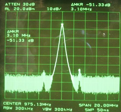
17 Figure 24 - Alpha's 1 GHz Lock, Output Power & Spur Attenuation Figure 24 shows the spectrum analyzer for Alpha s 1000MHz lock. The left image shows the output power measured at the peak and the right image shows the difference between the power at the carrier and an offset of ~3.10 MHz, which corresponds to the reference spur. Figure 25 shows the phase noise measured with the VCO meter for the 1000Mhz lock, averaged over 8 time periods. Spectrum analyzer images and phase noise measurements for the remaining four frequencies of interest can be found in Appendix A. Figure 25 - Alpha's Phase Noise, 100 khz offset from 1 GHz carrier Finally, a summary of the minimum, nominal, and maximum gain constants for Alpha s VCO is shown in Table 26. Condition Minimum (MHz/V) Nominal (MHz/V) Maximum (MHz/V) Unloaded Loaded Loaded w/ Level Shift Table 26 - Gain constant summary for Alpha 17

, because the orientation and contacting of the board caused changes to")
18 The Beta PLL provided more even performance across the frequency range. The measurements for Beta used a MC12181 supply voltage of 4.88V and a VCO supply voltage of V. The output power remained sufficient, ranging from 2.7dBm to 3.5dBm. The -30dBc spur attenuation specification was satisfies for all frequencies except 1000MHz, where the spurs were at -21.3dBc. Adjustments to the bias voltage and the V Ls did not reduce these spurs. Indeed, it is suspected that injected noise due to a layout issue at the root cause (or at least a contributor of several db), because the orientation and contacting of the board caused changes to occur. The Beta PLL took the brunt of the numerous iterating and debugging. After the spectrum analyzer images were taken, the phase noise measurements were about to begin when the voltage supply BNC connector to the Beta VCO broke off and took with it the resistors and capacitors used in the VCO. Time constraints did not permit a quick fix, so phase noise measurements for the Beta VCO are not included in this lab report. An addendum will be filed later that contains this data. Frequency (MHz) Output Power (dbm) Beta (Beta s VCO & Board 2) Results Phase Phase Noise Noise 100 khz 1 MHz Offset Offset f ref Spur Attenuation (dbc) V LS Supply (V) na na na na na na na na na na Table 27 - Results for Beta V OLF (V) V OLS (V) Figure 28 - Beta's 1 GHz Lock, Output Power & Spur Attenuation As Figure 28 shows, the spur attenuation for Beta at 1000MHz is significantly worse than the Alpha board or any other frequency locked by Beta (full results shown in Appendix B). The left image also shows the characteristic shape on the spectrum analyzer while spanning a wide bandwidth (200MHz) when lock has been achieved. Table 29 summarizes the minimum, nominal, and maximum gain constants for different conditions for the VCO. Condition Minimum (MHz/V) Nominal (MHz/V) Maximum (MHz/V) Unloaded Loaded ~ ~36 Loaded w/ Level Shift ~ ~36 Table 29 - Gain constant summary for Beta 18
19 Conclusion This laboratory investigation lived up to its reputation as the most challenging assignment. The PLL is not a trivial block to understand and implement, and the voltage controlled oscillator is a whole task itself. Collaboration was key in constructing the VCO, particularly the result that parasitic and stray capacitances are sufficient to warrant the removal of C 2 all together in the Colpitts topology. For the PLL board, the most difficult element to implement was the level shifter. The nature of loading various components (the VCO, the loop filter, etc) resulted in an optimization design problem with a goal that was always moving. Ultimately however, we were able to achieve lock at all frequencies of interest and met nearly all the specifications for each frequency too. We would have liked to have done so with a constant V LS for indeed, this is what significant time was spent in trying to achieve. 19


20 Appendix A Alpha Full Results for 900 MHz to 975 MHz Frequency Range Output Power & Spur Attenuation 900 MHz: 925 MHz: Figure 30 - Alpha's 900 MHz Lock, Output Power & Spur Attenuation Figure 31 - Alpha's 925 MHz Lock, Output Power & Spur Attenuation 20


21 950 MHz: Figure 32 - Alpha's 950 MHz Lock, Output Power & Spur Attenuation 975 MHz: Figure 33 - Alpha's 975 MHz Lock, Output Power & Spur Attenuation 21
22 Phase Noise 900 MHz: Figure 34 - Alpha's 900 MHz Lock, Phase Noise 925 MHz: Figure 35 - Alpha's 925 MHz Lock, Phase Noise 22
23 950 MHz: Figure 36 - Alpha's 950 MHz Lock, Phase Noise 975 MHz: Figure 37 - Alpha's 975 MHz Lock, Phase Noise 23


24 Appendix B Loading Characterization of the VCO Saket Vora Andy Chen Siddharth Panwar The output of the VCO first goes through a BNC connector, then a T-connector to which the BNC-input to the F in is connected and the cable to the spectrum analyzer or the noise meter. This total loading structure was characterized on the VNA for both Chen and Beta s board, shown below: Figure 38 - S 11 of VCO s Load using Alpha s VCO & Board in Smith Chart & Log Magnitude Figure 39 - S 11 Looking into VCO's Load, Beta s VCO & Board, Smith Chart & Log Magnitude Board & Frequency Smith Chart Log Magnitude Chen 900 MHz j db 1000 MHz j db Panwar 900 MHz j db 1000 MHz j db Figure 40 - Loading Seen by the VCOs 24
25 Introduction Lab 4 VCO/PLL Addendum for Beta s Measurements As stated in the original report, Beta s VCO broke during testing and due to time constraints, a full suite of measurements could not not taken. Our group succeeded in repairing the VCO and have performance a new set of measurements of the Beta VCO and PLL. The performance of the newly fixed VCO actually improved performance. Output power was higher at all frequencies of interest and the one frequency that failed to meet the -30dBc reference spur attenuation specification by ~9dB came closer to meeting it at -27.3dBc. Results The Beta PLL provided more even performance across the frequency range. The measurements for Beta used a MC12181 supply voltage of 5V and a VCO supply voltage of V. The output power remained sufficient, ranging from 4.9dBm to 7.33dBm. The -30dBc spur attenuation specification was satisfies for all frequencies except 1000MHz, where the spurs were at -27.3dBc. Adjustments to the bias voltage and the V Ls did not reduce these spurs. Indeed, it is suspected that injected noise due to a layout issue at the root cause (or at least a contributor of several db), because the orientation and contacting of the board caused changes to occur. The Beta PLL took the brunt of the numerous iterating and debugging. After the VCO broke, as mentioned in the original report, it was repaired and re-tested. The following measurements should supercede those found in the original report, as they represent the current performance of Beta. Frequency (MHz) Output Power (dbm) Beta (Beta s VCO & Board 2) Results Phase f ref Spur Noise Attenuation 100 khz (dbc) Offset Phase Noise 1 MHz Offset V LS Supply (V) Figure 41 - Results for Beta Spectrum analyzer plots were printed from the instrument and can be found attached to the printed report. A phase noise measurement for Beta is shown in Figure
26 Figure 42 - Phase Noise measurement for Beta at 1GHz Because it was noticed that the output power characteristics had changed with the repaired Beta VCO, the tuning curves were measured again. Figure 43 shows a very linear tuning curve for the unloaded VCO, with a range of 5.93V to 8.4V corresponding to 900MHz and 1GHz, respectively. Figure 43 - Tuning Curve for Unloaded Beta VCO 26
27 Figure 44 - Tuning Curve for Beta VCO Loaded with PLL Board When the VCO is loaded by the PLL board as shown in Figure 44, the control voltage required shifts upward to a range of 7.62V to 10.74V. The voltage range changes from 2.5V unloaded to 3.1V loaded. The tuning curve s shape is nonetheless quite linear, with a small change above 1GHz. Figure 45 - Tuning Curve for Beta VCO with Loaded PLL Board Plus Level Shifted Input Finally, when the level shifter is added and the VCO meter outputs a voltage range from 0.35V to 4.6V, a range in which the output range from the MC12181 IC resides. Figure 45 shows that while the tuning curve remains quite linear, the IC s output has to range from 1.42V to 3.5V, which should be a comfortable range to provide. 27
28 Table 29 summarizes the minimum, nominal, and maximum gain constants for different conditions for the VCO. It can be seen that as the VCO is tested in settings more like the one it is finally intended for, the gain constant reduces. Condition Minimum (MHz/V) Nominal (MHz/V) Maximum (MHz/V) Unloaded Loaded Loaded w/ Level Shift Table 46 - Gain constant summary for Beta 28
29 Appendix C Beta Phase Noise Results for 900 MHz to 975 MHz Frequency Range 900 MHz: Saket Vora Andy Chen Siddharth Panwar 925 MHz: Figure 47 Beta's Phase Noise at 900MHz Carrier Figure 48 - Beta's Phase Noise at 925MHz Carrier 29
30 950 MHz: Figure 49 - Beta's Phase Noise at 950MHz Carrier 975 MHz: Figure 50 - Beta's Phase Noise at 975MHz Carrier 30
PART MAX2605EUT-T MAX2606EUT-T MAX2607EUT-T MAX2608EUT-T MAX2609EUT-T TOP VIEW IND GND. Maxim Integrated Products 1
 19-1673; Rev 0a; 4/02 EVALUATION KIT MANUAL AVAILABLE 45MHz to 650MHz, Integrated IF General Description The are compact, high-performance intermediate-frequency (IF) voltage-controlled oscillators (VCOs)
EVALUATION KIT AVAILABLE 10MHz to 1050MHz Integrated RF Oscillator with Buffered Outputs. Typical Operating Circuit. 10nH 1000pF MAX2620 BIAS SUPPLY
 19-1248; Rev 1; 5/98 EVALUATION KIT AVAILABLE 10MHz to 1050MHz Integrated General Description The combines a low-noise oscillator with two output buffers in a low-cost, plastic surface-mount, ultra-small
Lab 4. Crystal Oscillator
 Lab 4. Crystal Oscillator Modeling the Piezo Electric Quartz Crystal Most oscillators employed for RF and microwave applications use a resonator to set the frequency of oscillation. It is desirable to
Keywords: ISM, RF, transmitter, short-range, RFIC, switching power amplifier, ETSI
 Maxim > Design Support > Technical Documents > Application Notes > Wireless and RF > APP 4929 Keywords: ISM, RF, transmitter, short-range, RFIC, switching power amplifier, ETSI APPLICATION NOTE 4929 Adapting
10MHz to 1050MHz Integrated RF Oscillator with Buffered Outputs
 9-24; Rev 2; 2/02 EVALUATION KIT AVAILABLE 0MHz to 050MHz Integrated General Description The combines a low-noise oscillator with two output buffers in a low-cost, plastic surface-mount, ultra-small µmax
Dr.-Ing. Ulrich L. Rohde
 Dr.-Ing. Ulrich L. Rohde Noise in Oscillators with Active Inductors Presented to the Faculty 3 : Mechanical engineering, Electrical engineering and industrial engineering, Brandenburg University of Technology
Package and Pin Assignment SSOP-6 (0.64mm pitch) OSCIN OSCOUT TXEN 3 VSS 4 TXOUT 5 VSS 6 7 MODIN 8 HiMARK SW DO RES RESB VREFP VSS Symbol
 OSCIN OSCOUT TXEN 3 VSS 4 TXOUT 5 VSS 6 7 MODIN 8 HiMARK SW DO RES RESB VREFP VSS Symbol") Low Power ASK Transmitter IC HiMARK Technology, Inc. reserves the right to change the product described in this datasheet. All information contained in this datasheet is subject to change without prior
Low Power ASK Transmitter IC HiMARK Technology, Inc. reserves the right to change the product described in this datasheet. All information contained in this datasheet is subject to change without prior
Glossary of VCO terms
 Glossary of VCO terms VOLTAGE CONTROLLED OSCILLATOR (VCO): This is an oscillator designed so the output frequency can be changed by applying a voltage to its control port or tuning port. FREQUENCY TUNING
VCO Design Project ECE218B Winter 2011
 VCO Design Project ECE218B Winter 2011 Report due 2/18/2011 VCO DESIGN GOALS. Design, build, and test a voltage-controlled oscillator (VCO). 1. Design VCO for highest center frequency (< 400 MHz). 2. At
Low voltage LNA, mixer and VCO 1GHz
 DESCRIPTION The is a combined RF amplifier, VCO with tracking bandpass filter and mixer designed for high-performance low-power communication systems from 800-1200MHz. The low-noise preamplifier has a
433MHz front-end with the SA601 or SA620
 433MHz front-end with the SA60 or SA620 AN9502 Author: Rob Bouwer ABSTRACT Although designed for GHz, the SA60 and SA620 can also be used in the 433MHz ISM band. The SA60 performs amplification of the
Introduction. Keywords: rf, rfdesign, rfic, vco, rfics, rf design, rf ics. APPLICATION NOTE 530 VCO Tank Design for the MAX2310.
 Maxim > Design Support > Technical Documents > Application Notes > Wireless and RF > APP 530 Keywords: rf, rfdesign, rfic, vco, rfics, rf design, rf ics APPLICATION NOTE 530 VCO Tank Design for the MAX2310
Keywords: rf, rfic, wireless, cellular, cdma, if, oscillator, rfics, IF frequencies, VCO, rf ic
 Maxim > Design Support > Technical Documents > Application Notes > Wireless and RF > APP 272 Keywords: rf, rfic, wireless, cellular, cdma, if, oscillator, rfics, IF frequencies, VCO, rf ic APPLICATION
Application Note SAW-Components
 Application Note SAW-Components Comparison between negative impedance oscillator (Colpitz oscillator) and feedback oscillator (Pierce structure) App.: Note #13 Author: Alexander Glas EPCOS AG Updated:
Exercise 1: RF Stage, Mixer, and IF Filter
 SSB Reception Analog Communications Exercise 1: RF Stage, Mixer, and IF Filter EXERCISE OBJECTIVE DISCUSSION On the circuit board, you will set up the SSB transmitter to transmit a 1000 khz SSB signal
High Frequency VCO Design and Schematics
 High Frequency VCO Design and Schematics Iulian Rosu, YO3DAC / VA3IUL, http://www.qsl.net/va3iul/ This note will review the process by which VCO (Voltage Controlled Oscillator) designers choose their oscillator
AN1995 Evaluating the SA605 SO and SSOP demo-board
 RF COMMUNICATIONS PRODUCTS Evaluating the SA605 SO and SSOP demo-board Alvin K. Wong 997 Oct 9 Philips Semiconductors Author: Alvin K. Wong INTRODUCTION With the increasing demand for smaller and lighter
EVALUATION KIT AVAILABLE 300MHz to 450MHz High-Efficiency, Crystal-Based +13dBm ASK Transmitter 3.0V. 100nF DATA INPUT
 19-31; Rev 4; /11 EVALUATION KIT AVAILABLE 300MHz to 450MHz High-Efficiency, General Description The crystal-referenced phase-locked-loop (PLL) VHF/UHF transmitter is designed to transmit OOK/ASK data
LBI-30398N. MAINTENANCE MANUAL MHz PHASE LOCK LOOP EXCITER 19D423249G1 & G2 DESCRIPTION TABLE OF CONTENTS. Page. DESCRIPTION...
 MAINTENANCE MANUAL 138-174 MHz PHASE LOCK LOOP EXCITER 19D423249G1 & G2 LBI-30398N TABLE OF CONTENTS DESCRIPTION...Front Cover CIRCUIT ANALYSIS... 1 MODIFICATION INSTRUCTIONS... 4 PARTS LIST AND PRODUCTION
AN Demonstration of a 1GHz discrete VCO based on the BFR92A. Document information. Keywords Abstract
 Rev. 1.0 26 June 2012 Application note Document information Info Keywords Abstract Content Discrete, VCO, BFR92A, EVB, Design, Evaluation, Measurements This document provides an example of a discrete Voltage
300MHz to 450MHz High-Efficiency, Crystal-Based +13dBm ASK Transmitter
 EVALUATION KIT AVAILABLE MAX044 General Description The MAX044 crystal-referenced phase-locked-loop (PLL) VHF/UHF transmitter is designed to transmit OOK/ASK data in the 300MHz to 450MHz frequency range.
1GHz low voltage LNA, mixer and VCO
 DESCRIPTION The is a combined RF amplifier, VCO with tracking bandpass filter and mixer designed for high-performance low-power communication systems from 800-1200MHz. The low-noise preamplifier has a
ERICSSONZ LBI-30398P. MAINTENANCE MANUAL MHz PHASE LOCKED LOOP EXCITER 19D423249G1 & G2 DESCRIPTION TABLE OF CONTENTS
 MAINTENANCE MANUAL 138-174 MHz PHASE LOCKED LOOP EXCITER 19D423249G1 & G2 TABLE OF CONTENTS Page DESCRIPTION... Front Cover CIRCUIT ANALYSIS...1 MODIFICATION INSTRUCTIONS...4 PARTS LIST...5 PRODUCTION
Lab 4. Crystal Oscillator
 Lab 4. Crystal Oscillator Modeling the Piezo Electric Quartz Crystal Most oscillators employed for RF and microwave applications use a resonator to set the frequency of oscillation. It is desirable to
ericssonz LBI-38640E MAINTENANCE MANUAL FOR VHF TRANSMITTER SYNTHESIZER MODULE 19D902780G1 DESCRIPTION
 MAINTENANCE MANUAL FOR VHF TRANSMITTER SYNTHESIZER MODULE 19D902780G1 TABLE OF CONTENTS Page DESCRIPTION........................................... Front Cover GENERAL SPECIFICATIONS...................................
12.92 GHz to GHz MMIC VCO with Half Frequency Output HMC1169
 Data Sheet 12.92 GHz to 14.07 GHz MMIC VCO with Half Frequency Output FEATURES Dual output frequency range fout = 12.92 GHz to 14.07 GHz fout/2 = 6.46 GHz to 7.035 GHz Output power (POUT): 11.5 dbm SSB
RF205x Frequency Synthesizer User Guide
 RF205x Frequency Synthesizer User Guide RFMD Multi-Market Products Group 1 of 20 REVISION HISTORY Version Date Description of change(s) Author(s) Version 0.1 March 2008 Initial Draft. CRS Version 1.0 June
A 40 MHz Programmable Video Op Amp
 A 40 MHz Programmable Video Op Amp Conventional high speed operational amplifiers with bandwidths in excess of 40 MHz introduce problems that are not usually encountered in slower amplifiers such as LF356
AN4: Application Note
 : Introduction The PE3291 fractional-n PLL is a dual VHF/UHF integrated frequency synthesizer with fractional ratios of 2, 4, 8, 16 and 32. Its low power, low phase noise and low spur content make the
Testing Power Sources for Stability
 Keywords Venable, frequency response analyzer, oscillator, power source, stability testing, feedback loop, error amplifier compensation, impedance, output voltage, transfer function, gain crossover, bode
Chapter 6. FM Circuits
 Chapter 6 FM Circuits Topics Covered 6-1: Frequency Modulators 6-2: Frequency Demodulators Objectives You should be able to: Explain the operation of an FM modulators and demodulators. Compare and contrast;
Chapter.8: Oscillators
 Chapter.8: Oscillators Objectives: To understand The basic operation of an Oscillator the working of low frequency oscillators RC phase shift oscillator Wien bridge Oscillator the working of tuned oscillator
AN3: Application Note
 : Introduction The PE3291 fractional-n PLL is well suited for use in low data rate (narrow channel spacing) applications below 1 GHz, such as paging, remote meter reading, inventory control and RFID. It
ECE 145A/218A, Lab Project #1b: Transistor Measurement.
 ECE 145A/218A, Lab Project #1b: Transistor Measurement. September 28, 2017 OVERVIEW... 2 GOALS:... 2 SAFETY PRECAUTIONS:... 2 READING:... 2 TRANSISTOR RF CHARACTERIZATION.... 3 DC BIAS CIRCUITS... 3 TEST
INSTRUCTION MANUAL MODEL 2779 SUBCARRIER MODULATOR
 INSTRUCTION MANUAL MODEL 2779 SUBCARRIER MODULATOR Data, drawings, and other material contained herein are proprietary to Cross Technologies, Inc., and may not be reproduced or duplicated in any form without
12.17 GHz to GHz MMIC VCO with Half Frequency Output HMC1167
 9 0 3 4 5 6 9 7 6.7 GHz to 3.33 GHz MMIC VCO with Half Frequency Output FEATURES Dual output frequency range fout =.7 GHz to 3.330 GHz fout/ = 6.085 GHz to 6.665 GHz Output power (POUT): 0.5 dbm Single-sideband
Theory: The idea of this oscillator comes from the idea of positive feedback, which is described by Figure 6.1. Figure 6.1: Positive Feedback
 Name1 Name2 12/2/10 ESE 319 Lab 6: Colpitts Oscillator Introduction: This lab introduced the concept of feedback in combination with bipolar junction transistors. The goal of this lab was to first create
11.41 GHz to GHz MMIC VCO with Half Frequency Output HMC1166
 9 6 3 30 29 VTUNE 28 27 26.4 GHz to 2.62 GHz MMIC VCO with Half Frequency Output FEATURES Dual output frequency range fout =.4 GHz to 2.62 GHz fout/2 = 5.705 GHz to 6.3 GHz Output power (POUT): dbm Single-sideband
ABA GHz Broadband Silicon RFIC Amplifier. Application Note 1349
 ABA-52563 3.5 GHz Broadband Silicon RFIC Amplifier Application Note 1349 Introduction Avago Technologies ABA-52563 is a low current silicon gain block RFIC amplifier housed in a 6-lead SC 70 (SOT- 363)
Analysis of Phase Noise Profile of a 1.1 GHz Phase-locked Loop
 Analysis of Phase Noise Profile of a 1.1 GHz Phase-locked Loop J. Handique, Member, IAENG and T. Bezboruah, Member, IAENG 1 Abstract We analyzed the phase noise of a 1.1 GHz phaselocked loop system for
Technical Article A DIRECT QUADRATURE MODULATOR IC FOR 0.9 TO 2.5 GHZ WIRELESS SYSTEMS
 Introduction As wireless system designs have moved from carrier frequencies at approximately 9 MHz to wider bandwidth applications like Personal Communication System (PCS) phones at 1.8 GHz and wireless
FREQUENCY AGILE FM MODULATOR INSTRUCTION BOOK IB
 FMT615C FREQUENCY AGILE FM MODULATOR INSTRUCTION BOOK IB1215-02 TABLE OF CONTENTS SECTION SUBJECT 1.0 Introduction 2.0 Installation & Operating Instructions 3.0 Specification 4.0 Functional Description
Varactor-Tuned Oscillators. Technical Data. VTO-8000 Series
 Varactor-Tuned Oscillators Technical Data VTO-8000 Series Features 600 MHz to 10.5 GHz Coverage Fast Tuning +7 to +13 dbm Output Power ± 1.5 db Output Flatness Hermetic Thin-film Construction Description
PE3282A. 1.1 GHz/510 MHz Dual Fractional-N PLL IC for Frequency Synthesis. Peregrine Semiconductor Corporation. Final Datasheet
 Final Datasheet PE3282A 1.1 GHz/510 MHz Dual Fractional-N PLL IC for Frequency Synthesis Applications Cellular handsets Cellular base stations Spread-spectrum radio Cordless phones Pagers Description The
Designing a 960 MHz CMOS LNA and Mixer using ADS. EE 5390 RFIC Design Michelle Montoya Alfredo Perez. April 15, 2004
 Designing a 960 MHz CMOS LNA and Mixer using ADS EE 5390 RFIC Design Michelle Montoya Alfredo Perez April 15, 2004 The University of Texas at El Paso Dr Tim S. Yao ABSTRACT Two circuits satisfying the
Chapter 8: Field Effect Transistors
 Chapter 8: Field Effect Transistors Transistors are different from the basic electronic elements in that they have three terminals. Consequently, we need more parameters to describe their behavior than
Keysight Technologies Making Accurate Intermodulation Distortion Measurements with the PNA-X Network Analyzer, 10 MHz to 26.5 GHz
 Keysight Technologies Making Accurate Intermodulation Distortion Measurements with the PNA-X Network Analyzer, 10 MHz to 26.5 GHz Application Note Overview This application note describes accuracy considerations
A 7ns, 6mA, Single-Supply Comparator Fabricated on Linear s 6GHz Complementary Bipolar Process
 A 7ns, 6mA, Single-Supply Comparator Fabricated on Linear s 6GHz Complementary Bipolar Process Introduction The is an ultrafast (7ns), low power (6mA), single-supply comparator designed to operate on either
Maxim > Design Support > Technical Documents > Application Notes > Wireless and RF > APP 3571
 Maxim > Design Support > Technical Documents > Application Notes > Wireless and RF > APP 3571 Keywords: automotive keyless entry, MAX2640, LNA, 315MHz, RKE, stability, automotive, keyless entry APPLICATION
PART MAX2265 MAX2266 TOP VIEW. TDMA AT +30dBm. Maxim Integrated Products 1
 19-; Rev 3; 2/1 EVALUATION KIT MANUAL FOLLOWS DATA SHEET 2.7V, Single-Supply, Cellular-Band General Description The // power amplifiers are designed for operation in IS-9-based CDMA, IS-136- based TDMA,
A CMOS Frequency Synthesizer with an Injection-Locked Frequency Divider for a 5 GHz Wireless LAN Receiver. Hamid Rategh
 A CMOS Frequency Synthesizer with an Injection-Locked Frequency Divider for a 5 GHz Wireless LAN Receiver Hamid Rategh Center for Integrated Systems Stanford University OUTLINE Motivation Introduction
DATA SHEET. TSA5515T 1.3 GHz bi-directional I 2 C-bus controlled synthesizer INTEGRATED CIRCUITS
 INTEGRATED CIRCUITS DATA SHEET TSA5515T 1.3 GHz bi-directional I 2 C-bus controlled synthesizer File under Integrated Circuits, IC02 November 1991 GENERAL DESCRIPTION The TSA5515T is a single chip PLL
An Analog Phase-Locked Loop
 1 An Analog Phase-Locked Loop Greg Flewelling ABSTRACT This report discusses the design, simulation, and layout of an Analog Phase-Locked Loop (APLL). The circuit consists of five major parts: A differential
LABORATORY #3 QUARTZ CRYSTAL OSCILLATOR DESIGN
 LABORATORY #3 QUARTZ CRYSTAL OSCILLATOR DESIGN OBJECTIVES 1. To design and DC bias the JFET transistor oscillator for a 9.545 MHz sinusoidal signal. 2. To simulate JFET transistor oscillator using MicroCap
Application Note 1299
 A Low Noise High Intercept Point Amplifier for 9 MHz Applications using ATF-54143 PHEMT Application Note 1299 1. Introduction The Avago Technologies ATF-54143 is a low noise enhancement mode PHEMT designed
CLC440 High Speed, Low Power, Voltage Feedback Op Amp
 CLC440 High Speed, Low Power, Voltage Feedback Op Amp General Description The CLC440 is a wideband, low power, voltage feedback op amp that offers 750MHz unity-gain bandwidth, 1500V/µs slew rate, and 90mA
The steeper the phase shift as a function of frequency φ(ω) the more stable the frequency of oscillation
 the more stable the frequency of oscillation") It should be noted that the frequency of oscillation ω o is determined by the phase characteristics of the feedback loop. the loop oscillates at the frequency for which the phase is zero The steeper the
It should be noted that the frequency of oscillation ω o is determined by the phase characteristics of the feedback loop. the loop oscillates at the frequency for which the phase is zero The steeper the
SA620 Low voltage LNA, mixer and VCO 1GHz
 INTEGRATED CIRCUITS Low voltage LNA, mixer and VCO 1GHz Supersedes data of 1993 Dec 15 2004 Dec 14 DESCRIPTION The is a combined RF amplifier, VCO with tracking bandpass filter and mixer designed for high-performance
JFET 101, a Tutorial Look at the Junction Field Effect Transistor 8May 2007, edit 2April2016, Wes Hayward, w7zoi
 JFET 101, a Tutorial Look at the Junction Field Effect Transistor 8May 2007, edit 2April2016, Wes Hayward, w7zoi FETs are popular among experimenters, but they are not as universally understood as the
INC. MICROWAVE. A Spectrum Control Business
 DRO Selection Guide DIELECTRIC RESONATOR OSCILLATORS Model Number Frequency Free Running, Mechanically Tuned Mechanical Tuning BW (MHz) +10 MDR2100 2.5-6.0 +10 6.0-21.0 +20 Free Running, Mechanically Tuned,
EE320L Electronics I. Laboratory. Laboratory Exercise #2. Basic Op-Amp Circuits. Angsuman Roy. Department of Electrical and Computer Engineering
 EE320L Electronics I Laboratory Laboratory Exercise #2 Basic Op-Amp Circuits By Angsuman Roy Department of Electrical and Computer Engineering University of Nevada, Las Vegas Objective: The purpose of
Applications Note RF Transmitter and Antenna Design Hints
 This application note covers the TH7107,TH71071,TH71072,TH7108,TH71081,TH72011,TH72031,TH7204 Single Frequency Transmitters. These transmitters have different features and cover different bands but they
ATF High Intercept Low Noise Amplifier for the MHz PCS Band using the Enhancement Mode PHEMT
 ATF-54143 High Intercept Low Noise Amplifier for the 185 191 MHz PCS Band using the Enhancement Mode PHEMT Application Note 1222 Introduction Avago Technologies ATF-54143 is a low noise enhancement mode
Application Note 1360
 ADA-4743 +17 dbm P1dB Avago Darlington Amplifier Application Note 1360 Description Avago Technologies Darlington Amplifier, ADA-4743 is a low current silicon gain block RFIC amplifier housed in a 4-lead
24-bit Step Size, Resolution 3 Hz typ Exact Frequency Mode Built-in Digital Self Test 40 Lead 6x6mm SMT Package: 36mm 2. Phased Array Applications
 FRACTIONAL-N PLL WITH INTEGRATED VCO, 80-80 MHz Features RF Bandwidth: 80 to 80 MHz Ultra Low Phase Noise -110 dbc/hz in Band Typ. Figure of Merit (FOM) -22 dbc < 180 fs RMS Jitter 24-bit Step Size, Resolution
Application Note 5525
 Using the Wafer Scale Packaged Detector in 2 to 6 GHz Applications Application Note 5525 Introduction The is a broadband directional coupler with integrated temperature compensated detector designed for
How To Design RF Circuits - Synthesisers
 How To Design RF Circuits - Synthesisers Steve Williamson Introduction Frequency synthesisers form the basis of most radio system designs and their performance is often key to the overall operation. This
DEPARTMENT OF ELECTRICAL ENGINEERING AND COMPUTER SCIENCE MASSACHUSETTS INSTITUTE OF TECHNOLOGY CAMBRIDGE, MASSACHUSETTS 02139
 DEPARTMENT OF ELECTRICAL ENGINEERING AND COMPUTER SCIENCE MASSACHUSETTS INSTITUTE OF TECHNOLOGY CAMBRIDGE, MASSACHUSETTS 019.101 Introductory Analog Electronics Laboratory Laboratory No. READING ASSIGNMENT
Chapter Two "Bipolar Transistor Circuits"
 Chapter Two "Bipolar Transistor Circuits" 1.TRANSISTOR CONSTRUCTION:- The transistor is a three-layer semiconductor device consisting of either two n- and one p-type layers of material or two p- and one
High Frequency VCO Design and Schematics
 High Frequency VCO Design and Schematics Iulian Rosu, YO3DAC / VA3IUL, http://www.qsl.net/va3iul/ This note will review the process by which VCO (Voltage Controlled Oscillator) designers choose their oscillator
A 3 TO 30 MHZ HIGH-RESOLUTION SYNTHESIZER CONSISTING OF A DDS, DIVIDE-AND-MIX MODULES, AND A M/N SYNTHESIZER. Richard K. Karlquist
 A 3 TO 30 MHZ HIGH-RESOLUTION SYNTHESIZER CONSISTING OF A DDS, -AND-MIX MODULES, AND A M/N SYNTHESIZER Richard K. Karlquist Hewlett-Packard Laboratories 3500 Deer Creek Rd., MS 26M-3 Palo Alto, CA 94303-1392
Digital PLL Synthesis
 Digital PLL Synthesis I System Concepts INTRODUCTION Digital tuning systems are fast replacing the conventional mechanical systems in AM FM and television receivers The desirability of the digital approach
Low Phase Noise C band HBT VCO. GaAs Monolithic Microwave IC
 Frequency (GHz) GaAs Monolithic Microwave IC Description The is a low phase noise C band HBT voltage controlled oscillator that integrates negative resistor, varactors and buffer amplifiers. It provides
Field Effect Transistors
 Field Effect Transistors Purpose In this experiment we introduce field effect transistors (FETs). We will measure the output characteristics of a FET, and then construct a common-source amplifier stage,
AVoltage Controlled Oscillator (VCO) was designed and
 was designed and") 1 EECE 457 VCO Design Project Jason Khuu, Erik Wu Abstract This paper details the design and simulation of a Voltage Controlled Oscillator using a 0.13µm process. The final VCO design meets all specifications.
1 EECE 457 VCO Design Project Jason Khuu, Erik Wu Abstract This paper details the design and simulation of a Voltage Controlled Oscillator using a 0.13µm process. The final VCO design meets all specifications.
AN1996 Demodulating at 10.7MHz IF with the SA605/625
 RF COMMUNICATIONS PRODUCTS Demodulating at 10.7MHz IF with the 605/625 Alvin K. Wong 1997 Oct 23 Philips Semiconductors Demodulating at 10.7MHz IF with the 605/625 Author: Alvin K. Wong INTRODUCTION The
Design of the Low Phase Noise Voltage Controlled Oscillator with On-Chip Vs Off- Chip Passive Components.
 3 rd International Bhurban Conference on Applied Sciences and Technology, Bhurban, Pakistan. June 07-12, 2004 Design of the Low Phase Noise Voltage Controlled Oscillator with On-Chip Vs Off- Chip Passive
Impact of the Output Capacitor Selection on Switching DCDC Noise Performance
 Impact of the Output Capacitor Selection on Switching DCDC Noise Performance I. Introduction Most peripheries in portable electronics today tend to systematically employ high efficiency Switched Mode Power
CHAPTER 4 ULTRA WIDE BAND LOW NOISE AMPLIFIER DESIGN
 93 CHAPTER 4 ULTRA WIDE BAND LOW NOISE AMPLIFIER DESIGN 4.1 INTRODUCTION Ultra Wide Band (UWB) system is capable of transmitting data over a wide spectrum of frequency bands with low power and high data
Frequency Synthesizer Project ECE145B Winter 2011
 Frequency Synthesizer Project ECE145B Winter 2011 The goal of this last project is to develop a frequency synthesized local oscillator using your VCO from Lab 2. The VCO will be locked to a stable crystal
LF to 4 GHz High Linearity Y-Mixer ADL5350
 LF to GHz High Linearity Y-Mixer ADL535 FEATURES Broadband radio frequency (RF), intermediate frequency (IF), and local oscillator (LO) ports Conversion loss:. db Noise figure:.5 db High input IP3: 25
ECE1352. Term Paper Low Voltage Phase-Locked Loop Design Technique
 ECE1352 Term Paper Low Voltage Phase-Locked Loop Design Technique Name: Eric Hu Student Number: 982123400 Date: Nov. 14, 2002 Table of Contents Abstract pg. 04 Chapter 1 Introduction.. pg. 04 Chapter 2
Ten-Tec Orion Synthesizer - Design Summary. Abstract
 Ten-Tec Orion Synthesizer - Design Summary Lee Jones 7/21/04 Abstract Design details of the low phase noise, synthesized, 1 st local oscillator of the Ten-Tec model 565 Orion transceiver are presented.
10 GHz Microwave Link
 10 GHz Microwave Link Project Project Objectives System System Functionality Testing Testing Procedures Cautions and Warnings Problems Encountered Recommendations Conclusion PROJECT OBJECTIVES Implement
6.776 High Speed Communication Circuits and Systems Lecture 14 Voltage Controlled Oscillators
 6.776 High Speed Communication Circuits and Systems Lecture 14 Voltage Controlled Oscillators Massachusetts Institute of Technology March 29, 2005 Copyright 2005 by Michael H. Perrott VCO Design for Narrowband
AN increasing number of video and communication applications
 1470 IEEE JOURNAL OF SOLID-STATE CIRCUITS, VOL. 32, NO. 9, SEPTEMBER 1997 A Low-Power, High-Speed, Current-Feedback Op-Amp with a Novel Class AB High Current Output Stage Jim Bales Abstract A complementary
High Intercept Low Noise Amplifier for 1.9 GHz PCS and 2.1 GHz W-CDMA Applications using the ATF Enhancement Mode PHEMT
 High Intercept Low Noise Amplifier for 1.9 GHz PCS and 2.1 GHz W-CDMA Applications using the ATF-55143 Enhancement Mode PHEMT Application Note 1241 Introduction Avago Technologies ATF-55143 is a low noise
1 MHz to 2.7 GHz RF Gain Block AD8354
 1 MHz to 2.7 GHz RF Gain Block AD834 FEATURES Fixed gain of 2 db Operational frequency of 1 MHz to 2.7 GHz Linear output power up to 4 dbm Input/output internally matched to Ω Temperature and power supply
A 3-Stage Shunt-Feedback Op-Amp having 19.2dB Gain, 54.1dBm OIP3 (2GHz), and 252 OIP3/P DC Ratio
, and 252 OIP3/P DC Ratio") International Microwave Symposium 2011 Chart 1 A 3-Stage Shunt-Feedback Op-Amp having 19.2dB Gain, 54.1dBm OIP3 (2GHz), and 252 OIP3/P DC Ratio Zach Griffith, M. Urteaga, R. Pierson, P. Rowell, M. Rodwell,
International Microwave Symposium 2011 Chart 1 A 3-Stage Shunt-Feedback Op-Amp having 19.2dB Gain, 54.1dBm OIP3 (2GHz), and 252 OIP3/P DC Ratio Zach Griffith, M. Urteaga, R. Pierson, P. Rowell, M. Rodwell,
24-bit Step Size, Resolution 3 Hz typ Exact Frequency Mode Built-in Digital Self Test 40 Lead 6x6 mm SMT Package: 36 mm 2. Phased Array Applications
 Features Tri-band RF Bandwidth: Ultra Low Phase Noise -105 dbc/hz in Band Typ. Figure of Merit (FOM) -227 dbc/hz < 180 fs RMS Jitter 24-bit Step Size, Resolution 3 Hz typ Exact Frequency Mode Built-in
Directly Synthesized 47 GHz Local Oscillator. Garry C. Hess, K3SIW February 18, 2007
 Directly Synthesized 47 GHz Local Oscillator Garry C. Hess, K3SIW February 18, 2007 Introduction. This note describes a means of directly synthesizing the local oscillator for a 47 GHz transverter. The
Integrated Circuit: Classification:
 Integrated Circuit: It is a miniature, low cost electronic circuit consisting of active and passive components that are irreparably joined together on a single crystal chip of silicon. Classification:
AM/FM-108TK FM_RF_AMP
 V1 is 50 mv at 88Mhz V2 is 7.73 Volts dc o Real circuit has supply voltage of 7.73 due to Ir drop across 220 ohm R25 and 100 ohm R9 Ir25 = (8.85-7.75V)/220 ohm = 5 ma Ir9 = (7.75-7.37V)/100 ohm = 3.8 ma
Experiment Topic : FM Modulator
 7-1 Experiment Topic : FM Modulator 7.1: Curriculum Objectives 1. To understand the characteristics of varactor diodes. 2. To understand the operation theory of voltage controlled oscillator (VCO). 3.
24-bit Step Size, Resolution 3 Hz typ Exact Frequency Mode Built-in Digital Self Test 40 Lead 6x6mm SMT Package: 36mm 2. Phased Array Applications
 Features RF Bandwidth: 1815 to 2010 MHz Ultra Low Phase Noise -110 dbc/hz in Band Typ. Figure of Merit (FOM) -22 dbc < 180 fs RMS Jitter 24-bit Step Size, Resolution 3 Hz typ Exact Frequency Mode Built-in
Amplitude Modulation Methods and Circuits
 Amplitude Modulation Methods and Circuits By: Mark Porubsky Milwaukee Area Technical College Electronic Technology Electronic Communications Milwaukee, WI Purpose: The various parts of this lab unit will
INSTRUCTION MANUAL MODEL 2455T SUBCARRIER MODULATOR
 INSTRUCTION MANUAL MODEL 2455T SUBCARRIER MODULATOR Data, drawings, and other material contained herein are proprietary to Cross Technologies, Inc., and may not be reproduced or duplicated in any form
University of North Carolina, Charlotte Department of Electrical and Computer Engineering ECGR 3157 EE Design II Fall 2009
 University of North Carolina, Charlotte Department of Electrical and Computer Engineering ECGR 3157 EE Design II Fall 2009 Lab 1 Power Amplifier Circuits Issued August 25, 2009 Due: September 11, 2009
GHz-band, high-accuracy SAW resonators and SAW oscillators
 The evolution of wireless communications and semiconductor technologies is spurring the development and commercialization of a variety of applications that use gigahertz-range frequencies. These new applications
BJT AC Analysis CHAPTER OBJECTIVES 5.1 INTRODUCTION 5.2 AMPLIFICATION IN THE AC DOMAIN
 BJT AC Analysis 5 CHAPTER OBJECTIVES Become familiar with the, hybrid, and hybrid p models for the BJT transistor. Learn to use the equivalent model to find the important ac parameters for an amplifier.