PI2002-EVAL1 Active ORing With Load Disconnect Evaluation Board User Guide
|
|
|
- Chrystal Norman
- 5 years ago
- Views:
Transcription

1 PI00-EVAL Cool-ORing Series PI00-EVAL Active ORing With Load Disconnect Evaluation Board User Guide Contents Introduction Page Cool-ORing Series PI00 Product Description Page Evaluation Board Terminal Description Page Evaluation Board Schematic Page Bill of Materials Page Evaluation Board Configuration Page Test Procedure Page PCB Layouts Page 0 Evaluation Board Mechanical Drawing Page 0 PI00-EVAL Evaluation Board featuring the Cool-ORing PI00 Active ORing controller. The PI00-EVAL Evaluation Board is intended to acquaint the user with the benefits and features of the Cool-ORing TM PI00 Active ORing with Load Disconnect solution. It is not designed to be installed in end-use equipment. Please read this document before setting up the PI00-EVAL Evaluation Board and refer to the PI00 product data sheet for device specifications, functional description and characteristics. During operation, the power devices and surrounding structures can be operated safely at high temperatures. Remove power and use caution when connecting and disconnecting test probes and interface lines to avoid inadvertent short circuits and contact with hot surfaces. When testing electronic products always use approved safety glasses. Follow good laboratory practice and.. procedures. Introduction The PI00-EVAL allows the user to test the basic principle and operational characteristics of an Active ORing with Load Disconnect function in a redundant power architecture, while also experiencing the benefits and value of the PI00 solution versus conventional Active ORing solutions. The PI00-EVAL evaluation board is configured to receive two independent power source inputs, per a typical redundant power architecture, through two Active ORing channels that are combined to form a redundant power output. Each channel contains a PI00 controller and two N-channel power MOSFETs (configured back-to-back). The MOSFET footprints can take SO- or Power SO- MOSFET packages. Each channel is capable of up to 0 A. The PI00-EVAL evaluation board is designed with optimized PCB layout and component placement to represent a realistic high density final design for an embedded Active ORing with Load Disconnect solution for Vbus applications requiring up to 0 A. This evaluation board is intended as an easy and simple way to test the electrical and thermal performance of the PI00 Active ORing with Load Disconnect controller. Both dynamic and steady state testing of the PI00 can be completed on the PI00-EVAL evaluation board, in addition to using the key features of the product. Dynamic testing can be completed under a variety of system level fault conditions to check for response time to faults. This document provides basic instructions for initial start-up and configuration of the evaluation board. Further information on the functionality of the PI00 can be found in the PI00 product data sheet. Picor Corporation PI00-EVAL User Guide Rev.0 Page of

2 Cool-ORing TM PI00 Product Description The Cool-ORing PI00 with two external back-to-back configured industry standard N-channel MOSFETs is a complete Active ORing solution that also provides a Load Disconnect feature designed for use in redundant power system architectures. The PI00 controls back-to-back MOSFETs providing true bi-directional switch capabilities to protect against both power source and load fault conditions. The gate drive output turns the MOSFETs on in normal steady state operation, while achieving high-speed turn-off under a variety of potential system-level fault conditions, per conventional Active ORing solutions with auto-reset once the fault clears. The PI00 has the added benefit of being able to protect against output load fault conditions that may induce excessive forward current and device overtemperature by removing gate drive from the MOSFETs with an auto-retry programmable off-time. The back-to-back MOSFETs drain-to-drain voltage is monitored to detect normal forward, excessive forward, light load and reverse current flow. The PI00 provides an active low fault flag output to the system during excessive forward current, reverse current, light load, under-voltage, over-voltage and over-temperature. A temperature sensing function turns off the MOSFETs and indicates a fault if the junction temperature exceeds C. Figure shows a photo of the PI00-EVAL evaluation board, with two PI00 controllers and four N-channel MOSFETs used to form the two Active ORing channels that also feature a Load Disconnect function. The board is built with two identical Active ORing circuits with options and features that enable the user to fully explore the capabilities of the PI00 universal Active ORing with Load Disconnect controller. Terminals Rating Vin, Vin Vaux, Vaux, (R = R9 = 0 Ω) FT, FT V / 0 A -0. V to. V / 0 ma -0. V to. V / 0 ma Figure PI00-EVAL Evaluation Board (." x.") Terminal Vin Vaux Rtn Gnd Vin Vaux Rtn FT FT Vout Description Power Source Input # or bus input designed to accommodate up to 0 A continuous current. Auxiliary Input Voltage # to supply PI00 VC power. Vaux should be equal to Vin plus V or higher. See details in Auxiliary Power Supply (Vaux) section of the PI00 data sheet. Vaux Return Connection: Connected to Ground plane Vin & Vout Return Connection: Three Gnd connections are available and are connected to a common point, the Ground plane. Input supplies Vin & Vin and the output load at Vout should all be connected to their respective local Gnd connection. Power Source Input # or bus input designed to accommodate up to 0 A continuous current. Auxiliary Input Voltage # to supply PI00 VC power. Vaux should be equal to Vin plus V or higher. See details in Auxiliary Power Supply (Vaux) section of the PI00 data sheet. Vaux Return Connection: Connected to Ground plane PI00 (U) Fault Pin: Monitors U fault conditions PI00 (U) Fault Pin: Monitors U fault conditions Output: Q and Q MOSFET Drain pins connection, connect to the load high side. Table PI00-EVAL Evaluation Board terminals description Jumper Description J, J SCD Jumpers: Connect jumper across the two pins to the input side (GND) for maximum Gate charge current or across the two pins on the output side to connect to the resistive voltage divider to the output. Table PI00-EVAL Evaluation Board jumpers description Picor Corporation PI00-EVAL User Guide Rev.0 Page of
3 Vin Vin Q FDSNZ Q FDSNZ Vout Out Vaux Gnd R.K Vaux R.k C R 0 9 SP UV G R SN VC IC PI00 R 0 FT C VC R Vaux R 0 Out Gnd Gnd 0 OV FT FT R0.99K Red LED D R.00k R.00k C nf OCT GND SCD J R9 C uf Rtrn Vin Vaux Vin Vaux R.k R.k C R 0 Q FDSNZ R Q FDSNZ R 0 C R9 Vaux C9 uf Gnd 9 0 UV OV SP G SN VC FT IC PI00 FT FT VC R.99K Red LED D R 0 R.00k R.00k C nf OCT GND SCD J R0 C uf Rtrn Figure PI00-EVAL Evaluation Board schematic. Item QTY Reference Designator Value Description Footprint Manufacturer C, C µf Capacitor, MLCC XR, µf, V 00 C9 µf Capacitor, MLCC XR, µf, V 0 C, C, C, C Not installed 0 C, C nf Capacitor, MLCC XR, nf, V 00 D, D LED, Super Red THIN 00 Lite-On, Inc., FT, FT, Rtn, Rtn, Turret Test point TURRET- Keystone Vaux, Vaux Electronics Gnd, Gnd, Gnd, Gnd, Turret Test point TURRET-0 Keystone Vin, Vin, Vout, Vout Electronics J, J Header Pins 0." pitch x mm 9 Q, Q, Q, Q FDSNZ 0 V, 0 A, N-MOSFET SO- Fairchild 0 R, R. KΩ Resistor,. KΩ, 00 R, R. KΩ Resistor,. KΩ, 00 R, R, R, R.00 Ω Resistor,.00 Ω, 00 R, R, R, R, R, R 0 Ω Resistor, 0 Ω 00 R, R9, R9, R0 00 R0, R.99 kω Resistor,.99 Ω, % 00 R, R 0 Ω Resistor, 0 Ω, % 00 U, U PI00 Picor Active ORing mm x mm; with Load Disconnect Controller 0-TDFN PICOR Table PI00-EVAL Evaluation Board bill of materials Picor Corporation PI00-EVAL User Guide Rev.0 Page of

4 Reference Designator Value Functional Description C, C µf VC Bypass Capacitor C9 µf Output (Load) Capacitor C, C, C, C Not installed Snubber to reduce voltage ringing when the device turns off C, C nf OCT off timer Capacitor D, D LED To indicate a fault exist when it is on J, J Jumper SCD to select for Gate high charge current or Gate low charge current Q, Q, Q, Q N-MOSFET ORing Main Switch R, R. KΩ UV Voltage Divider Resistor ( RUV in Figure ) R, R. KΩ OV Voltage Divider Resistor ( ROV in Figure ) R, R 0 Ω VC Bias resistor R0, R.99 KΩ LED Current Limiter R, R.00 KΩ UV Voltage Divider Resistor ( RUV in Figure ) R, R.00 KΩ OV Coltage Divider Resistor ( ROV in Figure ) R, R SCD Ground connecting Resistor U, U PI00 Picor Active ORing with Load Disconnect Controller Table Component functional description Initial Test Set Up To test the PI00-EVAL evaluation board it is necessary to configure the jumpers (J and J) first based on the required board configuration. Failure to configure the jumpers prior to the testing may result in improper circuit behavior. Baseline Test Procedure (Refer to Figure ).0 Recommended Equipment. Two DC power supplies V; A.. DC power supply V; 00 ma.. DC electronic load - 0 A minimum.. Digital Multimeter. Oscilloscope.. Appropriately sized interconnect cables.. Safety glasses.. PI00 Product Data sheet. Figure Layout configuration for a typical redundant power application, OCD configured for fast gate turn on. Picor Corporation PI00-EVAL User Guide Rev.0 Page of
5 Before initial power-up follow these steps to configure the evaluation board for specific end application requirements:.0 Undervoltage (UV) and Overvoltage (OV) resistors set up:. UV and OV programmable resistors are configured for a. V Vin (BUS voltage) application in a two-resistor voltage divider configuration as shown in Figure. UV is set to. V and OV is set for. V, ROV and RUV are.00 KΩ. If PI00-EVAL is required to be used in a different Vin voltage application please follow the following steps to change the resistor values. Vin R OV ROV R UV RUV UV OV PI00 GND FT V_Logic FT.. It is important to consider the maximum current that will flow in the resistor divider and maximum error due to UV and OV input. current. RUV = V(UVTH) IRUV.. Set RUV and ROV value based on system allowable minimum current and error; IRUV 00 µa RUV = RUV ( V(UV) V(UVTH) ) Ref. Desg. U U RUV R R RUV R R ROV R R ROV R R Figure UV & OV two-resistor divider configuration Where: V(UVTH) : UV threshold voltage V(UV) : UV voltage set (0. V typ) IRUV: RUV current ROV = ROV ( Where: V(OV) V(OVTH) ) V(OVTH) : OV threshold voltage V(OV) : OV voltage set (0. V typ) IROV: ROV current.. Example for.0 V Vin (BUS voltage), to set UV and OV for ±0% Vin set UV at. V and OV at. V. V(UV) RUV= RUV ( ) *( =.00 KΩ. V =.0 KΩ (or. KΩ % standard value) V(UVTH) 0. V ) ROV= ROV ( V(OV) V(OVTH) ) *( =.00 KΩ. V 0. V =.0 KΩ (or. KΩ % standard value) ) Picor Corporation PI00-EVAL User Guide Rev.0 Page of
6 .0 Over Current Timer: OCT The OCT off-time is set with the OCT capacitor, where the specific value can be determined from Figure. Every time an overcurrent condition occurs the PI00 pulls the Gate pin low, discharges the OCT capacitor and then starts to charge it again over the programmed off-time. Only when the OCT capacitor voltage reaches the OCT threshold (. V) will the Gate pin then start to charge the MOSFET gates..0 Short Circuit Detect: SCD SCD pin can be connected to the load directly or programmed to a higher voltage with a resistor divider. SCD function allows the user to define the (Hard Short) voltage level expected if a non-ideal short circuit occurs at the load. This feature enables distinguishing between a faulted load versus powering capacitive and low resistive loads without entering the OCT mode. This pin can be grounded to provide a fast gate charge or pulled to Vc for lower gate current to drive highly capacitive loads with resulting slow gate charge under the fault condition..0 Auxiliary Power Supply (Vaux):. The PI00 Controller has a separate input (VC) that provides power to the control circuitry and the gate driver. An internal voltage regulator (VC) clamps the VC voltage to. V typically.. Connect independent power source to Vaux inputs of PI00-EVAL Evaluation Board to supply power to the VC input. The Vaux voltage should be V higher than Vin (redundant power source output voltage) to fully enhance the MOSFET. If the MOSFET is replaced with a different MOSFET, make sure that the Vaux voltage is equal to Vin + 0. V + the required voltage to enhance the MOSFET.. 0 Ω bias resistors (Rbias, reference designators R and R) are installed on the PI00-EVAL between each Vaux input and VC pin of one of the PI00 controller.. If Vaux is higher than the Clamp voltage,. V typical, the Rbias value has to be changed using the following equations:.. Select the value of Rbias using the following equations: Rbias = Vauxmin VCclampMAX ICmax.. Calculate Rbias maximum power dissipation: Where: PdRbias = (Vauxmax VCclampMIN) ICmax Vauxmin : Vaux minimum voltage Vauxmax : Vaux maximum voltage VCClampMAX : Maximum controller clamp voltage,.0 V VCClampMIN : Minimum controller clamp voltage,.0 V ICmax : Controller maximum bias current, use. ma Figure OCT off time vs. OCT capacitor value Picor Corporation PI00-EVAL User Guide Rev.0 Page of
7 ... For example, if the minimum Vaux = V and the maximum Vaux = V Rbias = Vauxmin VCclampMAX = V V =.9 KΩ, use. KΩ resistor ICmax. ma PdRbias = (Vauxmax VCclampMIN) = ( V.0 V) = mw Rbias. KΩ Note: Minimize the resistor value for low Vaux voltage levels to avoid a voltage drop that may reduce the VC voltage lower than required to drive the gate of the internal MOSFET..0 Hook Up of the Evaluation Board. OV and UV resistors values are configured for a. V input voltage. If you are using the evaluation board in a different input voltage level you have to adjust the resistor values by replacing R, R, R and R, or remove R, R, R and R to disable UV and OV. Please refer to the UV/OV section for details to set R, R, R and R proper values.. Verify that the jumpers J and J are installed for high gate current [across the two pins at Vin side].. Connect the positive terminal of PS power supply to Vin. Connect the ground terminal of PS to its local Gnd. Set the power supply to. V. Keep PS output disabled (OFF).. Connect the positive terminal of PS power supply to Vin. Connect the ground terminal of PS to its local Gnd. Set the power supply to. V. Keep PS output disabled (OFF).. Connect the positive terminal of PS power supply to Vaux and Vaux. Connect the ground terminal of this power supply to Rtn and Rtn. Set the power supply to V. Keep PS output disabled (OFF).. Connect the electronic load to the output between Vout and Gnd. Set the load current to 0 A.. Enable (turn ON) PS power supply output.. Turn on the electronic load..9 Verify that the electronic load input voltage reading is 0V..0 Enable (turn ON) PS power supply output.. Verify that the electronic load voltage reading is few millivolts below. V. This verifies that the MOSFETs are in conduction mode.. D should be off. This verifies that there is no fault condition.. Reduce PS output voltage to V,. Increase PS output to. V, D should turn off and output voltage is.v. Then increase PS output to V, D should turn on indicating an over-voltage fault condition and output voltage should go to 0 V indicating that the MOSFETs are turned off.. Verify that Vin is at 0 V. This verifies that the PI00 (U) MOSFETs are off.. D should be on. This is due to a reverse voltage fault condition caused by the bus voltage being high with respect to the input voltage (Vin).. Enable (turn ON) PS output..9 Verify that both PS and PS are sharing load current evenly by looking at the supply current..0 Disable (turn OFF) PS, PS and PS outputs.. Enable (turn ON) PS output then Enable PS output.. Verify that the electronic load voltage reading is few millivolts below. V. This verifies that the MOSFET is in conduction mode.. D should be off. This verifies that there is no fault condition.. Reduce PS output voltage to V,. D should turn on, and the output voltage is 0V, this verifies that the circuit is in an under-voltage fault condition and the MOSFETs are turned off.. Increase PS output to. V, D should turn off and output voltage goes back to.v. Then increase PS output to V, D should turn on indicating an over voltage fault condition and ouput voltage goes to 0V indicating that its MOSFETs are off.. Verify that Vin is at 0V. This verifies that the MOSFETs (Q and Q) are off.. D should be on. This is due to a reverse voltage fault condition caused by the output voltage being high with respect to the input voltage (Vin).. D should turn on, and the output voltage is 0V, this verifies that the circuit is in an under-voltage fault condition and the MOSFETs are turned off. Picor Corporation PI00-EVAL User Guide Rev.0 Page of
 V(D)] with differential probe if available.")
8 .0 Output short circuit test. Apply a short at one of the outputs. The short can be applied electronically using a MOSFET connected between Vout and Gnd or simply by connecting Vout to Gnd. Monitor the voltage across the MOSFETs [V(D) V(D)] with differential probe if available. Then measure the response time between when [V(D) V(D)] reaches the forward overcurrent threshold ( mv) and when the MOSFETs are disconnected (or turned off). An example for PI00 response time to an output short circuit is shown in Figure. Figure Plot of PI00 response time to forward overcurrent detection Picor Corporation PI00-EVAL User Guide Rev.0 Page of

9 .0 Input short circuit test. To emulate a real application, the BUS supplies for this test should have a solid output source such as DC-DC converter that supplies high current and can be connected very close to the evaluation board to reduce stray parasitic inductance. Or use the prospective supply sources of the end application where the PI00 will be used.. Stray parasitic inductance in the circuit can contribute to significant voltage transient conditions, particularly when the MOSFETs are turned-off after a reverse current fault has been detected. When a short is applied at the output of the input power sources and the evaluation board input (Vin), a large reverse current is sourced from the evaluation board output through the ORing MOSFETs. The reverse current in the MOSFET may reach over 0 A in some conditions before the MOSFETs are turned off. Such high current conditions will store high energy even in a small parasitic element, and can be represented as ½ Li. A nh parasitic inductance with 0 A reverse current will generate. µj. When the MOSFETs are turned off, the stored energy will be released and will produce a high negative voltage at D and high positive voltage at D. This event will create a high voltage difference across the MOSFETs.. Apply a short at one of the inputs (Vin or Vin). The short can be applied electronically using a MOSFET connected between Vin and Gnd or simply by connecting Vin to Gnd. Then measure the response time between when the short is applied and the MOSFETs are disconnected (or turned off). An example for PI00 response time to an input short circuit is shown in Figure. Figure Plot of PI00 response time to reverse current detection Picor Corporation PI00-EVAL User Guide Rev.0 Page 9 of

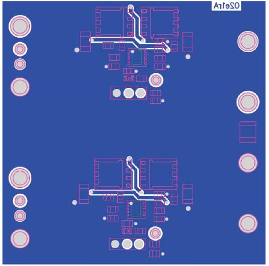
10 Figure a PI00-EVAL layout top layer. Scale.0: Figure b PI00-EVAL layout mid layer. Scale.0: Mechancial Drawing Vin Vaux Gnd J Q SL SL R C R J D IC R R R R Q FT Vout Vin Vaux Gnd PI00-EVAL Q IC R C R D J ra /00 R0 Q R R9 R FT Cool-ORing Gnd Picor Corporation PI00-EVAL User Guide Rev.0 Page 0 of
11 Vicor s comprehensive line of power solutions includes high-density AC-DC & DC-DC modules and accessory components, fully configurable AC-DC & DC-DC power supplies, and complete custom power systems. Information furnished by Vicor is believed to be accurate and reliable. However, no responsibility is assumed by Vicor for its use. No license is granted by implication or otherwise under any patent or patent rights of Vicor. Vicor components are not designed to be used in applications, such as life support systems, wherein a failure or malfunction could result in injury or death. All sales are subject to Vicor s Terms and Conditions of Sale, which are available upon request. Specifications are subject to change without notice. Vicor Corporation Frontage Road Andover, MA 00 USA Picor Corporation Industrial Drive North Smithfield, RI 09 USA Customer Service: custserv@vicorpower.com Technical Support: apps@vicorpower.com Tel: Fax: 9-- Picor Corporation PI00-EVAL User Guide Rev.0 Page of
PI2007-EVAL2 Cool-ORing Series
 PI2007-EVAL2 Cool-ORing Series PI2007-EVAL2 12V/15A High Side Active ORing Evaluation Board User Guide Content Page Cool-ORing Series Introduction... 1 Product Description... 2 Schematic... 3 Bill of Material...
Cool-ORing PI2007 Product Description
 PI2007-EVAL1 Cool-ORing Series PI2007-EVAL1 48V Bus High Side Active ORing Evaluation Board User Guide Content Page Cool-ORing Series Introduction... 1 Product Description... 2 Schematic... 3 Bill of Material...
PI2161-EVAL1 60V/12A High Side High Voltage Load Disconnect Switch Evaluation Board User Guide
 PI2161-EVAL1 Series PI2161-EVAL1 60V/12A High Side High Voltage Load Disconnect Switch Evaluation Board User Guide Content Page Introduction... 1 Product Description... 2 Schematic.... 2 Bill of Materials...
PI2122 Cool-ORing Series
 PI2122 Cool-ORing Series 12Amp Active ORing Solution With Load Disconnect Description The Cool-ORing PI2122 is a complete full-function Active ORing solution with a high-speed ORing MOSFET controller and
PI2002 Cool-ORing TM Series
 PI2002 Cool-ORing TM Series Active ORing Controller IC with Load Disconnect Feature Description The PI2002 Cool-ORing TM solution is a high-speed Active ORing controller IC with a load disconnect feature
PI2003 Series. Universal Active ORing Controller IC. Description. Features. Applications. Package Information. Typical Applications:
 Universal Active ORing Controller IC PI2003 Series Description The PI2003 solution is a universal highspeed Active ORing controller IC designed for use with N-channel MOSFETs and is optimized for -48V
QPI-5L. 14 Amp Active EMI Filter for 24 V DC Bus. Features. Description. Applications 查询 QPI-5L 供应商. QuietPower
 查询 5L 供应商 5L QuietPower 14 Amp Active EMI Filter for 24 V DC Bus Description The 5 active EMI filter attenuates conducted common-mode (CM) and differential-mode (DM) noise over the CISPR22 frequency range
High-Voltage, Overvoltage/ Undervoltage, Protection Switch Controller MAX6399
 General Description The is a small overvoltage and undervoltage protection circuit. The device can monitor a DC-DC output voltage and quickly disconnect the power source from the DC-DC input load when
MIC4414/4415. General Description. Features. Applications. Typical Application. 1.5A, 4.5V to 18V, Low-Side MOSFET Driver
 MIC4414/4415 1.5A, 4.5V to 18V, Low-Side MOSFET Driver General Description The MIC4414 and MIC4415 are low-side MOSFET drivers designed to switch an N-channel enhancement type MOSFET in low-side switch
Evaluates: MAX17552 (TDFN) in 5V Output Voltage Applications. MAX V Output Evaluation Kit (TDFN) General Description.
 in 5V Output Voltage Applications. MAX V Output Evaluation Kit (TDFN) General Description.") General Description The MAX7552 5V evaluation kit (EV kit) (TDFN) is a fully assembled and tested circuit board that demonstrates the performance of the MAX7552 60V, 00mA ultra-small, high-efficiency,
General Description The MAX7552 5V evaluation kit (EV kit) (TDFN) is a fully assembled and tested circuit board that demonstrates the performance of the MAX7552 60V, 00mA ultra-small, high-efficiency,
BCM Array TM BC384R120T030VM-00
 BCM Array TM BC384R120T030VM-00 Features 384 V to 12 V VI BRICK BCM Array 300 Watt (450 Watt for 1 ms) Vertical mount package reduces footprint Integrated heat sink simplifies thermal management ZVS /
QPI-AN1 GENERAL APPLICATION NOTE QPI FAMILY BUS SUPPLY QPI CONVERTER
 QPI-AN1 GENERAL APPLICATION NOTE QPI FAMILY EMI control is a complex design task that is highly dependent on many design elements. Like passive filters, active filters for conducted noise require careful
DC-DC Converter Module
 Features DC input range: 27-56 V Input surge withstand: 105 V for 100 ms DC output: 13.4 V Programmable output: 10 to 110% Regulation: ±0.2% no load to full load Efficiency: 88.5% Maximum operating temperature:
Low-Cost, High-Reliability, 0.5V to 3.3V ORing MOSFET Controllers
 3-3087; Rev 0; /04 EVALUATION KIT AVAILABLE Low-Cost, High-Reliability, 0.5V to 3.3V ORing General Description Critical loads often employ parallel-connected power supplies with redundancy to enhance system
Adjustable Current Limited Power Distribution Switch
 FEATURES 2.8V to 5.5V Operating Range Adjustable Current Limit : 200mA to 2.25A(Typ.) Fold-back Short Circuit Protection 130uA Typical On-State Supply Current 5uA Maximum Standby Supply Current Independent
AN1441 Application note
 Application note ST890: a high side switch for PCMCIA and USB applications Introduction The ST890 is a low voltage, P-channel MOSFET power switch, intended for high side load switching applications. Its
Intermediate Bus Converters Quarter-Brick, 48 Vin Family
 PRELIMINARY 45 V I Chip TM VIC-in-a-Brick Features Up to 600 W 95% efficiency @ 3 Vdc 600 W @ 55ºC, 400 LFM 125 C operating temperature 400 W/in 3 power density 38-55 Vdc input range 100 V input surge
MAXREFDES121# Isolated 24V to 3.3V 33W Power Supply
 System Board 6309 MAXREFDES121# Isolated 24V to 3.3V 33W Power Supply Maxim s power-supply experts have designed and built a series of isolated, industrial power-supply reference designs. Each of these
PI2007 Cool-ORing Series
 P007 Cool-ORing Series Universal High Side Active ORing Controller C Description The P007 Cool-ORing solution is a universal high-speed Active ORing controller C designed for use with N-channel MOSFETs
MAX8969 Evaluation Kit Evaluates: MAX8969
 General Description The MAX8969 evaluation kit (EV kit) is a fully assembled and tested PCB for evaluating the MAX8969 IC. The IC is a simple 1A step-up converter in a small package that can be used in
RT9728A. 120mΩ, 1.3A Power Switch with Programmable Current Limit. General Description. Features. Applications. Pin Configurations
 RT9728A 120mΩ, 1.3A Power Switch with Programmable Current Limit General Description The RT9728A is a cost effective, low voltage, single P-MOSFET high side power switch IC for USB application with a programmable
RT9728C. 120mΩ, 1.3A Power Switch with Programmable Current Limit. General Description. Features. Applications. Pin Configurations
 RT9728C 120mΩ, 1.3A Power Switch with Programmable Current Limit General Description The RT9728C is a cost effective, low voltage, single P-MOSFET high-side power switch IC for USB application with a programmable
Evaluation Board Manual
 SiP349, SiP349 Evaluation Board Manual DESCRIPTION SiP349 and SiP349 are a load switch that integrates multiple control features that simplify the design and increase the reliability of the circuitry connected
Evaluates: MAX6397. MAX6397 Evaluation Kit. General Description. Quick Start. Features. Ordering Information. Procedure
 General Description The MAX6397 evaluation kit (EV kit) demonstrates a high-voltage overvoltage protection circuit for applications that must survive load dump and high-voltage transient conditions. This
Figure 1: Over Voltage, Under Voltage, Over Current and Inrush Current Protection
 a) Over Voltage, Under Voltage, Over Current and Inrush Current Protection Figure 1: Over Voltage, Under Voltage, Over Current and Inrush Current Protection The protection is implemented using a controller.
Features MIC2193BM. Si9803 ( 2) 6.3V ( 2) VDD OUTP COMP OUTN. Si9804 ( 2) Adjustable Output Synchronous Buck Converter
 6.3V ( 2) VDD OUTP COMP OUTN. Si9804 ( 2) Adjustable Output Synchronous Buck Converter") MIC2193 4kHz SO-8 Synchronous Buck Control IC General Description s MIC2193 is a high efficiency, PWM synchronous buck control IC housed in the SO-8 package. Its 2.9V to 14V input voltage range allows
MIC2193 4kHz SO-8 Synchronous Buck Control IC General Description s MIC2193 is a high efficiency, PWM synchronous buck control IC housed in the SO-8 package. Its 2.9V to 14V input voltage range allows
Evaluates: MAX17532 (TDFN) in 5V Output Voltage Applications. MAX V Output Evaluation Kit (TDFN) General Description. Features.
 in 5V Output Voltage Applications. MAX V Output Evaluation Kit (TDFN) General Description. Features.") General Description The MAX753 5V evaluation kit (EV kit) (TDFN) is a fully assembled and tested circuit board that demonstrates the performance of the MAX753 4V, 00mA ultra-small, high-efficiency, synchronous
General Description The MAX753 5V evaluation kit (EV kit) (TDFN) is a fully assembled and tested circuit board that demonstrates the performance of the MAX753 4V, 00mA ultra-small, high-efficiency, synchronous
MIC5524. Features. General Description. Applications. Typical Application. High-Performance 500mA LDO in Thin DFN Package
 High-Performance 500mA LDO in Thin DFN Package General Description The is a low-power, µcap, low dropout regulator designed for optimal performance in a very-small footprint. It is capable of sourcing
Features MIC2010-1P/-2P MAIN AUX OUT1 EN2 FAULT1 GND. Figure 1. USB Wakeup From ACPI S3 System Diagram
 MIC2010/MIC2070 USB Power Controller General Description The MIC2010 is a dual channel USB power switch designed to support the power distribution requirements for USB Wakeup from the ACPI S3 state. The
PI LGIZ. 360μΩ, 5 V/60 A N-Channel MOSFET. μr DS(on) FET Series. Product Description. Features. Applications.
 FET Series. Product Description. Features. Applications.") μr DS(on) FET Series PI5101-01-LGIZ 3μΩ, 5 V/ A N-Channel MOSFET Product Description The PI5101μR DS (on) FET solution combines a highperformance 5 V, 3 μω lateral N-Channel MOSFET with a thermally enhanced
μr DS(on) FET Series PI5101-01-LGIZ 3μΩ, 5 V/ A N-Channel MOSFET Product Description The PI5101μR DS (on) FET solution combines a highperformance 5 V, 3 μω lateral N-Channel MOSFET with a thermally enhanced
Evaluation Board Manual
 SiP3249EVB, SiP32429EVB Evaluation Board Manual DESCRIPTION SiP3249EVB and SiP32429EVB are a load switch that integrates multiple control features that simplify the design and increase the reliability
+Denotes lead(pb)-free and RoHS compliant.
-free and RoHS compliant.") 19-4362; Rev 1; 3/09 MAX5963 Evaluation Kit General Description The MAX5963 evaluation kit (EV kit) circuit demonstrates the dual hot-swap, current-limit/circuit-breaker, and ORing functions of the MAX5963
19-4362; Rev 1; 3/09 MAX5963 Evaluation Kit General Description The MAX5963 evaluation kit (EV kit) circuit demonstrates the dual hot-swap, current-limit/circuit-breaker, and ORing functions of the MAX5963
SGM mA Buck/Boost Charge Pump LED Driver
 GENERAL DESCRIPTION The SGM3140 is a current-regulated charge pump ideal for powering high brightness LEDs for camera flash applications. The charge pump can be set to regulate two current levels for FLASH
Cool-Switch PI Volt, 12 Amp Full-Function Load Disconnect Switch Solution PI2161. Product Description. Features.
 Cool-Switch PI161 60 Volt, 1 Amp Full-Function Load Disconnect Switch Solution Product Description The Cool-Switch PI161 is a complete full-function Load Disconnect Switch solution for medium voltage applications
MIC5396/7/8/9. General Description. Features. Applications. Typical Application. Low-Power Dual 300mA LDO in 1.2mm x 1.
 Low-Power Dual 300mA LDO in 1.2mm x 1.6mm Extra Thin DFN General Description The is an advanced dual LDO ideal for powering general purpose portable devices. The provides two high-performance, independent
RT9728A. 120mΩ, 1.3A Power Switch with Programmable Current Limit. General Description. Features. Applications. Pin Configuration
 120mΩ, 1.3A Power Switch with Programmable Current Limit General Description The is a cost effective, low voltage, single P-MOSFET high-side power switch IC for USB application with a programmable current
VOUT = 5V VIN = 8V COUT CIN SENSE RPG EN/ UVLO OFF GND VOUT = 5V VIN = 8V CIN ADJ RPG EN/ UVLO OFF GND
 956-2 956-1 VIN = 8V OFF ON CIN 1µF R1 1kΩ R2 1kΩ + VIN EN/ UVLO GND VOUT SENSE PG + COUT 1µF VOUT = 5V RPG 1kΩ PG VIN = 8V OFF ON CIN 1µF R3 1kΩ R4 1kΩ + VIN EN/ UVLO GND VOUT ADJ PG R1 4.2kΩ R2 13kΩ
DISCONTINUED PRODUCT FOR REFERENCE ONLY.
 2525 AND 2535 Data Sheet 27447.B EN FLG GND 2 3 A2525EL GATE CONTROL 4 5 ABSOLUTE MAXIMUM RATINGS Supply Voltage, V IN... 6.0 V Output Voltage, V OUT... 6.0 V Output Current, I OUT... Internally Limited
STEF01. 8 V to 48 V fully programmable universal electronic fuse. Datasheet. Features. Applications. Description
 Datasheet 8 V to 48 V fully programmable universal electronic fuse Features HTSSOP14 Operating input voltage range: 8 to 48 V Absolute maximum input voltage: 55 V Continuous current typ.: 4 A N-channel
Discontinued Product
 Discontinued Product These parts are no longer in production The device should not be purchased for new design applications. Samples are no longer available. Date of status change: May 3, 2010 Recommended
SGM2576/SGM2576B Power Distribution Switches
 /B GENERAL DESCRIPTION The and B are integrated typically 100mΩ power switch for self-powered and bus-powered Universal Series Bus (USB) applications. The and B integrate programmable current limiting
Not Recommended for New Designs
 Not Recommended for New Designs B048F030T21 B048F030M21 BCM TM Bus Converter 48 V to 3 V V I Chip Bus Converter 210 Watt (315 Watt for 1 ms) High density 237 A/in 3 Small footprint 60 A/in 2 Low weight
Combo Hot Swap/Load Share Controller Allows the Use of Standard Power Modules in Redundant Power Systems
 Combo Hot Swap/Load Share Controller Allows the Use of Standard Power Modules in Redundant Power Systems by Vladimir Ostrerov and David Soo Introduction High power, high-reliability electronics systems
AIC bit DAC, Synchronous PWM Power Regulator with Dual Linear Controllers FEATURES DESCRIPTION APPLICATIONS
 5-bit DAC, Synchronous PWM Power Regulator with Dual Linear Controllers FEATURES Provides 3 Regulated Voltages for Microprocessor Core, Clock and GTL Power. Simple Voltage-Mode PWM Control. Dual N-Channel
RT2517B. 1A, 6V, Ultra-Low Dropout Linear Regulator. General Description. Features. Applications. Ordering Information. Marking Information
 RT2517B 1A, 6V, Ultra-Low Dropout Linear Regulator General Description The RT2517B is a high performance positive voltage regulator designed for use in applications requiring ultralow input voltage and
4.5V to 32V Input High Current LED Driver IC For Buck or Buck-Boost Topology CN5816. Features: SHDN COMP OVP CSP CSN
 4.5V to 32V Input High Current LED Driver IC For Buck or Buck-Boost Topology CN5816 General Description: The CN5816 is a current mode fixed-frequency PWM controller for high current LED applications. The
Automotive High Side TMOS Driver
 MOTOROLA SEMICONDUCTOR Automotive High Side TMOS Driver The D is a high side TMOS driver, dedicated for automotive applications. It is used in conjunction with an external power MOSFET for high side drive
Features MIC2194BM VIN EN/ UVLO CS OUTP VDD FB. 2k COMP GND. Adjustable Output Buck Converter MIC2194BM UVLO
 MIC2194 400kHz SO-8 Buck Control IC General Description s MIC2194 is a high efficiency PWM buck control IC housed in the SO-8 package. Its 2.9V to 14V input voltage range allows it to efficiently step
Purpose. Table of Contents. Purpose Introduction General Product Information Key Performance Summary Table... 3
 Purpose The RT8295A is a high-efficiency current mode synchronous step-down regulator that can deliver up to 2A output current from a wide input voltage range of 4.5V to 23V. This document explains the
Positive High-Voltage, Hot-Swap Controller
 9-36; Rev 0; /0 EVALUATION KIT AVAILABLE Positive High-Voltage, Hot-Swap Controller General Description The is a fully integrated hot-swap controller for +9V to +80V positive supply rails. The allows for
MAX16803EVKIT+BJT Evaluation Kit+
 19-0828; Rev 0; 5/07 MAX16803EVKIT+BJT Evaluation Kit+ General Description The MAX16803EVKIT+BJT (EV kit) demonstrates a high-current LED driver with accurate current control based on the MAX16803 current
USB High-Side Power Switch
 SP2525A USB High-Side Power Switch FEATURES +3.0V to +5.5V Input Voltage Range 500mA Continuous Load Current per Channel 2.6V Undervoltage Lockout.25A Short Circuit Current Limit 00mΩ Maximum On-Resistance
Evaluation Board for ADP2114 EVAL-ADP2114
 Evaluation Board for ADP EVAL-ADP FEATURES Full-featured demo board for the ADP Standalone capability Configurable dual synchronous step-down, dc-to-dc switching regulator Dual A/ A or A/ A output or single
BOOST/ BUCK-BOOST/ BUCK CONTROLLER IC with External MOSFET
 BOOST/ BUCK-BOOST/ BUCK CONTROLLER IC with External MOSFET FEATURES 5-60V input voltage range Single resistor programmable constant current driver Excellent constant current accuracy ±3% typically 0.1V
MIC23099 Evaluation Board
 Single AA/AAA Cell Step-Up/Step-Down Regulators with Battery Monitoring General Description The MIC23099 is a high-efficiency, low-noise, dual-output, integrated power-management solution for single-cell
EOL - Not Recommended for New Designs; Alternate Solution is B384F120T C baseplate operation. 384 V to 12 V Bus Converter
 BCM Bus Converter Advanced Sine Amplitude Converter (SAC ) Technology Size: 1.91 x 1.09 x 0.37 in 48,6 x 27,7 x 9,5 mm Features 100 C baseplate operation 384 V to 12 V Bus Converter 300 Watt ( 450 Watt
RT2517B. 1A, 6V, Ultra-Low Dropout Linear Regulator. Features. General Description. Applications. Ordering Information. Marking Information
 Sample & Buy 1A, 6V, Ultra-Low Dropout Linear Regulator General Description The is a high performance positive voltage regulator designed for use in applications requiring ultralow input voltage and ultra-low
MIC69101/103. General Description. Features. Applications. Typical Application. Single Supply V IN, LOW V IN, LOW V OUT, 1A LDO
 MIC6911/13 Single Supply V IN, LOW V IN, LOW V OUT, 1A LDO General Description The MIC6911/13 is the 1A output current member of the MIC69xxx family of high current, low voltage regulators, which support
MIC5316. General Description. Features. Applications. Typical Application. Low Voltage Dual 300mA LDO with Power on Reset and Voltage Select
 Low Voltage Dual 300mA LDO with Power on Reset and Voltage Select General Description The is a high performance, dual low input voltage, low dropout regulator with Power On Reset (POR) and voltage select.
Evaluates: MAXM V Output-Voltage Application. MAXM17532 Evaluation Kit. General Description. Quick Start. Features. Recommended Equipment
 General Description The MAXM17532 evaluation kit (EV kit) is a demonstration circuit of the MAXM17532 42V,0mA ultra-small, high efficiency, current mode, synchronous step-down DC-DC switching power module.
AIC1340 High Performance, Triple-Output, Auto- Tracking Combo Controller
 High Performance, Triple-Output, Auto- Tracking Combo Controller FEATURES Provide Triple Accurate Regulated Voltages Optimized Voltage-Mode PWM Control Dual N-Channel MOSFET Synchronous Drivers Fast Transient
RT9209/A. Synchronous Buck PWM DC-DC with Enable & PGOOD. Preliminary. Features. General Description. Applications. Ordering Information
 Preliminary Synchronous Buck PWM DC-DC with Enable & PGOOD General Description The is a single power supply PWM DC-DC converter controller designed to drive N-Channel MOSFET in a synchronous buck topology.
ABSOLUTE MAXIMUM RATINGS These are stress ratings only and functional operation of the device at these ratings or any other above those indicated in t
 SP2526 +3.0V to +5.5V USB Power Control Switch Compliant to USB Specifications +3.0V to +5.5V Input Voltage Range Two Independent Power Switches Two Error Flag Outputs, Open Drain 2.7V Undervoltage Lockout
November 2011 Rev FEATURES. Fig. 1: SP2526A Application Diagram Two Port Self Powered Hub
 November 2011 Rev. 2.1.0 GENERAL DESCRIPTION The SP2526A device is a dual +3.0V to +5.5V USB Supervisory Power Control Switch ideal for self-powered and bus-powered Universal Serial Bus (USB) applications.
Evaluates: MAX14691 MAX MAX14691 Evaluation Kit. General Description. Quick Start. Benefits and Features. Required Equipment.
 General Description The MAX469 evaluation kit (EV kit) is a fully assembled and tested circuit board that demonstrates the MAX469 overvoltage-, undervoltage-, and overcurrentprotection device. The EV kit
MIC4478/4479/4480. General Description. Features. Applications. Typical Application. 32V Low-Side Dual MOSFET Drivers
 32V Low-Side Dual MOSFET Drivers General Description The MIC4478, MIC4479, and MIC4480 are low-side dual MOSFET drivers are designed to switch N-channel enhancement type MOSFETs from TTL-compatible control
SGM2553/SGM2553D Precision Adjustable Current Limited Power Distribution Switches
 /D GENERAL DESCRIPTION The and D power distribution switches are intended for applications where precision current limiting is required or heavy capacitive loads and short circuits are encountered and
FAN5037. Adjustable Switching Regulator Controller. Features. Description. Applications. Block Diagram.
 Adjustable Switching Regulator Controller www.fairchildsemi.com Features High power switch-mode DC-DC controller can provide in excess of 13A Output voltage adjustable from 1.V to 3.6V 85% efficiency Cumulative
MIC2296. General Description. Features. Applications. High Power Density 1.2A Boost Regulator
 High Power Density 1.2A Boost Regulator General Description The is a 600kHz, PWM dc/dc boost switching regulator available in a 2mm x 2mm MLF package option. High power density is achieved with the s internal
Evaluates: MAX17544 in 5V Output-Voltage Application. MAX V Output Evaluation Kit. General Description. Features.
 MAX7544 5V Output Evaluation Kit Evaluates: MAX7544 in General Description The MAX7544 5V output evaluation kit (EV kit) provides a proven design to evaluate the MAX7544 high-voltage, high-efficiency,
RT A, Low Input Voltage, Ultra-Low Dropout LDO Regulator with Enable. Features. General Description. Applications. Ordering Information
 RT2516 2A, Low Input Voltage, Ultra-Low Dropout LDO Regulator with Enable General Description The RT2516 is a high performance positive voltage regulator designed for use in applications requiring ultra-low
AMS2115 FAST TRANSIENT RESPONSE LDO CONTROLLER
 FAST TRANSIENT RESPONSE LDO CONTROLLER General Description The AMS5 is a single IC controller that drives an external N Channel MOSFET as a source follower to produce a fast transient response, low dropout
High Efficiency 8A Synchronous Boost Convertor
 High Efficiency 8A Synchronous Boost Convertor General Description The is a synchronous current mode boost DC-DC converter. Its PWM circuitry with built-in 8A current power MOSFET makes this converter
RTQ2516-QT. 2A, Low Input Voltage, Ultra-Low Dropout LDO Regulator with Enable. General Description. Features. Applications. Ordering Information
 RTQ2516-QT 2A, Low Input Voltage, Ultra-Low Dropout LDO Regulator with Enable General Description The RTQ2516 is a high performance positive voltage regulator designed for use in applications requiring
MP A, 36V, 700KHz Step-Down Converter with Programmable Output Current Limit
 The Future of Analog IC Technology MP2490 1.5A, 36V, 700KHz Step-Down Converter with Programmable Output Current Limit DESCRIPTION The MP2490 is a monolithic step-down switch mode converter with a programmable
Features. Applications. 1.2MHz Boost Converter with OVP in Thin SOT-23-6
 1.2MHz PWM Boost Converter with OVP General Description The is a 1.2MHz pulse width modulated (PWM) step-up switching regulator that is optimized for low power, high output voltage applications. With a
MIC3975. General Description. Features. Applications. Ordering Information. Typical Applications. 750mA µcap Low-Voltage Low-Dropout Regulator
 MIC3975 750mA µcap Low-Voltage Low-Dropout Regulator General Description The MIC3975 is a 750mA low-dropout linear voltage regulators that provide low-voltage, high-current output from an extremely small
Enpirion EN5364QI 6A and EN5394QI 9A DCDC Converter w/integrated Inductor Evaluation Board
 Enpirion EN5364QI 6A and EN5394QI 9A DCDC Converter w/integrated Inductor Evaluation Board Introduction Thank you for choosing Enpirion, the source for Ultra small foot print power converter products.
TOP VIEW. OUTPUT PRESET 2.5V TO 5V 200mA SHDN 3 4 BP GND. Maxim Integrated Products 1
 19-2584; Rev ; 1/2 Low-Noise, Low-Dropout, 2mA General Description The low-noise, low-dropout linear regulator operates from a 2.5V to 6.5V input and delivers up to 2mA. Typical output noise is 3µV RMS,
ML4818 Phase Modulation/Soft Switching Controller
 Phase Modulation/Soft Switching Controller www.fairchildsemi.com Features Full bridge phase modulation zero voltage switching circuit with programmable ZV transition times Constant frequency operation
A8431. White LED Driver Constant Current Step-up Converter
 Features and Benefits Output voltage up to 32 V ( level) 2. to 0 V input Drives up to 4 LEDs at 20 ma from a 2. V supply Drives up to LEDs at 20 ma from a 3 V supply.2 MHz switching frequency 300 ma switch
RT9059A. 3A, Ultra-Low Dropout Voltage Regulator. General Description. Features. Applications. Ordering Information. Marking Information
 RT9059A 3A, Ultra-Low Dropout Voltage Regulator General Description The RT9059A is a high performance positive voltage regulator designed for use in applications requiring very low input voltage and very
Is Now Part of To learn more about ON Semiconductor, please visit our website at
 Is Now Part of To learn more about ON Semiconductor, please visit our website at www.onsemi.com ON Semiconductor and the ON Semiconductor logo are trademarks of Semiconductor Components Industries, LLC
RT9807. Micro-Power Voltage Detector with Manual Reset. General Description. Features. Applications. Pin Configurations. Ordering Information RT9807-
 Micro-Power Voltage Detector with Manual Reset General Description The is a micro-power voltage detector with deglitched manual reset input which supervises the power supply voltage level for microprocessors
User s Manual ISL15102IRZ-EVALZ. User s Manual: Evaluation Board. Industrial Analog and Power
 User s Manual ISL1512IRZ-EVALZ User s Manual: Evaluation Board Industrial Analog and Power Rev. Nov 217 USER S MANUAL ISL1512IRZ-EVALZ Evaluation Board UG151 Rev.. 1. Overview The ISL1512IRZ-EVAL board
Evaluation Board for ADP2118 EVAL-ADP2118
 Evaluation Board for ADP8 EVAL-ADP8 GENERAL DESCRIPTION The evaluation (demo) board provides an easy way to evaluate the ADP8 buck regulator. This data sheet describes how to quickly set up the board to
AME. Low Dropout 2A CMOS Regulator AME8882. n General Description. n Typical Application. n Features. n Functional Block Diagram.
 8882 n General Description n Typical Application The 8882A/B family of positive CMOS linear regulators provides ultra low-dropout voltage (240mV @2A) and low quiescent current (typically 600uA), thus making
MIC2196. Features. General Description. Applications. Typical Application. 400kHz SO-8 Boost Control IC
 400kHz SO-8 Boost Control IC General Description Micrel s is a high efficiency PWM boost control IC housed in a SO-8 package. The is optimized for low input voltage applications. With its wide input voltage
MP A, 55V, 100kHz Step-Down Converter with Programmable Output OVP Threshold
 The Future of Analog IC Technology MP24943 3A, 55V, 100kHz Step-Down Converter with Programmable Output OVP Threshold DESCRIPTION The MP24943 is a monolithic, step-down, switch-mode converter. It supplies
MP V to 5.5V Input, 1.2MHz, Dual-ch LCD Bias Power Supply
 MP5610 2.7V to 5.5V Input, 1.2MHz, Dual-ch LCD Bias Power Supply DESCRIPTION The MP5610 is a dual-output converter with 2.7V-to-5.5V input for small size LCD panel bias supply. It uses peak-current mode
MIC General Description. Features. Applications. Typical Application. 5A, Low V IN, Low V OUT µcap LDO Regulator
 MIC6952, Low V IN, Low V OUT µcap LDO Regulator General Description The MIC6952 is a, low dropout linear regulator that provides low voltage high current outputs with a minimum of external components.
Evaluates: MAX17761 in 5V Output-Voltage Application. MAX V Output Evaluation Kit. General Description. Quick Start.
 General Description The MAX17761 5V output EV kit is a proven design to evaluate the MAX17761 high-efficiency, high-voltage, synchronous step-down DC-DC converter in a TDFN package. The EV kit generates
RT9202. Single Synchronous Buck PWM DC-DC Controller. General Description. Features. Applications. Ordering Information. Pin Configurations
 Single Synchronous Buck PWM DC-DC Controller General Description The is a single power supply PWM DC-DC converter controller designed to drive N-Channel MOSFET in a synchronous buck topology. The IC integrates
Low Cost 8W Off-line LED Driver using RT8487
 Application Note AN019 Jun 2014 Low Cost 8W Off-line LED Driver using RT8487 Abstract RT8487 is a boundary mode constant current controller with internal high side driver, which can be used in buck and
WD3119 WD3119. High Efficiency, 40V Step-Up White LED Driver. Descriptions. Features. Applications. Order information 3119 FCYW 3119 YYWW
 High Efficiency, 40V Step-Up White LED Driver Http//:www.sh-willsemi.com Descriptions The is a constant current, high efficiency LED driver. Internal MOSFET can drive up to 10 white LEDs in series and
Logic Controlled, High-Side Power Switch with Reverse Current Blocking ADP195
 Data Sheet Logic Controlled, High-Side Power Switch with Reverse Current Blocking ADP95 FEATURES Ultralow on resistance (RDSON) 5 mω @.6 V 55 mω @.5 V 65 mω @.8 V mω @. V Input voltage range:. V to.6 V.
Fault Management Circuit
 APPLICATION NOTE AN:033 Ankur Patel Applications Engineering September 2015 Contents Page Introduction 1 Concept and Design 1 Considerations Component Selection 4 Equations 5 Example 5 Conclusion 6 Introduction
HM2259D. 2A, 4.5V-20V Input,1MHz Synchronous Step-Down Converter. General Description. Features. Applications. Package. Typical Application Circuit
 HM2259D 2A, 4.5V-20V Input,1MHz Synchronous Step-Down Converter General Description Features HM2259D is a fully integrated, high efficiency 2A synchronous rectified step-down converter. The HM2259D operates
MIC69151/153. General Description. Features. Applications. Typical Application. Single Supply V IN, Low V IN, Low V OUT, 1.5A LDO
 Single Supply V IN, Low V IN, Low V OUT, 1.5A LDO General Description The is the 1.5A output current member of the MIC69xxx family of high current, low voltage regulators, which support currents of 1A,
MP V, 700kHz Synchronous Step-Up White LED Driver
 The Future of Analog IC Technology MP3306 30V, 700kHz Synchronous Step-Up White LED Driver DESCRIPTION The MP3306 is a step-up converter designed for driving white LEDs from 3V to 12V power supply. The