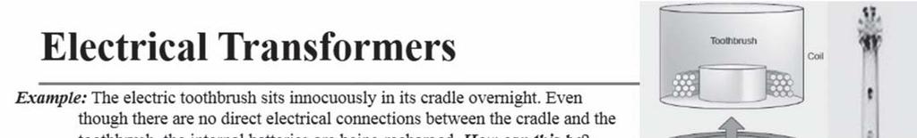
For the circuit in Fig. 1, determine the current in the neutral line.
|
|
|
- Garey Joseph
- 5 years ago
- Views:
Transcription


1
2 Problem 1 For the circuit in Fig. 1, determine the current in the neutral line. Solution Figure 1 Since the neutral line is present, we can solve this problem on a per-phase basis. For phase a, For phase b, For phase c, I I I a b c = Van = = 6.55 Z 2 27 j A Vbn = = = Z 2 22 B = Vcn = = Z 2 12 j C The current in the neutral line is I n = -( I a I b I c ) or - I = I I I n a b c - I n = (5.263 j3.9) (-5 j8.66) ( j16.78) I n = 1.91 j = A
3 Problem 2 Solve for the line currents in the Y- circuit of Fig. 2. Take Z = Ω. Figure 2 Solution Convert the delta-load to a Wye-load and apply per-phase analysis V - I a Z Y Z Y = Z 3 = Ω I a = = A I I = -120 = A b I a = 120 = A c I a
4 Problem 3 Find the line currents I a, I b, and I c in the three-phase network of Fig. 3 below. Take Z = 12 - j15ω, Z Y = 4 j6 Ω, and Z l = 2 Ω. Solution Figure Convert the D-connected source to a Y-connected source. V p 208 V an = - 30 = - 30 = Convert the D-connected load to a Y-connected load. Z (4 j6)(4 j5) Z = Z Y = (4 j6) (4 j5) = 3 8 j Z = j Z L I a V an - Z I a = Z V L an Z = = A j I I = -120 = A b I a = 120 = A c I a
5 Problem 4 In the circuit of Fig. 4, if V ab = , V bc = , V ca = V, find the line currents. Figure Solution Convert the delta-connected source to an equivalent wye-connected source and consider the single-phase equivalent. I a = 440 (10 30 ) 3 Z Y where Z = 3 j2 10 j8 = 13 j6 = Y I a = = A 3 ( ) I I = -120 = A b I a = 120 = A c I a
6 Problem 5 The following three parallel-connected three-phase loads are fed by a balanced threephase source. Load 1: 250 kva, 0.8 pf lagging Load 2: 300 kva, 0.95 pf leading Load 3: 450 kva, unity pf If the line voltage is 13.8 kv, calculate the line current and the power factor of the source. Assume that the line impedance is zero. Solution pf -1 S = 0.8 (lagging) θ = cos (0.8) = = = 200 j150 kva 1 pf -1 S = 0.95 (leading) θ = cos (0.95) = = = 285 j93.65 kva 2-1 pf = 1.0 θ = cos (1) = 0 S = kva S = 935 j56.35 = T = S1 S 2 S 3 kva S T = 3 V L I L I L = = 3 3 ( ) A rms pf = cosθ = cos(3.45 ) = (lagging)
7 Problem 6 A professional center is supplied by a balanced three-phase source. The center has four plants, each a balanced three-phase load as follows: Load 1: 150 kva at 0.8 pf leading Load 2: 100 kw at unity pf Load 3: 200 kva at 0.6 pf lagging Load 4: 80 kw and 95 kvar (inductive) If the line impedance is 0.02 j0.05 Ω per phase and the line voltage at the loads is 480 V, find the magnitude of the line voltage at the source. Solution pf = 0.8 (leading) θ1 = S = kva 1 pf = 1.0 θ2 = 0 S = kva 2 pf = 0.6 (lagging) θ3 = S = kva 3 S 4 = 80 j95 kva S = S1 S 2 S 3 S 4 S = 420 j165 = kva S = 3 V L I L 3 S I L = = = A 3 VL For the line, 2 2 S L = 3I L Z L = (3)(542.7) (0.02 j0.05) S L = j44.18 kva At the source, S T = S S L = j209.2 S T = kva 3 ST VT = = = 516 V 3 I L
8 Problem 7. Find the magnitude and phase angle of currents I a, I b, I c and I n if V = V 0, V = V = 440 Volts. an p L ab n Neutral Connected Solution We first find the magnitude of the various currents. S 4000 For the motor: I L = = = A 3 VL Q c 1800 For the capacitor: IC = = = A VL PLi 800 For the lighting: V p = = 254 V I Li = = = 3.15 A 3 Vp 254 Consider the figure below.
9 a I a I C I 1 b V ab I b -jx C I 2 c I c I Li I 3 n Vab If V an = V p 0, V ab = 3 V p 30 V cn = V p 120 I C = = jx C V I1 = ab = ( θ 30 ) where θ = cos -1 (0.72) = Z I = I = I = Vcn I Li = = Thus, R 2 I = I I = I = A a 1 C I = I I = I = A b 2 C I = I I = I = A c 3 I n = -I Li Li I n = A R 3 a b c


10


11


12


13


14


15


16


17


18


19


20

21

22


23


24


25


26


27


28


29


30


31


32


33


34


35


36


37


38


39


40


41


42


43


44


45


46


47 Electrical Engineering Dept. CIRCUIT ANALYSIS Hayt, Kimmerly & Durbin Z.R.K. JU EE-212 Z.R.K. JU EE-212
48 Z.R.K. JU EE-212 Z.R.K. JU EE-212
49 Z.R.K. JU EE-212 Z.R.K. JU EE-212
50 Z.R.K. JU EE-212 Z.R.K. JU EE-212
51 Z.R.K. JU EE-212 Z.R.K. JU EE-212
52 Z.R.K. JU EE-212 v t Z.R.K. JU EE-212
53 Z.R.K. JU EE-212 o. Z.R.K. JU EE-212
54 n Z.R.K. JU EE-212
55 EXERCISES 523 The dot convention allows a sign to be assigned to the mutual inductance term. (Example 13.1) According to the dot convention, a current entering the dotted terminal of one coil produces an open-circuit voltage with a positive voltage reference at the dotted terminal of the second coil. (Examples 13.1, 13.2, 13.3) The total energy stored in a pair of coupled coils has three separate terms: the energy stored in each self-inductance ( 1 2 Li2 ), and the energy stored in the mutual inductance (Mi 1 i 2 ). (Example 13.4) The coupling coefficient is given by k = M/ L 1 L 2, and is restricted to values between 0 and 1. (Example 13.4) A linear transformer consists of two coupled coils: the primary winding and the secondary winding. (Examples 13.5, 13.6) An ideal transformer is a useful approximation for practical iron-core transformers. The coupling coefficient is taken to be unity, and the inductance values are assumed to be infinite. (Examples 13.7, 13.8) The turns ratio a = N 2 /N 1 of an ideal transformer relates the primary and secondary coil voltages: V 2 = av 1. (Example 13.8) The turns ratio a also relates the currents in the primary and secondary coils: I 1 = ai 2. (Examples 13.7, 13.8) READING FURTHER Almost everything you ever wanted to know about transformers can be found in: M. Heathcote, J&P Transformer Book, 12th ed. Oxford: Reed Educational and Professional Publishing Ltd., Another comprehensive transformer title is: W. T. McLyman, Transformer and Inductor Design Handbook, 3rd ed. New York: Marcel Dekker, A good transformer book with a strong economic focus is: B. K. Kennedy, Energy Efficient Transformers. New York: McGraw-Hill, EXERCISES 13.1 Mutual Inductance 1. Consider the two inductances depicted in Fig Set L 1 = 10 mh, L 2 = 5 mh, and M = 1 mh. Determine the steady-state expression for (a) v 1 if i 1 = 0 and i 2 = 5 cos 8t A; (b) v 2 if i 1 = 3 sin 100t A and i 2 = 0; (c) v 2 if i 1 = 5 cos (8t 40 ) A and i 2 = 4 sin 8t A. i 1 i 2 M v 1 L 1 L 2 v 2 FIGURE 13.35
56 524 CHAPTER 13 MAGNETICALLY COUPLED CIRCUITS i 1 i 2 M v 1 L 1 L 2 FIGURE v 2 2. With respect to Fig , assume L 1 = 400 mh, L 2 = 230 mh, and M = 10 mh. Determine the steady-state expression for (a) v 1 if i 1 = 0 and i 2 = 2 cos 40t A; (b) v 2 if i 1 = 5 cos (40t 15 ) A and i 2 = 0. (c) Repeat parts (a) and (b) if M is increased to 300 mh. 3. In Fig , set L 1 = 1 μh, L 2 = 2 μh, and M = 150 nh. Obtain a steadystate expression for (a) v 1 if i 2 = cos 70t ma and i 1 = 0; (b) v 2 if i 1 = 55 cos (5t 30 ) A; (c) v 2 if i 1 = 6 sin 5t A and i 2 = 3 sin 5t. i 1 i 2 M v 1 L 1 L 2 v 2 i 1 i 2 M v 1 L 1 L 2 FIGURE v 2 FIGURE For the configuration of Fig , L 1 = 0.5L 2 = 1 mh and M = 0.85 L 1 L 2. Calculate v 2 (t) if (a) i 2 = 0 and i 1 = 5e t ma; (b) i 2 = 0 and i 1 = 5 cos 10t ma; (c) i 2 = 5 cos 70t ma and i 1 = 0.5i The physical construction of three pairs of coupled coils is shown in Fig Show the two different possible locations for the two dots on each pair of coils (a) 4 FIGURE (b) 3 4 (c) 6. In the circuit of Fig , i 1 = 5 sin (100t 80 ) ma, L 1 = 1 H, and L 2 = 2 H. If v 2 = 250 sin (100t 80 ) mv, calculate M. M i 1 L 1 L 2 v 2 FIGURE In the circuit represented in Fig , determine i 1 if v 2 (t) = 4 cos 5t V, L 1 = 1 mh, L 2 = 4 mh, and M = 1.5 mh. 8. Calculate v 1 and v 2 if i 1 = 5 sin 40t ma and i 2 = 5 cos 40t ma, L 1 = 1 mh, L 2 = 3 mh, and M = 0.5 mh, for the coupled inductances shown in (a) Fig ; (b) Fig
57 EXERCISES Calculate v 1 and v 2 if i 1 = 3 cos (2000t 13 ) ma and i 2 = 5 sin 400t ma, L 1 = 1 mh, L 2 = 3 mh, and M = 200 nh, for the coupled inductances shown in (a) Fig ; (b) Fig For the circuit of Fig , calculate I 1, I 2, V 2 V 1, and I 2 I k j V 1 = 40 0 V I 1 I 2 j2 k j1.8 k V FIGURE For the circuit of Fig , plot the magnitude of V 2 V 1 as a function of frequency ω, over the range 0 ω 2 rad/s. 1 j2 1 V 1 = 40 0 V I 1 I 2 j4 j6 V 2 1 FIGURE For the circuit of Fig , (a) draw the phasor representation; (b) write a complete set of mesh equations; (c) calculate i 2 (t) if v 1 (t) = 8 sin 720t V mf i 1 v i 2 i mh 2 mh 2 FIGURE M = 500 nh 13. In the circuit of Fig , M is reduced by an order of magnitude. Calculate i 3 if v 1 = 10 cos (800t 20 ) V. 14. In the circuit shown in Fig , find the average power absorbed by (a) the source; (b) each of the two resistors; (c) each of the two inductances; (d) the mutual inductance H M 2 cos 10t V 5 H 3 H 5 15 cos 200t V 15 mh 3 mh 8 (speaker) FIGURE FIGURE The circuit of Fig is designed to drive a simple 8 speaker. What value of M results in 1 W of average power being delivered to the speaker?
58 526 CHAPTER 13 MAGNETICALLY COUPLED CIRCUITS 16. Consider the circuit of Fig The two sources are i s1 = 2 cos t ma and i s2 = 1.5 sin t ma. If M 1 = 2 H, M 2 = 0 H, and M 3 = 10 H, calculate v AG (t). A B M 2 3 H i s2 i s1 20 H M 1 C M 3 5 H FIGURE G 17. For the circuit of Fig , M 1 = 1 H, M 2 = 1.5 H, and M 3 = 2 H. If i s1 = 8 cos 2t A and i s2 = 7 sin 2t A, calculate (a) V AB ; (b) V AG ; (c) V CG. 18. For the circuit of Fig , find the currents i 1 (t), i 2 (t), and i 3 (t) if f = 60 Hz. 5 I 2 4 H 2 i 1 v B M i 2 2 sin 3t V 3 H I 1 10 H I 3 12 v A L 1 L 2 FIGURE (a) 19. Determine an expression for i C (t) valid for t > 0 in the circuit of Fig , if v s (t) = 10t 2 u(t)/(t ) V. V 1 I A I B L 1 M 15 mh v s 10 mh 40 mh FIGURE v x 100v x i C 1 F V 2 L 2 (b) FIGURE For the coupled inductor network of Fig a, set L 1 = 20 mh, L 2 = 30 mh, M = 10 mh, and obtain equations for v A and v B if (a) i 1 = 0 and i 2 = 5 sin 10t; (b) i 1 = 5 cos 20t and i 2 = 2 cos (20t 100 ) ma. (c) Express V 1 and V 2 as functions of I A and I B for the network shown in Fig b.
59 EXERCISES Note that there is no mutual coupling between the 5 H and 6 H inductors in the circuit of Fig (a) Write a set of equations in terms of I 1 ( jω), I 2 ( jω), and I 3 ( jω). (b) Find I 3 ( jω) if ω = 2 rad/s. 4 4 H 3 H 2 H I V 5 H 0 H 6 6 H I 3 5 I 1 FIGURE Find V 1 ( jω) and V 2 ( jω) in terms of I 1 ( jω) and I 2 ( jω) for each circuit of Fig I 1 M I 2 I 1 I 2 R 1 R 2 R M 1 R 2 V 1 L 1 L 2 V 2 V 1 L 1 L 2 V 2 (a) FIGURE (b) H Z in 0.1 H 0.5 H (a) Find Z in ( jω) for the network of Fig (b) Plot Z in over the frequency range of 0 ω 1000 rad/s. (c) Find Z in ( jω) for ω = 50 rad/s Energy Considerations 24. For the coupled coils of Fig , L 1 = L 2 = 10 H, and M is equal to its maximum possible value. (a) Compute the coupling coefficient k. (b) Calculate the energy stored in the magnetic field linking the two coils at t = 200 ms if i 1 = 10 cos 4t ma and i 2 = 2 cos 4t ma. 25. With regard to the coupled inductors shown in Fig , L 1 = 10 mh, L 2 = 5 mh, and k = (a) Compute M. (b) If i 1 = 100 sin 40t ma, and i 2 = 0, compute the energy stored in each coil and in the magnetic field coupling the two inductors at t = 2 ms. (c) Repeat part (b) if i 2 is set to 75 cos 40t ma. 26. For the circuit of Fig , L 1 = 2 mh, L 2 = 8 mh, and v 1 = cos 8t V. (a) Obtain an equation for v 2 (t). (b) Plot V 2 as a function of k. (c) Plot the phase angle (in degrees) of V 2 as a function of k. FIGURE i 1 i 2 v 1 L 1 FIGURE L 2 v 2 M v 1 v 2 FIGURE k
60 528 CHAPTER 13 MAGNETICALLY COUPLED CIRCUITS 27. Connect a load Z L = 5/33 to the right-hand terminals of Fig Derive an expression for the input impedance at f = 100 Hz, seen looking into the lefthand terminals, if L 1 = 1.5 mh, L 2 = 3 mh, and k = Consider the circuit represented in Fig The coupling coefficient k = If i s = 5 cos 200t ma, calculate the total energy stored at t = 0 and t = 5 ms if (a) a-b is open-circuited (as shown); (b) a-b is short-circuited. 3 mh M a b i s 1.2 mh 12 mh 100 m FIGURE Compute v 1, v 2, and the average power delivered to each resistor in the circuit of Fig k 1 = H 1 H v cos 5t V 1 H 1 H v 2 2 FIGURE k 2 = The Linear Transformer 30. Assume the following values for the circuit depicted schematically in Fig : R 1 = 10, R 2 = 1, L 1 = 2 μh, L 2 = 1 μh, and M = 500 nh. Calculate the input impedance for ω = 10 rad/s if Z L is equal to (a) 1 ; (b) j ; (c) j ; (d) 5/ Determine the T equivalent of the linear transformer represented in Fig (draw and label an appropriate diagram). A i 1 i 2 25 nh C 130 nh 13 nh A B i 1 i 2 1 H 25 H FIGURE H C D B FIGURE D 32. (a) Draw and label an appropriate diagram of a T equivalent network for the linear transformer shown in Fig (b) Verify the two are equivalent by connecting a voltage v AB = 5 sin 45t V and calculating the open-circuit voltage v CD.
61 EXERCISES Represent the T network shown in Fig as an equivalent linear transformer if (a) L x = 1 H, L y = 2 H, and L z = 4 H; (b) L x = 10 mh, L y = 50 mh, and L z = 22 mh. A i 1 L x L y i 2 C L z B FIGURE D 34. Assuming zero initial currents, obtain an equivalent network of the transformer depicted in Fig (a) Draw and label a suitable equivalent network of the linear transformer shown in Fig , assuming zero initial currents. (b) Verify their equivalence with an appropriate simulation. 36. Represent the network of Fig as an equivalent linear transformer with zero initial currents if (a) L A = 1 H, L B = 2 H, and L C = 4 H; (b) L A = 10 mh, L B = 50 mh, and L C = 22 mh. i 1 i 2 A L B C L A L C B FIGURE D 37. For the circuit of Fig , determine an expression for (a) I L V s ; (b) V 1 V s. v s H 2 H 8 H 2 i L v 1 FIGURE (a) For the circuit of Fig , if v s = 8 cos 1000t V, calculate v o. (b) Verify your solution with an appropriate PSpice simulation. v s k = k = 1 10 mh 25 mh 5 mh 10 v o 50 mh FIGURE 13.62
62 530 CHAPTER 13 MAGNETICALLY COUPLED CIRCUITS M With respect to the network shown in Fig , derive an expression for Z( jω) if M 1 and M 2 are set to their respective maximum values. Z( j ) 1 H M 2 5 H 3 H The Ideal Transformer 40. Calculate I 2 and V 2 for the ideal transformer circuit of Fig if (a) V 1 = 4/32 V and Z L = 1 j ; (b) V 1 = 4/32 V and Z L = 0; (c) V 1 = 2/118 V and Z L = 1.5/ mh 500 mh 1 : 6 FIGURE V 1 I 1 I 2 Z L V 2 FIGURE With respect to the ideal transformer circuit depicted in Fig , calculate I 2 and V 2 if (a) I 1 = 244/0 ma and Z L = 5 j2 ;(b) I 1 = 100/10 ma and Z L = j Calculate the average power delivered to the 400 m and 21 resistors, respectively, in the circuit of Fig m 1 : cos 280t V i 1 i 2 v 1 v 2 21 FIGURE With regard to the ideal transformer circuit represented in Fig , determine an equivalent circuit in which (a) the transformer and primary circuit are replaced, so that V 2 and I 2 are unchanged; (b) the transformer and secondary circuit are replaced, so that V 1 and I 1 are unchanged. 44. Calculate the average power delivered to each resistor shown in Fig :9 1:4 5 cos 120 t A FIGURE With respect to the circuit depicted in Fig , calculate (a) the voltages v 1 and v 2 ; (b) the average power delivered to each resistor :1 2:15 25 cos 120 t ma 2.7 k v 1 v FIGURE 13.67
63 EXERCISES Calculate I x and V 2 as labeled in Fig I x : V V FIGURE The ideal transformer of the circuit in Fig is removed, flipped across its vertical axis, and reconnected such that the same terminals remain connected to the negative terminal of the source. (a) Calculate I x and V 2. (b) Repeat part (a) if both dots are placed at the bottom terminals of the transformer. 48. For the circuit of Fig , v s = 117 sin 500t V. Calculate v 2 if the terminals marked a and b are (a) left open-circuited; (b) short-circuited; (c) bridged by a 2 resistor. 49. The turns ratio of the ideal transformer in Fig is changed from 30:1 to 1:3. Take v s = 720 cos 120πt V, and calculate v 2 if terminals a and b are (a) short-circuited; (b) bridged by a 10 resistor; (c) bridged by a 1 M resistor. 50. For the circuit of Fig , R 1 = 1, R 2 = 4, and R L = 1. Select a and b to achieve a peak voltage of 200 V magnitude across R L. v s 1 FIGURE a 30:1 b v 2 4 R 1 R 1:1 2 i a:b L 2 cos 10t V 1.85 v x R L FIGURE Calculate v x for the circuit of Fig if a = 0.01b = 1, R 1 = 300, R 2 = 14, and R L = 1 k. 52. (a) Referring to the ideal transformer circuit in Fig , determine the load current i L if b = 0.25a = 1, R 1 = 2.2, R 2 = 3.1, and R L = 200. (b) Verify your solution with an appropriate PSpice simulation. 53. Determine the Thévenin equivalent of the network in Fig as seen looking into terminals a and b. 54. Calculate V 2 and the average power delivered to the 8 resistor of Fig if V s = 10/15 V, and the control parameter c is equal to (a) 0; (b) 1 ms. a 1 b I x FIGURE :2 3 10I x 2 a:b V s cv 2 8 V 2 FIGURE 13.72
64 532 CHAPTER 13 MAGNETICALLY COUPLED CIRCUITS 55. (a) For the circuit of Fig , take c = 2.5 ms and select values of a and b such that 100 W average power is delivered to the 8 load when V s = 5/35 V, (b) Verify your solution with an appropriate PSpice simulation. Chapter-Integrating Exercises 56. A transformer whose nameplate reads 2300/230 V, 25 kva operates with primary and secondary voltages of 2300 V and 230 V rms, respectively, and can supply 25 kva from its secondary winding. If this transformer is supplied with 2300 V rms and is connected to secondary loads requiring 8 kw at unity PF and 15 kva at 0.8 PF lagging, (a) what is the primary current? (b) How many kilowatts can the transformer still supply to a load operating at 0.95 PF lagging? (c) Verify your answers with PSpice. 57. A friend brings a vintage stereo system back from a recent trip to Warnemünde, unaware that it was designed to operate on twice the supply voltage (240 VAC) available at American household outlets. Design a circuit to allow your friend to listen to the stereo in the United States, assuming the operating frequency (50 Hz in Germany, 60 Hz in the United States) difference can be neglected. 58. The friend referred to in Exercise 57 attempts to justify the erroneous assumption made regarding the stereo by pointing out that the wall outlet in the W.C. (bathroom) had a socket for his U.S. electric razor, clearly marked 120 VAC. He failed to notice that the small sign below the outlet clearly stated Razors only. With the knowledge that all power lines running into the room operated at 240 VAC, draw the likely circuit built into the bathroom wall outlet, and explain why it is limited to razors only. 59. Obtain an expression for V 2 V s in the circuit of Fig if (a) L 1 = 100 mh, L 2 = 500 mh, and M is its maximum possible value; (b) L 1 = 5L 2 = 1.4 H and k = 87% of its maximum possible value; (c) the two coils can be treated as an ideal transformer, the left-hand coil having 500 turns and the right-hand coil having 10,000 turns. 5 V s L 1 L 2 40 V 2 FIGURE You notice your neighbor has installed a large coil of wire in close proximity to the power line coming into your house (underground cables are not available in your neighborhood). (a) What is the likely intention of your neighbor? (b) Is the plan likely to succeed? Explain. (c) When confronted, your neighbor simply shrugs and claims there s no way it can cost you anything, anyway, since nothing of his is touching anything on your property. True or not? Explain.
65 598 Chapter 13 Magnetically Coupled Circuits Review Questions 13.1 Refer to the two magnetically coupled coils of Fig (a). The polarity of the mutual voltage is: (a) Positive (b) Negative 13.6 For the ideal transformer in Fig (b), N 2 N The ratio I 2 I 1 is: (a) 10 (b) 0.1 (c) 0.1 (d) 10 i 1 M i 2 i 1 M i A three-winding transformer is connected as portrayed in Fig (a). The value of the output voltage is: V o (a) 10 (b) 6 (c) 6 (d) 10 (a) Figure For Review Questions 13.1 and (b) 50 V 2 V 8 V V o 50 V 2 V 8 V V o 13.2 For the two magnetically coupled coils of Fig (b), the polarity of the mutual voltage is: (a) Positive (b) Negative (a) Figure For Review Questions 13.7 and (b) 13.3 The coefficient of coupling for two coils having L 1 2 H, L 2 8 H, M 3 H is: (a) (b) 0.75 (c) (d) If the three-winding transformer is connected as in Fig (b), the value of the output voltage is: (a) 10 (b) 6 (c) 6 (d) 10 V o 13.4 A transformer is used in stepping down or stepping up: (a) dc voltages (b) ac voltages (c) both dc and ac voltages 13.5 The ideal transformer in Fig (a) has N 2 N The ratio V 2 V 1 is: (a) 10 (b) 0.1 (c) 0.1 (d) In order to match a source with internal impedance of 500 to a 15- load, what is needed is: (a) step-up linear transformer (b) step-down linear transformer (c) step-up ideal transformer (d) step-down ideal transformer (e) autotransformer I 1 N 1 : N 2 I 2 I 1 N 1 : N 2 I Which of these transformers can be used as an isolation device? V 1 V 2 (a) linear transformer (c) autotransformer (b) ideal transformer (d) all of the above (a) Figure For Review Questions 13.5 and (b) Answers: 13.1b, 13.2a, 13.3b, 13.4b, 13.5d, 13.6b, 13.7c, 13.8a, 13.9d, 13.10b.
66 Problems 599 Problems 1 Section 13.2 Mutual Inductance 13.1 For the three coupled coils in Fig , calculate the total inductance. Figure For Prob H 8 H 10 H 12 H 16 H 20 H 13.5 Two coils are mutually coupled, with L 1 50 mh, L mh, and k 0.5. Calculate the maximum possible equivalent inductance if: (a) the two coils are connected in series (b) the coils are connected in parallel 13.6 The coils in Fig have L 1 40 mh, L 2 5 mh, and coupling coefficient k 0.6. Find i 1 (t) and v 2 (t), given that v 1 (t) 20 cos vt and i 2 (t) 4 sin vt, v 2000 rad/s. i 1 M i Using Fig , design a problem to help other students better understand mutual inductance. v 1 L 1 L 2 v 2 M 13 M 12 M 23 Figure For Prob For the circuit in Fig , find V o. Figure For Prob L 1 L 2 L Two coils connected in series-aiding fashion have a total inductance of 500 mh. When connected in a series-opposing configuration, the coils have a total inductance of 300 mh. If the inductance of one coil ( L 1 ) is three times the other, find L 1, L 2, and M. What is the coupling coefficient? 13.4 (a) For the coupled coils in Fig (a), show that L eq L 1 L 2 2M (b) For the coupled coils in Fig (b), show that L 1 L 2 M 2 L eq L 1 L 2 2M 24 0 V 2 Ω j6 Ω j4 Ω Figure For Prob Find v(t) for the circuit in Fig Ω j1 Ω 1 H 1 Ω 2 cos 4t 2 H 1 H 2 Ω j1 Ω 1 Ω v(t) V o L 1 M Figure For Prob Find V x in the network shown in Fig M L 2 L 1 L 2 2 Ω j1 Ω 2 Ω V x L eq (a) Figure For Prob L eq (b) 8 30 V Figure For Prob j4 Ω j4 Ω j1 Ω 2 0 A 1 Remember, unless otherwise specified, assume all values of currents and voltages are rms.
67 600 Chapter 13 Magnetically Coupled Circuits Find v o in the circuit of Fig H 24 cos 2t V 2 H 2 H v o 0.5 F Figure For Prob Obtain the Thevenin equivalent circuit for the circuit in Fig at terminals a-b. 5 Ω j6 Ω j2 Ω j8 Ω j3 Ω V a 2 Ω 20 0 A b Use mesh analysis to find in Fig , where i x i s 4 cos(600t) A and v s 110 cos(600t 30 ) 800 mh 12 F 150 Ω Figure For Prob Find the Norton equivalent for the circuit in Fig at terminals a-b. 600 mh i x 20 Ω j20 Ω a i s 200 Ω 1200 mh v s V j10 Ω j5 Ω Figure For Prob Determine the equivalent L eq in the circuit of Fig Figure For Prob Obtain the Norton equivalent at terminals a-b of the circuit in Fig b 4 H 8 H 8 Ω j2 Ω j Ω L eq 12 H 16 H 20 H 80 0 V a j4 Ω j6 Ω 2 Ω b Figure For Prob Figure For Prob For the circuit in Fig , determine the impedance seen by the source In the circuit of Fig , Z L is a 15-mH inductor having an impedance of j40. Determine Z in when k 0.6. j2 Ω 4 Ω 4 Ω k 22 Ω 60 Ω j1 Ω 80 0 V j5 Ω j5 Ω j2 Ω Z in 12 mh 30 mh Z L Figure For Prob Figure For Prob
68 Problems Find the Thevenin equivalent to the left of the load Z in the circuit of Fig *13.22 Find current I o in the circuit of Fig j4 Ω k = 0.5 j2 Ω j50 Ω I o j5 Ω j20 Ω V Z 4 j6 Ω j40 Ω j20 Ω j60 Ω Figure For Prob Determine an equivalent T-section that can be used to replace the transformer in Fig j25 Ω I 1 I 2 V 1 j40 Ω j30 Ω V 2 j10 Ω j30 Ω 50 0 V j80 Ω 100 Ω Figure For Prob If M 0.2 H and v s 12 cos 10t V in the circuit of Fig , find i 1 and i 2. Calculate the energy stored in the coupled coils at t 15 ms. Figure For Prob Section 13.3 Energy in a Coupled Circuit Determine currents I 1, I 2, and I 3 in the circuit of Fig Find the energy stored in the coupled coils at t 2 ms. Take 1,000 rad/s. v s M i 1 i H 1 H 25 mf 5 Ω k = 0.5 I 1 j10 Ω I 3 j10 Ω 8 Ω I 2 Figure For Prob A 4 Ω j5 Ω 20 0 V Figure For Prob Using Fig , design a problem to help other students better understand energy in a coupled circuit In the circuit of Fig , (a) find the coupling coefficient, (b) calculate v o, (c) determine the energy stored in the coupled inductors at t 2 s. jx M R 1 jx C 2 Ω 1 H V s jx L1 jx L2 I 1 I 2 R 3 12 cos 4t V 4 H 2 H 1 1 Ω v 4 F o Figure For Prob R 2 Figure For Prob * An asterisk indicates a challenging problem.
69 602 Chapter 13 Magnetically Coupled Circuits For the network in Fig , find Z ab and I o. Section 13.4 Linear Transformers i o k = Ω a 1 Ω 3 Ω 0.5 F 12 sin 2t V 1 H 1 H 2 H 2 Ω In the circuit of Fig , find the value of the coupling coefficient k that will make the 10- resistor dissipate 320 W. For this value of k, find the energy stored in the coupled coils at t 1.5 s. 10 Ω k Figure For Prob I o b Find in the circuit of Fig Switch the dot on the winding on the right and calculate again A 50 Ω j30 Ω k = I o I o j20 Ω j40 Ω 10 Ω 165 cos 10 3 t V Figure For Prob mh 50 mh 20 Ω (a) Find the input impedance of the circuit in Fig using the concept of reflected impedance. (b) Obtain the input impedance by replacing the linear transformer by its T equivalent. Figure For Prob j40 Ω 25 Ω j10 Ω 8 Ω Find the average power delivered to the 50- resistor in the circuit of Fig j30 Ω j20 Ω j6 Ω 8 Ω 10 Ω 0.5 H 40 cos 20t V 1 H 2 H 50 Ω Z in Figure For Prob Using Fig , design a problem to help other students better understand linear transformers and how to find T-equivalent and ß-equivalent circuits. Figure For Prob M *13.28 In the circuit of Fig , find the value of X that will give maximum power transfer to the 20- load. L 1 L 2 8 Ω jx j10 Ω Figure For Prob V s j12 Ω j15 Ω 20 Ω *13.32 Two linear transformers are cascaded as shown in Fig Show that Figure For Prob Z in 2 R(L a 2 2 L a L b M a) j (L a L b L a L b L a M b L b M a) (L a L b L b M b) j R(L a L b)
70 Problems 603 M a M b Section 13.5 Ideal Transformers L a L a L b L b R As done in Fig , obtain the relationships between terminal voltages and currents for each of the ideal transformers in Fig Z in Figure For Prob Determine the input impedance of the air-core transformer circuit of Fig I 1 I 2 1:n V 1 V 2 I 1 I 2 1:n V 1 V 2 (a) (b) Z in j15 Ω 10 Ω 20 Ω j12 Ω j40 Ω j5 Ω I 1 I 2 1:n V 1 V 2 I 1 I 2 1:n V 1 V 2 Figure For Prob (c) Figure For Prob (d) Using Fig , design a problem to help other students better understand how to find the input impedance of circuits with transformers. Z Figure For Prob M R 1 R 2 I 1 L 1 L 2 L 3 *13.35 Find currents,, and I 3 in the circuit of Fig I 2 C A 480/2,400-V rms step-up ideal transformer delivers 50 kw to a resistive load. Calculate: (a) the turns ratio (b) the primary current (c) the secondary current Design a problem to help other students better understand ideal transformers A 1,200/240-V rms transformer has impedance 60l 30 on the high-voltage side. If the transformer is connected to a 0.8l10 - load on the low-voltage side, determine the primary and secondary currents when the transformer is connected to 1200 V rms. 10 Ω j2 Ω j12 Ω 30 Ω 5 Ω 16 0 V I 1 j4 Ω j6 Ω I 2 j20 Ω j15 Ω I 3 j4 Ω Figure For Prob
71 604 Chapter 13 Magnetically Coupled Circuits The primary of an ideal transformer with a turns ratio of 5 is connected to a voltage source with Thevenin parameters v Th 10 cos 2000t V and R Th 100. Determine the average power delivered to a 200- load connected across the secondary winding Determine I 1 and I 2 in the circuit of Fig *13.44 In the ideal transformer circuit of Fig , find i 1 (t) and i 2 (t). V o dc R i 1 (t) 1:n i 2 (t) V m cos t I 1 10 Ω I 2 3:1 2 Ω Figure For Prob V Figure For Prob For the circuit shown in Fig , find the value of the average power absorbed by the 8- resistor For the circuit in Fig , determine the power absorbed by the 2- resistor. Assume the 80 V is an rms value. 4 sin (30t) V 48 Ω 3: F 8 Ω 50 Ω j1 Ω j20 1:2 Figure For Prob V 2 Ω Figure For Prob Ideal I 1 I (a) Find and in the circuit of Fig below. (b) Switch the dot on one of the windings. Find I 1 and I 2 again Find v(t) for the circuit in Fig V Obtain and V 2 in the ideal transformer circuit of Fig :4 2 0 A 10 Ω V 1 V 2 12 Ω 1 0 A Figure For Prob Ω 1: 4 1 Ω 4 cos 3t 5 Ω v(t) Figure For Prob F I 1 j16 Ω 10 Ω 12 Ω j8 Ω I 2 1: V Figure For Prob
72 Problems Using Fig , design a problem to help other students better understand how ideal transformers work For the circuit in Fig , determine the turns ratio n that will cause maximum average power transfer to the load. Calculate that maximum average power. R 1 R 2 n : 1 V s Ix jx L 40 Ω 1:n jx C V rms 10 Ω Figure For Prob Find current i x in the ideal transformer circuit shown in Fig Ω i x 1 20 F 1:3 Figure For Prob Refer to the network in Fig (a) Find n for maximum power supplied to the 200- load. (b) Determine the power in the 200- load if n cos 2t V 6 Ω 3 Ω 1:n Figure For Prob A rms 5 Ω 200 Ω Calculate the input impedance for the network in Fig Figure For Prob a 8 Ω j12 Ω 24 Ω 6 Ω 1:5 4:1 j10 Ω b Z in Figure For Prob Use the concept of reflected impedance to find the input impedance and current I 1 in Fig I 1 5 Ω j2 Ω 8 Ω 36 Ω 1:2 1: V j18 Ω Figure For Prob
73 606 Chapter 13 Magnetically Coupled Circuits A transformer is used to match an amplifier with an 8- load as shown in Fig The Thevenin equivalent of the amplifier is: V Th 10 V, Z Th 128. (a) Find the required turns ratio for maximum energy power transfer. (b) Determine the primary and secondary currents. (c) Calculate the primary and secondary voltages. 1:n I 1 (a) and I 2, (b) V 1, V 2, and V o, (c) the complex power supplied by the source Determine the average power absorbed by each resistor in the circuit of Fig Ω Amplifier circuit 8 Ω 20 Ω 1:5 Figure For Prob For the circuit in Fig , calculate the equivalent resistance. 80 cos 4t V Figure For Prob Ω 20 Ω 1:4 1: 3 60 Ω In the circuit of Fig , let v s 40 cos 1000t. Find the average power delivered to each resistor. R eq Figure For Prob Ω 1: Find the power absorbed by the 10- resistor in the ideal transformer circuit of Fig v s 20 Ω 2 Ω 1:2 Figure For Prob Ω 46 0 V 10 Ω 5 Ω Figure For Prob For the ideal transformer circuit of Fig below, find: Refer to the circuit in Fig on the following page. (a) Find currents I 1, I 2, and I 3. (b) Find the power dissipated in the 40- resistor V rms I 1 2 Ω I 2 1:2 j6 Ω V 1 V 2 j3 Ω V o 12 Ω Figure For Prob
74 Problems 607 I 1 4 Ω I 2 5 Ω I 3 1:2 1: V 10 Ω 40 Ω Figure For Prob *13.61 For the circuit in Fig , find I 1, I 2, and V o. I 1 2 Ω 14 Ω I 2 1:5 3: V V o 60 Ω 160 Ω Figure For Prob For the network in Fig , find: (a) the complex power supplied by the source, (b) the average power delivered to the 18- resistor. j4 Ω 6 Ω 8 Ω j20 Ω 2:5 1: V 18 Ω j45 Ω Figure For Prob Find the mesh currents in the circuit of Fig Ω j6 Ω 7 Ω 9 Ω 1:2 1: V I 1 I 2 I 3 j18 Ω Figure For Prob For the circuit in Fig , find the turns ratio so that the maximum power is delivered to the 30-k resistor. *13.65 Calculate the average power dissipated by the 20- resistor in Fig Ω 8 kω 1:n 10 Ω 50 Ω 1:2 1: V 30 kω 200 V rms 20 Ω Figure For Prob Figure For Prob
75 608 Chapter 13 Magnetically Coupled Circuits Section 13.6 Ideal Autotransformers Design a problem to help other students better understand how the ideal autotransformer works In the ideal transformer circuit shown in Fig , determine the average power delivered to the load. 30 j12 Ω An autotransformer with a 40 percent tap is supplied by a 400-V, 60-Hz source and is used for stepdown operation. A 5-kVA load operating at unity power factor is connected to the secondary terminals. Find: V rms 1000 turns 200 turns 20 j40 Ω (a) the secondary voltage (b) the secondary current (c) the primary current Figure For Prob In the ideal autotransformer of Fig , calculate I 1, I 2, and I o. Find the average power delivered to the load In the autotransformer circuit in Fig , show that Z in a1 2 N 1 b Z L N 2 I turns 2 j6 Ω I V Figure For Prob turns I o 10 j40 Ω Z in Figure For Prob Z L *13.69 In the circuit of Fig , is adjusted until maximum average power is delivered to Z L. Find and the maximum average power transferred to it. Take N turns and N turns V rms Figure For Prob Ω j125 Ω Z L N 1 N 2 Z L Z L Section 13.7 Three-Phase Transformers In order to meet an emergency, three single-phase transformers with 12,470/7,200 V rms are connected in -Y to form a three-phase transformer which is fed by a 12,470-V transmission line. If the transformer supplies 60 MVA to a load, find: (a) the turns ratio for each transformer, (b) the currents in the primary and secondary windings of the transformer, (c) the incoming and outgoing transmission line currents Figure on the following page shows a threephase transformer that supplies a Y-connected load. (a) Identify the transformer connection. (b) Calculate currents I 2 and I c. (c) Find the average power absorbed by the load.
76 Problems V V I 1 I 2 3:1 I a I b V I 3 I c 8 Ω j6 Ω 8 Ω j6 Ω 8 Ω j6 Ω Figure For Prob Consider the three-phase transformer shown in Fig The primary is fed by a three-phase source with line voltage of 2.4 kv rms, while the secondary supplies a three-phase 120-kW balanced load at pf of 0.8. Determine: (a) the type of transformer connections, (b) the values of I LS and I PS, I LP (c) the values of and I PP, (d) the kva rating of each phase of the transformer A balanced three-phase transformer bank with the -Y connection depicted in Fig is used to step down line voltages from 4,500 V rms to 900 V rms. If the transformer feeds a 120-kVA load, find: (a) the turns ratio for the transformer, (b) the line currents at the primary and secondary sides. 2.4 kv I LP 4:1 I PS 1:n 4500 V 900 V 42 kva Three-phase load Figure For Prob I PP Load 120 kw pf = 0.8 I LS Figure For Prob Using Fig , design a problem to help other students better understand a Y-, three-phase transformer and how they work. 1:n R line jx L V line V s R line jx L Balanced load R line jx L Figure For Prob
77 610 Chapter 13 Magnetically Coupled Circuites The three-phase system of a town distributes power with a line voltage of 13.2 kv. A pole transformer connected to single wire and ground steps down the high-voltage wire to 120 V rms and serves a house as shown in Fig (a) Calculate the turns ratio of the pole transformer to get 120 V. (b) Determine how much current a 100-W lamp connected to the 120-V hot line draws from the high-voltage line kv 120 V I 2 j15 Ω j100 Ω j50 Ω 80 Ω j10 Ω 40 Ω j20 Ω I 1 I V j0 Ω j80 Ω V Figure For Prob Rework Prob using PSpice or Multisim Use PSpice or MultiSim to find I 1, I 2, and I 3 in the circuit of Fig H I 1 70 Ω 50 F I Ω Figure For Prob V f = H 4 H 3 H 200 Ω 2 H 60 F Section 13.8 PSpice Analysis of Magnetically Coupled Circuits Use PSpice or MultiSim to determine the mesh currents in the circuit of Fig Take 1 rad/s. Use k 0.5 when solving this problem. Figure For Prob H Use PSpice or MultiSim to find V 1, V 2, and I o in the circuit of Fig I 3 20 Ω 16 Ω j8 Ω V Figure For Prob j80 Ω 40 Ω j60 Ω I 1 I 2 50 Ω Use PSpice or MultiSim to find I 1, I 2, and I 3 in the circuit of Fig Ω j4 Ω j12 Ω 1:2 20 Ω V V 1 V V Figure For Prob Find I x and V x in the circuit of Fig using PSpice or MultiSim. I o 6 0 V Figure For Prob Ω I 2V x x j10 Ω 6 Ω 1:2 2:1 8 Ω V x V o 4 Ω j2 Ω
78 Comprehensive Problems Determine I 1, I 2, and I 3 in the ideal transformer circuit of Fig using PSpice or MultiSim V 50 Ω Figure For Prob Section 13.9 j80 Ω Applications I 1 I 2 1:2 1:3 I 3 40 Ω j30 Ω 60 Ω j50 Ω A stereo amplifier circuit with an output impedance of 7.2 k is to be matched to a speaker with an input impedance of 8 by a transformer whose primary side has 3,000 turns. Calculate the number of turns required on the secondary side A transformer having 2,400 turns on the primary and 48 turns on the secondary is used as an impedancematching device. What is the reflected value of a 3- load connected to the secondary? A radio receiver has an input resistance of 300. When it is connected directly to an antenna system with a characteristic impedance of 75, an impedance mismatch occurs. By inserting an impedance-matching transformer ahead of the receiver, maximum power can be realized. Calculate the required turns ratio A step-down power transformer with a turns ratio of n 0.1 supplies 12.6 V rms to a resistive load. If the primary current is 2.5 A rms, how much power is delivered to the load? A 240/120-V rms power transformer is rated at 10 kva. Determine the turns ratio, the primary current, and the secondary current A 4-kVA, 2,400/240-V rms transformer has 250 turns on the primary side. Calculate: (a) the turns ratio, (b) the number of turns on the secondary side, (c) the primary and secondary currents A 25,000/240-V rms distribution transformer has a primary current rating of 75 A. (a) Find the transformer kva rating. (b) Calculate the secondary current A 4,800-V rms transmission line feeds a distribution transformer with 1,200 turns on the primary and 28 turns on the secondary. When a 10- load is connected across the secondary, find: (a) the secondary voltage, (b) the primary and secondary currents, (c) the power supplied to the load. Comprehensive Problems A four-winding transformer (Fig ) is often used in equipment (e.g., PCs, VCRs) that may be operated from either 110 V or 220 V. This makes the equipment suitable for both domestic and foreign use. Show which connections are necessary to provide: (a) an output of 14 V with an input of 110 V, (b) an output of 50 V with an input of 220 V. 110 V 110 V a b c d Figure For Prob e f g h 32 V 18 V are four possible connections, two of which are wrong. Find the output voltage of: (a) a wrong connection, (b) the right connection Ten bulbs in parallel are supplied by a 7,200/120-V transformer as shown in Fig , where the bulbs are modeled by the 144- resistors. Find: (a) the turns ratio n, (b) the current through the primary winding. 1:n 7200 V 120 V 144 Ω 144 Ω *13.94 A 440/110-V ideal transformer can be connected to become a 550/440-V ideal autotransformer. There Figure For Prob
79 612 Chapter 13 Magnetically Coupled Circuits *13.96 Some modern power transmission systems now have major high-voltage DC transmission segments. There are a lot of good reasons for doing this but we will not go into them here. To go from the AC to DC, power electronics are used. We start with three-phase AC and then rectify it (using a full-wave rectifier). It was found that using a delta to wye and delta combination connected secondary would give us a much smaller ripple after the full-wave rectifier. How is this accomplished? Remember that these are real devices and are wound on common cores. Hint: Use Figs and 13.49, and the fact that each coil of the wye connected secondary and each coil of the delta connected secondary are wound around the same core of each coil of the delta connected primary so the voltage of each of the corresponding coils are in phase. When the output leads of both secondaries are connected through fullwave rectifiers with the same load, you will see that the ripple is now greatly reduced. Please consult the instructor for more help if necessary.
80 1 Problem 1 Find V x in the network shown in Fig. 1. Figure 1 Solution Consider the circuit below. 2 Ω 2 Ω -j o I 1 j 4 j 4 I 2 -j2v For loop 1, 8 30 = (2 j4)i 1 ji 2 (1) For loop 2, ((j4 2 j)i 2 ji 1 (j2) = 0 or I 1 = (3 j2)i 2 2 (2) Substituting (2) into (1), 8 30 (2 j4)2 = (14 j7)i 2 I 2 = ( j12)/(14 j7) = V x = 2I 2 =
81 Problem 2 Find I 1 and I 2 in the circuit of Fig. 2. Calculate the power absorbed by the 4-Ω resistor. Figure 2 Solution For mesh 1, = (7 j6)i 1 (2 j)i 2 (1) For mesh 2, 0 = (6 j3 j4)i 2 2I 1 ji 1 = (2 j)i 1 (6 j)i 2 (2) Placing (1) and (2) into matrix form, = 7 j6 2 j 2 j I 6 j I 1 2 = 48 j35 = , 1 = (6 j)36 30 = = (2 j)36 30 = , I 1 = 1 / = , I 2 = 2 / = Power absorbed fy the 4-ohm resistor, = 0.5(I 2 ) 2 4 = 2(1.355) 2 = watts
82 1 Problem 3 Find current I o in the circuit of Fig. 3. Figure 3 Solution With more complex mutually coupled circuits, it may be easier to show the effects of the coupling as sources in terms of currents that enter or leave the dot side of the coil. Figure 3 then becomes, -j50 I o I 3 j20i c I a j40 j10i b j30i c j30i b j60 I x j20i a 50 0 V j80 I 1 I Ω I b j10i a
83 2 Note the following, I a = I 1 I 3 I b = I 2 I 1 I c = I 3 I 2 and I o = I 3 Now all we need to do is to write the mesh equations and to solve for I o. Loop # 1, -50 j20(i 3 I 2 ) j 40(I 1 I 3 ) j10(i 2 I 1 ) j30(i 3 I 2 ) j80(i 1 I 2 ) j10(i 1 I 3 ) = 0 j100i 1 j60i 2 j40i 3 = 50 Multiplying everything by (1/j10) yields 10I 1 6I 2 4I 3 = - j5 (1) Loop # 2, j10(i 1 I 3 ) j80(i 2 I 1 ) j30(i 3 I 2 ) j30(i 2 I 1 ) j60(i 2 I 3 ) j20(i 1 I 3 ) 100I 2 = 0 Loop # 3, -j60i 1 (100 j80)i 2 j20i 3 = 0 (2) -j50i 3 j20(i 1 I 3 ) j60(i 3 I 2 ) j30(i 2 I 1 ) j10(i 2 I 1 ) j40(i 3 I 1 ) j20(i 3 I 2 ) = 0 -j40i 1 j20i 2 j10i 3 = 0 Multiplying by (1/j10) yields, -4I 1 2I 2 I 3 = 0 (3) Multiplying (2) by (1/j20) yields -3I 1 (4 j5)i 2 I 3 = 0 (4) Multiplying (3) by (1/4) yields -I 1 0.5I I 3 = 0 (5) Multiplying (4) by (-1/3) yields I 1 ((4/3) j(5/3))i 2 (1/3)I 3 = -j0.5 (7) Multiplying [(6)(5)] by 12 yields (-22 j20)i 2 7I 3 = 0 (8) Multiplying [(5)(7)] by 20 yields -22I 2 3I 3 = -j10 (9) (8) leads to I 2 = -7I 3 /(-22 j20) = o = ( j )I 3 (10) (9) leads to I 3 = (j10 22I 2 )/3, substituting (1) into this equation produces, I 3 = j3.333 ( j1.1623)i 3 or I 3 = I o = o amp.
84 Problem 4 Find I o in the circuit of Fig. 4. Switch the dot on the winding on the right and calculate I o again. Figure 4 Solution M = k L L 1 2 ωm = k ω L1ωL 2 = x40 = 17 The frequency-domain equivalent circuit is shown below. 50 Ω j30 j17 I o I 1 j2 j4 I2 10 Ω For mesh 1, = (50 j30 j20)i 1 j17i 2 = (50 j10)i 1 j17i 2 (1) For mesh 2, 0 = (10 j40)i 2 j17i 1 (2) In matrix form, = 0 50 j10 j17 j17 I 10 j40 I = 900 j100, 1 = (1 j4) = , 2 = I 2 = 2 / = I o = I 2 = A Switching the dot on the winding on the right only reverses the direction of I o. This can be seen by looking at the resulting value of 2 which now becomes Thus, I o = A 1 2
85 Problem 5 Obtain V 1 and V 2 in the ideal transformer circuit of Fig. 5. Figure 5 Solution Transform the two current sources to voltage sources, as shown below. 10 Ω 1 : 4 12 Ω 20 V v 1 v 2 I 1 I 2 12V Using mesh analysis, 20 10I 1 v 1 = 0 20 = v 1 10I 1 (1) 12 12I 2 v 2 = 0 or 12 = v 2 12I 2 (2) At the transformer terminal, v 2 = nv 1 = 4v 1 (3) I 1 = ni 2 = 4I 2 (4) Substituting (3) and (4) into (1) and (2), we get, 20 = v 1 40I 2 (5) 12 = 4v 1 12I 2 (6) Solving (5) and (6) gives v 1 = V and v 2 = 4v = V
86 Problem 6 In the ideal transformer circuit of Fig. 6, find i 1 (t) and i 2 (t). Figure 6 Solution We can apply the superposition theorem. Let i 1 = i 1 i 1 and i 2 = i 2 i 2 where the single prime (i 1, i 2 ) is due to the DC source and the double prime (i 1, i 2 ) is due to the AC source. Since we are looking for the steady-state values of i 1 and i 2, i 1 =V 0 /R i 2 = 0. (No induction on the secondary at DC) For the AC source, consider the circuit below. R 1 : n i 1 v 1 v 2 i 2 V m 0 V 2 /V 1 = n, I 2 /I 1 = 1/n But V 2 = V m, V 1 = V m /n I 1 = - V 1 /R= V m /(Rn) I 2 = I 1 /n = V m /(Rn 2 ) Hence, i 1 (t) = V 0 /R (V m /Rn)cosωt A, (DC and AC together) i 2 (t) = (V m /(n 2 R))cosωt A (Only AC)
87 Problem 7 Find the power absorbed by the 10-Ω resistor in the ideal transformer circuit of Fig. 7. Figure 7 Solution We apply mesh analysis to the circuit as shown below. 2 Ω 1 : 2 v 1 v 2 46V I 1 I 2 10 Ω 5 Ω For mesh 1, 46 = 7I 1 5I 2 v 1 (1) For mesh 2, v 2 = 15I 2 5I 1 (2) At the terminals of the transformer, v 2 = nv 1 = 2v 1 (3) Substituting (3) and (4) into (1) and (2), Combining (5) and (6), 46 = 11.5I 2 or I 2 = 4 I 1 = ni 2 = 2I 2 (4) 46 = 9I 2 v 1 (5) v 1 = 2.5I 2 (6) P 10 = 0.5I 2 2 (10) = 80 watts.
88 1 Problem 8 For the circuit in Fig. 8 below, find I 1, I 2, and V o. Figure 8 Solution We reflect the 160-ohm load to the middle circuit. Z R = Z L /n 2 = 160/(4/3) 2 = 90 ohms, where n = 4/3 2 Ω I 1 1 : 5 I o 14 Ω I o 24 0 v 1 v o 60 Ω 90 Ω = = 50 ohms We reflect this to the primary side. Z R = Z L /(n ) 2 = 50/5 2 = 2 ohms when n = 5 I 1 = 24/(2 2) = 6A 24= 2I 1 v 1 or v 1 = 24 2I 1 = 12 V v o = nv 1 = 60 V, I o = I 1 /n 1 = 6/5 = 1.2 I o = [60/(60 90)]I o = 0.48A I 2 = I o /n = 0.48/(4/3) = 0.36 A


89


90


91


92


93


94


95
96


97


98


99
100


101


102


103


104


105


106


107


108


109


110


111
112
113

114
115
116
117 EXERCISES 679 Bode diagrams allow the rough shape of a transfer function to be plotted quickly from the poles and zeros. (Examples 16.7, 16.8, 16.9, 16.10) The four basic types of filters are low-pass, high-pass, bandpass, and bandstop. (Examples 16.11, 16.12) Passive filters use only resistors, capacitors, and inductors; active filters are based on op amps or other active elements. (Example 16.13) Butterworth and Chebyshev filters can be designed based on the simple Sallen-Key amplifier. Filter gain typically must be adjusted by adding a purely resistor-based amplifier circuit at the output. READING FURTHER A good discussion of a large variety of filters can be found in: J. T. Taylor and Q. Huang, eds., CRC Handbook of Electrical Filters. Boca Raton, Fla.: CRC Press, A comprehensive compilation of various active filter circuits and design procedures is given in: D. Lancaster, Lancaster s Active Filter Cookbook, 2nd ed. Burlington, Mass.: Newnes, Additional filter references which the reader might find useful include: D. E. Johnson and J. L. Hilburn, Rapid Practical Design of Active Filters. New York: John Wiley & Sons, Inc., J. V. Wait, L. P. Huelsman, and G. A. Korn, Introduction to Operational Amplifier Theory and Applications, 2nd ed. New York: McGraw-Hill, EXERCISES 16.1 Parallel Resonance 1. Compute Q 0 and ζ for a simple parallel RLC network if (a) R = 1k, C = 10 mf, and L = 1 H; (b) R = 1, C = 10 mf, and L = 1 H; (c) R = 1k, C = 1 F, and L = 1 H; (d) R = 1, C = 1 F, and L = 1 H. 2. For the circuit shown in Fig. 16.1, let R = 1k, C = 22 mf, and L = 12 mh. (a) Calculate α, ω 0,ζ, f 0, and ω d for the circuit. (b) If I = 1/0 A, plot V, I LC, I L, and I C as a function of frequency, and verify that I and V are in phase at ω 0. (c) What is the relationship of I L to I C at ω 0? 3. A certain parallel RLC circuit is built using component values L = 50 mh and C = 33 mf. If Q 0 = 10, determine the value of R, and the sketch the magnitude of the steady-state impedance over the range of 2 <ω<40 rad/s. 4. A parallel RLC network is constructed using R = 5, L = 100 mh, and C = 1 mf. (a) Compute Q 0. (b) Determine at which frequencies the impedance magnitude drops to 90% of its maximum value. 5. For the network of Fig , derive an expression for the steady-state input impedance and determine the frequency at which it has maximum amplitude. 6. Plot the input admittance of the network depicted in Fig using a logarithmic frequency scale over the range 0.01ω 0 <ω 0 < 100ω 0, and determine the resonant frequency and the bandwidth of the network. 7. Delete the 2 resistor in the network of Fig and determine (a) the magnitude of the input impedance at resonance; (b) the resonant frequency; (c) Q k 200 mh FIGURE F
118 680 CHAPTER 16 FREQUENCY RESPONSE 8. Delete the 1 resistor in the network of Fig and determine (a) the magnitude of the input impedance at resonance; (b) the resonant frequency; (c) Q A varactor is a semiconductor device whose reactance may be varied by applying a bias voltage. The quality factor can be expressed 3 as ωc J R P Q 1 ω 2 C 2 J R P R S where C J is the junction capacitance (which depends on the voltage applied to the device), R S is the series resistance of the device, and R P is an equivalent parallel resistance term. (a) If C J = 3.77 pf at 1.5 V, R P = 1.5M, and R S = 2.8, plot the quality factor as a function of frequency ω. (b) Differentiate the expression for Q to obtain both ω 0 and Q max Bandwidth and High-Q Circuits 10. The circuit of Fig is built using component values L = 1 mh and C = 100 μf. If Q 0 = 15, determine the bandwidth and estimate the magnitude and angle of the input impedance for operation at (a) 3162 rad/s; (b) 3000 rad/s; (c) 3200 rad/s; (d) 2000 rad/s. (e) Verify your estimates using an exact expression for Y( jω). 11. A parallel RLC network is constructed with a 5 mh inductor, and the remaining component values are chosen such that Q 0 = 6.5 and ω 0 = 1000 rad/s. Determine the approximate value of the input impedance magnitude for operation at (a) 500 rad/s; (b) 750 rad/s; (c) 900 rad/s; (d) 1100 rad/s. (e) Plot your estimates along with the exact result using a linear frequency (rad/s) axis. 12. A parallel RLC network is constructed with a 200 μh inductor, and the remaining component values are chosen such that Q 0 = 8 and ω 0 = 5000 rad/s. Use approximate expressions to estimate the input impedance angle for operation at (a) 2000 rad/s; (b) 3000 rad/s; (c) 4000 rad/s; (d) 4500 rad/s. (e) Plot your estimates along with the exact result using a linear frequency (rad/s) axis. 13. Find the bandwidth of each of the response curves shown in Fig (a) f (khz) (b) f (Hz) FIGURE A parallel RLC circuit is constructed such that it has the impedance magnitude characteristic plotted in Fig (a) Determine the resistor value. (b) Determine the capacitor value if a 1 H inductor was used. (c) Obtain values for the bandwidth, Q 0, and both the low half-power frequency and the high halfpower frequency. (3) S. M. Sze, Physics of Semiconductor Devices, 2d ed. New York: Wiley, 1981, p. 116.
119 EXERCISES 681 Z ( ) FIGURE (rad/s) 16.3 Series Resonance 15. A series RLC circuit is constructed employing component values R = 100 and L = 1.5 mh along with a sinusoidal voltage source v s. If Q 0 = 7, determine (a) the magnitude of the impedance at 500 Mrad/s; (b) the current which flows in response to a voltage v s = 2.5 cos( t) V. 16. With regard to the series RLC circuit described in Exercise 15, adjust the resistor value such that Q 0 is reduced to 5, and (a) estimate the angle of the impedance at 90 krad/s, 100 krad/s, and 110 krad/s. (b) Determine the percent error in the estimated values, compared to the exact expression. 17. An RLC circuit is constructed using R = 5, L = 20 mh, and C = 1 mf. Calculate Q 0, the bandwidth, and the magnitude of the impedance at 0.95ω 0 if the circuit is (a) parallel-connected; (b) series-connected. (c) Verify your solutions using appropriate PSpice simulations. (Hint: a large resistor in parallel with the capacitor will avoid error messages associated with no dc path to ground, and a small resistance in series with the VAC source will avoid shorting by the inductor during dc bias point determination.) 18. Inspect the circuit of Fig , noting the amplitude of the source voltage. Now decide whether you would be willing to put your bare hands across the capacitor if the circuit were actually built in the lab. Plot V C versus ω to justify your answer H 1.5 V V F 0.105V 1 V C FIGURE After deriving Z in (s) in Fig , find (a)ω 0 ; (b) Q 0. V R 0.5V R 50 nf 10 1 mh Z in FIGURE 16.54
120 682 CHAPTER 16 FREQUENCY RESPONSE 16.4 Other Resonant Forms 20. For the network of Fig. 16.9a, R 1 = 100, R 2 = 150, L = 30 mh, and C is chosen so that ω 0 = 750 rad/s. Calculate the impedance magnitude at (a) the frequency corresponding to resonance when R 1 = 0; (b) 700 rad/s; (c) 800 rad/s. 21. Assuming an operating frequency of 200 rad/s, find a series equivalent of the parallel combination of a 500 resistor and (a) a 1.5 μf capacitor; (b) a 200 mh inductor. 22. If the frequency of operation is either 40 rad/s or 80 rad/s, find a parallel equivalent of the series combination of a 2 resistor and (a) a 100 mf capacitor; (b) a 3 mh inductor. 23. For the network represented in Fig , determine the resonant frequency and the corresponding value of Z in. 100 H Z in 100 mh mh 50 F FIGURE For the circuit shown in Fig , the voltage source has magnitude 1 V and phase angle 0. Determine the resonant frequency ω 0 and the value of V x at 0.95ω 0. 5 V x 12 mh 5 mh mf FIGURE Scaling 25. A parallel RLC circuit is constructed using component values R = 1, C = 3 F, and L = 1 3 H. Determine the required component values if the network is to have (a) a resonant frequency of 200 khz; (b) a peak impedance of 500 k ; (c) a resonant frequency of 750 khz and an impedance magnitude at resonance of A series RLC circuit is constructed using component values R = 1, C = 5 F, and L = 1 5 H. Determine the required component values if the network is to have (a) a resonant frequency of 430 Hz; (b) a peak impedance of 100 ;(c) a resonant frequency of 75 khz and an impedance magnitude at resonance of 15 k. 27. Scale the network shown in Fig by K m = 200 and K f = 700, and obtain an expression for the new impedance Z in (s). 500 mf I 1 Z in (s) 5 1 H 0.2I 1 FIGURE 16.57
121 EXERCISES The filter shown in Fig a has the response curve shown in Fig b. (a) Scale the filter so that it operates between a 50 source and a 50 load and has a cutoff frequency of 20 khz. (b) Draw the new response curve H 31.8 H 9.82 H V 2.57 nf 2.57 nf 100 V out (a) V out (V) (b) f (MHz) FIGURE (a) Draw the new configuration for Fig after the network is scaled by K m = 250 and K f = 400. (b) Determine the Thévenin equivalent of the scaled network at ω = 1 krad/s. a 2 H 0.1 F I x 5 4I x b FIGURE Bode Diagrams 30. Sketch the Bode magnitude and phase plots for the following functions: 1 (a) 3 4s; (b) 3 4s. 31. For the following functions, sketch the Bode magnitude and phase plots: ( (a) 25 1 s ) 0.1 (5 s); (b) 3 (1 5s)(2 s). 32. Use the Bode approach to sketch the magnitude of each of the following responses, then verify your solutions with appropriate MATLAB simulations: s (a) 3 s 2 7s 10 ; (b) 4 s 3 7s 2 12s. 33. If a particular network is described by transfer function H(s), plot the magnitude of H(s) as a function of frequency for H(s) equal to (a) s 300 s(5s 8) ; (b) s(s2 7s 7) s(2s 4) Sketch the phase plot of each of the following transfer functions: s 1 (a) s(s 2) 2 ; (b) 5 s2 s s 2.
122 684 CHAPTER 16 FREQUENCY RESPONSE 35. Determine the Bode magnitude plot for the following transfer functions, and compare to what is predicted using MATLAB: (a) s 2 0.2s 1; ( s ) 2 ( s ) (b) Determine the phase plot corresponding to each of the transfer functions in Exercises 33 and 35, and compare your sketches to what is predicted using MATLAB. 37. Determine the Bode magnitude plot for each of the following: (a) 3 0.1s s2 /3 s 2 ; (b) 2 s2 9s 20 1 s 2 (s 1) For the circuit of Fig , (a) derive an expression for the transfer function H(s) = V out /V in.(b) Sketch the corresponding Bode magnitude and phase plots mf mf V in V out FIGURE (a) Modify the circuit shown in Fig to add a double pole at 0.05 rad/s and a zero at 0.01 rad/s. (b) Sketch the corresponding Bode magnitude and phase plots Basic Filter Design 40. (a) Design a high-pass filter with a corner frequency of 100 rad/s. (b) Verify your design with an appropriate PSpice simulation. 41. (a) Design a low-pass filter with a break frequency of 1450 rad/s. (b) Sketch the Bode magnitude and phase plots for your design. (c) Verify your filter performance with an appropriate simulation. 42. (a) Design a bandpass filter characterized by a bandwidth of 1000 rad/s and a low-frequency corner of 250 Hz. (b) Verify your design with an appropriate PSpice simulation. 43. Design a bandpass filter having a low-frequency cutoff of 500 Hz and a highfrequency cutoff of 1580 Hz. 44. Design a notch filter which removes 60 Hz noise from power line influences on a particular signal by taking the output across the inductor-capacitor series connection in the circuit of Fig Design a low-pass filter characterized by a voltage gain of 25 db and a corner frequency of 5000 rad/s. 46. Design a high-pass filter characterized by a voltage gain of 30 db and a corner frequency of 50 rad/s. 47. (a) Design a two-stage op amp filter circuit with a bandwidth of 1000 rad/s, a low-frequency cutoff of 100 rad/s, and a voltage gain of 20 db. (b) Verify your design with an appropriate PSpice simulation. 48. Design a circuit which removes the entire audio frequency range (approximately 20 Hz to 20 khz, for human hearing), but amplifies the signal voltage of all other frequencies by a factor of 15.
123 EXERCISES Depending on which song you re listening to, your MP3 player sometimes provides too little bass, even when the appropriate setting is maximized. Design a filter which allows you to vary the gain real time of all signals less than 500 Hz prior to reaching your earphones. Include a diagram of the overall system Advanced Filter Design 50. Show that the circuit represented by Eq. [36] cannot be implemented as either a Butterworth or a Chebyshev low-pass filter. 51. Design a second-order low-pass filter having a voltage gain of 5 db and a cutoff frequency of 1700 khz based on (a) Butterworth polynomials; (b) Chebyshev polynomials for 3 db ripple factor. 52. If a high-pass filter is required having gain of 6 db and a cutoff frequency of 350 Hz, design a suitable second-order Butterworth-based solution. 53. (a) Design a second-order low-pass Butterworth filter with a cutoff frequency of 890 rad/s and a voltage gain of 8 db. (b) Verify your design with an appropriate PSpice simulation. 54. (a) Design a second-order high-pass Butterworth filter with a cutoff frequency of 2000 Hz and a voltage gain of 4.5 db. (b) Verify your design with an appropriate PSpice simulation. 55. A third-order low-pass Butterworth filter is required having a cutoff frequency of 1200 Hz and a voltage gain of at least 3 db. Design a suitable circuit. 56. (a) Design a third-order low-pass Butterworth filter having a gain of 13 db and a corner frequency at 1800 Hz. (b) Compare your filter response to that of a Chebyshev filter with the same specifications. 57. Design a fourth-order high-pass Butterworth filter having a minimum gain of 15 db and a corner frequency of 1100 rad/s. 58. Choose parameters for the circuit described by Eq. [36] such that it has a cutoff frequency at 450 rad/s, and compare its performance to a comparable secondorder Butterworth filter. Chapter-Integrating Exercises 59. Design a parallel resonant circuit for an AM radio so that a variable inductor can adjust the resonant frequency over the AM broadcast band, 535 to 1605 khz, with Q 0 = 45 at one end of the band and Q 0 45 throughout the band. Let R = 20 k, and specify values for C, L min, and L max. 60. Derive an expression for the transfer function V out /V in which describes the circuit shown in Fig , and sketch its magnitude as a function of frequency. C 1 C 2 R 3 V in V out R 1 R 2 FIGURE The network of Fig was implemented as a low-pass filter designed with a corner frequency of 1250 rad/s. Its performance is inadequate in two respects: (1) a voltage gain of at least 2 db is required, and (2) the magnitude of the output voltage does not decrease quickly enough in the stopband.
124 686 CHAPTER 16 FREQUENCY RESPONSE Design a better alternative if only one op amp is available and only two 1 μf capacitors can be located. 62. Determine the effect of component tolerance on the circuit designed in Example if each component is specified to be only within 10% of its stated value. 63. Derive an expression for the transfer function V out /V in which describes the circuit shown in Fig , and sketch its magnitude as a function of frequency. 64. For the circuit shown in Fig , select component values to design for corner frequencies at 500 rad/s and 1500 rad/s. Verify your design. R 3 R 1 C 1 C 2 R 2 R A R B FIGURE Design a bandpass filter that spans the portion of the audio spectrum from 200 Hz to 2 khz which has a minimum gain of 5 db, and a steeper magnitude characteristic on the high-frequency side than on the low-frequency side. Verify your design using a suitable simulation.
125 664 Chapter 14 Frequency Response range ( ). A bandstop filter passes only signals whose frequencies are outside a prescribed range ( ). 12. Scaling is the process whereby unrealistic element values are magnitude-scaled by a factor K m and/or frequency-scaled by a factor to produce realistic values. K f R K m R, L K m K f L, C 1 K m K f C 13. PSpice can be used to obtain the frequency response of a circuit if a frequency range for the response and the desired number of points within the range are specified in the AC Sweep. 14. The radio receiver one practical application of resonant circuits employs a bandpass resonant circuit to tune in one frequency among all the broadcast signals picked up by the antenna. 15. The touch-tone telephone and the crossover network are two typical applications of filters. The touch-tone telephone system employs filters to separate tones of different frequencies to activate electronic switches. The crossover network separates signals in different frequency ranges so that they can be delivered to different devices such as tweeters and woofers in a loudspeaker system. Review Questions 14.1 A zero of the transfer function H(s) 10(s 1) (s 2)(s 3) is at (a) 10 (b) 1 (c) 2 (d) On the Bode magnitude plot, the slope of 1 (5 j ) 2 for large values of is (a) 20 db/decade (b) 40 db/decade (c) 40 db/decade (d) 20 db/decade of [1 j ] 2 is 14.3 On the Bode phase plot for , the slope (a) 45 /decade (b) 90 /decade (c) 135 /decade (d) 180 /decade 14.4 How much inductance is needed to resonate at 5 khz with a capacitance of 12 nf? (a) 2,652 H (b) H (c) H (d) mh 14.5 The difference between the half-power frequencies is called the: (a) quality factor (b) resonant frequency (c) bandwidth (d) cutoff frequency 14.6 In a series RLC circuit, which of these quality factors has the steepest magnitude response curve near resonance? (a) Q 20 (b) Q 12 (c) Q 8 (d) Q In a parallel RLC circuit, the bandwidth B is directly proportional to R. (a) True (b) False 14.8 When the elements of an RLC circuit are both magnitude-scaled and frequency-scaled, which quality is unaffected? (a) resistor (b) resonant frequency (c) bandwidth (d) quality factor 14.9 What kind of filter can be used to select a signal of one particular radio station? (a) lowpass (b) highpass (c) bandpass (d) bandstop A voltage source supplies a signal of constant amplitude, from 0 to 40 khz, to an RC lowpass filter. A load resistor, connected in parallel across the capacitor, experiences the maximum voltage at: (a) dc (b) 10 khz (c) 20 khz (d) 40 khz Answers: 14.1b, 14.2c, 14.3d, 14.4d, 14.5c, 14.6a, 14.7b, 14.8d, 14.9c, 14.10a.
126 Problems 665 Problems Section 14.2 Transfer Function 14.1 Find the transfer function V o V i of the RC circuit in Fig Express it using 0 1 RC. C 14.5 For each of the circuits shown in Fig , find H(s) V o (s) V s (s). R s v i (t) R v o (t) V s R L V o Figure For Prob Using Fig , design a problem to help other students better understand how to determine transfer functions. R 1 V s L R (a) C V o R 2 V V o i C Figure For Prob (b) Figure For Prob Given the circuit in Fig , R 1 2, R 2 5, C F, and C F, determine the transfer function H(s) V o (s) V i (s). R 1 R 2 Figure For Prob V i C 1 C 2 V o 14.4 Find the transfer function H( ) V o V i of the circuits shown in Fig L V i V i Figure For Prob C C (a) (b) R L R V o V o 14.6 For the circuit shown in Fig , find H(s) I o (s) I s (s). I s Figure For Prob Section Ω 2 H V o 2 H The Decibel Scale I o 2 Ω 14.7 Calculate H( ) if equals (a) 0.05 db (b) 6.2 db (c) db 14.8 Design a problem to help other students calculate the magnitude in db and phase in degrees of a variety of transfer functions at a single value of. Section 14.4 Bode Plots 14.9 A ladder network has a voltage gain of H( ) H db 10 (1 j )(10 j ) Sketch the Bode plots for the gain.
127 666 Chapter 14 Frequency Response Design a problem to help other students better understand how to determine the Bode magnitude and phase plots of a given transfer function in terms of j Sketch the Bode plots for A transfer function is given by Sketch the magnitude and phase Bode plots Construct the Bode plots for Draw the Bode plots for Construct the Bode magnitude and phase plots for Sketch Bode magnitude and phase plots for Sketch the Bode plots for A linear network has this transfer function H(s) Use MATLAB or equivalent to plot the magnitude and phase (in degrees) of the transfer function. Take rad/s Sketch the asymptotic Bode plots of the magnitude and phase for H(s) G(s) 250( jv 1) H(v) jv( v 2 10 jv 25) H(s) 0.2(10 jv) H(v) jv(2 jv) T(s) 100(s 10) s(s 10) 0.1(s 1) s 2 (s 10), s jv 2(s 1), s jv (s 2)(s 10) 1.6 H(s), s jv s(s 2 s 16) s G(s), s j (s 2) 2 (s 1) 7s 2 s 4, s j s 3 8s 2 14s 5 80s, s jv (s 10)(s 20)(s 40) Design a more complex problem than given in Prob , to help other students better understand how to determine the Bode magnitude and phase plots of a given transfer function in terms of j. Include at least a second order repeated root Sketch the magnitude Bode plot for H (db) Figure For Prob db/decade (rad/s) The Bode magnitude plot of H( ) is shown in Fig Find H( ). H (db) H(s) Figure For Prob s(s 20), s jv (s 1)(s 2 60s 400) Find the transfer function H( ) with the Bode magnitude plot shown in Fig db/decade db/decade (rad/s) The magnitude plot in Fig represents the transfer function of a preamplifier. Find H(s). H (db) db/decade , db/decade Figure For Prob
128 Problems 667 Section 14.5 Series Resonance A series RLC network has R 2 k, L 40 mh, and C 1 mf. Calculate the impedance at resonance and at one-fourth, one-half, twice, and four times the resonant frequency Design a problem to help other students better understand 0, Q, and B at resonance in series RLC circuits Design a series RLC resonant circuit with 0 40 rad/s and B 10 rad/s Design a series RLC circuit with B 20 rad/s and 0 1,000 rad/s. Find the circuit s Q. Let R Let v s 20 cos(at) V in the circuit of Fig Find 0, Q, and B, as seen by the capacitor A parallel RLC circuit has R 5 k, L 8 mh, and C 60 mf. Determine: (a) the resonant frequency (b) the bandwidth (c) the quality factor It is expected that a parallel RLC resonant circuit has a midband admittance of S, quality factor of 80, and a resonant frequency of 200 krad/s. Calculate the values of R, L, and C. Find the bandwidth and the half-power frequencies Rework Prob if the elements are connected in parallel Find the resonant frequency of the circuit in Fig C 12 kω v s 45 kω 1 F 60 mh L R Figure For Prob A circuit consisting of a coil with inductance 10 mh and resistance 20 is connected in series with a capacitor and a generator with an rms voltage of 120 V. Find: (a) the value of the capacitance that will cause the circuit to be in resonance at 15 khz (b) the current through the coil at resonance (c) the Q of the circuit Section 14.6 Parallel Resonance Design a parallel resonant RLC circuit with 0 10 rad/s and Q 20. Calculate the bandwidth of the circuit. Let R Design a problem to help other students better understand the quality factor, the resonant frequency, and bandwidth of a parallel RLC circuit A parallel resonant circuit with quality factor 120 has a resonant frequency of rad/s. Calculate the bandwidth and half-power frequencies A parallel RLC circuit is resonant at 5.6 MHz, has a Q of 80, and has a resistive branch of 40 k. Determine the values of L and C in the other two branches. Figure For Prob For the tank circuit in Fig , find the resonant frequency. I o cos t 40 mh 50 Ω Figure For Probs , 14.71, and F A parallel resonance circuit has a resistance of 2 k and half-power frequencies of 86 khz and 90 khz. Determine: (a) the capacitance (b) the inductance (c) the resonant frequency (d) the bandwidth (e) the quality factor Using Fig , design a problem to help other students better understand the quality factor, the resonant frequency, and bandwidth of RLC circuits.
129 668 Chapter 14 Frequency Response R 2 30 kω C R 1 L V s 50 F 10 mh 50 kω Figure For Prob Figure For Prob For the circuits in Fig , find the resonant frequency 0, the quality factor Q, and the bandwidth B. 2 Ω For the network illustrated in Fig , find (a) the transfer function H( ) V o ( ) I( ), (b) the magnitude of H at 0 1 rad/s. 6 Ω (a) Figure For Prob H 0.4 F 20 mh 2 kω (b) 3 F 6 F I 1 Ω 1 Ω 1 H 1 F 1 Ω Figure For Probs , 14.78, and V o Calculate the resonant frequency of each of the circuits in Fig C L R R C L Section 14.7 Passive Filters Show that a series LR circuit is a lowpass filter if the output is taken across the resistor. Calculate the corner frequency f c if L 2 mh and R 10 k Find the transfer function V o V s of the circuit in Fig Show that the circuit is a lowpass filter. Figure For Prob (a) *14.44 For the circuit in Fig , find: (a) the resonant frequency 0 (b) Z in ( 0 ) (b) v s Figure For Prob H 0.25 Ω 1 F v o 9 F Design a problem to help other students better understand lowpass filters described by transfer functions. Z in 1 Ω 20 mh 0.1 Ω Determine what type of filter is in Fig Calculate the corner frequency. f c Figure For Prob For the circuit shown in Fig , find 0, B, and Q, as seen by the voltage across the inductor. * An asterisk indicates a challenging problem. Figure For Prob v i (t) 200 Ω 0.1 H v o (t)
130 Problems Design an RL lowpass filter that uses a 40-mH coil and has a cutoff frequency of 5 khz Design a problem to help other students better understand passive highpass filters Design a series RLC type bandpass filter with cutoff frequencies of 10 khz and 11 khz. Assuming C 80 pf, find R, L, and Q Design a passive bandstop filter with 0 10 rad/s and Q Determine the range of frequencies that will be passed by a series RLC bandpass filter with R 10, L 25 mh, and C 0.4 mf. Find the quality factor (a) Show that for a bandpass filter, H(s) sb s 2 sb 0 2, where B bandwidth of the filter and 0 is the center frequency. (b) Similarly, show that for a bandstop filter, H(s) s2 0 2 s 2 sb 0 2, s j s j Determine the center frequency and bandwidth of the bandpass filters in Fig V i Figure For Prob Section Ω 4 F 4 Ω 1 mh Active Filters Obtain the transfer function of a highpass filter with a passband gain of 10 and a cutoff frequency of 50 rad/s Find the transfer function for each of the active filters in Fig v i R C V o v o 1 Ω 1 F (a) V s 1 F (a) 1 Ω V o v i C R v o V s 1 H 1 Ω 1 Ω 1 H V o Figure For Probs and (b) Figure For Prob (b) The circuit parameters for a series RLC bandstop filter are R 2 k, L 0.1 H, C 40 pf. Calculate: (a) the center frequency (b) the half-power frequencies (c) the quality factor Find the bandwidth and center frequency of the bandstop filter of Fig The filter in Fig (b) has a 3-dB cutoff frequency at 1 khz. If its input is connected to a 120-mV variable frequency signal, find the output voltage at: (a) 200 Hz (b) 2 khz (c) 10 khz Design an active first-order highpass filter with H(s) 100s s 10, s j Use a 1-mF capacitor Obtain the transfer function of the active filter in Fig on the next page. What kind of filter is it?
131 670 Chapter 14 Frequency Response v i Figure For Prob R i C i A highpass filter is shown in Fig Show that the transfer function is v i Figure For Prob R f C f H( ) a1 R f R i b C R R i v o j RC 1 j RC R f v o Design an active lowpass filter with dc gain of 0.25 and a corner frequency of 500 Hz Design a problem to help other students better understand the design of active highpass filters when specifying a high-frequency gain and a corner frequency Design the filter in Fig to meet the following requirements: (a) It must attenuate a signal at 2 khz by 3 db compared with its value at 10 MHz. (b) It must provide a steady-state output of v o (t) 10 sin(2 p 10 8 t 180 ) V for an input v s (t) 4 sin(2 p 10 8 t) V. v s Figure For Prob R C R f v o *14.70 A second-order active filter known as a Butterworth filter is shown in Fig (a) Find the transfer function V o V i. (b) Show that it is a lowpass filter A general first-order filter is shown in Fig (a) Show that the transfer function is C 1 H(s) R 4 s (1 R 1C)[R 1 R 2 R 3 R 4 ], R 3 R 4 s 1 R 2 C s j V i R 1 R 2 C 2 V o (b) What condition must be satisfied for the circuit to operate as a highpass filter? (c) What condition must be satisfied for the circuit to operate as a lowpass filter? Figure For Prob R 2 Section 14.9 Scaling v s Figure For Prob R 1 R 3 R 4 C v o Use magnitude and frequency scaling on the circuit of Fig to obtain an equivalent circuit in which the inductor and capacitor have magnitude 1 H and 1 F respectively Design a problem to help other students better understand magnitude and frequency scaling Calculate the values of R, L, and C that will result in R 12 k, L 40 mh, and C 300 nf respectively when magnitude-scaled by 800 and frequency-scaled by 1000.
132 Problems A circuit has R 1 3, R 2 10, L 2H, and The circuit shown in Fig has the impedance C 1 10 F. After the circuit is magnitude-scaled by 100 and frequency-scaled by ,000(s 1), find the new Z(s), s j values of the circuit elements. (s 1 j50)(s 1 j50) In an RLC circuit, R 20, L 4 H, and C 1 F. The circuit is magnitude-scaled by 10 and Find: (a) the values of R, L, C, and G frequency-scaled by Calculate the new values (b) the element values that will raise the resonant of the elements. frequency by a factor of 10 3 by frequency scaling Given a parallel RLC circuit with R 5 k, L 10 mh, and C 20 mf, if the circuit is magnitude-scaled by K m 500 and frequencyscaled by K f 10 5 R, find the resulting values of R, L, and C. C G A series RLC circuit has R 10, 0 40 rad/s, L and B 5 rad/s. Find L and C when the circuit is scaled: (a) in magnitude by a factor of 600, Z(s) Figure For Prob (b) in frequency by a factor of 1,000, (c) in magnitude by a factor of 400 and in frequency by a factor of Redesign the circuit in Fig so that all resistive elements are scaled by a factor of 1,000 and all frequency-sensitive elements are frequencyscaled by a factor of Scale the lowpass active filter in Fig so that its corner frequency increases from 1 rad/s to 200 rad/s. Use a 1-mF capacitor. 2 Ω 1 F *14.79 Refer to the network in Fig Ω (a) Find Z in (s). (b) Scale the elements by K m 10 and K f 100. Find Z in (s) and 0. V i V o Z in (s) Figure For Prob Ω 4 Ω 0.1 F 3V 2 H o V o Figure For Prob The op amp circuit in Fig is to be magnitude-scaled by 100 and frequency-scaled by Find the resulting element values. 1 F (a) For the circuit in Fig , draw the new circuit after it has been scaled by K m 200 and K f (b) Obtain the Thevenin equivalent impedance at terminals a-b of the scaled circuit at 10 4 rad/s. a b Figure For Prob I x 1 H 0.5 F 2 Ω 0.5I x v s Figure For Prob Section kω 20 kω 5 F Frequency Response Using PSpice Using PSpice or MultiSim, obtain the frequency response of the circuit in Fig on the next page. v o
133 672 Chapter 14 Frequency Response V i Figure For Prob kω 1 F 1 kω V o Use PSpice or MultiSim to obtain the magnitude and phase plots of of the circuit in Fig V o I s 10 nf I s 200 Ω 30 mh 100 Ω V o Figure For Prob Using Fig , design a problem to help other students better understand how to use PSpice to obtain the frequency response (magnitude and phase of I) in electrical circuits. V s Figure For Prob R 1 R 2 R 3 V o C kv o In the interval f Hz, plot the response of the network in Fig Classify this filter and obtain 0. V i 1 F Figure For Prob Ω 1 F 1 Ω 1 F 1 Ω V o Use PSpice or MultiSim to generate the magnitude and phase Bode plots of V o in the circuit of Fig V Figure For Prob Ω 2 H 1 F 1 H 2 F L I 1 Ω V o Obtain the magnitude plot of the response V o in the network of Fig for the frequency interval f 6 1,000 Hz. 1 0 A Figure For Prob Ω 10 F 10 Ω 20 Ω 4 mh Obtain the frequency response of the circuit in Fig (see Practice Problem 14.10). Take R 1 R 2 100, L 2 mh. Use 1 6 f 6 100,000 Hz For the tank circuit of Fig , obtain the frequency response (voltage across the capacitor) using PSpice or MultiSim. Determine the resonant frequency of the circuit Using PSpice or MultiSim, plot the magnitude of the frequency response of the circuit in Fig Section Applications For the phase shifter circuit shown in Fig , find H V o V s. V s Figure For Prob R C V o C For an emergency situation, an engineer needs to make an RC highpass filter. He has one 10-pF capacitor, one 30-pF capacitor, one 1.8-k resistor, and one 3.3-k resistor available. Find the greatest cutoff frequency possible using these elements A series-tuned antenna circuit consists of a variable capacitor (40 pf to 360 pf) and a 240-mH antenna coil that has a dc resistance of 12. (a) Find the frequency range of radio signals to which the radio is tunable. (b) Determine the value of Q at each end of the frequency range. R V o
134 Comprehensive Problems The crossover circuit in Fig is a lowpass filter that is connected to a woofer. Find the transfer function H( ) V o ( ) V i ( ) The crossover circuit in Fig is a highpass filter that is connected to a tweeter. Determine the transfer function H( ) V o ( ) V i ( ). Tweeter Tweeter Amplifier Woofer Amplifier Woofer R i L Speakers Ri C 1 C 2 Speakers V i C 1 C 2 R L V o Vi L V o R L Figure For Prob Figure For Prob Comprehensive Problems A certain electronic test circuit produced a resonant curve with half-power points at 432 Hz and 454 Hz. If Q 20, what is the resonant frequency of the circuit? In an electronic device, a series circuit is employed that has a resistance of 100, a capacitive reactance of 5 k, and an inductive reactance of 300 when used at 2 MHz. Find the resonant frequency and bandwidth of the circuit In a certain application, a simple RC lowpass filter is designed to reduce high frequency noise. If the desired corner frequency is 20 khz and C 0.5 mf, find the value of R In an amplifier circuit, a simple RC highpass filter is needed to block the dc component while passing the time-varying component. If the desired rolloff frequency is 15 Hz and C 10 mf, find the value of R Practical RC filter design should allow for source and load resistances as shown in Fig Let R 4 k and C 40-nF. Obtain the cutoff frequency when: (a) R s 0, R L, (b) R s 1 k, R L 5 k. V s R s R C R L The RC circuit in Fig is used for a lead compensator in a system design. Obtain the transfer function of the circuit. From photoresistor output V i Figure For Prob C R 1 R 2 V o To amplifier input A low-quality-factor, double-tuned bandpass filter is shown in Fig Use PSpice or MultiSim to generate the magnitude plot of V o ( ). 1 0 V 40 Ω Figure For Prob mh 0.2 F 2 F 4 Ω mh V o Figure For Prob
135 1 Problem 1 Obtain the transfer function H(ω) = I o /I s of the circuits shown in Fig. 1. Figure 1 Solution Using current division, I o R H ( ω) = = I R jωl 1 i jωc jωrc H ω) = 1 jωrc ω jω(20)(0.25) = LC 1 jω(20)(0.25) ω (10)(0.25) ( 2 2 jω5 H(ω) = 2 1 jω5 2.5ω
136 2 We apply nodal analysis to the circuit below. 0.5 V x V x I o 1/jwC - I s R jwl I s = Vx R Vx 0.5Vx jωl 1 jωc But = 0.5Vx I o Vx = 2 o (jωl 1 jωc) jωl 1 jωc I I V s x = 1 R 0.5 jωl 1 jωc 2I o I s (jωl 1 = jωc) 1 R 1 2(jωL 1 jωc) I I s o = 2(jωL 1 R jωc) 1 I o 1 H ω) = = I s 1 2(jωL 1 jωc) R jω H ( ω) = 2 jω 2(1 ω 0.25) jωrc jωrc 2(1 ω ( = 2 jω H(ω) = 2 2 jω 0.5ω LC)
137 1 Problem 2 For the circuit in Fig. 2, find the frequency ω for which v(t) and i(t) are in phase. Figure 2 Solution jω 1/jω Z 1 jω Z = jω 1 jω jω 1 jω Z = 2 1 ω jω j ω 2 ω 1 ω Since v (t) and i (t) are in phase, 1 Im( Z ) = 0 = ω ω ω ω = ω = 0-1± 1 4 = 2 ω 2 = rad / s ω 1 ω
138 1 Problem 3 For the circuit shown in Fig. 3: (a) Calculate the resonant frequency ωo, the quality factor Q, and the bandwidth B. (b) What value of capacitance must be connected in series with the 20-µF capacitor in order to double the bandwidth? Figure 3 Solution (a) L = 5 10 = 15 mh ω 0 = 1 LC = 15x x20x10 = k rad/sec 3 Q = ω0rc = x10 x25x10 x20x10 = B = = = 2 rad RC x10 20x10 (b) To increase B by 100% means that B = C = 1 = RB 1 25x10 3 = x4 10 µf Since C C C = 1 2 = 10µ F and C 1 = 20 µf, we then obtain C 2 = 20 µf. C1 C2 Therefore, to increase the bandwidth, we merely add another 20 µf in series with the first one.
139 1 Problem 4 Calculate the resonant frequency of each of the circuits in Fig. 4. Solution Figure 4 Z in = (1 jωc) (R jωl) Z in = R jωl jωc 1 R jωl jωc R jωl = 2 1 ω LC jωrc Z in = 2 (R jωl)(1 ω LC jωrc) (1 ω LC) ω R C At resonance, Im( Z in ) = 0, i.e = ωl(1 ω LC) ωr C 2 ω 2 LC = L R C ω 0 = L 2 R C LC = R C L 1 2
140 1 Problem 5 For the network illustrated in Fig. 5, find (a) the transfer function H(ω) = V o (ω)/i(ω), (b) the magnitude of H at ω 0 = 1 rad/s. Figure 5 Solution jω 1 jω =, 1 jω jω 1 = = jω 1 1 jω 1 jω Transform the current source gives the circuit below. jω 1 jω 1 I 1 jω 1 jω - 1 jω - V o V o 1 1 jω jω = 1 jω 1 jω 1 1 jω 1 jω I Vo jω H( ω) = = 2 I 2(1 jω) 1 1 H (1) = H(1) = = (1 j) 2 2 2( 2)


141


142


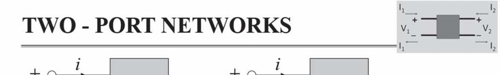


143


144


145


146
147


148

149

150
151


152

153


154


155


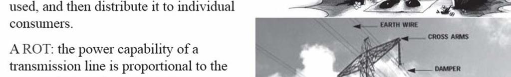


156

157


158
PROBLEMS. Figure13.74 For Prob Figure13.72 For Prob Figure13.75 For Prob Figure13.73 For Prob Figure13.76 For Prob
 CHAPTER 13 Magnetically Coupled Circuits 571 13.9 In order to match a source with internal impedance of 500 to a 15- load, what is needed is: (a) step-up linear transformer (b) step-down linear transformer
CHAPTER 9. Sinusoidal Steady-State Analysis
 CHAPTER 9 Sinusoidal Steady-State Analysis 9.1 The Sinusoidal Source A sinusoidal voltage source (independent or dependent) produces a voltage that varies sinusoidally with time. A sinusoidal current source
KINGS COLLEGE OF ENGINEERING DEPARTMENT OF ELECTRICAL AND ELECTRONICS ENGINEERING QUESTION BANK UNIT I BASIC CIRCUITS ANALYSIS PART A (2-MARKS)
") KINGS COLLEGE OF ENGINEERING DEPARTMENT OF ELECTRICAL AND ELECTRONICS ENGINEERING QUESTION BANK YEAR / SEM : I / II SUBJECT CODE & NAME : EE 1151 CIRCUIT THEORY UNIT I BASIC CIRCUITS ANALYSIS PART A (2-MARKS)
KINGS COLLEGE OF ENGINEERING DEPARTMENT OF ELECTRICAL AND ELECTRONICS ENGINEERING QUESTION BANK YEAR / SEM : I / II SUBJECT CODE & NAME : EE 1151 CIRCUIT THEORY UNIT I BASIC CIRCUITS ANALYSIS PART A (2-MARKS)
Questions Bank of Electrical Circuits
 Questions Bank of Electrical Circuits 1. If a 100 resistor and a 60 XL are in series with a 115V applied voltage, what is the circuit impedance? 2. A 50 XC and a 60 resistance are in series across a 110V
Question Paper Profile
 I Scheme Question Paper Profile Program Name : Electrical Engineering Program Group Program Code : EE/EP/EU Semester : Third Course Title : Electrical Circuits Max. Marks : 70 Time: 3 Hrs. Instructions:
VALLIAMMAI ENGINEERING COLLEGE
 P a g e 2 Question Bank Programme Subject Semester / Branch : BE : EE6201-CIRCUIT THEORY : II/EEE,ECE &EIE UNIT-I PART-A 1. Define Ohm s Law (B.L.T- 1) 2. List and define Kirchoff s Laws for electric circuits.
Downloaded from / 1
 PURWANCHAL UNIVERSITY II SEMESTER FINAL EXAMINATION-2008 LEVEL : B. E. (Computer/Electronics & Comm.) SUBJECT: BEG123EL, Electrical Engineering-I Full Marks: 80 TIME: 03:00 hrs Pass marks: 32 Candidates
AC Power Instructor Notes
 Chapter 7: AC Power Instructor Notes Chapter 7 surveys important aspects of electric power. Coverage of Chapter 7 can take place immediately following Chapter 4, or as part of a later course on energy
EE2003 Circuit Theory Chapter 13 Magnetically Coupled Circuits
 EE003 Circuit Theory Chapter 3 Magnetically Coupled Circuits Copyright The McGraw-Hill Companies, Inc. Permission required for reproduction or display. Magnetically Coupled Circuit Chapter 3 3. What is
Aligarh College of Engineering & Technology (College Code: 109) Affiliated to UPTU, Approved by AICTE Electrical Engg.
 Affiliated to UPTU, Approved by AICTE Electrical Engg.") Aligarh College of Engineering & Technology (College Code: 19) Electrical Engg. (EE-11/21) Unit-I DC Network Theory 1. Distinguish the following terms: (a) Active and passive elements (b) Linearity and
Aligarh College of Engineering & Technology (College Code: 19) Electrical Engg. (EE-11/21) Unit-I DC Network Theory 1. Distinguish the following terms: (a) Active and passive elements (b) Linearity and
EE 221 Circuits II. Chapter 13 Magnetically Coupled Circuits
 EE Circuits II Chapter 3 Magnetically Coupled Circuits Magnetically Coupled Circuits 3. What is a transformer? 3. Mutual Inductance 3.3 Energy in a Coupled Circuit 3.4 inear Transformers 3.5 Ideal Transformers
Review: Lecture 9. Instantaneous and Average Power. Effective or RMS Value. Apparent Power and Power Factor. Complex Power. Conservation of AC Power
 Review: Lecture 9 Instantaneous and Average Power p( t) VmI m cos ( v i ) VmI m cos ( t v i ) Maximum Average Power Transfer Z L R L jx Effective or RMS Value I rms I m L R P * TH Apparent Power and Power
SECTION 4 TRANSFORMERS. Yilu (Ellen) Liu. Associate Professor Electrical Engineering Department Virginia Tech University
 Liu. Associate Professor Electrical Engineering Department Virginia Tech University") SECTION 4 TRANSFORMERS Yilu (Ellen) Liu Associate Professor Electrical Engineering Department Virginia Tech University Analysis of Transformer Turns Ratio......................... 4.2 Analysis of a Step-Up
SECTION 4 TRANSFORMERS Yilu (Ellen) Liu Associate Professor Electrical Engineering Department Virginia Tech University Analysis of Transformer Turns Ratio......................... 4.2 Analysis of a Step-Up
EE6201 CIRCUIT THEORY QUESTION BANK PART A
 EE6201 CIRCUIT THEORY 1. State ohm s law. 2. State kirchoff s law. QUESTION BANK PART A 3. Which law is applicable for branch current method? 4. What is the matrix formation equation for mesh and nodal
Hours / 100 Marks Seat No.
 17323 14115 3 Hours / 100 Seat No. Instructions (1) All Questions are Compulsory. (2) Illustrate your answers with neat sketches wherever necessary. (3) Figures to the right indicate full marks. (4) Assume
CHAPTER 6: ALTERNATING CURRENT
 CHAPTER 6: ALTERNATING CURRENT PSPM II 2005/2006 NO. 12(C) 12. (c) An ac generator with rms voltage 240 V is connected to a RC circuit. The rms current in the circuit is 1.5 A and leads the voltage by
WALJAT COLLEGES OF APPLIED SCIENCES In academic partnership with BIRLA INSTITUTE OF TECHNOLOGY Question Bank Course: EC Session:
 WLJT OLLEGES OF PPLIED SIENES In academic partnership with IRL INSTITUTE OF TEHNOLOGY Question ank ourse: E Session: 20052006 Semester: II Subject: E2001 asic Electrical Engineering 1. For the resistive
Electrical Theory. Power Principles and Phase Angle. PJM State & Member Training Dept. PJM /22/2018
 Electrical Theory Power Principles and Phase Angle PJM State & Member Training Dept. PJM 2018 Objectives At the end of this presentation the learner will be able to: Identify the characteristics of Sine
86 chapter 2 Transformers
 86 chapter 2 Transformers Wb 1.2x10 3 0 1/60 2/60 3/60 4/60 5/60 6/60 t (sec) 1.2x10 3 FIGURE P2.2 2.3 A single-phase transformer has 800 turns on the primary winding and 400 turns on the secondary winding.
148 Electric Machines
 148 Electric Machines 3.1 The emf per turn for a single-phase 2200/220- V, 50-Hz transformer is approximately 12 V. Calculate (a) the number of primary and secondary turns, and (b) the net cross-sectional
Module 7. Transformer. Version 2 EE IIT, Kharagpur
 Module 7 Transformer Lesson 28 Problem solving on Transformers Contents 28 Problem solving on Transformer (Lesson-28) 4 28.1 Introduction. 4 28.2 Problems on 2 winding single phase transformers. 4 28.3
Chapter 2: Transformers
 Chapter 2: Transformers 2-1. The secondary winding of a transformer has a terminal voltage of v s (t) = 282.8 sin 377t V. The turns ratio of the transformer is 100:200 (a = 0.50). If the secondary current
SHRI RAMSWAROOP MEMORIAL COLLEGE OF ENGG. & MANAGEMENT B.Tech. [SEM I (EE, EN, EC, CE)] QUIZ TEST-3 (Session: ) Time: 1 Hour ELECTRICAL ENGINEE
![SHRI RAMSWAROOP MEMORIAL COLLEGE OF ENGG. & MANAGEMENT B.Tech. [SEM I (EE, EN, EC, CE)] QUIZ TEST-3 (Session: ) Time: 1 Hour ELECTRICAL ENGINEE](/thumbs/94/118213481.jpg "SHRI RAMSWAROOP MEMORIAL COLLEGE OF ENGG. & MANAGEMENT B.Tech. [SEM I (EE, EN, EC, CE)] QUIZ TEST-3 (Session: ) Time: 1 Hour ELECTRICAL ENGINEE") SHRI RAMSWAROOP MEMORIAL COLLEGE OF ENGG. & MANAGEMENT B.Tech. [SEM I (EE, EN, EC, CE)] QUIZ TEST-3 (Session: 2014-15) Time: 1 Hour ELECTRICAL ENGINEERING Max. Marks: 30 (NEE-101) Roll No. Academic/26
SHRI RAMSWAROOP MEMORIAL COLLEGE OF ENGG. & MANAGEMENT B.Tech. [SEM I (EE, EN, EC, CE)] QUIZ TEST-3 (Session: 2014-15) Time: 1 Hour ELECTRICAL ENGINEERING Max. Marks: 30 (NEE-101) Roll No. Academic/26
V.S.B ENGINEERING COLLEGE DEPARTMENT OF ELECTRICAL AND ELECTRONICS ENGINEERING I EEE-II Semester all subjects 2 & 16 marks QB
 V.S.B ENGINEERING COLLEGE DEPARTMENT OF ELECTRICAL AND ELECTRONICS ENGINEERING I EEE-II Semester all subjects 2 & 16 marks QB Sl.No Subject Name Page No. 1 Circuit Theory 2 1 UNIT-I CIRCUIT THEORY TWO
I. Introduction to Simple Circuits of Resistors
 2 Problem Set for Dr. Todd Huffman Michaelmas Term I. Introduction to Simple ircuits of esistors 1. For the following circuit calculate the currents through and voltage drops across all resistors. The
SIDDHARTH GROUP OF INSTITUTIONS :: PUTTUR (AUTONOMOUS) Siddharth Nagar, Narayanavanam Road QUESTION BANK (DESCRIPTIVE) UNIT I INTRODUCTION
 Siddharth Nagar, Narayanavanam Road QUESTION BANK (DESCRIPTIVE) UNIT I INTRODUCTION") SIDDHARTH GROUP OF INSTITUTIONS :: PUTTUR (AUTONOMOUS) Siddharth Nagar, Narayanavanam Road 517583 QUESTION BANK (DESCRIPTIVE) Subject with Code : Electrical Circuits(16EE201) Year & Sem: I-B.Tech & II-Sem
SIDDHARTH GROUP OF INSTITUTIONS :: PUTTUR (AUTONOMOUS) Siddharth Nagar, Narayanavanam Road 517583 QUESTION BANK (DESCRIPTIVE) Subject with Code : Electrical Circuits(16EE201) Year & Sem: I-B.Tech & II-Sem
Class XII Chapter 7 Alternating Current Physics
 Question 7.1: A 100 Ω resistor is connected to a 220 V, 50 Hz ac supply. (a) What is the rms value of current in the circuit? (b) What is the net power consumed over a full cycle? Resistance of the resistor,
ELECTROMAGNETIC INDUCTION AND ALTERNATING CURRENT (Assignment)
") ELECTROMAGNETIC INDUCTION AND ALTERNATING CURRENT (Assignment) 1. In an A.C. circuit A ; the current leads the voltage by 30 0 and in circuit B, the current lags behind the voltage by 30 0. What is the
ELECTROMAGNETIC INDUCTION AND ALTERNATING CURRENT (Assignment) 1. In an A.C. circuit A ; the current leads the voltage by 30 0 and in circuit B, the current lags behind the voltage by 30 0. What is the
ECE 2006 University of Minnesota Duluth Lab 11. AC Circuits
 1. Objective AC Circuits In this lab, the student will study sinusoidal voltages and currents in order to understand frequency, period, effective value, instantaneous power and average power. Also, the
Look over Chapter 31 sections 1-4, 6, 8, 9, 10, 11 Examples 1-8. Look over Chapter 21 sections Examples PHYS 2212 PHYS 1112
 PHYS 2212 Look over Chapter 31 sections 1-4, 6, 8, 9, 10, 11 Examples 1-8 PHYS 1112 Look over Chapter 21 sections 11-14 Examples 16-18 Good Things To Know 1) How AC generators work. 2) How to find the
ELECTRIC CIRCUITS. Third Edition JOSEPH EDMINISTER MAHMOOD NAHVI
 ELECTRIC CIRCUITS Third Edition JOSEPH EDMINISTER MAHMOOD NAHVI Includes 364 solved problems --fully explained Complete coverage of the fundamental, core concepts of electric circuits All-new chapters
ELEN 140 ELECTRICAL CIRCUITS II Winter 2013
 ELEN 140 ELECTRICAL CIRCUITS II Winter 2013 Professor: Stephen O Loughlin Prerequisite: ELEN 130 Office: C234B Co-requisite: none Office Ph: (250) 762-5445 ext 4376 Lecture: 3.0 hrs/week Email: soloughlin@okanagan.bc.ca
CHAPTER 11. Balanced Three-Phase Circuits
 CHAPTER 11 Balanced Three-Phase Circuits 11.1 Balanced Three-Phase Voltages Three sinusoidal voltages Identical amplitudes and frequencies Out of phase 120 with each other by exactly As the a-phase voltage,
TRANSFORMER OPERATION
 Chapter 3 TRANSFORMER OPERATION 1 A transformer is a static device (no moving parts) used to transfer energy from one AC circuit to another. This transfer of energy may involve an increase or decrease
Chapter 2. The Fundamentals of Electronics: A Review
 Chapter 2 The Fundamentals of Electronics: A Review Topics Covered 2-1: Gain, Attenuation, and Decibels 2-2: Tuned Circuits 2-3: Filters 2-4: Fourier Theory 2-1: Gain, Attenuation, and Decibels Most circuits
RLC Frequency Response
 1. Introduction RLC Frequency Response The student will analyze the frequency response of an RLC circuit excited by a sinusoid. Amplitude and phase shift of circuit components will be analyzed at different
Chapter 7. Copyright The McGraw-Hill Companies, Inc. Permission required for reproduction or display.
 Chapter 7 Copyright The McGraw-Hill Companies, Inc. Permission required for reproduction or display. Learning Objectives 1. Understand the meaning of instantaneous and average power, master AC power notation,
Module 1. Introduction. Version 2 EE IIT, Kharagpur
 Module 1 Introduction Lesson 1 Introducing the Course on Basic Electrical Contents 1 Introducing the course (Lesson-1) 4 Introduction... 4 Module-1 Introduction... 4 Module-2 D.C. circuits.. 4 Module-3
ET1210: Module 5 Inductance and Resonance
 Part 1 Inductors Theory: When current flows through a coil of wire, a magnetic field is created around the wire. This electromagnetic field accompanies any moving electric charge and is proportional to
Spring 2000 EE361: MIDTERM EXAM 1
 NAME: STUDENT NUMBER: Spring 2000 EE361: MIDTERM EXAM 1 This exam is open book and closed notes. Assume f=60 hz and use the constant µ o =4π 10-7 wherever necessary. Be sure to show all work clearly. 1.
Chapter 33. Alternating Current Circuits
 Chapter 33 Alternating Current Circuits Alternating Current Circuits Electrical appliances in the house use alternating current (AC) circuits. If an AC source applies an alternating voltage to a series
13. Magnetically Coupled Circuits
 13. Magnetically Coupled Circuits The change in the current flowing through an inductor induces (creates) a voltage in the conductor itself (self-inductance) and in any nearby conductors (mutual inductance)
Downloaded From All JNTU World
 Code: 9A02403 GENERATION OF ELECTRIC POWER 1 Discuss the advantages and disadvantages of a nuclear plant as compared to other conventional power plants. 2 Explain about: (a) Solar distillation. (b) Solar
Physics for Scientists & Engineers 2 2 = 1 LC. Review ( ) Review (2) Review (3) e! Rt. cos "t + # ( ) q = q max. Spring Semester 2005 Lecture 30 U E
 Review (2) Review (3) e! Rt. cos t + # ( ) q = q max. Spring Semester 2005 Lecture 30 U E") Review hysics for Scientists & Engineers Spring Semester 005 Lecture 30! If we have a single loop RLC circuit, the charge in the circuit as a function of time is given by! Where q = q max e! Rt L cos "t
Review hysics for Scientists & Engineers Spring Semester 005 Lecture 30! If we have a single loop RLC circuit, the charge in the circuit as a function of time is given by! Where q = q max e! Rt L cos "t
Figure Derive the transient response of RLC series circuit with sinusoidal input. [15]
![Figure Derive the transient response of RLC series circuit with sinusoidal input. [15]](/thumbs/84/91046828.jpg "Figure Derive the transient response of RLC series circuit with sinusoidal input. [15]") COURTESY IARE Code No: R09220205 R09 SET-1 B.Tech II Year - II Semester Examinations, December-2011 / January-2012 NETWORK THEORY (ELECTRICAL AND ELECTRONICS ENGINEERING) Time: 3 hours Max. Marks: 80 Answer
COURTESY IARE Code No: R09220205 R09 SET-1 B.Tech II Year - II Semester Examinations, December-2011 / January-2012 NETWORK THEORY (ELECTRICAL AND ELECTRONICS ENGINEERING) Time: 3 hours Max. Marks: 80 Answer
ECE 201 LAB 8 TRANSFORMERS & SINUSOIDAL STEADY STATE ANALYSIS
 Version 1.1 1 of 8 ECE 201 LAB 8 TRANSFORMERS & SINUSOIDAL STEADY STATE ANALYSIS BEFORE YOU BEGIN PREREQUISITE LABS Introduction to MATLAB Introduction to Lab Equipment Introduction to Oscilloscope Capacitors,
Transformers 21.1 INTRODUCTION 21.2 MUTUAL INDUCTANCE
 21 Transformers 21.1 INTRODUCTION Chapter 12 discussed the self-inductance of a coil. We shall now examine the mutual inductance that exists between coils of the same or different dimensions. Mutual inductance
University of Jordan School of Engineering Electrical Engineering Department. EE 219 Electrical Circuits Lab
 University of Jordan School of Engineering Electrical Engineering Department EE 219 Electrical Circuits Lab EXPERIMENT 7 RESONANCE Prepared by: Dr. Mohammed Hawa EXPERIMENT 7 RESONANCE OBJECTIVE This experiment
VETRI VINAYAHA COLLEGE OF ENGINEERING AND TECHNOLOGY
 VETRI VINAYAHA COLLEGE OF ENGINEERING AND TECHNOLOGY DEPARTMENT OF ELECTRICAL AND ELECTRONICS ENGINEERING I-YEAR/II-SEMESTER- EEE&ECE EE6201- CIRCUIT THEORY Two Marks with Answers PREPARED BY: Mr.A.Thirukkumaran,
BEST BMET CBET STUDY GUIDE MODULE ONE
 BEST BMET CBET STUDY GUIDE MODULE ONE 1 OCTOBER, 2008 1. The phase relation for pure capacitance is a. current leads voltage by 90 degrees b. current leads voltage by 180 degrees c. current lags voltage
Electric Circuits II Magnetically Coupled Circuits. Dr. Firas Obeidat
 Electric Circuits II Magnetically Coupled Circuits Dr. Firas Obeidat 1 Table of contents 1 Mutual Inductance 2 Dot Convention 3 Analyze Circuits Involving Mutual Inductance 4 Energy in a Coupled Circuit
B.Tech II SEM Question Bank. Electronics & Electrical Engg UNIT-1
 UNIT-1 1. State & Explain Superposition theorem & Thevinin theorem with example? 2. Calculate the current in the 400Ωm resistor of below figure by Superposition theorem. 3. State & Explain node voltage
PART B. t (sec) Figure 1
 Figure 1") Code No: R16128 R16 SET 1 I B. Tech II Semester Regular Examinations, April/May 217 ELECTRICAL CIRCUIT ANALYSIS I (Electrical and Electronics Engineering) Time: 3 hours Max. Marks: 7 Note: 1. Question
Code No: R16128 R16 SET 1 I B. Tech II Semester Regular Examinations, April/May 217 ELECTRICAL CIRCUIT ANALYSIS I (Electrical and Electronics Engineering) Time: 3 hours Max. Marks: 7 Note: 1. Question
Electric Circuits II Three-Phase Circuits. Dr. Firas Obeidat
 Electric Circuits II Three-Phase Circuits Dr. Firas Obeidat 1 Table of Contents 1 Balanced Three-Phase Voltages 2 Balanced Wye-Wye Connection 3 Balanced Wye-Delta Connection 4 Balanced Delta-Delta Connection
AC reactive circuit calculations
 AC reactive circuit calculations This worksheet and all related files are licensed under the Creative Commons Attribution License, version 1.0. To view a copy of this license, visit http://creativecommons.org/licenses/by/1.0/,
Exercise 9: inductor-resistor-capacitor (LRC) circuits
 circuits") Exercise 9: inductor-resistor-capacitor (LRC) circuits Purpose: to study the relationship of the phase and resonance on capacitor and inductor reactance in a circuit driven by an AC signal. Introduction
Exercise 9: inductor-resistor-capacitor (LRC) circuits Purpose: to study the relationship of the phase and resonance on capacitor and inductor reactance in a circuit driven by an AC signal. Introduction
Lecture 16 Date: Frequency Response (Contd.)
") Lecture 16 Date: 03.10.2017 Frequency Response (Contd.) Bode Plot (contd.) Bode Plot (contd.) Bode Plot (contd.) not every transfer function has all seven factors. To sketch the Bode plots for a generic
Lecture 16 Date: 03.10.2017 Frequency Response (Contd.) Bode Plot (contd.) Bode Plot (contd.) Bode Plot (contd.) not every transfer function has all seven factors. To sketch the Bode plots for a generic
Chapter 16: Mutual Inductance
 Chapter 16: Mutual Inductance Instructor: Jean-François MILLITHALER http://faculty.uml.edu/jeanfrancois_millithaler/funelec/spring2017 Slide 1 Mutual Inductance When two coils are placed close to each
Chapter 11. Alternating Current
 Unit-2 ECE131 BEEE Chapter 11 Alternating Current Objectives After completing this chapter, you will be able to: Describe how an AC voltage is produced with an AC generator (alternator) Define alternation,
TRANSFORMER THEORY. Mutual Induction
 Transformers Transformers are used extensively for AC power transmissions and for various control and indication circuits. Knowledge of the basic theory of how these components operate is necessary to
Designing Information Devices and Systems II Fall 2018 Elad Alon and Miki Lustig Homework 4
 EECS 16B Designing Information Devices and Systems II Fall 2018 Elad Alon and Miki Lustig Homework 4 This homework is solely for your own practice. However, everything on it is in scope for midterm 1,
15. the power factor of an a.c circuit is.5 what will be the phase difference between voltage and current in this
 1 1. In a series LCR circuit the voltage across inductor, a capacitor and a resistor are 30 V, 30 V and 60 V respectively. What is the phase difference between applied voltage and current in the circuit?
CHAPTER 2. Transformers. Dr Gamal Sowilam
 CHAPTER Transformers Dr Gamal Sowilam Introduction A transformer is a static machine. It is not an energy conversion device, it is indispensable in many energy conversion systems. A transformer essentially
Circuit Systems with MATLAB and PSpice
 Circuit Systems with MATLAB and PSpice Won Y. Yang and Seung C. Lee Chung-Ang University, South Korea BICENTENNIAL 9 I CE NTE NNIAL John Wiley & Sons(Asia) Pte Ltd Contents Preface Limits of Liability
Reg. No. : BASIC ELECTRICAL TECHNOLOGY (ELE 101)
") Department of Electrical and Electronics Engineering Reg. No. : MNIPL INSTITUTE OF TECHNOLOGY, MNIPL ( Constituent Institute of Manipal University, Manipal) FIRST SEMESTER B.E. DEGREE MKEUP EXMINTION (REVISED
Department of Electrical and Electronics Engineering Reg. No. : MNIPL INSTITUTE OF TECHNOLOGY, MNIPL ( Constituent Institute of Manipal University, Manipal) FIRST SEMESTER B.E. DEGREE MKEUP EXMINTION (REVISED
Downloaded From JNTU World. B.Tech II Year II Semester (R09) Supplementary Examinations December/January 2014/2015 GENERATION OF ELECTRIC POWER
 Supplementary Examinations December/January 2014/2015 GENERATION OF ELECTRIC POWER") Downloaded From Code: 9A02403 B.Tech II Year II Semester () Supplementary Examinations December/January 2014/2015 GENERATION OF ELECTRIC POWER Answer any FIVE questions 1 Discuss the advantages and disadvantages
Downloaded From Code: 9A02403 B.Tech II Year II Semester () Supplementary Examinations December/January 2014/2015 GENERATION OF ELECTRIC POWER Answer any FIVE questions 1 Discuss the advantages and disadvantages
Department of Electrical & Computer Engineering Technology. EET 3086C Circuit Analysis Laboratory Experiments. Masood Ejaz
 Department of Electrical & Computer Engineering Technology EET 3086C Circuit Analysis Laboratory Experiments Masood Ejaz Experiment # 1 DC Measurements of a Resistive Circuit and Proof of Thevenin Theorem
Electrical Engineering Fundamentals
 Electrical Engineering Fundamentals EE-238 Sheet 1 Series Circuits 1- For the circuits shown below, the total resistance is specified. Find the unknown resistance and the current for each circuit. 12.6
CHAPTER 2. Basic Concepts, Three-Phase Review, and Per Unit
 CHAPTER 2 Basic Concepts, Three-Phase Review, and Per Unit 1 AC power versus DC power DC system: - Power delivered to the load does not fluctuate. - If the transmission line is long power is lost in the
Sirindhorn International Institute of Technology Thammasat University
 Sirindhorn International Institute of Technology Thammasat University School of Information, Computer and Communication Technology COURSE : ECS 34 Basic Electrical Engineering Lab INSTRUCTOR : Dr. Prapun
Kerwin, W.J. Passive Signal Processing The Electrical Engineering Handbook Ed. Richard C. Dorf Boca Raton: CRC Press LLC, 2000
 Kerwin, W.J. Passive Signal Processing The Electrical Engineering Handbook Ed. Richard C. Dorf Boca Raton: CRC Press LLC, 000 4 Passive Signal Processing William J. Kerwin University of Arizona 4. Introduction
ECE 215 Lecture 8 Date:
 ECE 215 Lecture 8 Date: 28.08.2017 Phase Shifter, AC bridge AC Circuits: Steady State Analysis Phase Shifter the circuit current I leads the applied voltage by some phase angle θ, where 0 < θ < 90 ο depending
Lecture 4 - Three-phase circuits, transformer and transient analysis of RLC circuits. Figure 4.1
 Lecture 4 - Three-phase circuits, transformer and transient analysis of RLC circuits Power supply to sizeable power converters are often from three-phase AC source. A balanced three-phase source consists
EE233 Autumn 2016 Electrical Engineering University of Washington. EE233 HW7 Solution. Nov. 16 th. Due Date: Nov. 23 rd
 EE233 HW7 Solution Nov. 16 th Due Date: Nov. 23 rd 1. Use a 500nF capacitor to design a low pass passive filter with a cutoff frequency of 50 krad/s. (a) Specify the cutoff frequency in hertz. fc c 50000
Unit-1(A) Circuit Analysis Techniques
 Circuit Analysis Techniques") Unit-1(A Circuit Analysis Techniques Basic Terms used in a Circuit 1. Node :- It is a point in a circuit where two or more circuit elements are connected together. 2. Branch :- It is that part of a network
Unit-1(A Circuit Analysis Techniques Basic Terms used in a Circuit 1. Node :- It is a point in a circuit where two or more circuit elements are connected together. 2. Branch :- It is that part of a network
An induced emf is the negative of a changing magnetic field. Similarly, a self-induced emf would be found by
 This is a study guide for Exam 4. You are expected to understand and be able to answer mathematical questions on the following topics. Chapter 32 Self-Induction and Induction While a battery creates an
Lecture # 3 Circuit Configurations
 CPEN 206 Linear Circuits Lecture # 3 Circuit Configurations Dr. Godfrey A. Mills Email: gmills@ug.edu.gh Phone: 0269073163 February 15, 2016 Course TA David S. Tamakloe CPEN 206 Lecture 3 2015_2016 1 Circuit
Chapter 13 Magnetically Coupled Circuits. Chapter Objectives:
 Chapter 13 Magnetically Coupled Circuits Chapter Objectives: Understand magnetically coupled circuits. Learn the concept of mutual inductance. Be able to determine energy in a coupled circuit. Learn how
UNIT 1 CIRCUIT ANALYSIS 1 What is a graph of a network? When all the elements in a network is replaced by lines with circles or dots at both ends.
 UNIT 1 CIRCUIT ANALYSIS 1 What is a graph of a network? When all the elements in a network is replaced by lines with circles or dots at both ends. 2 What is tree of a network? It is an interconnected open
Lecture # 4 Network Analysis
 CPEN 206 Linear Circuits Lecture # 4 Network Analysis Dr. Godfrey A. Mills Email: gmills@ug.edu.gh Phone: 026-907-3163 February 22, 2016 Course TA David S. Tamakloe 1 What is Network Technique o Network
Experiment 45. Three-Phase Circuits. G 1. a. Using your Power Supply and AC Voltmeter connect the circuit shown OBJECTIVE
 Experiment 45 Three-Phase Circuits OBJECTIVE To study the relationship between voltage and current in three-phase circuits. To learn how to make delta and wye connections. To calculate the power in three-phase
FREQUENCY RESPONSE AND PASSIVE FILTERS LABORATORY
 FREQUENCY RESPONSE AND PASSIVE FILTERS LABORATORY In this experiment we will analytically determine and measure the frequency response of networks containing resistors, AC source/sources, and energy storage
Cork Institute of Technology. Autumn 2008 Electrical Energy Systems (Time: 3 Hours)
") Cork Institute of Technology Bachelor of Science (Honours) in Electrical Power Systems - Award Instructions Answer FIVE questions. (EELPS_8_Y4) Autumn 2008 Electrical Energy Systems (Time: 3 Hours) Examiners:
Cork Institute of Technology Bachelor of Science (Honours) in Electrical Power Systems - Award Instructions Answer FIVE questions. (EELPS_8_Y4) Autumn 2008 Electrical Energy Systems (Time: 3 Hours) Examiners:
Lab 1: Basic RL and RC DC Circuits
 Name- Surname: ID: Department: Lab 1: Basic RL and RC DC Circuits Objective In this exercise, the DC steady state response of simple RL and RC circuits is examined. The transient behavior of RC circuits
Chapter 6: Alternating Current
 hapter 6: Alternating urrent 6. Alternating urrent.o 6.. Define alternating current (A) An alternating current (A) is the electrical current which varies periodically with time in direction and magnitude.
CHAPTER 7. Response of First-Order RL and RC Circuits
 CHAPTER 7 Response of First-Order RL and RC Circuits RL and RC Circuits RL (resistor inductor) and RC (resistor-capacitor) circuits. Figure 7.1 The two forms of the circuits for natural response. (a) RL
ECE2210 Final given: Fall 12
 ECE Final given: Fall (5 pts) a) Find and draw the Thévenin equivalent of the circuit shown The load resistor is R L b) Find and draw the Norton equivalent of the same circuit c) Find the load current
El-Hawary, M.E. The Transformer Electrical Energy Systems. Series Ed. Leo Grigsby Boca Raton: CRC Press LLC, 2000
 El-Hawary, M.E. The Transformer Electrical Energy Systems. Series Ed. Leo Grigsby Boca Raton: CRC Press LLC, 000 97 Chapter 4 THE TRANSFORMER 4. NTRODUCTON The transformer is a valuable apparatus in electrical
ENGINEERING CIRCUIT ANALYSIS
 ENGINEERING CIRCUIT ANALYSIS EIGHTH EDITION William H. Hayt, Jr. (deceased) Purdue University Jack E. Kemmerly (deceased) California State University Steven M. Durbin University at Buffalo The State University
Designing Information Devices and Systems II Fall 2018 Elad Alon and Miki Lustig Homework 4
 EECS 6B Designing Information Devices and Systems II Fall 208 Elad Alon and Miki Lustig Homework 4 This homework is solely for your own practice. However, everything on it is in scope for midterm, and
GRADE 12 SEPTEMBER 2012 ELECTRICAL TECHNOLOGY
 Province of the EASTERN CAPE EDUCATION NATIONAL SENIOR CERTIFICATE GRADE 12 SEPTEMBER 2012 ELECTRICAL TECHNOLOGY MARKS: 200 TIME: 3 hours This question paper consists of 11 pages and a formula sheet. 2
Paper-1 (Circuit Analysis) UNIT-I
 UNIT-I") Paper-1 (Circuit Analysis) UNIT-I AC Fundamentals & Kirchhoff s Current and Voltage Laws 1. Explain how a sinusoidal signal can be generated and give the significance of each term in the equation? 2. Define
Paper-1 (Circuit Analysis) UNIT-I AC Fundamentals & Kirchhoff s Current and Voltage Laws 1. Explain how a sinusoidal signal can be generated and give the significance of each term in the equation? 2. Define
CHAPTER 4 FULL WAVE RECTIFIER. AC DC Conversion
 CHAPTER 4 FULL WAVE RECTIFIER AC DC Conversion SINGLE PHASE FULL-WAVE RECTIFIER The objective of a full wave rectifier is to produce a voltage or current which is purely dc or has some specified dc component.
EE12: Laboratory Project (Part-2) AM Transmitter
 AM Transmitter") EE12: Laboratory Project (Part-2) AM Transmitter ECE Department, Tufts University Spring 2008 1 Objective This laboratory exercise is the second part of the EE12 project of building an AM transmitter in
EE12: Laboratory Project (Part-2) AM Transmitter ECE Department, Tufts University Spring 2008 1 Objective This laboratory exercise is the second part of the EE12 project of building an AM transmitter in
AC : A CIRCUITS COURSE FOR MECHATRONICS ENGINEERING
 AC 2010-2256: A CIRCUITS COURSE FOR MECHATRONICS ENGINEERING L. Brent Jenkins, Southern Polytechnic State University American Society for Engineering Education, 2010 Page 15.14.1 A Circuits Course for
EE-2302 Passive Filters and Frequency Response
 EE2302 Passive Filters and Frequency esponse Objective he student should become acquainted with simple passive filters for performing highpass, lowpass, and bandpass operations. he experimental tasks also
Electromagnetic Oscillations and Currents. March 23, 2014 Chapter 30 1
 Electromagnetic Oscillations and Currents March 23, 2014 Chapter 30 1 Driven LC Circuit! The voltage V can be thought of as the projection of the vertical axis of the phasor V m representing the time-varying
UNIVERSITY OF BOLTON SCHOOL OF SPORT AND BIOMEDICAL SCIENCE. BEng (HONS)/MEng BIOMEDICAL ENGINEERING. BEng (HONS) MEDICAL ENGINEERING
/MEng BIOMEDICAL ENGINEERING. BEng (HONS) MEDICAL ENGINEERING") LH29 SCHOOL OF SPORT AND BIOMEDICAL SCIENCE BEng (HONS)/MEng BIOMEDICAL ENGINEERING BEng (HONS) MEDICAL ENGINEERING SEMESTER 2 EXAMINATIONS 2015/2016 MODULE NO: BME4004 Date: Wednesday 18 May 2016 Time:
LH29 SCHOOL OF SPORT AND BIOMEDICAL SCIENCE BEng (HONS)/MEng BIOMEDICAL ENGINEERING BEng (HONS) MEDICAL ENGINEERING SEMESTER 2 EXAMINATIONS 2015/2016 MODULE NO: BME4004 Date: Wednesday 18 May 2016 Time:
Instructions for the final examination:
 School of Information, Computer and Communication Technology Sirindhorn International Institute of Technology Thammasat University Practice Problems for the Final Examination COURSE : ECS304 Basic Electrical
Introduction... 1 Part I: Getting Started with Circuit Analysis Part II: Applying Analytical Methods for Complex Circuits...
 Contents at a Glance Introduction... 1 Part I: Getting Started with Circuit Analysis... 5 Chapter 1: Introducing Circuit Analysis...7 Chapter 2: Clarifying Basic Circuit Concepts and Diagrams...15 Chapter