ECE 8700, Communication Systems Engineering, Spring 2011 Course Information (Draft: 12/29/10)
|
|
|
- Gary Hodges
- 5 years ago
- Views:
Transcription
1 ECE 8700, Communication Systems Engineering, Spring 20 Course Information (Draft: 2/29/0) Instructor: Kevin Buckley, Tolentine 433a, (Office), (Fax), (CEER307), Office Hours: * Mon. :30am-2:30pm(T433a); Wed. :30am-2:30pm(T433a); Thurs. -2pm(T433a); Fri. 9:30-0:30am (T433a) * by appointment, or stop in any time I m available Prerequisites: Undergraduate background in engineering probability and statistics, and in principles of communications (equivalent to ECE 3720 and ECE 3770). Grading Policy: * Homework: due before class about every other week - 20% * Three Computer Assignments - 0% each * Test : Wed. 2/23 (Chapts. -3 of Course Notes), 2 hrs. in class - 25 % * Test 2: Finals Week (Chapts. 4-7 of Course Notes), 2 hrs. in class - 25 % Text: Digital Communications, 5-th edition, by John Proakis & Masoud Salehi, McGraw- Hill, ISBN: Course Notes will be provided. Primarily, you will be responsible for the material in the Course Notes. The Text will be used extensively as a reference, so you will be responsible for specific Sections of the Text which will be identified. Reference: Introduction to Analog and Digital Communications, 2-nd edition, by Simon Haykin & Michael Moher, Wiley & Sons, Signals & Systems 2-nd ed., Alan Oppenheim & Alan Willsky, Prentice-Hall, 997. Linear Algebra and Its Applications, 3-rd ed., by Gilbert Strang, Harcourt Brace Jovanovich, 976. Probability, Random Variables, and Random Signal Principles, 4-th ed., by Payton Peebles, McGraw Hill, 200. Course Description: This course covers basic topics in digital communications. Topics covered in-depth include: modulation schemes, maximum likelihood detection, maximum likelihood sequence estimation, the Viterbi algorithm, carrier and symbol synchronization, bandlimited channels, intersymbol interference modeling, and optimum channel equalization. We also briefly overview: adaptive equalization; information theory & coding; fading channels, MIMO systems and space-time coding; multicarrier and spread spectrum communications; and multiuser communications.
2 ECE 8700, Communication Systems Engineering, Spring 200 Homework, Computer Assignment & Text Policies Submission of Homeworks (HWs) & Computer Assignments (CAs): Distance education students can submit HWs and CAs by Fax ( ) or For Fax submissions, only one transmission is accepted per assignment. For s, only one file will be accepted per assignment, and that file can be only a.pdf or.doc file (e.g. not.zip or.docx files). Assignments are due by the beginning of class on the date indicated on the assignment (i.e. on a Wednesday), however they will not be considered late if submitted by midnight that day. If submitted between midnight and 5pm the next day (Thursday), 0% will be deducted for being late. If submitted between 5pm Thursday and noon that Friday, 20% will be deducted for being late. If submitted after noon on that Friday (the solutions will be posted at noon on Fridays), at least 40% will be deducted for being late. Each student must do each problem to be submitted without interaction with others. Students are encouraged to work with others in understanding and solving the Homework Set problems which are not required to be submitted. In-class students can submit assignments either in class or in my mailbox before class. They can also submit by or Fax. The late submission policy is the same as for distance education students (as identified above). Distance Education Student Test Policies: Any distance education student is welcome and even encouraged to take the test in class. However, realizing that this in not practical for everyone, the following distance education testing procedure will be available. Test dates are listed on the Course Information Page. On the afternoon of a test, there will a roughly half hour lecture to begin with, followed by a 0 minute break, followed by the test till 6pm. The test will be made available, as a.pdf file on the Course Homework page, at the beginning of the 0 minute break. The test is to be completed by 6pm. The test work must be submitted by Fax ( ) or (as a scanned.pdf or.doc file) by 6:05pm. 2
3 ECE 8700, Communication Systems Engineering, Spring 20 Course Outline Part : Introduction to Digital Communications (Chapters -3; Lectures -4) [ ] Background. Digital communication system block diagram & Course focus.2 Bandpass signals and systems.2. Review of the Continuous-Time Fourier Transform (CTFT).2.2 Real-valued bandpass (narrowband) signals & lowpass equivalents.2.3 Real-valued Linear Time-Invariant (LTI) bandpass systems.3 Representation of digital communication signals.3. Linear space concepts.3.2 Linear space representation of digital communication symbols.3.3 Discrete-Time (DT) signals and the DT Fourier Transform (DTFT).3.4 DT information signals.4 Selected review of probability and random processes: probability, random variables, statistical independence, expectation & moments, Gaussian & other random variables, probability bounds, weighted sums of multiple random variables, random processes [2 ] Representation of digitally modulated signals 2. Pulse amplitude modulation (PAM) 2.2 Phase modulation (e.g. PSK) 2.3 Quadrature amplitude modulation (QAM) 2.4 Notes on multidimensional modulation schemes (e.g. FSK) 2.5 Several modulation schemes with memory: DPSK, PRS, CPM 2.6 Spectral characteristics of digitally modulated signals
4 Part 2: Symbol Detection & Sequence Estimation (Chapters 4-5; Lectures 5-9) [3 ] Symbol Detection 3. Correlation receiver & matched filter for symbol detection 3.. Correlation receiver 3..2 Matched filter 3..3 Nearest neighbor detection 3.2 Optimum symbol detector 3.2. Maximum likelihood (ML) detector Maximum a posterior (MAP) detector 3.3 Performance of linear, memoryless modulation schemes: binary PSK, orthogonal modulation, PSK, PAM, QAM, FSK; examples & bandwidth considerations 3.4 Decoding DPSK - a suboptimum symbol detector [4 ] Maximum likelihood sequence estimation (MLSE) 4. Noninteracting symbols 4.2 MLSE for DPSK 4.3 MLSE for Partial Response Signaling (PRS) 4.4 MLSE for CPM 4.5 The Viterbi algorithm 4.6 Symbol-by-symbol MAP and the BCJR algorithm 4.7 A comparison between MLSE/Viterbi and MAP/BCJR [5 ] Noncoherent Detection & Synchronization 5. Reception with carrier phase & symbol timing uncertainty 5.2 Noncoherent detection 5.3 From ML/MAP detection to ML/MAP parameter estimation 5.4 Carrier phase estimation 5.5 Symbol timing estimation 5.6 Joint carrier phase & symbol timing estimation 2
5 Part 3: Bandlimited & InterSymbol Interference (ISI) Channels (Chapters 9-0; Lectures 0-3) [6 ] Bandlimited channels & intersymbol interference 6. The digital communication channel & ISI 6.2 Signal design (e.g. PRS) for bandlimited channels 6.3 A DT ISI channel model 6.4 MLSE and the Viterbi algorithm for ISI channels [7 ] Channel Equalization 7. Basis concepts 7.2 Linear Equalization 7.2. Channel inversion Mean Square Error (MSE) criterion Additional linear MMSE equalizer issues 7.3 Decision feedback equalization 7.4 Adaptive Equalization 7.5 Alternative adaptation schemes 7.6 MLSE with unknown channels Part 4: Overview of Advanced Digital Communications Topics (Selected topics from Chapters -3, 5-6; Lecture 4) [8 ] Overview of Information Theory and Coding [9 ] Overview of Space-Time Coding & Multiple-Input Multiple-Output (MIMO) Systems [0 ] Spread Spectrum & Multiuser Communications 3
6 ECE 8700 Communication System Engineering, Spring 20 Homework Set # Suggested Problems from the Text 2.,2.2,2.7,2.9 (signal & system theory for digital communications) Homework # (Due Wed., Jan. 9 before class): (Do all. Submit problems 3, 4, 5, 6, 7.). Problem 2.2 of the Course Text. 2. Problem 2.9 of the Course Text. 3. A symbol g(t) = p 0 (t 5) is transmitted through a CT LTI channel with impulse response c(t) = p 0 (t). Determine the output y(t) and it CTFT Y(f). 4. Consider x(t) = 0 cos(2π300t) and modulation frequency f c = 00,000 Hz. Determine x + (t), X + (f), x l (t) and X l (f). 5. Consider a lowpass equivalent signal x l (t) with CTFT X l (f) = Λ ( ) f 00 e j20πf (see the notation on p. 7 of the Course Text). Determine X + (f) and X(f). Determine x(t). Determine the energy of x(t), x + (t) and x l (t). 6. Consider s(t) = g(t) cos(2π000t), where g(t) = 0 sinc(0t) (see the notation on p. 7 of the Course Text). Let r(t) = A s(t τ o ). Say that r(t) is demodulated to form r l (t), using the demodulator in Figure 2 of the Course Notes where the demodulation frequency is f c = 990 Hz. Determine G(f), S(f), R(f) and R l (f). 7. Considerabandpasschannelwithlowpassequivalentimpulseresponseh l (t) = sinc 2 (00πt) which has frequency response centered around f c = 000 Hz. The channel input is x(t) = 2 cos(00πt) + 3 cos(950πt) + 4 cos(000πt). Determine the channel output y(t), it complex analytic representation y + (t), and its lowpass equivalent y l (t). 8. Consider the set of signals {x k (t) = sinc(t k); k = 0,±,±2, }. Show that they forman orthonormal set (i.e. show that the inner product x i(t) x j (t) dt = δ[i j] where δ[k] is the discrete impulse function). (Hints: the sinc function is define on p. 7 of the Course Text. Use the CTFT representations of the x k (t) when evaluating the inner products. Use Table on p. 9 of the Course Text and the delay property in Table 2.0- for x k (t) the CTFT. Use the following fact from generalized functions, e j2πft dt = δ(f) () where δ(f) is the continuous impulse function.)
7 ECE 8700 Communication System Engineering, Spring 20 Homework Set # 2 Suggested Problems from the Text 2.3,2.6,2.8,2.,2.2,2.3 (signal space representation) 2.3-4, 2.6 (probability); 2.5, (random variables) Homework # 2 (Due Wed., Jan. 26 before class): (Do all. Submit problems 2,4,5,6,9.). Low rank representation of vectors: (a) In Lecture 2-3 Course Notes, after Eq (0), it is noted that the coefficients s k = v H k v minimize the Euclidean norm (i.e. the energy) of the error vector m e = v ˆv = v s k v k = v V s k= of the the low rank orthonormal expansion of n-dimensional vector v with respect to the orthonormal vectors v k ; k =,2,,m (where m < n). Prove this by taking the derivatives of e 2 with respect to the s k ; k =,2,,m and setting them equal to zero. To simplify this, assume all values are real-valued. (b) Given the optimum s ks, and starting with Eq (0) of Lecture 2-3, prove Eq (). 2. Problem 2.0 of the Course Text. To find the weighting coefficients (of the orthonormal representation), use the formal approach identified in the Course Notes. 3. Problem2.(b,c)oftheCourseText. Assumethebasisfunctionsareφ (t) = [u(t) u(t )], φ 2 (t) = [u(t ) u(t 2)],φ 3 (t) = [u(t 2) u(t 3)],andφ 4 (t) = [u(t 3) u(t 4)]. Note that for part (c), the minimum distance between any two of the coefficient vectors is the minimum Euclidean distance between the waveforms. 4. Consider the signal x(t) = u[t+(/4)] u[(t (/4)] defined over duration (/2) t < (/2). Consider the set of orthonormal basis functions φ k (t) = e j(2π)kt ; k = 0,±,±2, (/2) t < (/2). Determine the coefficients of the low rank approximation ˆx(t) = 4 k= 4 s k φ k (t) that minimize the Euclidean norm of the error e(t) = x(t) ˆx(t). What is this minimum error Euclidean norm? (Hint: it may be useful but it is not necessary to understand that this is a Fourier series problem.)
8 5. Consider the DT FIR channel model impulse response f k for a LTI digital communication channel. Specifically, consider f k = 0.407δ[n] δ[n ] 0.407δ[n 2]. (a) On paper, taking the DTFT of f k, determine the frequency response F(e j2πf ) of this DT channel model. (b) F(e j2πf ) can be expressed in the form F(e j2πf ) = F(e j2πf ) e j F(e j2πf ) where F(e j2πf ) is the magnitude response and F(e j2πf ) is the phase response. Determine simple expressions for the magnitude and phase responses, and sketch them over 2 f 2. (Hint: factor e j2πf from your F(e j2πf ) and use Euler s identity to simplify the result.) (c) For DT channel model input I k =, determine the output y k. (d) For DT channel model input I k = ( ) k, determine the output y k. 6. Use Matlab to compute and plot the magnitude and phase response for the 3-rd channel model listed on page 7 of the Lecture Course Notes. 7. Problem 2.6 of the Course Text. 8. Union Bound: Consider two events e and e 2, with probabilities P(e ) =.6, P(e 2 ) =.7 and P(e e 2 ) =.4. Determine P(e e 2 ) and its union bound. Is the union bound always useful? Under what condition is it accurate? 9. Binary Communications: Consider transmitted symbols I = 2 and I 2 = 2, and receiver observation r = I m + n where I m is either I or I 2, and n is additive noise. Assume that the noise is Laplician, i.e. σ 2 n = p(n) = 2σ 2 n e n 2/σ n. Assume σ 2 n = r is compared to a threshold T to decide which symbol was transmitted, i.e. r T I transmitted r > T I 2 transmitted. Consider the Symbol Error Probability (SEP) P(e) which, by the total probability equation, is P(e) = P(e/I ) P(I ) + P(e/I 2 ) P(I 2 ). (a) Assume that the decision threshold for r is T = 0, and the symbol probabilities are P(I ) = P(I 2 ) = 0.5. Determine the SEP. (b) Assume that the decision threshold for r is T = 0, and the symbol probabilities are P(I ) = 0.3, P(I 2 ) = 0.7. Determine the SEP. 2
9 (c) Assume that the decision threshold for r is T =, and the symbol probabilities are P(I ) = 0.3, P(I 2 ) = 0.7. Determine the SEP. Comparing these three cases, make sure you understand the reason for their relative performances. 3
10 ECE 8700 Communication System Engineering, Spring 20 Homework Set # 3 Suggested Problems from the Text 2.38,46,47,52 (random processes) Homework # 3 (Due Wed., Feb. 2 before class): (Do all. Submit problems 3,4,5,6,7.). Problem 2.9 of the Course Text. 2. Repeat Problem 9 of HW2 for zero-mena Gaussian noise (with the same variance). Compare results (i.e. for equal variance, which type of noise has more effect). 3. Binary Communications: Consider receiving a binary symbol in additive Gaussian noise. Let the two transmitted symbols be denotes as O t and t. The received real-valued random variable, fromwhichadecisionistobemade, isdenotedasr. Conditionedonthetransmitted symbol, it has Gaussian PDF s p R (r/0 t ) = 2π0.09 e r2 /0.8 () p R (r/ t ) = 2π0.09 e (r 0.8)2 /0.8 (2) Assume that P(0 t ) = P( t ) = 0.5. Let 0 r and r represent the received symbols (i.e. the symbols decided on at the receiver). (a) Using a detection threshold (on R) of value T = 0.4, determine the probability of making a bit error, P(e). (b) Using a detection threshold (on R) of value T = 0.5, determine P( r / t ), P(0 r /0 r ), P(0 r ) and P(e). 4. Given two statistically independent Gaussian random variables, X and X 2, both with mean m =, and with variances σ 2 x = 0.04 and σ 2 x 2 = 0.09 respectively, determine P(X 2X 2 ). 5. Weighted Sum of Multiple Random Variables: Consider four statistically independent random variables R i ;i =,2,3,4 with PDF s p Ri (r i ) = 2πσi 2 e (r i s i ) 2 /2σ 2 i (3) with s i = i; i =,2,3,4 and σ 2 i = i; i =,2,3,4. Let Y = 4 i= w i R i (4) with w i = ; i =,2,3,4. Determine the mean m y, variance σ 2 y and the PDF p Y(y).
11 6. Consider Gaussian random vector X = [X, X 2, X 3 ] T with mean vector m x = [, 2, 3] T and covariance matrix C x = σ 0 σ 3 0 σ 22 0 σ 3 0 σ 33. (5) Consider a new random vector Y = X (6) and random variable Z = [,, ] Y. Determine the expression for PDF of Z (this will be in terms of the σ ij ) Consider a complex-valued Gaussian random variable X = X r +jx i, where X r and X i are uncorrelated. (a) Assume that the mean of X is zero (i.e. E{X r } = E{X i } = 0), and σ 2 x r = σ 2 x i = Let X denote the angle of X, relative to the positive real axis, in the complex plane. Determine P( π 2 X 5π 8 ). (b) Assume E{X r } = 0, E{X i } =, and σ 2 x r = σ 2 x i = 4. Determine P(X r > 0). 8. Problem 2.38 from the Course Text. 9. Problem 2.46 from the Course Text. 0. Consider a real-valued broadband signal R b (t) = s b (t) + N b (t), where N b (t) is broadband white noise with spectral level N 0 2 and s b (t) is a known energy signal of interest. R b (t) is processed with a bandpass filter with frequency response H(f) = { fc f f f c +f 0 otherwise (7) to form a real-valued passband signal R(t) = s(t) + N(t), which has a complex lowpass equivalent R l (t) = s l (t)+n l (t) where the CTFT of s l (t) is S l (f) = A+ A f f f f 0 A A f f 0 f f 0 otherwise (a) Sketch S l (f) and its bandpass equvilant S(f). Sketch S Nl (f) and S N (f).. (8) (b) Determine the SNR of R(t) and R l (t). For this problem, SNR is defined as signal energy over noise power. 2
12 ECE 8700 Communication System Engineering, Spring 20 Homework Set # 4 Suggested Problems from the Text 3.-6 (PAM, PSK, QAM) Homework # 4 (Due Wed., Feb. 6 before class): (Do all. Submit problems,2,3,5,7,9.). Repeat Example.23 of the Course Notes for -st channel model listed on page 7 of Lecture of the Course Notes. 2. Repeat Example.24 of the Course Notes for -st channel model listed on page 7 of Lecture of the Course Notes. 3. Problem 2.54 from the Course Text. Determine the power spectral density too. 4. Let I n be an uncorrelated sequence of symbols, where I n { 3,,, 3} with equal probability. Let B n = I n +I n. Let s(t) = n= B n g(t nt) cos(0,000πt) () where T = 0.0 and g(t) = sinc(t/t). Determine an expression for, and sketch, the average power spectral density S s (f). 5. A digital communication signal has lowpass equivalent v(t) = n= B n g(t nt) (2) whereb n = I n +2I n 2 I n 4, I n isawide-sensestationary sequenceofuncorrelatedsymbols with equally likely values from I N {0, }. Assume g(t) = p T (t (T/2)) (a pulse of width T starting at t = 0),where T is the symbol rate. (a) Use Tables 2.0-,2 of the Course Text to determine G(f) 2. Roughly sketch this. (b) Determine the correlation function of I n, and give an expression for its power spectral density (as a function of f in Hz.). (c) Determine the correlation function of B n, and give an expression for its power spectral density (as a function of f in Hz.). 6. Euclidean Distance: For both PAM and PSK, set the maximum symbol energy (i.e. for PAM 2 (M )2 E g ) equal to one. For these modulation schemes, construct a table of the Euclidean distance d (e) min vs. M for M = 2,4,8,6,32. Using this table, discuss an advantage of PSK over PAM.
13 7. Consider a version of π 4 -QPSK where the symbol phases are {π 4, 3π 4, 5π 4, 7π 4 }. Let g(t) = p T(t) (the pulse of width T). In terms of symbol energy E m : (a) sketch the signal space diagram(choose m = as the symbol in the positive-real/positiveimaginary quadrant of the signal space, and progressively label the symbols in the counter clockwise direction from there); (b) write down basis functions, and the signal space vectors for the four symbols; (c) write down the lowpass equivalent symbols, the s ml (t), for the four symbols; (d) write down the real-valued bandpass symbols, the s m (t), for the four symbols; (e) sketch the transmitted signal s(t) for 0 t 2T for carrier frequency f c = 2 T and for the symbol sequence m() =, m(2) = 4, m(3) = 3, m(4) = Consider the PRS example in the Course Notes, except let B n = I n I n. Assume that the initial state is State 0 (i.e. I 0 = ). Sketch the first 6 stages of the trellis (i.e. up to n = 6), labeling the branches with the corresponding value of output B n. For input sequence {I n } = {,,,,, } (starting at n = ), highlight the trellis path and determine the output sequence {B n }. 9. Consider the PRS shown below, with input I n that can have values I n {±}. I n z I n z I n B n + + There are four states, which are the possible combined values, {I n,i n 2 } of the two delay outputs. Assume these states are: state 0 = {, }, state = {,}, state 2 = {, }, and state 3 = {,}. Let S n denote the state at time n. Assume that the initial state is S = {I 0,I } = {, }, i.e. S is state 0. (a) Sketch the first 6 stages of the trellis (i.e. up to n = 6). Not all branches are possible (e.g. state 0 at stage n can t go to state or state 3 at stage n+ because I n at stage n becomes I n 2 at stage n+). Draw in only the possible branches. (b) Label the branches with the corresponding value of output B n. (c) For input sequence {I n } = {,,,,, } (starting at n = ), highlight the trellis path and determine the output sequence {B n }. 2
14 ECE 8700 Communication System Engineering, Spring 20 Homework Set # 5 Suggested Problems from the Text 3.0,3,4(,2),5,9,2,24,25,27,28 (frequency characteristics of linear modulation schemes) Homework # 5 (Due Wed., Feb. 23 before class): (Do all. Submit problems 2,4,8,0.). Let I n be an uncorrelated sequence of symbols, where I n { 3,,, 3} with equal probability. Let B n = I n +I n. Let s(t) = n= B n g(t nt) cos(0,000πt) () where T = 0.0 and g(t) = sinc(t/t). Determine an expression for, and sketch, the average power spectral density S s (f). 2. A digital communication signal has lowpass equivalent v(t) = n= B n g(t nt) (2) whereb n = I n +2I n 2 I n 4, I n isawide-sensestationary sequenceofuncorrelatedsymbols with equally likely values from I N {0, }. Assume g(t) = p T (t (T/2)) (a pulse of width T starting at t = 0),where T is the symbol rate. (a) Use Tables 2.0-,2 of the Course Text to determine G(f) 2. Roughly sketch this. (b) Determine the correlation function of I n, and give an expression for its power spectral density (as a function of f in Hz.). (c) Determine the correlation function of B n, and give an expression for its power spectral density (as a function of f in Hz.). 3. Consider the PRS example in the Course Notes, except let B n = I n I n. Assume that the initial state is State 0 (i.e. I 0 = ). Sketch the first 6 stages of the trellis (i.e. up to n = 6), labeling the branches with the corresponding value of output B n. For input sequence {I n } = {,,,,, } (starting at n = ), highlight the trellis path and determine the output sequence {B n }. 4. Consider the PRS shown below, with input I n that can have values I n {±}. I n z I n z I n B n + +
15 There are four states, which are the possible combined values, {I n,i n 2 } of the two delay outputs. Assume these states are: state 0 = {, }, state = {,}, state 2 = {, }, and state 3 = {,}. Let S n denote the state at time n. Assume that the initial state is S = {I 0,I } = {, }, i.e. S is state 0. (a) Sketch the first 6 stages of the trellis (i.e. up to n = 6). Not all branches are possible (e.g. state 0 at stage n can t go to state or state 3 at stage n+ because I n at stage n becomes I n 2 at stage n+). Draw in only the possible branches. (b) Label the branches with the corresponding value of output B n. (c) For input sequence {I n } = {,,,,, } (starting at n = ), highlight the trellis path and determine the output sequence {B n }. 5. Consider Partial Response Signaling (PRS), with input I n that can have values I n {0, }. Let B n = I n + 2I n +2 I n 2 I n 3. (3) There are eight states, which are the possible combined values {I n,i n 2,I n 3 } of the three delay outputs. Assume these states are: state 0 = {0, 0, 0}, state = {0, 0, }, state 2 = {0,,},... and state 7 = {,,}. Let S n denote the state at time n. Assume that the initial state is S = {I 0,I,I 2 } = {0,0,0}, i.e. S is state 0. (a) Sketch the first 3 stages of the trellis representation (i.e. up to n = 3). Draw in only the possible branches (assuming S = {0,0,0}). (b) For input sequence {I n } = {,0,} (starting at n = ), highlight the trellis path and determine the output sequence {B n }. 6. Consider a CPFSK modulation scheme described in Subsection of the Course Notes. Let T = 0. and f d = 2.5. Assume the pulse g(t) is rectangular, i.e. g(t) = 5 p 0. (t 0.05) = { 5 0 t < 0. 0 otherwise. (4) Let I n { 3,,,3}. Assume the initial phase is φ 0 = 0. Let I n = {,3,,3, 3,} (starting at n = ). (a) Sketch d(t);.0 t < 0.6 (assume d(t) = 0; t < 0). (b) Sketch φ(t);.0 t < 0.6. (c) Determine θ n ; n =,2,3,4,5,6. (d) For large n (i.e. assuming a lot of previous symbols have been completely integrated over), list all the possible values of θ n over the range 0 θ n < 2π (i.e. all the possible θ n modulo 2π). 7. Problem 3.4, parts. and 2. of the Course Text. Also, describe and sketch S V (f), and S S (f) for f c = 0 T. 8. Consider the spectral characteristics of digitally modulated signals, summerized in Section 2.6 of the Course Notes. The objective of this problem is to become familiar with the average power spectal density expression, S V (f) = T G(f) 2 S I (f), (5) 2
16 which is applicable to the modulation schemes listed on p. 80. Here we explore in more depth the example on p. 83 of the Course Notes. Assume that the symbol interval is T = (a) Let g(t) = p 0.00 (t ) (a rectangular pulse of width 0.00 and height that starts at t = 0) be the lowpass equivalent pulse shape. Determine its CTFT G(f) and sketch G(f) 2. (b) Let the correlation function of the of the WSS information sequence I n be R I [l] = m 2 I +σ2 Iδ[l] (i.e. as given in Eq (36) of the Notes). Determine its DTFT S I (f) = l= R I [l] e j2πfl. (6) (Note that l= e j2πfl = l= δ(f l).) The frequency f is referred to as normalized or discrete frequency. Its units are cycles/sample. Being a DTFT, S I (f) is periodic with period one. We know that S I (f) is the power spectral density of I n. Sketch S I (f) for f 4. (c) Repeat (b) terms of continuous-time frequency (i.e. in Hz.). For this, let f now represent continuous frequency. In terms of this f, the DTFT is S I (f) = l= R I [l] e j2πflt. (7) (Note that l= e j2πflt = l= T δ(f l T ).) Determine this S I(f), which is now periodic with period T (otherwise it has the same shape as the S I(f) in part (b)). Plot this S I (f) for T f 4 T. (d) Now plot S V (f) (using the S I (f) from (c)) over T f 4 T. (e) Let f c = Sketch S s (f). 9. Let s(t) = t[u(t) u(t T)] be a digital communication symbol. It is received in zero-mean AWGN with power spectrum density Φ nn (f) = N 0 2 =. (a) Describe the matched filter impulse response h(t) for this s(t). (b) Determine the output probability density function f R (r) at the matched filter output at t = T. (c) What is the SNR (the square of the output signal level over the output noise power) at the matched filter output at time t = T. 0. For an on/off modulation scheme the two symbols are s 0 (t) = 0 and s (t) = p 0. (t 0.05) (a pulse of width 0. and height starting at t = 0). A symbol is received in AWGN withe spectral level N 0 2 =. (a) Determine the orthonormal basis for these symbols. (b) Describe the matched filter receiver for this modulation scheme. (c) Plot the matched filter output y s (t) due to each of the symbols. (d) For each symbol, determine the PDF of the matched filter receiver output. 3
17 r 2 3 s 3 3 r 3. Consider the following rectangular 6-QAM signal space constellation. Assume f c = 0 6, AWGN with spectral level N 0 2 = 5, and a rectangular symbol shaping pulse g(t) (of width T = 0.). (a) What is the symbol waveform s (t)? (b) It can be shown that the nearest neighbor symbol error probability P e is where P e,4 is the 4-symbol PAM symbol error probability P e = ( P e,4 ) 2 (8) ( ) dmin P e,4 = Q 2N0, (9) and d min is the minimum distance between symbols in the 6-QAM constellation. Determine P e. 4
18 Kevin Buckley ECE8700 Communication Systems Engineering Villanova University ECE Department Prof. Kevin M. Buckley Lecture information source information a i source encoder compressed information bits x j channel encoder codeword. bits C k modulator transmitted signal s (t) communication channel received signal r (t) demodulator channel decoder source decoder information output r (t) ^ C k x ^ j a^ i received signal estimated codeword bits estimated compressed information bits estimated information
19 Kevin Buckley Contents Introduction to and Background for Digital Communications. Digital Communication System Block Diagram Channel Considerations & a Little System Theory Bandpass Signals and Systems A Directed Review of the CTFT Real-Valued Bandpass (Narrowband) Signals & Their Lowpass Equivalents Real-Valued Linear Time-Invariant Bandpass Systems List of Figures Digital Communication system block diagram Digital communication channel with additive noise & channel distortion Equivalent discrete-time model of modulator/channel/demodulator The FIR equivalent discrete-time model (the z block represent a sample delay) CTFT of a modulated sinc 2 signal Illustration of the multiplication property of the CTFT A CT LTI system and the convolution integral A CT LTI system and the frequency response The spectrum of a bandpass real-valued signal The spectrum of the complex analytic signal corresponding to the bandpass real-valued signal illustrated in Figure The spectrum of the complex lowpass signal corresponding to the bandpass real-valued signal illustrated in Figure A receiver (complex demodulator) that generates the the complex lowpass equivalent signal x l (t) from the original real-valued bandpass signal x(t) Energy spectra for: (a) the real-valued bandpass signal x(t); (b) its complex lowpass equivalent x l (t) Real-valued linear bandpass system Bandpass and equivalent lowpass systems and signals
20 Kevin Buckley - 20 Introduction to and Background for Digital Communications Over the past 60 years digital communication has had a substantial and growing influence on society. With the recent worldwide growth of cellular and satellite telephone, and with the Internet and multimedia applications, digital communication now has a daily impact on our lives and plays a central role in the global economy. Digital communication has become both a driving force and a principal product of a global society. Digital communication is a broad, practical, highly technical, deeply theoretical, dynamically changing engineering discipline. These characteristics make digital communication a very challenging and interesting topic of study. Command of this topic is necessarily a long term challenge, and any course in digital communication must provide some tradeoff between overview and more in-depth treatment of selective topics. That said, the aim of this Course is to provide an introduction to basic topics in digital communications. Specifically, we will: describe some of the more important digital modulation schemes; introduce maximum likelihood detection of modulation symbols and maximum likelihood estimation of symbol sequences, and evaluate their performance for various digital modulation schemes; become familiar with the Viterbi algorithm as well as other efficient algorithms for sequence estimation; consider the need and methods for implementing carrier and symbol synchronization; consider bandlimited channels and intersymbol interference, and introduce optimum channel equalization for mitigating these; and briefly overview adaptive equalization, multicarrier and spread spectrum communications, fading channels and MIMO systems, and multiuser communications. For these objectives we will need to first establish some background in signal & system descriptions, probability, and linear algebra. Before we proceed with this, let s consider the basic components of a digital communication system.
21 Kevin Buckley Digital Communication System Block Diagram Figure is a block diagram of a typical digital communication system. This figure is followed by a description of each block, and by accompanying comments on their relationship to this Course. information source information a i source encoder compressed information bits x j channel encoder codeword. bits C k modulator transmitted signal s (t) communication channel received signal r (t) demodulator channel decoder source decoder information output r (t) ^ C k x ^ j a^ i received signal estimated codeword bits estimated compressed information bits estimated information Figure : Digital Communication system block diagram. The information source and information output represent the both subject of the communication and the locations, respectively, of transmission and reception. They represent the application. Examples of subjects include: voice, music, images, video, text, and various forms of data. Examples of transmission/reception pairs include: phone to phone, cell-phone to base-station, terminal to terminal, sensor to processor, and ground-station to satellite. This Course is a general introduction to digital communication, so we will not focus on any specific application. The source encoder transforms signals to be transmitted into information bits, X j, while implementing data compression for efficient representation for transmission. Source coding techniques include: fixed length codes (lossless); variable length Huffman codes (lossless); Lempel Ziv coding (lossless); sampling & quantization (lossy); adaptive differential pulse code modulation (ADPCM) (lossy); and transform coding (lossy). Although source coding is not covered in this Course, it is a principal topic of ece8247 Multimedia Systems and a secondary topic of ece877 Information Theory and Coding for Digital Communications. The channel encoder introduces redundancy into the information bits to form the codewords or code sequences, C k, so as to accommodate receiver error management. Channel coding approaches included: block coding; convolutional coding, turbo coding, space-time coding
22 Kevin Buckley and coded modulation. Although channel encoding is not covered in this Course, it is a principal topic of ece877 Information Theory and Coding for Digital Communications. The digital modulator transforms information or codeword bits into waveforms (symbols) which can be transmitted over a communication channel. A M-ary digital modulation scheme, characterized by its M symbols (for transmission of binary information, M is typically a power of two), governs this transformation. Digital modulation schemes include: Pulse Amplitude Modulation (PAM); Frequency Shift Keying (FSK); M-ary Quadrature Amplitude Modulation (M-QAM); and Binary Phase Shift Keying (BPSK) & Quadrature Phase Shift Keying (QPSK). The description, receiver processing and performance of digital modulation schemes is a primary topic of this Course. The communication channel is at the heart of the communication problem. Additive channel noise corrupts the transmitted digital communication signal, causing unavoidable symbol decoding errors at the receiver. The channel also distorts the transmitted signal, as characterized by the channel impulse response. We further discuss these forms of signal corruption in Subsection.. below. Additionally, at the channel output interfering signals are often superimposed on the transmitted signal along with the noise. In this Course we are primarily interested in the control of errors caused by both additive noise and channel distortion. The digital demodulator is the signal processor that transforms the distorted, noisy received symbol waveforms into discrete time data from which binary or M-ary symbols are estimated. Demodulator components include: correlators or matched filters (which include the receiver front end); nearest neighbor threshold detectors; channel equalizers; symbol detectors and sequence estimators. Design of the digital demodulator is a principal topic of this Course. We also consider channel equalizers and sequence estimators which used to compensate of channel distortion of the transmitted symbols. These are rich and challenging topics. An in-depth treatment of these topics is beyond the scope of this Course they are principal topics of ece8770 Topics in Digital Communications. The channel decoder works in conjunction with the channel encoder to manage digital communication errors. Although channel encoding is not covered in this Course, it is a principal topic of ece877 Information Theory and Coding for Digital Communications. The source decoder is the receiver component that reverses, as much as possible or reasonable, the source coder. Although source coding is not covered in this Course, it is a principal topic of ece8247 Multimedia Systems and a secondary topic of ece877 Information Theory and Coding for Digital Communications. In summary, in this Course we are interested in the three blocks in Figure from node (a) to node (b).
23 Kevin Buckley Channel Considerations & a Little System Theory As noted earlier, the channel corrupts the transmitted symbols, so that a challenge at the receiver is to determine which symbols were sent. One form of corruption is additive noise. Inevitably, noise is superimposed onto received symbols. This noise is typically Gaussian receiver noise. In some applications interference is also superimposed onto the transmitted symbols. For example, this can be in the form of: crosstalk from bundled wires; or interference from symbols on adjacent tracks of a magnetic disk; or competing users in a multi-user electromagnetic channel; or electromagnetic radiation from man made or natural sources; or jamming signals. In practice, this additive noise and interference makes it impossible to perfectly determine which symbols are sent. In Sections 3 & 4 of this Course we will study the effects that additive noise has on receiving digital communications symbols and we will consider methods for minimizing this effect. In addition to noise and interference effects, the channel often distorts the transmitted symbols. This symbol distortion can be either linear or nonlinear. In this Course we will consider linear distortion, which is much more common and easier to deal with. Distortion often results in intersymbol interference (ISI), i.e. adjacent symbols overlapping in time at the receiver. In applications such as cellular phones, fading of the transmitted signal is also a major concern. Ideally, the effects of ISI and fading alone can be mitigated at the receiver. However, we will see that in practice the presence of additive noise limits our ability to effectively deal with channel distortion. In Part 3 of this Course we will study techniques for compensating for ISI ISI is the main topic of Sections 6 & 7 of these Notes. In Part 4 of this Course we overview channel coding and MIMO systems techniques that can deal with fading. At the receiver, the digital demodulator estimates the transmitted symbols. As much as possible or practical, it compensates for channel noise and distortion. In this Course we consider techniques employed at the receiver to mitigate channel effects. We will consider, in some depth: optimum symbol detection; optimum sequence (of symbols) estimation; and channel equalization & noise/interference suppression (e.g. optimum and adaptive filtering). The other principal technique for dealing with channel effects, channel coding, is the topic of another course (ECE877). X j bit to symbol mapping I k modulator s (t) channel c( t, τ ) n (t) r (t) matched filter T r k symbol detector or sequence estimator I k Figure 2: Digital communication channel with additive noise & channel distortion. To effectively address channel distortion, we need to characterize it. Figure 2 is a block diagram model of the transmitter, channel and receiver front end of a typical digital communications system. The bit sequence X j is the raw or encoded binary information to be communicated. These bits are mapped onto a sequence of M-ary symbols, represented as
24 Kevin Buckley the I k. The I k modulate a carrier sinusoid to form the signal s(t), e.g. s(t) = k I k g(t kt), () which is transmitted across the channel. Here g(t) is the analog symbol pulse shape and T is the symbol duration (i.e. the inverse of the symbol rate). The channel shown in Figure 2 is assumed to be linear and time-varying with time-varying impulse response c(t, τ). To better understand what this channel impulse response c(t, τ) signifies, first consider a Linear Time-Invariant (LTI) channel. Let c(t) represent its impulse response, which means that if theimpulse δ(t) is applied to thechannel input (at time t = 0), the channel output (i.e. its response) will be c(t). Note that since the input δ(t) has energy that is completely concentrated at time t = 0, and since the corresponding output c(t) is spread over time, the channel has memory (e.g. due to multipath propagation). Since we are assuming that the channel is time-invariant, the channel response to the delayed impulse δ(t τ) will be the delayed impulse response c(t τ). Since the channel is assumed to be linear, and since any signal s(t) can be expressed as a linear combination of of delayed impulses (i.e. s(t) = s(τ) δ(t τ) dτ), the channel output will be r(t) = s(τ) c(t τ) dτ + n(t). (2) This shows that the LTI channel output component due to the signal s(t) is a convolution of s(t) with the channel impulse response c(t), i.e. s(t) c(t). In this equation, t denotes output time or current time, whereas τ represents memory time (i.e. the output at output time t is a function of the input in general over all time, via the integration over all memory time τ). Now let the channel be linear but time-varying. Denote as c(t,τ) the output due to input δ(t τ). That is, if we apply an impulse to the channel input at time τ, the channel output will be c(t,τ), which is a function of time t which depends on the time τ when the impulse was applied. Now, since the channel is again assumed to be linear, and since any signal s(t) can be expressed as s(t) = s(τ) δ(t τ) dτ, the channel output will be r(t) = s(τ) c(t,τ) dτ + n(t). (3) The receiver problem which we focus on in this Course is to process the received signal r(t) so as to determine the transmitted symbols I k. In this Course we will take the traditional approach to dealing linear time-varying channels. That is, we will develop receiver methods for LTI channels and then, for time-varying channels, develop adaptive implementations which can track channel variation over time.
25 Kevin Buckley Typically, the front end of a digital communication receiver consists of a demodulator and amatched filter. InFigure2this frontend isreferred tosimply asthe matched filter. Wewill consider the receiver front end in Section 3. of this Course. Its output is a Discrete-Time (DT) sequence which we denote as r k. The rate of this sequence is the same as the symbol rate f s (i.e., the rate of the I T k). The r k sequence is a distorted, noisy version of the desired symbol sequence I k. The symbol detector or sequence estimator will process the r k to form an estimated sequence Îk of the symbol sequence I k. Figure 3 depicts an equivalent discrete-time model, from I k to r k, of the digital communication system shown in Figure 2. I k equivalent discrete time channel model + r k n k Figure 3: Equivalent discrete-time model of modulator/channel/demodulator. In Part 2 of this Course we will consider a simple special case of this model, for which the noise n k is Additive White Gaussian Noise (AWGN) and the channel is distortionless (i.e. it has no effect). For this case, r k = I k + n k. (4) In Part 3 we will characterize and address channel distortion. For this case, we will refine the general model shown in Figure 3, specifically showing that the channel can be modeled as a Finite Impulse Response (FIR) filter. For the time-invariant channel case, this this filter has fixed coefficients as shown in Figure 4. present input symbol past input symbols I n I z n z z... f 0 f f L I n L v n η n Figure 4: The FIR equivalent discrete-time model (the z block represent a sample delay). L is the memory depth of the channel (i.e. the number of past symbols that distort the observation of the current symbol), and the f l ; l = 0,,,L are the FIR filter model coefficients which reflect how the channel linearly combines the present and past symbols.
26 Kevin Buckley The matched filter output sequence is then r k = L l=0 f l I k l + n k. (5) The impulse response for this FIR filter model is f k = f 0 δ k + f δ k + + f L δ k L, (6) where δ k is the DT impulse function. This equivalent discrete-time model, shown on p. 627 of the Course Text, is very useful since it is a broadly applicable and relatively easy to work with. In lectures, homework problems, and computer assignments we will use the following three examples of a equivalent discrete-time channel (given in terms of their impulse response representations):. Bandlimited (e.g. wireline) channel (from text, p. 654): f 0 = f 2 = 0.407; f = 0.85; f k = 0 otherwise. 2. From text (p. 687): f k = 0.8δ(k) 0.6δ(k ). 3. Magnetic tape recording channel: f 0 = f 3 = ; f = f 2 = ; f 2 = f = ; f 3 = f 0 = ; f 4 = f 9 = ; f 5 = f 8 = ; f 6 = f 7 = ; f k = 0 otherwise. For the linear time-varying channel case, the equivalent DT model I/0 equation will be of the form L r k = f k,l I k l + n k. (7) l=0
27 Kevin Buckley Bandpass Signals and Systems This Section of the Course corresponds to Section 2. of the Course Text. We introduce notation and basic signals & systems concepts which are needed to describe digital modulation schemes. This discussion assumes some familiarity with signals & systems theory and in particular the Continuous-Time Fourier Transform (CTFT). We begin with a directed review of the CTFT. Typically, the frequency components (in Hertz) of a transmitted communication signal have much higher frequencies than the bandwidth of the transmitted signal. We term such a signal a bandpass signal. It has frequency components which are restricted to a band of frequencies which is small compared to the frequencies of the signal. Typically, an information signal that we are interested in is a baseband signal. It has frequency components which are restricted to a small band of frequencies around DC (zero Hertz). Transmitted bandpass signals are generated from a baseband information signal, by the transmitter, through a process called modulation. At the receiver, this signal is often translated back to the original (baseband) frequency range. For this and other reasons it is convenient to represent a transmitted signal, as well as the channel that carry it, in terms of its equivalent lowpass (a.k.a. baseband) representation. The objective of this Section is to develop an equivalent lowpass representation of a modulated (bandpass) communication signal, as well as the lowpass representation of the system (i.e. of the modulator, channel & demodulator) associated with it. This representation is broadly applicable for both baseband and bandpass communication systems. The advantage of this representation, which we will use throughout the Course, is that we can use it to describe, analyze and design communication systems. In particular, we can represent signals processing components of interest in this Course without having to concern ourselves with specific frequency ranges and modulation. This equivalent lowpass representation also facilitates comparison between different modulation schemes. The frequency content of a Continuous-Time (CT) signal is determined and represented as the CT Fourier Transform (CTFT) of that signal. We begin this discussion with a directed review of the CTFT.
28 Kevin Buckley A Directed Review of the CTFT The Continuous-Time Fourier Transform (CTFT, Fourier transform for short) is usually expressed in terms of angular frequency ω (in radians/second) as X(ω) = and the corresponding inverse CTFT x(t) = 2π x(t) e jωt dt, (8) X(ω) e jωt dω. (9) Eq (9) indicates that x(t) can be represented as or decomposed into a linear combination of all the CT complex-valued sinusoids e jωt over the frequency range ω. This equation, called the Inverse CTFT (ICTFT), is the synthesis equation since it generates x(t) from basic sinusoidal signals. Eq (9) is called the analysis equation because it derives the weighting function X(jω) for the synthesis equation. Often the notation X(jω) = X(ω) is used which shows the relationship between the Fourier transform and the Laplace transform, i.e. X(jω) = X(s) s=jω where X(s) is the Laplace transform of x(t). Table. provides a list of some commonly encountered CTFT pairs. Sometimes, for example in the Course Text, the CTFT is described in terms of frequency f = ω (inhz. = cycles/second). Todothis, takethefouriertransformintegral equations 2π above and substitute f = ω, resulting in the equivalent transform pair 2π X(f) = x(t) e j2πft dt, (0) x(t) = X(f) e j2πft df. () Table 2.0-2, on p. 9 of the Course Text, provides Fourier transform pairs in terms of frequency (in Hertz). To be consistent with the Course Text, we will use the less common Eqs (0,) notation. Proof of the CTFT involves plugging Eq (8) into Eq (9) and simplifying to show that the right side of Eq (9) does reduce to x(t). This simplification, specifically a change of the order of two nested integrals, requires certain assumptions. These assumptions are that x(t): be absolutely integrable, and have a finite number of minima/maxima and discontinuities. The absolutely integrable requirement essentially (but not exactly) means that x(t) be an energy signal. Therefore, strictly speaking, the CTFT is not applicable to periodic signals such as sinusoids since periodic signals are power signals. However, the CTFT is commonly employed to represent periodic signals by using an impulse in X(jω) to represent each harmonic component.
29 Kevin Buckley Table.: Continuous Time Fourier Transform (CTFT) Pairs. # Signal CTFT ( t) ( ω) δ(t) 2 δ(t τ) e jωτ 3 u(t) jω +πδ(ω) 4 e at u(t); Re{a} > 0 a+jω 5 te at u(t); Re{a} > 0 (a+jω) 2 6 t n (n )! e at u(t); Re{a} > 0 (a+jω) n 7 e a t ; Re{a} > 0 2a a 2 +ω 2 8 p T (t) = u(t+ T) u(t T) ) ω sin( ωt 2 9 πt sin(wt) p 2W(ω) 0 sin 2 (Wt) (πt) 2 2π p 2W(ω) p 2W (ω) c c 2 +t 2 π e c ω 2 e jω 0t 2πδ(ω ω 0 ) 3 cos(ω 0 t) πδ(ω ω 0 )+πδ(ω +ω 0 ) 4 sin(ω 0 t) π j δ(ω ω 0) π j δ(ω +ω 0) 5 a k e jkω 0t 2πa k δ(ω kω 0 ) 6 7 a k e jkω 0t k= δ(t nt) n= k= 2π T 2πa k δ(ω kω 0 ) k= ( δ ω 2π ) T k
30 Kevin Buckley - 20 Example 2.: Consider the signal x(t) = δ(t t 0 ). Determine its CTFT X(f). Based on the result, comment on the frequency content of the signal. Solution: Note the consistence between the time and frequency domain representations of this signal. x(t) changes infinitely over zero time, which implies very high frequency components. In fact, X(f) indicates that the impulse consists of equal content over all frequency. It s the most wideband signal. This Example derives Entries # & #3 of Table of the Course Text. Example 2.2: Determine the CTFT, X(f), of the signal x(t) = p 2T (t) (i.e. a pulse, centered at t = 0, of width 2T ; using the notation established on p. 7 of the Course Text, p 2T (t) = Π( t 2T )). Based on the result, comment on the frequency content of the signal. Solution: Note that X(f) has infinite extent, indicating that it contains infinitely high frequency components. This should not be surprising since x(t) has discontinuities, which require infinitely high frequency components to synthesize. Also note the X(f) is largest for lower frequencies, indicating that in some sense x(t) in mostly a low frequency signal. This Example derives Entry #7 of Table of the Course Text.
31 Kevin Buckley Example 2.3: Determine the ICTFT of X(f) = p 2F (f). Compare characteristics of x(t) and X(f). Solution: Note that with the X(f) given in this example, x(t) is a purely low frequency signal. The manifestation of this in the time domain is that x(t) is smooth (e.g. there are no discontinuities). This Example derives Entry #8 of Table of the Course Text. Example 2.4: Determine the ICTFT of X(f) = δ(f f 0 ). Note the x(t) is a periodic (power) signal. Try deriving this X(f) from your x(t). Solution: This Example derives Entry #4 of Table of the Course Text.
32 Kevin Buckley Table 2.0-, p. 8 of the Course Text, lists some of the more useful properties of the CTFT. Of particular interest in this Course are:. Symmetry for real-valued x(t), X(f) is complex-symmetric, i.e. X( f) = X (f). 2. Linearity α x (t) + β x 2 (t) α X (f) + β X 2 (f), (2) e.g. the CTFT of a superposition of a signal and noise is the superposition of the CTFTs of the signal and the noise. 3. Modulation e j2πfot x(t) X(f f 0 ). (3) That is, multiplication by a complex sinusoid e j2πfot shifts the frequency content by f 0. Combining the modulation and linearity properties with Euler s identities, we have 4. Convolution cos(2πf o t) x(t) 2 [X(f f 0) + X(f +f 0 )] (4) sin(2πf o t) x(t) 2j [X(f f 0) X(f +f 0 )]. (5) x(t) h(t) X(f) H(f). (6) H(f), the CTFT of the impulse response, is called the frequency response. Since, for a CT LTI channel with impulse response c(t), the output y(t) due to input s(t) is y(t) = s(t) c(t), the output frequency content is given by Y(f) = S(f) C(f). 5. Parseval s Theorem the energy of a CT signal x(t) (e.g. a communication symbol) is E x = x(t) 2 dt = X(f) 2 df. (7) In Table 2.0- of the Course Text, this property is referred to as the Rayleigh Theorem. 6. Multiplication x(t) y(t) X(f) Y(f) = X(λ) Y(f λ) dλ. (8) Example 2.5: Let x(t) = 2 πt sin(00πt). Determine the % of energy over the frequency band 25 f 25. Solution:
33 Kevin Buckley Example 2.6: Plot the magnitude and phase spectra of x(t) = δ(t 5). Solution: Example 2.7: Determine the CTFT of x(t) = 2 sin2 (πft) π 2 Ft 2 f 0 > F. cos(2πf 0 t), where Solution: Start with entry #0 of Table of the Course Text and the timescale property of the CTFT given in Table Then, using the modulation property of the CTFT, we have the result shown in the figure below. 2 sin ( πft) CTFT 2 π F t 2 F F f 2 2 sin ( πft) 2 π F t 2 cos (2 π f 0 t) CTFT f0 f0+f f 0 f 0+F f Figure 5: CTFT of a modulated sinc 2 signal.
34 Kevin Buckley Example 2.8: Let x(t) have CTFT as illustrated below. Its important feature, for this example, is that its frequency content is bandlimited to W ω W. Determine the CTFT of x T (t) = x(t) p(t) ; p(t) = Assume that T < π. W Solution: x(t) n= δ(t nt) X( ω) A t W W ω p(t) P( ω)... () (2 π /T)... T 0 T 2T 3T t ω 0 ω 2ω 3ω ω x (t) T (x(0)) X ( ω) T A/T... T 0 T 2T (x(t)) 3T t ω 0 W ω 2ω 3ω ω Figure 6: Illustration of the multiplication property of the CTFT. In Example 2.8, note that since T < π is assumed, we have that ω 0 W 2 > W, and there is no overlap in X p (ω) of the shifted images of X(ω). Since the impulse rate is f s =, we can say T that the impulse rate is fast enough, relative to the highest frequency W of x(t), to avoid overlapping of the shifted images of X(ω). This has very important consequences related to the sampling and reconstructions of CT signals.
35 Kevin Buckley Linear Time-Invariant (LTI) Systems: Consider a Continuous-Time LTI (CT LTI) system, and denote its response to a CT impulse δ(t) as h(t). This impulse response is a characterization of the system. Consider any input x(t) and resulting output y(t). Figure 7 illustrates a CT LTI system. Representing the input as a linear combination of delayed impulses, i.e. as x(t) = x(τ) δ(t τ) dτ, (9) any considering the assumed linearity and time-invariance properties of the system, it is straight forward to show that the output can be expressed as y(t) = x(τ) h(t τ) dτ. (20) Eq(20) is termed a convolution integral. Figure 7 shows the derivation of this I/O expression. δ δ (t) (t τ ) τ δ τ δ τ x( ) (t ) τ x( ) (t ) d CT LTI system impulse resp. h(t) τ h(t) (by the TI property) (by the LTI properties) (by the LTI properties) Figure 7: A CT LTI system and the convolution integral. The standard notational representation of convolutions is y(t) = x(t) h(t). (2) By the convolution property of the CTFT, we have the the CTFT of the output y(t), interns of the CTFTs of the input and impulse response, is Y(f) = X(f) H(f). (22) This is illustrated in Figure 8. H(f), the CTFT of the impulse response h(t), is called the frequency response of the system. x(t) X(f) CT LTI system h(t); H(f) y(t) = x(t) * h(t) Y(f) = X(f) H(f) Figure 8: A CT LTI system and the frequency response.
36 Kevin Buckley Example 2.9: Consider a CT LTI system with impulse response h(t) = sinc(2π00t). Determine the output due to: a) x (t) = sinc(2π50t); and b) x 2 (t) = 3cos(2π0t) = 5cos(2π200t). Solution:
37 Kevin Buckley Real-Valued Bandpass (Narrowband) Signals & Their Lowpass Equivalents This discussion corresponds to Subsection 2.. of the Course Text. Consider a real-valued bandpass, narrowband signal x(t) with center frequency f c and CTFT X(f) = x(t) e j2πft dt, (23) where X(f), as illustrated below in Figure 9, is complex symmetric 2. In the context of this Course, x(t) will be a transmitted digital communications symbol or signal (i.e. a modulated signal that is the input to a communication channel). X(f) A f c f c f Figure 9: The spectrum of a bandpass real-valued signal. Let u (f) be the step function (i.e. u (f) = 0;f < 0; u (f) = ;f > 0). The analytic signal for x(t) is defined as follows: and X + (f) = u (f) X(f) (24) x + (t) = By the CTFT convolution property, X + (f) e j2πft df. (25) x + (t) = x(t) F {u (f)}, (26) where F {u (f)} is the inverse CTFT of u (f). X + (f) is sketched in Figure 0 for the X(f) illustrated previously. Note that, from the CTFT pair table, the inverse CTFT of the frequency domain step u (f) used above is g(t) = 2 δ(t)+ j 2 h(t), h(t) = (27) πt where δ(t) is the impulse function. It can be shown that h(t) is a 90 o phase shifter, and ˆx(t) = x(t) h(t) is termed the Hilbert transform of x(t). So, by the convolution property of the CTFT, x + (t) = x(t) g(t) = 2 x(t)+ j 2 x(t) h(t) = 2 x(t)+ j 2 ˆx(t) (28) 2 For illustration purposes, X(f) is shown as real-valued. In general, it is complex-valued. Since x(t) is assumed real-valued, the magnitude of X(f) is even symmetric. It s phase would be odd symmetric.
38 Kevin Buckley X (f) + A f c f c f Figure 0: The spectrum of the complex analytic signal corresponding to the bandpass real-valued signal illustrated in Figure 9. where x(t) and ˆx(t) are real-valued. Also, from the definition of x + (t) and CTFT properties, note that x(t) = x + (t)+x +(t) = 2Re{x + (t)}. (29) The equivalent lowpass of x(t) (also termed the complex envelope) is, by definition, X l (f) = 2 X + (f +f c ), (30) x l (t) = 2 x + (t) e j2πfct (3) where f c is the center frequency of the real-valued bandpass signal x(t). We term this signal the lowpass equivalent because, as illustrated in Figure for the example sketched out previously, x l (t) is lowpass and it preserves sufficient information to reconstruct x(t) (i.e. it is the positive, translated frequency content). Note that x + (t) = 2 x l(t) e j2πfct. (32) So, and also x(t) = Re{x l (t) e j2πfct }, (33) X(f) = 2 [X l(f f c )+X l ( f f c )]. (34) Then, given x l (t) (say it was designed), x(t) is easily identified (as is x l (t) from x(t)). 2A X (f) l f c f c f Figure : The spectrum of the complex lowpass signal corresponding to the bandpass realvalued signal illustrated in Figure 9.
39 Kevin Buckley Figure 2 shows several approaches for generating the lowpass equivalent x l (t) from an original bandpass signal x(t). Figure 2(a), based on Eqs (28,3), illustrates how to generate the lowpass equivalent using a Hilbert transform (as notes earlier, h(t) = is the impulse πt response of the Hilbert transform). From Figure 2(a), we have that x l (t) = 2 x + (t) e j2πfct = 2 (x(t)+jˆx(t)) 2 (cos(2πf ct) jsin(2πf c t)) (35) = (x(t)cos(2πf c t) + ˆx(t)sin(2πf c t)) + j (ˆx(t)cos(2πf c t) x(t)sin(2πf c t)) (36). This implementation is shown in Figure 2(b). Figure 2(c) shows an equivalent circuit based on a quadrature receiver. Here, x(t) is complex modulated to baseband and lowpass filtered so as to translate its positive frequency content to baseband and capture only that. The frequency response of the lowpass filter would be H(f) = { 2 fm f f m 0 otherwise, (37) where f m is the one-sided bandwidth of the desired signal. The filtered output x i (t) of the cosine demodulator is termed the in-phase component, and the filtered output x q (t) of the sine demodulator is termed the quadrature component. Combined, as shown, they form the complex-valued quadrature receiver output which is x l (t). cos(2 πf c t) x(t) x(t) (a) h(t) ^x(t) j x (t) + j2 π f t c e x (t) l (b) h(t) x(t) ^ sin (2 πf c t) sin (2 πf c t) cos(2 π f c t) x (t) i x (t) q H(f) x (t) i x(t) (c) cos(2 πf t) c sin(2 π f ct) H(f) x (t) = x (t) + j x (t) l x (t) q i q (d) x(t) demodulator x (t) l Figure 2: A receiver (complex demodulator) that generates the the complex lowpass equivalent signal x l (t) from the original real-valued bandpass signal x(t). Relating all of this to the communications problem, since the received signal in a communications system is typically a real-valued bandpass signal (e.g. x(t) in the above discussion) and since the then typically receiver demodulates this signal down to baseband (e.g. x l (t) is the above discussion), Figures 2(a-c) show three equivalent receiver demodulators. Figure 2(d) represents either of these three in block diagram form.
40 Kevin Buckley To summarize our development of a lowpass equivalent communication signal to this point, starting with a real-valued bandpass signal x(t), we have x(t) = 2 Re{x + (t)} = Re{x l (t) e j2πfct }, (38) where the analytic signal x + (t) and the lowpass equivalent x l (t) can be generated from x(t) as illustrated in Figure 2. The in-phase and quadrature components, x i (t) and x q (t), can be used together to generate the lowpass equivalent from the original x(t). Since x l (t) = x i (t) + j x q (t) is complex-valued, it can be expressed in terms of its magnitude and phase, i.e. x l (t) = r x (t) e jθx(t) ; r x (t) = ( ) x 2 i(t)+x 2 q (t) ; θ x(t) = tan xq (t) x i (t) Then x i (t) = r x (t) cos(θ x (t)) and x q (t) = r x (t) sin(θ x (t)), and we have that. (39) x(t) = Re{r x (t) e j(2πfct+θx(t)) } = r x (t) cos(2πf c t+θ x (t)). (40) r x (t) and θ x (t) are, respectively, the envelope and phase of x(t). The energy of x(t) is, by Parseval s theorem, E x = X(f) 2 df. (4) Figure 3 demonstrates that E x can be calculated from x l (t) as E x = 2 E x l = 2 X l (f) 2 df. (42) X(f) 2 A 2 4A 2 X (f) l 2 f c f c f f (a) (b) Figure 3: Energy spectra for: (a) the real-valued bandpass signal x(t); (b) its complex lowpass equivalent x l (t). Note the need for the 2 factor. This is because the spectral levels of X l(f) are twice that of the positive frequency components of X(f) (a gain in amplitude of 2 corresponds to a gain in energy of 4), but the negative frequency components of x(t) (i.e. half the energy of x(t)) are not present in X l (f).
41 Kevin Buckley Real-Valued Linear Time-Invariant Bandpass Systems This discussion corresponds to Subsection 2.-4 of the Course Text. Let the narrowband bandpass real-valued signal x(t) considered above be the input to a Linear, Time-Invariant (LTI) bandpass system as illustrated below in Figure 4. Within the context of this Course, this system is a cascade of the communications channel, the transmitter & receiver filters, and the front end antenna electronics. With a lowpass equivalent model, the transmitter/receiver modulators (i.e. the frequency shifters) are also represented. H(f) x(t) X(f) h(t), H(f) y(t) Y(f) Figure 4: Real-valued linear bandpass system. f c f c f Let h(t) and H(f) denote the LTI system impulse and frequency responses, related as a CTFT pair. From linear system theory, and the convolution property of the CTFT, the output is y(t) = x(t) h(t) (43) with CTFT Y(f) = X(f)H(f). (44) We wish to determine an equivalent lowpass representation for the system and the output that can be used in conjunction with the lowpass equivalent, of the input, x l (t). With these, we will be able to couch the communication problems of interest in terms of a lowpass equivalent system representation. Consider a equivalent lowpass representation of h(t) which parallels that which we have already developed for x(t), i.e. h(t) = Re{h l (t) e j2πfct }. (45) Thus, we have that H(f) = 2 [H l(f f c ) + H l ( f f c)]. (46) Then the output Fourier transform, in terms of lowpass equivalents is Y(f) = X(f) H(f) = 4 [X l(f f c )+Xl ( f f c)] [H l (f f c )+Hl ( f f c)] = 4 {X l(f f c )H l (f f c )+Xl ( f f c)hl ( f f c) + X l (f f c )Hl (f f c)+xl ( f f c)h l (f f c )}. (47)
42 Kevin Buckley Under the assumption that x(t) is passband and narrowband (i.e. f c is large compared to the bandwidth), and that h(t) is passband covering only the frequencies of x(t), the last two terms in the above equation are zero, and so Y(f) = 4 [X l(f f c )H l (f f c )+X l ( f f c)h l ( f f c)]. (48) If we also define y(t) in terms of y l (t) as y(t) = Re{y l (t) e j2πfct }, (49) Y(f) = 2 [Y l(f f c ) + Y l ( f f c )], (50) Then the relationship between Y l (f) and X l (f) & H l (f) must be Y l (f) = 2 X l(f) H l (f), (5) y l (t) = 2 x l(t) h l (t). (52) Note the factor of in both the time and frequency domain lowpass equivalent input/output 2 relationships. Figures 5 (a),(b) and (c) show, respectively, a bandpass system, the conversion (demodulation) to baseband, and the equivalent lowpass system. Signal energy levels are indicated. x(t) y(t) y(t) quadrature receiver l l l h(t) h (t) l ε x ε y 2ε x 2ε y y (t) x (t) (a) (b) (c) Figure 5: Bandpass and equivalent lowpass systems and signals. y (t) = 2 x (t) * h (t) l l
43 Kevin Buckley ECE8700 Communication Systems Engineering Villanova University ECE Department Prof. Kevin M. Buckley Lectures 2-3 s 2 s 2 s 2 s s s s s 3 4 (a) M=4 (b) M=6 (a) p( x) a b P(a < X < b) x P(X= x ) x 00 P(a < X < b) = (b) P( x) x x x x x a b P(X= ) + x P(X= x ) 4
44 Kevin Buckley Contents Introduction to and Background for Digital Communications 24. Digital Communication System Block Diagram Bandpass Signals and Systems Representation of Digital Communication Signals Vector Space Concepts Vector Spaces for Continuous-Time Signals Signal Space Representation & Euclidean Distance Between Waveforms Symbol Sequence Representation & the DTFT Selected Review of Probability and Random Processes Probability Random Variables Statistical Independence and the Markov Property The Expectation Operator & Moments Gaussian Random Variables Other Random Variable Types of Interest Bounds on Tail Probabilities Weighted Sums of Multiple Random Variables Random Processes List of Figures 6 Examples of N = 2 dimensional signal space diagrams A N = 2 dimensional signal space diagram (for a digital communication modulation scheme) showing geometric features of interest Illustration of the use of orthonormal functions as receiver filter bank impulse responses An illustration of the union bound A PDF of a single random variable X, and the probability P(a < X < b): (a) continuous-valued; (b) discrete-valued (a) A tail probability; (b) a two-sided tail probability for the Chebyshev inequality g(y) function for (a) the Chebyshev bound, (b) the Chernov bound Power spectral densities of: (a) the original bandpass process; and (b) the lowpass equivalent process Power spectrum density of bandlimited white noise
45 Kevin Buckley Introduction to and Background for Digital Communications. Digital Communication System Block Diagram.2 Bandpass Signals and Systems.3 Representation of Digital Communication Signals This Subsection of the Course Notes corresponds to Section 2.2 of the Course Text. The objective here is to develop a generally applicable framework for studying digitally modulated communication symbols and corresponding received signals. In this Subsection we will introduce this framework, termed the signal space representation, and in Section 2 of this Course we will apply it to represent several common digital communication modulation schemes. This signal space representation of digital communication symbols will be based on: a basis expansion of the set of symbols employed in the modulation scheme; and a Euclidean measure of the distance between symbols (i.e. a geometric representation). Later, when we discuss the channel and demodulator, we will combine this signal space representation of a modulation scheme with the equivalent lowpass representation of a digital communication system. Below, we first briefly overview the representation of vectors in a vector space. We then show how continuous-time signals (e.g. digital communication symbols) can be represented in terms of these vectors and we describe how this leads to a the signal space representation of digital communication symbols. We end this Subsection with a discussion of symbol sequences, including a directed review of the Discrete-Time Fourier Transform (DTFT)..3. Vector Space Concepts It is tempting to begin this discussion with a basic and formal treatment of algebra, introducing the concept of a set of elements, then a group, then elementary arithmetic (i.e. addition and multiplication operators), then a field, then multiplication, and then finally a vector space and an inner product. Such a discussion would provide the framework necessary to study coding theory, which is an advanced digital communications topic. However, for this introductory consideration of digital communications, this formality is not necessary. So we will keep this discussion somewhat informal. In general, a vector space is defined over a set of elements which could be, for example, continuous-time signals, discrete-time signals, polynomials, or row or column vectors. In this Course, since we are interested in conveniently representing digital communications symbols which are transmitted over a channel, we will mainly be interested in continuous-time signals. However, to develop the concepts we require to understand the standard representation of communication symbol, i.e. the signal space representation, we will begin with a review of vector spaces for column vectors, since this is what engineers are typically most familiar with.
46 Kevin Buckley Consider an n-dimensional complex-valued column vector v k : v k = [v k,,v k,2,...v k,n ] T, () where thesuperscript T denotes transpose. We say that v k is a vector in the n-dimensional complex vector space, which we denote as C n. (If v k is real-valued, we say it is in the real vector space R n.) The inner product of two such vectors v k and v j is defined as n < v k, v j > = v H j v k = v k,i vj,i, (2) i= where the superscript H denotes complex conjugate transpose (a.k.a. Hermitian transpose). Two vectors, v k and v j, are said to be orthogonal if < v k, v j > = 0. (3) The Euclidean norm (a.k.a. norm, L 2 norm) of a vector v k is defined as v k = ( v H k v k ) 2, (4) A vector v k has unit norm if v k =. Consider a set of m n-dimensional vectors, v k ; k =,2,,m, and scalars s k ; k =,2,,m. The following is a linear combination (a.k.a. weighted sum) of the vectors: v = m s k v k = V s (5) k= where V = [v,v 2,...,v m ] is an (n m)-dimensional matrix and s = [s,s 2,...,s m ] T is an m-dimensional column vector. The set of all possible linear combinations of the v k ; k =,2,,m is called the span of the v k ; k =,2,,m. The span of these vectors is a subspace of vector space C n. Given a set of m n vectors {v,v 2,,v m }, we say that the set is linearly independent if no one vector in the set can be written as linear combination of the m others. (Note that m > n n-dimensional vectors can not be linearly independent.) A basis for a subspace of C n is a set, of minimum number, of vectors in the subspace which can be used to represent any vector in the subspace as a linear combination. The vectors forming a basis must be linearly independent. Let p denote this minimum number of vectors. Then the dimension of the subspace is defined as p. Clearly, 0 p n. If p = 0 we say the subspace in the null space. If p = n, the subspace is C n itself. One reason that a basis is important is the we can define a p-dimensional subspace as the set of all linear combinations (i.e. the span) of its p basis vectors, and we can represent any vector in the subspace as a linear combination of its basis vectors. Let {v,v 2,,v m } be a set of vectors and let V = [v,v 2,,v m ] be the (n m)- dimensional matrix whose columns are these vectors. The rank of these vectors is defined as the dimension p of their span. So the rank is the number of vectors in the basis. For m n, if p = m, we say that the vectors {v,v 2,,v m }, or equivalently the matrix V, is full-rank.
47 Kevin Buckley Let {v,v 2,,v m }, m n, form a basis for an m-dimensional subspace. This basis is called an orthogonal basis if Additionally, if < v k, v j > = 0 ; i j. (6) < v k, v k > = ; k =,2,,m, (7) i.e. if all basis vectors have unit norm, we say the the basis is orthonormal. Orthonormalbasesfacilitateasimplerepresentationofvectors. Forexample, let{v,v 2,,v n } be an orthonormal basis for C n. Then any n-dimensional complex vector v can be expanded (and represented) as n v = s k v k = V s (8) k= where V = [v,v 2,...,v n ], s = [s,s 2,...,s n ] T, and s k = v H k v. That is, any v can be written as a linear combination of the orthonormal basis vectors, where the coefficients of the linear combination are obtained simply as inner products. Consideranarbitraryn-dimensionalvectorv,asetofm < northonormalvectors{v,v 2,,v m }, andthematrix V = [v,v 2,,v m ]. Ingeneral, v cannotberepresented asalinear combination of these m orthonormal vectors. Even so, consider the rank-m(low-rank) approximation of v: m ˆv = s k v k = V s (9) k= with, as before, s k = v H k v. The error vector for this low-rank approximate representation is e = v ˆv = v V s. (0) E e = e 2 is the energy of the error. It can be shown that the s used above, (s = V H v), minimizes the error energy. It can also be shown that n m E e = v 2 s 2 = v i 2 s i 2. () i= i= This discussion on basic vector space concepts and terminology provides background for describing a signal space representation of digital communication symbols. It also develops an understanding which is generally very useful for signal processing and communications. In the end, for this Course, we minimally need to be comfortable with the signal space representation. Nonetheless, you should strive to be comfortable with these basic concepts, as represented by the following terms: inner product, orthogonal, norm, Euclidean norm, unit norm, linear combination, weighted sum, span, subspace, linear independent, basis, dimension, null space, rank, orthogonal basis, orthonormal basis, and low-rank.
48 Kevin Buckley Vector Spaces for Continuous-Time Signals Consider a complex-valued continuous-time signal x(t) over range of time [a, b]. In this Course this range will usually be either all time [, ] or a digital communication symbol interval such as [0,T] for symbol duration T. For this type of signal we define the inner product as and the Euclidean norm as < x (t),x 2 (t) > = b a x (t) x 2 (t) dt (2) x(t) = < x(t),x(t) > /2 = ( b /2 x(t) dt) 2. (3) a Consider a set of N orthonormal signals (functions) {φ i (t); i =,2,,N}. Then by definition < φ i (t),φ j (t) > = δ[i j]. (4) These functions from and orthonormal basis for their N-dimensional span (i.e. as with vectors, the span is the set of all linear combinations). Let s(t) be a signal, and {φ k (t);k =,2,,K} a set of K orthonormal functions. Consider the low-rank approximation ŝ(t) = K s k φ k (t). (5) k= Define the approximation error as e(t) = s(t) ŝ(t). The energy of the error is E e = e(t) 2 = b a e(t) 2 dt. (6) It can be shown that this error energy is minimized using expansion coefficients s k = < s(t),φ k (t) > k =,2,,K. (7) The resulting minimum error energy is E e = s(t) 2 ŝ(t) 2 = s(t) 2 s 2 ; s = [s,s 2,,s K ] T (8) or E e = E s Eŝ.
49 Kevin Buckley Signal Space Representation & Euclidean Distance Between Waveforms Let {s m (t); m =,2,,M} be M waveforms (corresponding to communication symbols within the context of this Course). For this general discussion we will consider them over the range of time [, ]. Consider orthonormal expansion of these waveforms in terms of the N M orthonormal functions φ k (t); k =,2,...,N which form a basis for the s m (t) s. (These waveforms and corresponding basis functions could be either real-valued bandpass or complex-valued lowpass equivalents. Here will use complex notation.) The expansion is s m (t) = N s mk φ k (t) = φ(t) s m (9) k= where s mk = < s m (t),φ k (t) >, s m = [s m,s m2,,s mn ] T, and φ(t) = [φ (t),φ 2 (t),,φ N (t)]. A signal space diagram is a plot, in N-dimensional space, of the s m vectors. s m is the signal space representations of the waveforms s m (t). Figure 6 shows two examples of N = 2 dimensional signal space diagrams. s 2 s 2 s 2 s s s s s 3 4 (a) M=4 (b) M=6 Figure 6: Examples of N = 2 dimensional signal space diagrams. The Euclidean distance between s m (t) and s k (t) is defined as d (e) km = ( ) s m (t) s k (t) 2 2 dt. (20) Noting that φh (t)φ(t) dt = I N (the N-dimensional identity matrix), we have d (e) km = ( ) φ(t) s m φ(t) s k 2 2 dt (2) = ( s H m s m +s H k s k s H k s m s H m s k (22) = s m s k. (23) This is a key result. It states that the Euclidean distance between two waveforms is equal to the Euclidean distance between the coefficient vectors of their orthonormal expansions. This provides a geometric interpretation of distances between waveforms. ) 2
50 Kevin Buckley Using Eq (22) we can rewrite this Euclidean distance as d (e) km = ( E m +E k 2Re{s H m s k} ) 2, (24) or ) d (e) km (E = 2 m +E k 2 E m E k ρ mk (25) where ρ mk = cosθ mk = Re{sH ms k } s m s k, (26) termed the correlation coefficient for s m (t) and s k (t), is the cosine of the angle θ mk between the two signal space representations s m and s k. For example, for two equal energy waveforms (i.e. E m = E k = E), d (e) km = (2E( cosθ mk)) 2 (27) which is maximized for θ mk = 80 o (i.e s m and s k colinear but of opposite sign). As we will see, efficient digital communications occurs when Euclidean distances between digital transmission symbols (which are waveforms) are maximized. Typically, for multiple symbol digital modulation schemes, bit-error-rate is dominated by the minimum of the Euclidean distances between all of the symbols. Since, for a modulation scheme, the Euclidean distances between symbol waveforms in important, and since these distances can be easily identified in terms of their orthonormal expansion coefficient vectors (that is, in terms of their signal space representation), it is this representation that is commonly used to describe many modulation schemes. Figure 7 shows the signal space diagram of M = 2 waveforms in an N = 2 dimensional signal space. An angle between two signals, and the minimum Euclidean distance between any two signals, d min, are shown. The signal space diagram of the symbols of a digital communication modulation scheme is often referred to as the constellation of the modulation scheme.
51 Kevin Buckley s 2 s s θ,2 s d min Figure 7: A N = 2 dimensional signal space diagram (for a digital communication modulation scheme) showing geometric features of interest. In conjunction with the signal space representations of the symbols of a modulation scheme, we will use orthonormal expansions of received signals to describe optimum receivers for processing the continuous time channel output r(t). Figure 8 illustrates the idea. A bank of N filters, whose impulses responses are the N orthogonal basis functions of the symbols of the employed modulation scheme, form the receiver preprocessor. We will see that these filters represent the receiver front end (i.e. the front end demodulator and filters). We will also see that these filters formthe inner products between the received signal and the bases functions for modulation scheme. Thus for the given modulation scheme these filters derive the signal space representation vector r n, at symbol time n, of the received signal r(t). Subsequently, this vector r n will be compared to the modulation scheme constellation to detect the transmitted symbol. We will use this idea both to: ) show that the output of the bank of basis function filters can be processed as effectively as processing r(t) directly, by comparing r n to the modulation scheme constellation; and 2) to show that samples of the basis function filter outputs form a sufficient statistic of r(t) (i.e. processing only the samples, we can achieve performance equivalent to processing the whole continuous time signal). When showing these points later on, we can use either the received signal directly or its equivalent lowpass representation. φ (t) r(t) = s(t)+n(t)... r n Detection or φ K (t) Sequence Estimation nt Figure 8: Illustration of the use of orthonormal functions as receiver filter bank impulse responses.
52 Kevin Buckley Symbol Sequence Representation & the DTFT In Subsection.. of these Course Notes, within a discussion of the digital communication channel, we introduced a Discrete-Time (DT) channel model. The input to this channel model is the digital communication symbol sequence, which we denote as I k (as a function of symbol index k). At the time, we did not indicate what specifically the I k would look like. We will see in Section 2 of these Course Notes that for several of the most important digital modulation schemes, I k will be a sequence of real-valued or complex-valued numbers derived from the signal space representation of the modulation scheme. So we will be interested in working with DT sequences. Recall that earlier we modeled a LTI digital communication channel as a DT FIR filter with impulse response f k. So we will be working with DT systems. The Discrete-Time Fourier Transform (DTFT) and the z-transform are two transforms that are commonly used to analyze and design DT signals and systems. In this Course we will use the DTFT in Lectures 3 & 4 to characterize the frequency content of digital communications signals. Later, in Part 3 of this Course, we will briefly use the DTFT and the z-transform to develop the the DT FIR filter model f k of a LTI digital communication channel. Here we briefly describe the DTFT in only enough detail to meet our future needs. We will introduce the z-transform in Part 3 of this Course. The DTFT of a DT signal x n is X(e j2πf ) = where the Inverse DTFT (the IDTFT) is n= x n e j2πfn (28) x n = /2 /2 X(e j2πfn ) e j2πfn df (29) Eq (29) is called the synthesis equation because it shows how a signal x n can be represented as a linear combination of the complex sinusoids e j2πfn ; < f. Eq (28) is called 2 2 the analysis equation because it computes the weighting function X(e j2πf ) applied to the e j2πfn in Eq (29) (i.e. it evaluates x n to determine its frequency content). The units of f are cycles/sample and ω = 2πf is in radians/sample. Being an orthonormal expansion of a general signal in terms of complex sinusoids (i.e. Eq (29)), it is very similar to the CTFT considered earlier. For example, properties are very similar, and our uses the CTFT and DTFT are very similar. Compared to the CTFT, the main difference with the DTFT is that since thesignal x[n] isdt,weonlyusefrequency over therange < f. This isbecause 2 2 of the ambiguity of DT sinusoidal frequency outside this range (i.e. e j2π(f+k)n = e j2πfn for and f and integer k). Table.2 provides some useful DTFT pairs. Table.3 lists some DTFT properties.
53 Kevin Buckley Table.2: Discrete Time Fourier Transform (DTFT) Pairs Signal DTFT ( n) ( f ) 2 2 δ[n k] e j2πfk 2 π (+n 2 ) e 2πf 3 a n u[n]; a < ae j2πf 4 (n+)a n u[n]; a < ( ae j2πf ) 2 5 (n+r )! n!(r )! an u[n]; a < ( ae j2πf ) r N j2πf 6 p N [n] = u[n] u[n N] e 2 sin( N2πf 2 ) sin( 2πf 2 ) 7 u[n+n ] u[n (N +)] sin(2πf(n + 2 )) sin( 2πf 2 ) 8 sin(w n) πn ; 0 < W π { 0 2πf W 0 W < 2πf π 9 δ[n] 2 sin2 ( π 2 n) (πn) 2 { 2πf 0 2πf π 2πf π 2πf 0 n a2 0 a (+a 2 ) 2acos2πf a n cos(2πf 0 n) u[n] 2 a n sin(2πf 0 n) u[n] [acos(2πf 0 )] e j2πf [2acos(2πf 0 )] e j2πf + a 2 e j4πf [asin(2πf 0 )] e j2πf [2acos(2πf 0 )] e j2πf + a 2 e j4πf 3 e j2πf 0n ; π 2πf 0 π δ(f f 0 ) 4 N k=0 a k e j(2π/n)nk N k=0 a k δ (f 2π N k ) ; 0 2πf < 2π
54 Kevin Buckley Table.3: Discrete Time Fourier Transform (DTFT) Properties. Property Time Domain Frequency Domain Periodicity x[n] X(e j2πf ) = X(e j(2πf+2π) ); f Symmetry real-valued x[n] X( e j2πf ) = X (e j2πf ) Delay x[n k] X(e j2πf ) e j2πfk = X(e j2πf ) e j[ X(e j2πf ) 2πfk] Linearity a x [n]+a 2 x 2 [n] a X (e j2πf )+a 2 X 2 (e j2πf ) Convolution x[n] h[n] X(e j2πf ) H(e j2πf ) Parseval s Theorem E = x[n] 2 E = n= /2 /2 X(e j2πf ) 2 df Modulation x[n] e j2πf 0n X(e j2π(f f 0) )
55 Kevin Buckley Selected Review of Probability and Random Processes Topics in this Section of the Course are from Chapter 2 of the Course Text. Here our objective is a review of probability and random process concepts which is directed towards the digital communications problem of digital demodulation of the output of a communications channel. Given a received communications signal, r(t) = s(t) c(t)+n(t), (30) where s(t) is the modulated superimposed sequence of transmitted symbols representing the binary or M-ary data, c(t) is the impulse response of the channel, and n(t) is the additive noise and interference, we wish to accomplish one or more of the following: detect each symbol (i.e. at each symbol time n, decide which symbol was transmitted) this requires a characterization of probability density functions (PDF s) associated with the received signal r(t); estimation of the sequence of transmitted symbols, where the term sequence estimation is used to indicate the process of concurrent detection of a sequence of transmitted symbols joint PDF s associated with the received signal r(t) will be required; optimally separate the signal s(t) from the noise and interference n(t) while accounting for the effective of the channel impulse response c(t) for the most part, at least in this course, this will require 2-nd order statistical characterizations associated with the received signal r(t). Here we informally cover just enough probability to get started. We will introduce more later as we need it..4. Probability Consider what is called a random experiment, which is something that randomly generates one from a number of possible outcomes. Typical introductory examples of such experiments are a flip of a coin and a selection from a deck of cards. In engineering we are more interested in in something like the voltage output of a sensor at some time. We call an event some group of possible outcomes. The event of all possible outcomes is called the universal or certain event, which we denote as S here. The no outcome outcome is the null event. Let A and B denote any two events. Then, A B denotes the outcomes shared by A and B the intersection of A and B. A B is the union of A and B. We say that A and B are mutually exclusive if A B =. According to established rules probability, we assign probabilities to these events. Let P(A) denote the probability of event A. The three fundamental rules (axioms) from which probability is built are:. P(A) P(S) =. 3. If A and B are mutually exclusive, P(A B) = P(A) + P(B).
56 Kevin Buckley From these three axioms of probability, all other probability rules can be derived. For example, in general and, for mutually exclusive A and B, P(A B) = P(A) + P(B) P(A B), (3) P(A B) = P(A) P(B). (32) Given a random event B and mutually exclusive, exhaustive (i.e. comprehensive) random events {A i ;i =,2,...,n}, with individual probabilities P(B) and {P(A i );i =,2,...,n}, and joint probabilities {P(A i,b);i =,2,...,n}, we have that because the A i are mutually exclusive. We also have that P(A i,a j ) = 0 i j (33) n i= P(A i ) = (34) because the A i are mutually exclusive and exhaustive. Also, P(A i /B) = P(A i,b) P(B) (35) is the conditional probability equation. P(A i /B) reads the probability of event A i given event B (has occurred). The relation P(A i /B) = P(B/A i) P(A i ) P(B) (36) isbayes theoremrelatingtheconditional probabilitiesp(a i /B)andP(B/A i ). Theequation n P(B) = P(B/A i ) P(A i ) (37) i= is the total probability (of B in terms of its conditional probabilities P(B/A i )). Finally, P(A i /B) = P(B/A i ) P(A i ) nj= P(B/A j ) P(A j ) (38) is Bayes theorem using the total probability for P(B). Within the context of this Course, we are often interested in the above relationships, where {A i ;i =,2,,n} is the set of symbols used to representing binary data, and the event B is related to received data. Since one and only one symbol is sent at a time, the symbol set is mutually exclusive and exhaustive. These notions can be extended from a single symbol to a sequence of transmitted symbols.
57 Kevin Buckley Union Bound As demonstrated in Chapter 4 of the Course Text and in Example. below, the union bound on probability is useful in the performance analysis of digital modulation schemes. Let E i ;i =,2, N be events which are not necessarily mutually exclusive or exhaustive. We are often interested in the probability of the union of these events: ( N ) P E i. (39) If the E i were mutually exclusive, then ( N ) P E i i= i= = N i= P(E i ). (40) This is illustrated in Figure 9(a) for the two event case. However, in general, ( N ) N P E i P(E i ), (4) i= since if the events share some outcomes (elements), the probabilities are counted more than once with the summation over events on the right side of Eq (??). Figure 9(b) illustrates this. The Eq (4) inequality is called the union bound. It upper bounds the probability that at least one of the E i s will occur. i= Venn Diagram Venn Diagram E E 2 E E (a) (b) E E 2 Figure 9: An illustration of the union bound. Example.: LetI i ; i =,2,,M represent them possible symbols ofadigital modulationscheme. SaysymbolI wastransmitted, andleti i /I ; i = 2,3,,M each denote the event that a symbol I i is decided over event I at the receiver. These M events are typically not mutual exclusive. P(I i /I ), the probability of event I i /I, is usually easy to identify. Often, of interest is P(e/I ), the probability of error given that I was transmitted. This is typically difficult to identify. However, the union bound P(e/I ) M i=2 P(I i /I ), (42) is easy enough to identify, and often useful as a guideline for performance.
58 Kevin Buckley Random Variables A Single Random Variable Let X be a random variable (RV) which takes on values x. The Probability Density Function (PDF) p X (x) and probability distribution function (a.k.a. cumulative distribution function) F(x ) are related as follows: F(x) = P( < X x) = x p X (u) du (43) p X (x) = F(x). (44) x The PDF has the following properties:. p X ( ) = p X ( ) = p X (x) 0 ; x. 3. p X(x) dx =. 4. P(a < X b) = b a p X(x) dx. This last property is the reason that p X (x) is referred to as a probability density function - probabilities are computed by integrating over it(the area under the curve is the probability). A PDF is illustrated below 2 in Figure 20 for both continuous and discrete-valued RVs. (a) p( x) a b P(a < X < b) x P(X= x ) P(a < X < b) = x (b) P( x) x x x x x a b P(X= ) + x P(X= x ) 4 Figure 20: A PDF of a single random variable X, and the probability P(a < X < b): (a) continuous-valued; (b) discrete-valued. 2 We will use a lower case p to denote a PDF of a continuous-valued RV, and an upper case P to represent the PDF of a discrete-valued RV.
59 Kevin Buckley Example.2: Consider a continuous-valued random variable X with the following uniform PDF { a < x b p X (x) = b a (45) 0 otherwise with b > a. p (x) X b a a x x 2 b x (the values of X) Let a < x < x 2 < b. Determine an expression for P(x X < x 2 ). Solution: P(x X x 2 ) = x 2 x b a Example.3: Consider a discrete-valued random variable X with the following PDF P X (x) = N k=0 P k δ(x x k ) (46) where the x k = k; k = 0,,,N are the discrete values the random variable X can take, and the P k ; k = 0,,,N are the corresponding probabilities. In this Example, let P k =. This is an example of a discrete-valued uniform N random variable. Sketch this PDF. For N = 0, determine P(0 X 5). Solution: P(0 X 5) = P x (x) dx = 5 k=0 P k = 5 k=0 0 = 6 0. The notation 0 and 5 + denotes, respectively, incrementally less that zero and incrementally greater than five.
60 Kevin Buckley Multiple Random Variables First consider two random variables X and Y. Their joint PDF is denoted p X,Y (x,y). It is a 2-dimensional function of joint values of x and y. Properties:. p X,Y (x,y) = 0 if either x or y are or. 2. p X,Y (x,y) 0 ; x, y. 3. p X,Y(x,y) dy dx =. 4. P(a X < b and a 2 X < b 2 ) = b a b2 a 2 p X,Y (x,y) dy dx. As is the case for a single random variable, note that property 4. indicates why p X.Y (x,y) is termed a probability density - probabilities are computed by integrating over it. The volume under the p X,Y (x,y) surface is the probability. Example.4: Consider random variables X = [X, X 2 ] T. Let p X,X 2 (x,x 2 ) = { 8x x 2 0 x, 0 x 2 x 0 otherwise. x 2 p (x, x ) X,X 2 2 x 2 Region of Support x x The region-of-support is the range of values x for which the joint PDF is nonzero (i.e. the range of possible values of X). Determine P(0.5 X, 0.5 X 2 ). Solution: P(0.5 X, 0.5 X 2 ) = = 8 = 8.5 x.5.5 ( x x.5.5 p X,X 2 (x,x 2 ) dx 2 dx = ( x 3 2 x 8 x 2 dx 2 ) ) dx = 8 dx = x 4 x x.5 8x x 2 dx 2 dx ) x ( x = 9 6 dx
61 Kevin Buckley Given n RV s, {X i ; i =,2,...,n} (in vector form X = [X,X 2,,X n ] T ), their joint PDF is denoted p X,X 2,,X n (x,x 2,...,x n ) = p X (x) = p(x); x = [x,x 2,...,x n ] T (47) where the superscript T denotes the matrix or vector transpose operation, and the underbar indicates a vector or matrix (lower case represents a vector, while uppercase represents a matrix). The random variables can be either continuous (e.g. a sample of a received signal), discrete (e.g. a communication symbol), or a combination of continuous and discrete. So, joint PDF s can be either smooth (for continuous RV s) or impulsive (for discrete RV s) or combined smooth/impulsive (for a mix of continuous/discrete RV s). We determine joint probabilities of RV s by integrating their joint PDF, i.e. P(a < X b) = b a p(x) dx. (48) Marginalization: Consider X = [X,X 2,,X N ] T partitioned, for example, as X = [X,X 2,,X P ] T and X 2 = [X P+,X P+2,,X N ] T. Select one of the partitions, say X. We can determine p X (x ) from p X (x) by marginalizing (integrating) over X 2 as follows: p X (x ) = p X (x) dx 2. (49) Conditional PDFs: It follows from Bayes theorem that a conditional PDF of X given a value x 2 of RV X 2 is p(x /x 2 ) = p(x,x 2 ) p(x 2 ) = p(x 2/x ) p(x ) p(x 2 ) (50) where it is assumed that the value x 2 is possible (i.e. p(x 2 ) 0). This last equation is particularly useful for symbol detection and sequence estimation. Note that if a RV X is discrete-valued (say a digital symbol) and X 2 is continuous-valued (e.g. a sample of a received signal), we write P(x /x 2 ) = p(x 2/x ) P(x ) p(x 2 ). (5) Again, this assumes that for the value of x 2 considered, the PDF p(x 2 ) is nonzero (i.e. that value x 2 can occur).
62 Kevin Buckley Statistical Independence and the Markov Property Note that in general a joint PDF of X does not factor into a product of the individual PDF s, i.e. in general n p(x) p(x i ). (52) i= However, if it does for a particular X, then we say that these RV s are statistically independent. In this case joint PDF will be a lot easier to work with (and the random vector X will be easier to optimally process). If a set of random variables are statistically Independent and Identically Distributed, we refer to them as IID. LetX j ; j =,2,,nbearandomsequence(a.k.a. randomsignal). LetX = [x,x 2,...,x n ] T. We say this this sequence is a Markov process if joint PDF of X has the following factorization: p(x) = p(x ) p(x 2 /x ) p(x 3 /x 2 ) p(x n /x n ). (53) You can imagine that Markov random process joint PDF s are easier to work with than general joint PDF s, but not quite as easy to work with as statistically independent random variable PDF s.
63 Kevin Buckley The Expectation Operator & Moments Let X be a random variable with PDF p X (x). The expected value (statistical average) of X is defined as E{X} = x p X (x) dx. (54) E{ } = p X(x) dx is the expectation operator. (In Eq(55) we are simply considering the expected value of X.) In considering this equation, observe that E{X} is a weighted average of the values x, where the weighting function is the PDF. This probabilistic weighting emphasized values x which are more probable. That makes sense. Now consider a general function of X, g(x). The expectation of g(x) is defined as E{g(X)} = g(x) p X (x) dx. (55) E{g(X)} is a weighted average of the values g(x), where the weighting function is again the PDF of X. Note that the expectation operator is linear. So, for example, given functions g (x) and g 2 (x), and constants c, c 2 and c 3, we have that E{c g (X) + c 2 g 2 (X)+c 3 } = c E{g (X)} + c 2 E{g 2 (X)} + c 3. (56) The Mean & Variance of a Single Random Variable Consider, for positive integer ν, the class of functions g(x) = X ν. The moments about the origin are defined as: ξ ν = E{X ν } = x ν p X (x) dx. (57) For example, the -st moment about the origin of X, ξ = m x = E{X}, is the mean of X. It is useful to think of the 2-nd moment about the origin, ξ 2 = E{X 2 }, as the energy (or power) of the random variable. Again for positive integer ν, consider the class of functions g(x) = (X m x ) ν. The central moments are defined as: χ ν = E{(X m x ) ν } = (x m x ) ν p X (x) dx. (58) The most commonly considered central moment is the 2-nd order central moment, χ 2 = σ 2 x = E{(X m x) 2 } = (x m x ) 2 p X (x) dx. (59) χ 2 = σ 2 x is termed the variance of the random variable. Note that σ 2 x = ξ 2 m 2 x. (60)
64 Kevin Buckley Example.5: Determine the mean and variance of the uniform random variable X considered in Example.2. Solution: For the mean, m x = b a b a x dx = b a x 2 2 b a = b a a 2 b 2 2 = a+b 2 For the variance, let q = b a be the width of the density function. Then σ 2 x = q b a ( x a+b 2 ) 2 dx = q q/2 q/2 x 2 dx = q x 3 3 q/2 q/2 = q ( ) q q3 24 = q2 2 The variance of a uniform random variable is σ 2 = q2, i.e. the width squared 2 over twelve. Example.6: Consider the linear transformation Y = g(x) = α X + β with p X (x) = u(x+ ) u(x ). Determine E{Y} = E{α X + β}. 2 2 Solution: E{α X + β} = E{α X}+E{β} = α E{X}+β = β. (6) Example.7: Determine the mean and variance of the exponential random variable X which has PDF p X (x) = a e ax u(x). (62) Assume a > 0. Solution:
65 Kevin Buckley Note that the mean of a random variable with symmetric PDF p X (x) is the point of symmetry. Example.8: Determine the mean and variance of the random variable X which has PDF p X (x) = e (x c ) 2 /2c 2. (63) 2πc2 Solution: The Correlation and Covariance Between Two Random Variables Consider two random variables X and Y, and let Z = g(x,y) be some function of them. The expectation of Z is E{Z} = E{g(X,Y)} = g(x,y) p X,Y (x,y) dx dy. (64) This generalizes to g(x i ; i =,2,,N) is an obvious manner. Given two random variables X and Y, the ij th moment about the origin is ξ ij = E{X i Y j } = For example, m X = ξ 0 = E{X Y 0 } = E{X} = = = x i y j p X,Y (x,y) dx dy. (65) x x p X,Y (x,y) dx dy x p X (x) dx. p X,Y (x,y) dy dx
66 Kevin Buckley Correlation, an important joint moment about the origin, is defined for random variables X and Y as φ XY = ξ = E{XY}. (66) We say that X and Y are uncorrelated if φ XY orthogonal if φ XY = 0. = m X m Y. We say that X and Y are Given two random variables X and Y, the ij th joint central moment is χ ij = E{(X m X ) i (Y m Y ) j } = (x m X ) i (y m Y ) j p X,Y (x,y) dx dy. (67) For both joint central moments ξ ij and joint moments about the origin χ ij, the order of the moment is i+j. The covariance between X and Y, the 2-nd order central moment, is σ XY = χ = E{(X m X )(Y m Y )}. (68) The correlation coefficient is defined as ρ XY = χ χ20 χ02 = σ XY σ X σ Y. (69) Example.9: Consider two statistically independent random variables X and Y. Determine σ XY and ρ XY. Solution: Note that statistically independent random variables are uncorrelated (and orthogonal only of m X = 0 and/or m Y = 0). In general, uncorrelated does not necessarily imply statistically independent. Statistical independence say something about the entire joint PDF. Uncorrelated is only a 2-nd order characteristic.
67 Kevin Buckley Example.0: Let P be a random variable with PDF { p < p P (p) = 2 0 otherwise. (70) Let Q = P Determine E{P}, E{P 2 }, E{Q}, φ PQ, σ PQ and ρ PQ. Solution:
68 Kevin Buckley Moments of a Random Vector Let X = [X,X 2,...,X n ] T be a random vector. The mean of x, i.e. its expected value, is E{X } E{X 2 } E{X} =.. = m x. (7). E{X n } The mean is termed the -st order moment. The correlation and covariance matrices of X are, respectively, φ, φ,2 φ,n R x = E{X X H φ 2, φ 2,2 φ 2,n } =....., (72). φ n, φ n,2 φ n,n and σ, σ,2 σ,n C x = E{(X m x )(X m x ) H σ 2, σ 2,2 σ 2,n } =....., (73). σ n, σ n,2 σ n,n where the superscript H denotes Hermitian (complex conjugate) transpose. For example, the i,j th element of the covariance matrix C x is C x [i,j] = σ i,j = E{(X i E{X i })(X j E{X j }) }, (74) where the superscript denotes conjugate. Note that C x is Hermitian (complex conjugate) symmetric, i.e. C H x = C x, so C x [i,j] = C x [j,i] i,j. (75) Note that R x is also Hermitian. The covariance is termed the 2-nd order central moment (central because the mean is subtracted). Note that if C x [i,j] = 0, (76) the random variables X i and X j are uncorrelated. If C x is diagonal, i.e. if C x = Diag {σ 2, σ 2 2,, σ 2 n } (77) where σ 2 i = σ i,i = E{ X i 2 }, then the random variables in X are all mutually uncorrelated. The eigenstructure of a covariance matrix C x is important, for example, when studying optimum and adaptive equalizers. This eigenstructure is described as C x = V Λ V H, (78) where V = [v, v 2,, v n ] is the n n matrix whose columns are the orthonormal eigenvector of C x (note that V is therefore unitary), and Λ = Diag{λ,λ 2,...,λ n } is the diagonal matrix of (real, non-negative) eigenvalues.
69 Kevin Buckley Gaussian Random Variables Consider a randomvariable X with PDF p(x). Its mean m x andvariance σx 2 are, respectively m x = E{X} = x p(x) dx ; σ 2 x = E{ X m x 2 } = x m x 2 p(x) dx. (79) A real-valued (as opposed to a complex-valued) Gaussian RV X has a PDF of the following form: p(x) = e (x mx)2 /2σx 2. (80) 2πσ 2 x A complex-valued random variable X = X r +jx i is interpreted as a 2-dimensional variable (i.e. we can consider X = [X r,x i ] T ) and its PDF is actually the 2-dimensional joint PDF of [X r, X i ]. A complex-valued RV is Gaussian if σ 2 x r = σ 2 x i and ρ xrx i = 0, so that its PDF is p(x) = πσ 2 x e x mx 2 /σ 2 x. (8) where σx 2 = σ2 x r +σx 2 i. Let X be an n-dimensional real-valued Gaussian random vector. Then, its joint PDF is of the form p(x) = (2π) n/2 (det(c x )) e 2 (x m x )T C /2 x (x m x ) (82) where det denotes the determinant, m x = E{X} is the mean vector, and C x is the matrix inverse of the covariance matrix C x = (X m x ) E{(X m x ) H }. If all the random variables in X are mutually uncorrelated, then the joint PDF reduces to p(x) = ni= (2πσ 2 x i ) /2 e 2 n i= (x i m xi ) 2 /σ 2 x i = n p(x i ), (83) i= i.e. mutually uncorrelated Gaussian RV s are statistically independent. The fact that uncorrelated Gaussian RV s are also statistically independent is a significant advantage. If X is complex-valued Gaussian, then its joint PDF is p(x) = π n det(c x ) e (x m x )HC x (x m x ). (84) Uncorrelated complex-valued Gaussian RV s are also statistically independent. Gaussian RV s, both real and complex valued, are often encountered in communication systems. For example, when the additive noise is receiver noise(thermal noise from the frontend amplifier), a sample of this noise is real-valued Gaussian. For a band pass communication system, the in-phase/quadrature demodulator that is often applied to the output of the receiver front-end amplifier, generates a complex-valued signal whose samples are complexvalued Gaussian if the front-in amplifier output is simply receiver noise. Refer to the Course Text, pp , for descriptions of some other random variables which are closely related to Gaussian random variables (e.g. generated as functions of Gaussians) and commonly occurring in digital communication systems. We will introduce these directly below, in Subsection.4.6, and as needed later this Course. A table of properties of some random variables of interest appears on p. 57 of the Course Text.
70 Kevin Buckley Example.: Problem: Determine P(0 X 2) for a real-valued Gaussian RV X with mean m x = and variance σ 2 x = 2. Solution: P(0 X 2) = b a ( ) e (x mx)2 /2σ 2 a mx x dx = Q 2πσ 2 x σ x Q where a = 0, b = 2 and Q(x) is the Gaussian tail probability function Q(x) = 2π Using a Q function table, we get ( ) 0 P(0 X 2) = Q Q 2 x ( ) b mx σ x (85) e λ2 /2 dλ. (86) ( ) (87) A Table on Q-function values appear below, and on p. 43 of the Course Text. Table.: Q-function Table x Q(x) x Q(x) e e e e e e e e e e e e e e e e e e e e e e e e e e e e e e e e e e e e e e e e e e e e e e e e e e e e e e e e e e e e e e e e e e e e e e e e e e e e e e e e e e e e e e e e e e e e e e e e e e e e e e e e e e e e-026
71 Kevin Buckley Other Random Variable Types of Interest Using the Gaussian random variable type as an example, we just learned how to work with a PDF to identify one characteristic of a random variable of general interest the probability that a random variable will take on a value over some range. Eq (48) indicates how this calculation is extended for multiple random variables. As we will see, identifying such probabilities is useful, for example, in the design of symbol detectors. Since the joint PDF is the complete probabilistic characterization of a set of random variables, any other identifiable probabilistic characteristic of random variables can be derived from the joint PDF. For example moments, defined in Subsection.4.4, can be derived from joint PDFs. Asanaside, notethatalthoughfor GaussianPDFsthe-st and2-ndmoments (i.e. themean and variance) completely parameterize the PDF, in general all moments would be required to completely characterize a PDF. At this point in the Course, it is enough to have some practice finding probabilities from PDFs, and to understand how to get moments from PDFs. The Gaussian PDF may be the most important random variable description in digital communications, but it is not the only one of interest. Section 2.3 of the Course Text describes a number of random variable types commonly encountered in digital communication systems. Here we summarize that Section, listing and briefly commenting on these types. Table 2.3-3, p. 57 of the Course Text provides some information on these PDFs. Bernoulli - a binary discrete-valued random variable: P X (x) = ( ρ) δ(x) + ρ δ(x ) (88) where 0 < ρ <. This PDF is used to represent digital information, e.g. ρ = 0.5 implies equally likely bit values. Binomial - a sum of statistically N Independent Identically Distributed (IID) Bernoulli random variables: ( ) n n P X (x) = P[k] δ(x k) ; P[k] = ρ k ( ρ) n k, (89) k k=0 ( ) n where = k n! is called n take k. For source coding, the sum of a codeword s bits, k!(n k)! called the codeword weight, has this PDF. Discrete-valued uniform - see Example.3. This is often the PDF of a set of symbol values. Continuous-Valued Uniform - see Example.2. This is an accurate model of quantization noise.
72 Kevin Buckley Lognormal - the PDF of the natural log of a Gaussian random variable: p X (x) = 2πσ2 x e (ln(x) m)2 /2σ 2 u(x), (90) where σ 2 and m are, respectively, the variance and mean of the Gaussian. We often take the natural log of received data (e.g. to simplify subsequent detector computation). The lognormal PDF also is used to model fading due to large reflectors. Chi-squared with n degrees of freedom - the sum of the square of n zero-mean IID Gaussians. p X (x) = 2 (n/2) Γ(n/2) σ n x(n/2) e x/(2σ2) u(x), (9) where σ 2 is the variance of the Gaussians and Γ(x) is the Gamma function. For noncoherent detection we often sum the squares of IID Gaussians. Noncentral chi-squared - the sum of the square of n equal-variance, uncorrelated Gaussians with means m i ; i =,2,,n: p X (x) = ( ) x (n 2)/4 ( ) e (s 2 +x)/(2σ 2 ) s I 2σ 2 s 2 (n/2) x u(x), (92) σ 2 where σ 2 is the variance of the Gaussians, s = ni= m 2 i, and I α (x) is the modified Bessel function of the first kind and order α. For noncoherent detection we often sum the squares of non-zero mean Gaussians. Rayleigh - the square root of the sum of the square of two zero-mean IID Gaussians. p X (x) = σ 2 x e x2 /(2σ 2) u(x), (93) where σ 2 is the variance of the two Gaussians. For noncoherent detection we often take the square root of the sum of the squares of zero-mean IID Gaussians. Ricean - the square root of the sum of the square of two equal-variance, uncorrelated Gaussians with means m i ; i =,2: p X (x) = ( ) 2σ 2 e(x2 +s2 )/(2σ2 ) s x I 0 u(x), (94) σ 2 where σ 2 is the variance of the two Gaussians and s = 2i= m 2 i. For noncoherent detection we often take the square root of the sum of the squares of nonzero-mean Gaussians. Nakagami - a PDF which models signal fading that occurs for multipath scattering with relatively larger time-delay spreads, with different clusters of reflected waves: ( ) 2 m m p X (x) = x 2m 6 mx2 /Ω u(x), (95) Γ(m) Ω where Ω = E{X 2 } and m = Ω 2 E{(X 2 Ω) 2 }.
73 Kevin Buckley Bounds on Tail Probabilities See pp of the Course Text for a complementary discussion on bounds on PDF tail probabilities. As with the union bound introduced earlier, the bounds described here are useful for performance analysis of coding schemes and decoding algorithms. Consider a random variable X with mean m x, variance σx 2, and PDF illustrated below in Figure 2(a). Consider a positive constant δ. Say we are interested in the probability P(X m x +δ) = P(X m x δ), (96) i.e. the probability that the random variable will be greater than or equal to δ above its mean. If we know the PDF we can find this probability, exactly. Alternatively, we may look for a useful bound on this probability. Chebyshev Inequality: For the two-sided tail probability illustrated in Figure 2(b), P( X m x δ) σ2 x δ 2. (97) Note that for symmetric PDF s, we have P(X m x δ) σ2 x 2δ 2. Proof: Consider zero mean Y = X m x. The Chebyshev inequality in terms of Y is As illustrated in Figure 22(a), let g(y) = P( Y δ) σ2 x δ 2. (98) { Y δ 0 otherwise. (99) Let p Y (y) denote the PDF of Y. Then, E{g(Y)} = g(y) p Y (y) dy = y δ p Y (y) dy = P( Y δ). (00) Since g(y) ( ) 2 Y δ for all Y, we have ( ) Y 2 E{g(Y)} E{ } = E{Y 2 } δ δ 2 = σ2 x δ 2. (0) So, P( X m x δ) σ2 x. (02) δ 2 This derivation of the Chebyshev inequality (bound) leads to the following tighter bound. p( x) p( x) (a) µ x µ x + δ x (b) µ x δ µ x µ x + δ x Figure 2: (a) A tail probability; (b) a two-sided tail probability for the Chebyshev inequality.
74 Kevin Buckley Y 2 δ ν( Y δ) e g(y) g(y) g(y) (a) δ δ Y (b) δ Y Figure 22: g(y) function for (a) the Chebyshev bound, (b) the Chernov bound. Chernov Bound: Considering the proof above of the Chebyshev inequality, but instead of using g(y) ( ) 2 Y δ with { Y δ g(y) =, (03) 0 otherwise let g(y) e ν(y δ) where ν is a constant to be determined and { Y δ g(y) =, (04) 0 otherwise as illustrated in Figure 22(b). Then P(Y δ) = E{g(Y)} E{e ν(y δ) }, (05) where for the tightest bound we want E{e ν(y δ) } as small as possible. So first minimize E{e ν(y δ) } with respect to ν. Setting we have First solve for ν = ˆν. Then, This is the Chernov bound. ν E{eν(Y δ) } = 0, (06) E{Ye νy } δe{e νy } = 0. (07) P(Y δ) E{eˆν(Y δ) } = e ˆνδ E{eˆνY }. (08) Example.2: Determine the Chernov bound for the Gaussian tail probability function Q(x). Solution: For a zero mean, unit variance Gaussian random variable X, the Chernov bound is Q(x) = P(X x) < e ˆνx E{eˆνY }, (09) where ˆν is the solution to E{Xe νx } x E{e νx } = 0. (0) It is straightforward to show that, for the PDF considered here, E{e νx } = e ν2 /2 and E{Xe νx } = νe ν2 /2. The solution to Eq (0) is ν = ˆν = x. Eq (09) becomes Q(x) e x2 /2. ()
75 Kevin Buckley Weighted Sums of Multiple Random Variables Let X i ;i =,2,,N be N random variables and c i ;i =,2,,N be constants. Consider the following linear combination (weighted sum) of the random variables: Y = N i= c i X i = c T X, (2) where X = [X,X 2,...,X n ] T and c = [c,c 2,...,c n ] T. The following results are important to keep in mind.. The mean of Y: { N E{Y} = m y = E i= c i X i } = N i= c i E{X i } = N c i m xi = c T m x, (3) i= where m x is the mean vector of random vector X. That is, the mean of the weighted sum is the weighted sum of the means. This is a direct consequence of linearity of the expectation operator. Note that no restrictions are placed on the X i. 2. The variance of Y: First, let the X i be uncorrelated. Then, σ 2 y = N i= c i 2 σ 2 x i. (4) So, under the uncorrelated assumption stated above, the variance of the weighted sum is the magnitude-squared-weighted sum of the variances. Now consider general X i (i.e. possibly correlated). Let C x be the covariance matrix of X. Then σ 2 y = ct C x c. (5) 3. The PDF of Y: Let the X i be statistically independent. Let Y i = c i X i. Note that p Yi (y i ) = c i p X i (y i /c i ). Then, p Y (y) = p Y (y) p Y2 (y) p YN (y). (6) Basically, for independent random variables, the PDF of the sum is the convolution of the PDF s. 4. Gaussian X i : If the X i are Gaussian, then so is Y. This is true even if the X i are correlated (i.e. for Gaussian not statistically independent). Since the PDF of a Gaussian RV is completely characterized by its mean and variance, for Gaussian X i we can easily determine p Y (y) (i.e. without convolving the individual X i PDF s), and we can do this even if the X i are correlated. We just determine m Y and σ 2 y, using rules. & 2. stated above, and plug them into the Gaussian PDF expression.
76 Kevin Buckley Random Processes We begin with an overview of Discrete-Time (DT) random processes. We will see later that, within the context of this Course, DT random processes represent symbol sequences. The principal objectives of this overview are: detailed definitions of mean and correlation functions; examples of several commonly occurring DT random processes; discussions on stationarity and ergodicity; an intuitive definition of power spectral density; and a summary of DT random processes and linear time-invariant systems. We follow the overview of DT random processes with a brief introduction to Continuous- Time (CT) random processes. This is brief because it introduces objectives which closely parallel those already covered for DT processes. Within the context of this Course, CT random processes represent transmitted digital communication signals. In Section 2 of this Course we will consider CT random processes generated with a number of popular digital communication modulation schemes. Discrete-Time Random Processes A DT random process is a discrete-time sequence of random variables. Let X[n] denote a random process, where the independent variable n typically represents sample time. Then, for each integer value n, X[n] is a random variable. We denote a realization of X[n] as x[n]. Given a realization x[n], we can treat it as a signal just as we have done throughout the Course to this point. For example, we can take a Discrete-Time Fourier Transform (DTFT) of the realization to determine its frequency content, or we can filter it with a frequency selective DT LTI system. However, we are usually more interested in the characterization or processing of all possible realizations, then in just one realization that we may have already observed. After all, the one we observe may not be representative of many other realizations we may observe. With this discussion we characterize in a useful way the probabilistic nature of a DT random process. We begin with a few examples. Example.3: Discrete-time white noise You have likely heard the expression white noise before. Qualitatively, this term suggest totally random in some sense. The figure below illustrates one possible realization of a white noise random process N[n]. n[n] n It is drawn to give a visual sense of randomness. We will see below that, by definition, white noise means that E{N[n]} = 0; n, E{ N[n] 2 } = σ 2 n, and E{N[n] N [m]} = 0; n m. That is, all the random variables that constitute the random process are zero-mean and they all have the same variance, and all pairs of these random variables are uncorrelated. So why the term white? We will answer this a little later as an Example.
77 Kevin Buckley Example.4: A complex sinusoidal random process A complex sinusoidal random process X[n] has the form X[n] = A e j(ωn+φ) where in general A, Ω and Φ are random variables. A realization of X[n] will be a complex sinusoid, whose magnitude, frequency and phase will be some realization of, respectively, A, Ω and Φ. Consider, for example, the case where A and Ω are constant (i.e. known, nonrandom), and Φ is uniformly distributed with PDF p Φ (φ) = { 2π 0 φ < 2π 0 otherwise The mean of each random variable that constitutes this random process is m x[n] = E{X[n]} = E{A e j(ωn+φ) } = Ae jωn E{e jφ } = Ae jωn 2π e jφ dφ = 0. 2π 0 In general, the means of the random variables are different at different times. This one has constant (zero) mean for all time, i.e. m x[n] = m x = 0. The correlation between any two random variables, say at times n and m, is E{X[m] X [n]} = E{Ae j(ωm+φ) Ae j(ωn+φ) } = A 2 e jω(m n) E{e jφ e jφ } = A 2 e jω(m n) E{} = A 2 e jω(m n) Weseefromthisexpression thatform = n, i.e. whenwearecorrelatingarandom sample with itself, we just get the variance of that random variable, σ 2 x[n] = A 2. Note that this is not a function of n, i.e. σ 2 x[n] = σ 2 x = A 2. Also note that the correlation between two random variables, at times n and m, is a function of only the distance in time m n between them. It is not a function of where the samples are in time. Partial Characterizations of DT Random Processes: The Mean & Correlation Functions A complete probabilistic description of a DT random process consists of the set of all joint PDF s of all combinations of the random variables that constitutes the random process. In many situations all of this information is not available, and in most situations it is not necessary for the effective processing of the random process. An effective, common and somewhat general representation of random processes is in terms of moments. Although higher order moments are sometimes used, in the vast majority of applications using just the -st and 2-nd order moments of a random process can be effective. Here we describe the -st and 2-nd order moment descriptions of DT random processes.
78 Kevin Buckley The Mean Function: The mean function of a DT random process X[n] is defined as m x[n] = E{X[n]} = x[n] p X[n] (x[n]) dx[n] ; n. (7) It is the function of means of all the random variables that constitute the random process. In general, as the notation m x[n] implies, the mean is time varying. The AutoCorrelation Function (ACF): The autocorrelation function of a DT random process X[n] is defined as R X [m,n] = E{X[m]X [n]} = x[m]x [n] p X[m],X[n] (x[m],x[n])dx[m]dx[n]; m,n. (8) It is the function of all correlations between the random variables that constitute the random process. It is a two dimensional function of the times m and n of the two samples which are being correlated. The Autocovariance Function: The autocovariance function of a DT random process X[n] is defined as C X [m,n] = E{(X[m] m X[m] ) (X[n] m x[n] ) } (9) = R X [m,n] m x[m] m x[n]. (20) Eq (20) can be derived from Eq (9) using the linearity property of the expectation. Note that if the random process is zero-mean for all time, then C X [m,n] = R X [m,n]. Note that although these function are defined in terms of PDF s, they will usually be identified by other means such as those considered later in this Course. For example, if you wanted to determine (i.e. estimate) them from data, you might substitute the ensemble averages (expectations) given above with average over available data. One way that random processes are characterized is in terms of properties of their mean and correlation functions. We now identify the most common category of DT random processes. Wide-Sense Stationary DT Processes Qualitatively, stationarity of a random process means that its probabilistic characteristics do not change with time. There are different types of stationarity corresponding to different characteristics. Stationarity in the mean means That is, the mean is not a function of time n. Wide-sense stationarity means stationarity in the mean plus m x[n] = m x. (2) R X [n,n l] = E{X[n] X [n l]} = R X [l]. (22) That is, in addition to the mean is not being function of time n, the autocorrelation function is not a function of time n, but only a function of the difference in time l between samples being correlated. This distance, l, is termed the lag.
79 Kevin Buckley Example.5: Discrete-Time White Noise In Example.3, DT white noise was described as a DT random process, say N[n], with E{N[n]} = 0; n, E{ N[n] 2 } = σ 2 n ; n, and E{N[n] N [m]} = 0; n m. We now recognize that with these properties, white noise is zero mean, i.e. with autocorrelation function So, white noise is wide-sense stationary. m n[n] = m n = 0, (23) R N [n,n l] = R N [l] = σn 2 δ[l]. (24) Example.6: A complex sinusoidal random process In Example.4 we considered the DT random process X[n] = A e j(ωn+φ) where A and Ω are constant, and Φ is uniformly distributed over values 0 φ < 2π. We observed that m n[n] = 0, i.e. we can now say that the random process has zero mean. We also concluded that E{X[m] X [n]} = A 2 e jω(m n). That is, the autocorrelation function is R X [n,n l] = R X [l] = A 2 e jωl. So the autocorrelation function is a function of only the lag(the distance in time between the random variables). As in Example.5, this random process is wide-sense stationary. Example.7: Another complex sinusoidal random process As in Example.6, consider X[n] = A e j(ωn+φ) where Ω is still constant and Φ is uniformly distributed over values 0 φ < 2π, but now let A be a Gaussian random variable with zero mean and variance σ 2 a. Assume that A and φ are statistically independent. Determine the mean and autocorrelation functions. Is this random process wide-sense stationary? Solution: Note that p A,Φ (a,φ) = p A (a) p Φ (φ), since A and Φ are statistically independent The mean function is m x[n] = x[n] p A,Φ (a,φ) da dφ = e jωn e jφ p Φ (φ) dφ a p A (a) da = e jωn 2π 2π 0 e jφ dφ a 2πσ 2 a e a2 /2σ 2 a da = 0. Thatis, bothintegralsinthelastlinearezero. Thisrandomprocessiszero-mean. The autocorrelation function can be shown to be R X [n,n l] = R X [l] = σ 2 a ejωl. So this DT sinusoidal random process is also wide-sense stationary.
80 Kevin Buckley Not all sinusoidal random processes are wide-sense stationary. The above examples were selected because we are only interested in wide-sense stationary processes in this overview. Example.8: Additive White Gaussian Noise (AWGN) A very common type of random process, often observed at the sampled output of a sensor (or the sampled output of a preamplifier connected directly to a sensor) when there is no signal received by the sensor, is AWGN. White means that all the sample are zero-mean, uncorrelated with one another, and all have the same variance (i.e. see Example.3). Gaussian means that each sample is Gaussian distributed. Let N[n] denote the AWGN process. Then, p N[n] (n[n]) = 2πσ 2 n e n2 [n]/2σ 2 n (25) and since uncorrelated Gaussian random variables are statistically independent the joint PDF of any set of samples is the product of their individual PDF s, each of the Eq (25) form. So for this random process we know the complete statistical description. Additive implies that, in the presence of a signal, the noise is added to it. It also typically implies that the signal, if also a random process, is uncorrelated with the noise. Let X[n] = S[n]+N[n] be the sampled sensor output, where S[n] is a signal and N[n] is AWGN. Then it is easy to show that, since S[n] and N[n] are uncorrelated, R X [l] = R S [l] + R N [l] l, where we already know that R N [l] = σ 2 n δ[l]. Signal-to-Noise Ratio (SNR): For wide-sense stationary random processes, as with other power signals, SNR is defined as the ratio of the signal power to the noise power. For a random process X[n] = S[n] + N[n], consisting of wide-sense stationary signal S[n] and noise N[n], the SNR is SNR = R S[0] R N [0] ; SNR db = 0 log 0 (SNR). (26) Example.9: Let X[n] = S[n] + N[n], where the signal S[n] is a complex sinusoidal process as described in Example.7, and N[n] is AWGN with variance σn 2. Let σ2 a = 20 and σ2 n = 0. The SNR is SNR = R S[0] R N [0] = σ2 s σ 2 n = 20 0 = 2; SNR db 3 db.
81 Kevin Buckley Temporal Averages Temporal averages are averages over time of one realization of a random process. This is as opposed to the expectation operator which is an ensemble average (i.e. it averages over realizations). For example, some time averaged means are < x[n] > n0,n = < x[n] > = lim M n n 0 + n 2M + x[n] n=n 0 (27) M x[n]. (28) n= M Ergodicity Qualitatively, a random process is ergodic if temporal averages give ensemble averages. Ergodic in the mean: m x = < x[n] > = E{X[n]}. (29) Ergodic in the autocorrelation: R X [l] = < x[n] x [n l] > = lim M 2M + M n= M x[n] x [n l]. (30) Note that the right side of Eq(30) is called a deterministic correlation. For a random process to be ergodic in some sense, it must be stationary in that sense.
82 Kevin Buckley Comment on Estimating the Mean and ACF Suppose we need to know the mean function and ACF of a random process, but we have only one realization of it over only times n = 0,,,N. Can we use temporal averages to derive estimates? In general, the answer is no since if the mean and ACF change over time, we can t average over time to estimate them. So we need the random process to be wide-sense stationary. But this is not enough, we also need to be able to assume that the random process is wide-sense ergodic. Example.20 - Given a single finite-duration realization x[n]; n = 0,,,N of a wide-sense stationary and ergodic random process X[n], using Eqs (28, 30) as guidance, suggest equations for estimating the mean and ACF. Solution: ˆm x = N N n=0 x[n] ˆR X [l] = = N N l n=l x[n] x [n l] 0 l N ˆR X [ l] N + l 0 otherwise
83 Kevin Buckley Power Spectral Density (PSD) of a Wide-Sense Stationary Random Process Let X[n] be a wide-sense stationary random process, and let x[n] be a realization. Denote the Discrete-Time Fourier Transform (DTFT) of a 2N + sample window of the random process as N X N (e j2πf ) = x[n] e jn2πf. (3) n= N The Power Spectral Density (PSD) is defined as S X (f) = lim N 2N + E{ X N(e j2πf ) 2 }. (32) The PSD is the expected value of the magnitude-squared of the DTFT of a window of the random process, as the window width approaches infinity. This definition of the PSD captures what we want as a measure of the frequency content of a random discrete-time sequence. Let stakeanalternativeviewofs X (f). Firstconsider thetermontherightoftheprevious equation, without the limit and expectation: 2N + X N(e j2πf ) 2 = = = 2N + 2N + 2N + N n= N N n= N N n= N x[n] e jn2πf N N l= N n+n m=n N l= N x [l] e jl2πf x[n] x [l] e j(n l)2πf x[n] x [n m] e jm2πf. Taking the expected value, we have 2N + E{ X N(e j2πf ) 2 } = 2N + N n= N n+n m=n N φ xx [m] e jm2πf. (33) Now, taking the limit as N, we have S X (f) = lim N = lim N = = m= m= 2N + E{ X N(e j2πf ) 2 } N R X [m] e jm2πf 2N + n= N R X [m] e jm2πf R X [m] e jm2πf. m= lim N 2N + N n= N
84 Kevin Buckley Thus, the power PSD and the ACF of a wide-sense stationary random process form the DTFT pair S X (f) = R X [l] e jl2πf (34) R X [l] = l= /2 /2 S X (f) e jl2πf df. (35) Example.2 - Given the ACF R X [m] = σ 2 x 0.5 l of a wide-sense stationary random process X[n], determine and sketch the PSD S X (f). Solution: Example.22 - Complex sinusoidal random signals in uncorrelated noise. Solution:
85 Kevin Buckley Wide-Sense Stationary Random Processes & LTI Systems Consider a wide-sense stationary random process X[n] with mean m x and autocorrelation function R X [l], and a DT LTI system with impulse response h[n]. For x[n], a realization of X[n], the input/output relationship is the convolution sum is still y[n] = k= h[k] x[n k]. (36) The following are useful input/output statistical characteristics.. Mean: E{Y[n]} = h[k] E{X[n k]} m y = m x k= k= h[k] 2. Autocorrelation Function: R Y [l] = E{Y[n] Y [n l]} = h[k] h [m] E{X[n+l k] X [n l m]} m= k= = m= h [m] k= h[k] R X [(l +m) k] = m= h [m] (h[l] R X [l+m]) ( ) = h[l] h [m] R X [l +m] m= = h[l] h [i l] R X [i] i= = h[l] h [ l] R X [l] (37) 3. Power Spectral Density: From the above result on DT LTI system input/output autocorrelation functions, and DTFT properties, we have S Y (f) = S X (f) H(e j2πf) 2. (38)
86 Kevin Buckley Example.23: Let wide-sense stationary input X[n] be zero-mean white noise with variance σn 2, and DT LTI system impulse response be h[n] = δ[n]+δ[n ]. Determine the ACF and PSD of the output Y[n]. Solution: Example.24: Leth[n] = (u[n] u[n N]), andx[n]beawide-sense stationary N complex sinusoidal process with R X [l] = σx 2 ejω 0l where ω 0 π. Determine the ACF and PSD of the output Y[n]. Solution:
87 Kevin Buckley Continuous-Time (CT) Random Processes For continuous-time (CT) wide-sense stationary random process X(t), the mean, autocorrelation, and autocovariance functions are defined, respectively, as m x = E{X(t)} (39) R X (τ) = E{X(t) X (t τ)} (40) C X (τ) = E{(X(t) m x ) (X(t τ) m x ) } = R X (τ) m x 2. (4) Note that, because the process is wide-sense stationary, these functions are not a function of time t. That is, the mean is constant, and the correlation and covariance functions are functions of only the distance in time τ between the random variables being producted. Often a wide-sense stationary random process is zero-mean. Then, m x = 0 and R X (τ) = C X (τ), and we use the terms correlation and covariance interchangeably. Zero mean processes are easier to work with, so that in practice if a process is not zero mean, the mean is often filtered out. The power spectral density (PSD) of a CT wide-sense stationary process is 3 S X (f) = R X (τ) e j2πfτ dτ R X (τ) = S X (f) e j2πfτ df (43) i.e. the continuous-time Fourier transform (CTFT) of the autocorrelation function. Consider a wide-sense stationary random process X(t) as the input to a linear timeinvariant (LTI) system (e.g. a transmitted signal through a channel, or a received signal through a receiver filter). Denote the LTI system impulse response h(t) and corresponding frequency response H(f). The output Y(t) is also wide-sense stationary with m y = m x h(t) dt (44) R Y (τ) = R X (τ) h(τ) h ( τ) (45) S Y (f) = S X (f) H(f) 2. (46) 3 As in the Course Text, here we express the PSD as a function of frequency f is Hertz. The autocorrelation/psd relationship is the continuous-time FT (CTFT) as shown. More conventionally, the PSD we expressed as a function of angular frequency ω, in which case the CTFT pair is S X (ω) = R X (τ) e jωτ dτ ; R X (τ) = 2π S X (ω) e jωτ dω. (42)
88 Kevin Buckley Real-Valued Bandpass (Narrowband) Signals & Their Lowpass Equivalents Thistopiciscovered onsections 2.9oftheCourse Text. Withinthecontext ofthiscourse, real-valued bandpass random signals represent modulated carriers and additive noise. Recall from Subsection.2. of these Course Notes that given a real-valued continuoustime bandpass signal x(t) with Hilbert transform ˆx(t) and lowpass equivalent x l (t), we have that x l (t) = [x(t) + j ˆx(t)] e j2fct (47) where f c is the center frequency of the bandpass signal (i.e. see Eqs (,4) and Figure 8(a) from Lecture ). Let X(t) be a real-valued bandpass CT wide-sense stationary random process, such that its power spectral density S x (f) = 0 for (f f c ) > B and B << f c. The correlation function R X (τ) = E{X(t) X(t τ)} = S x (f) e j2πfτ df (48) is real-valued. Since R x (τ) is a real-valued bandpass function, it has a lowpass equivalent which we will denote as R x(τ), i.e. R X(τ) = [R X (τ) + j ˆR X (τ)] e j2fct (49) where ˆR X (τ) is the Hilbert transform of R X (τ). Then, also from Section.2. of the Course Notes, we have that the CTFT of R X (τ) and the PSD of X(t) are related as S X (f) = 2 [S X (f f c) + S X ( f f c)] (50) (i.e. see Eq (3) of Lecture, noting that PSDs are real-valued). The lowpass equivalent process of X(t) is defined as X l (t) = X i (t) + j X q (t), (5) wherex i (t)andx q (t)arethein-phaseandquadraturecomponents ofx(t)(i.e. asgenerated as illustrated in Figure 8(b) of Lecture and Figure 2.-6(b) of the Course Text). In the Course Text (i.e. Eq (2.9-2) it is shown that the correlation function of the lowpass equivalent process of X(t) is R Xl (τ) = 2 [R X (τ) + j ˆR X (τ)] e j2fct (52) = 2 R X(τ). (53) So, the correlation function that we see at the receiver (that is, at the output of a quadrature receiver) is twice that of the lowpass equivalent R X (τ) of the correlation function of the bandpass signal X(t). So, the PSD of the lowpass equivalent process X l (t) and the CTFT of the lowpass equivalent of the bandpass correlation function are related as and the PSDs of X(t) and X l (t) are related as S Xl (f) = 2 S X (f) (54) S X (f) = 4 [S X l (f f c ) + S Xl ( f f c )]. (55) Note the factor in this relationship. Figure 23 illustrates this relationship. 4
89 Kevin Buckley S (f) X S (f) X l 4A A f c f c f f (a) (b) Figure 23: Power spectral densities of: (a) the original bandpass process; and(b) the lowpass equivalent process. Bandpass White Noise and Power Additive receiver noise N(t) will often be bandpass white. Specifically, it is the result of the bandpass filtering at the receiver front end on input uncorrelated noise with spectral level N 0 2. The PSD of bandpass white noise is illustrated in Figure 24(a). S (f) N S (f) N l N /2 o 2N o f c (a) f c f +W c f (b) W f Figure 24: Power spectrum density of bandlimited white noise. Using CTFT tables and properties, we have that its autocorrelation function is R N (τ) = 2N 0 W sinc(2wτ) cos(2πf c τ). (56) The power of this bandpass bandlimited noise is P n = R N (0) = S N (f) df = 2N 0 W. (57) The PSD of the lowpass equivalent process is shown in Figure 24(b). Its correlation function is R Nl (τ) = 4N 0 W sinc(2wτ). (58) It is interesting and expected that the noise power be proportional to the spectral level and bandwidth. It is important to note that P nl = 2P n.
90 Kevin Buckley Digitally Modulated Signals In Section 2 of this Course (and Chapter 3 of the Course Text) we will discuss digitally modulated signals (i.e. signals transmitted in digital communication systems). These are CT real-valued bandpass signals, and they are random since they are modulated by random information sequences. As we will see, these CT digitally modulated signals are not Wide- Sense Stationary (WSS). They are what we call cyclostationary signals. Though they are not WSS, we will be able to characterize them using an extension of the ACF and PSD defined above for WSS processes. We will need to get a feel for the spectral content of digitally modulated signals so that we can understand the channel bandwidth requirements for their transmission. We will tackle this issue later in Section 2 of this Course. Section 3.4 of the Course Text discusses frequency characteristics of digitally modulated signals. That discussion is somewhat general and challenging. We will simplify that discussion so as to identify more basic and targeted results.


91


92


93


94

95

96
97 Kevin Buckley ECE8700 Communication Systems Engineering Villanova University ECE Department Prof. Kevin M. Buckley Lecture 4 (a) M=6 QAM on circular grid (b) M 6 QAM on rectangular grid
98 Kevin Buckley Contents 2 Representation of Digitally Modulated Signals PAM - Memoryless and Linear Phase Modulated Signals - Memoryless & Linear Quadrature Amplitude Modulation (QAM) - Memoryless & Linear Notes on Multidimensional Modulation Schemes Orthogonal Signal Frequency Shift Keying (FSK) Biorthogonal Signaling Binary Coded Modulation (BCM) Several Modulation Schemes with Memory Differential PSK (DPSK) Partial Response Signaling (PRS) Continuous-Phase Modulation (CPM) Spectral Characteristics of Digitally Modulated Signals List of Figures 25 A PAM signal and its lowpass equivalent for an M = 4 symbol scheme PAM signal space representation for M = 2, M = A PSK signal and its lowpass equivalent for an M = 4 symbol scheme PSK signal space representation for M = 2, M = A QAM signal and its lowpass equivalent for an M = 4 symbol scheme Signal space representations for two QAM schemes An example of the lowpass equivalent of a possible BCM symbol An example of DPSK NRZI coding Trellis diagram representation of DPSK PRS example (from Problem 4.2 of the Course Text) PRS trellis diagram (for Problem 4.2 of the Course Text) Common continuous phase modulation scheme pulse shapes Several pulse shapes and corresponding spectral shapes: (a) rectangular; (b) raised cosine; (c) ideal sinc
99 Kevin Buckley Representation of Digitally Modulated Signals This Section of the Course Notes corresponds to selected topics from Chapter 3 of the Course Text. The objective here is to classify digital modulation schemes and introduce several schemes which will be considered later in the Course. We will describe these in terms of both their symbol waveforms (i.e. signals) their signal space representations. We will also consider the frequency content of these signals. The digital communication problem is to transmit and receive a random binary information sequence {a n }, where here n represents the discrete-time bit index. Digital modulation is the mapping of this binary sequence to a transmitted waveform s(t) that carries this sequence. Conceptually, the bits are first mapped to symbols, which are then embedded into s(t). Given M symbols, the binary data is arranged into blocks of k = log 2 (M) bits (M is assumed to be a power of 2, i.e. M = 2 k ). Then each symbol represents k bits. The symbol rate is T = R k where R is the bit rate (in bits/sec.). Let s m (t); m =,2,,M denote the set of symbols. The transmitted signal s(t) is then derived from the sequence of symbols representing the binary information sequence {a n }. Thus, we can consider digital modulation to be a cascade of two mappings: first from the blocks of k binary values to the symbols, and then from the symbols to the transmitted waveform. In this course we will focus on the second mapping. Digital modulation schemes can be classified as either memoryless or memory, or as either linear or nonlinear. Below we will first generally discuss digital modulation within the context of these classifications. We will then specifically consider several linear, memoryless schemes, including: Pulse Amplitude Modulation (PAM) (a.k.a. Amplitude Shift Keying (ASK)), Phase Shift Keying (PSK), Quadrature Amplitude Modulation (QAM), Frequency Shift Keying(FSK), and binary code modulation. We then consider several nonlinear and/or withmemory schemes, including: Differential PSK (DPSK) and Continuous Phase Modulation (CPM)). Linear, Memoryless Modulation In a linear modulation scheme, the principle of superposition applies in the mapping from the symbols s m (t); m =,2,,M to the transmitted waveform s(t). Now let n represent the discrete-time symbol index. An example of linear modulation is s(t) = n s m(n) (t nt), () where the s m(n) (t) is the symbol transmitted at symbol time n, and as noted earlier T symbol rate. is the
100 Kevin Buckley Memory Above, we represented symbols using the waveform notations m (t); m =,2,,M. Here and in some subsequence discussions, we will find it useful to represent symbols using the integer notation I m ; m =,2,,M. We can then refer to a symbol sequence as I m(n) = I n where n is the discrete-time symbol index and the subscript m(n) indicates that the m th symbol is used at time n. Memory can be introduced either in the mapping of the binary information sequence to the symbols or in the mapping of the symbols to the transmitted signal. Examples of the former are given in Subsection in the Course Text (e.g. differential encoding such as DPSK, NRZI). In the absence of this type of memory, effectively a modulation scheme is memoryless if, for any time t the value of the transmitted signal s(t) is effected by only one symbol, i.e. I m(n) completely determines s m(n) (t). Forexample, forthe Eq. ()linear modulationscheme, let s m (t) = I m p(t) where p(t) is some pulse shape restricted to 0 t < T where T is the inverse of the symbol rate. Then over any given duration nt t < (n+)t the transmitted signal s(t) is a function of only the symbol I m(n) at symbol time n, so the modulation scheme is memoryless (assuming there is no memory in the generation of the I n sequence). On the other hand, there are a number of modulation scheme that have memory in the mapping for the symbol sequence I n to the transmitted signal s(t) (e.g. the sequence of s m (t) s used in Eq. ()). Typically, these schemes will have finite memory, and can be represented using a finite-state machine as follows. Consider a sequence of symbols I m(n). At symbol time n, say the symbols I m(n l) ; l = 0,,,L effect the choice of the symbol waveform s m(n) (t) used at symbol time n. Let S n represent the symbols I m(n l) ; l =,,L, i.e. the past symbols. The S n are called states. There are M L possible states. The symbol waveform selected for symbol timenwill beafunctionof I m(n) ands n, i.e. s m(n) (t) is selected according to somefunction and the state is then updated according to some function m(n) = f m (S n,i m(n) ) (2) S n = f s (S n,i m(n) ). (3) This finite-state machine representation of modulation schemes with memory is useful both to describe the modulation schemes and to describe algorithms for their demodulation. Later, as an example of a modulation scheme with memory, we will use this representation to describe Continuous-Phase Modulation (CPM) and Viterbi algorithm based demodulation of CPM.
101 Kevin Buckley PAM - Memoryless and Linear PAM is an M-symbol, memoryless, linear modulation scheme, for which the symbol waveforms are s m (t) = A m p(t), (4) where the are real-valued amplitudes, and A m = 2m M ; m =,2,,M (5) p(t) = g(t) cos(2πf c t) (6) is the symbol shape. g(t) is the real-valued baseband pulse shape, restricted in time to 0 t < T, and cos(2πf c t) is the modulation carrier sinusoid. Note that s m (t) = Re{A m g(t) e j2πfct }, (7) so from Section.2 of the Course Notes, the lowpass equivalent representation of the symbols is s ml (t) = A m g(t), (8) i.e. g(t) is the lowpass equivalent of p(t). Given an binary information sequence {a n }, at symbol time n, k samples are mapped to a corresponding symbol s m(n) (t), where m(n) indicates that the symbol selected symbol time n (i.e. at time nt) depends on the k information bits for that time. Then, the transmitted signal is s(t) = s m(n) (t nt). (9) n Figure 25 illustrates s(t) and s l (t) for M = 4 and g(t) equal to a pulse of width T. s(t) s 3(t) s (t T) s 2(t 2T) s 4(t 3T) s l (t) s 3l(t) s l (t T) s 2l (t 2T) s 4l(t 3T) T 2T 3T 4T t T 2T 3T 4T t 3 3 Figure 25: A PAM signal and its lowpass equivalent for an M = 4 symbol scheme. For SNR calculations, we will need the average symbol energy E ave and average bit energy E bave = Eave where k = log k 2 (M). The energy of the m th symbols is E m = T 0 s 2 m (t) dt = T 0 A 2 m p2 (t) dt (0) = A 2 m E p, ()
102 Kevin Buckley where E p is the energy of the bandpass pulse p(t). From Section.2 of the Course Notes, E p = 2 E g, so E m = A2 m 2 E g. (2) We assume all symbols are equally likely, so the average energy per symbol is and E ave = M = E g M M m= M/2 m= E m = E g 2M M m= (2m ) 2 = (M2 )E g 6 A 2 m (3), (4) E bave = (M2 )E g. (5) 6 log 2 (M) In terms of concepts established in Section.3 of the Course Notes, the signal space representation of a PAM modulation scheme is -dimensional, since in terms of the normalized function φ(t) = any transmitted PAM symbol can be written as s m (t) = s m φ(t) ; 2 E g g(t) cos(2πf c t), (6) s m = A m Eg 2. (7) The -dimensional signal space diagram for PAM is illustrated in Figure 26 for M = 2 and M = 4. M=2 M=4 d min x ε g 2 x ε g 2 s 3 x x x x εg εg εg ε g 2 s Figure 26: PAM signal space representation for M = 2, M = 4. The Euclidean distance between 2 adjacent samples is the minimum distance, which is ( ) /2 d (e) Eg min = (s m s m ) 2 = 2 (2(m (m )))2 = 2E g. (8) As mentioned in Subsection.3 of the Course Notes, it is the minimum Euclidean distance between symbols that dominates the BER of a digital modulation scheme. We will see this, quantitatively, when we look at the performance of symbol detectors. Until then, note that this performance limitation makes intuitive sense. Additive noise will perturb the received symbol and therefore its signal space representation. If perturbed too much, the symbol will be mistaken for some other symbol, most likely an adjacent one.
103 Kevin Buckley Phase Modulated Signals - Memoryless & Linear The general class of phase modulation schemes considered in this Subsection are 2-dimensional, M-symbol, memoryless and linear. The class is also know as phase-shift keying (PSK). The M symbols are as follows: s m (t) = g(t) cos(2πf c t+2π(m )/M) ; 0 t < T m =,2,,M. (9) So, symbols are distinguished by the different phases of the carrier. As with PAM, g(t) is a real-valued pulse shaping waveform. Eq. 9 can also be written as s m (t) = Re { g(t) e j2π(m )/M e j2πfct} ; 0 t < T m =,2,,M. (20) It can be seen form Eq. 20 that the equivalent lowpass representation is s ml (t) = e j2π(m )/M g(t) ; 0 t < T m =,2,,M. (2) Figure 27 illustrates s(t) and s l (t) for M = 2 and g(t) equal to a pulse of width T. s(t) s 4(t) s 3(t T) s 2(t 2T) s (t 3T) T 2T 3T 4T... t Re{ s l (t)} j j Im{ s l (t)} T 2T 3T 4T... t s (t) 4l s (t T) 3l s 2l (t 2T) s (t 3T) l Figure 27: A PSK signal and its lowpass equivalent for an M = 4 symbol scheme. So as to derive the signal space representation of PSK, we can, using trigonometric identities, rewrite Eq. 9 as [ ( ) ( ) ] 2π(m ) 2π(m ) s m (t) = g(t) cos cos(2πf c t) sin sin(2πf c t) (22) M M = s m φ (t) + s m2 φ 2 (t) = [φ (t), φ 2 (t)] s T m (23) where the orthonormal basis functions are 2 φ (t) = g(t)cos(2πf c t) 0 t < T (24) E g 2 φ 2 (t) = g(t)sin(2πf c t) 0 t < T (25) E g and the signal space representation (i.e. symbol dependent coefficients of the orthonormal representation) for the m th symbol is s m = [s m,s m2 ] = Eg 2 cos(2π(m )/M), Eg 2 sin(2π(m )/M). (26) This modulation scheme is 2-dimensional because any symbol can be represented as linear combinations of φ (t) and φ 2 (t). These two basis functions are referred to as the in-phase and quadrature components, respectively.
104 Kevin Buckley M=2 M=4 E g 2 x s 2 x x s x x s E g 2 E g 2 E g 2 E g 2 x E g 2 Figure 28: PSK signal space representation for M = 2, M = 4. For M = 2, we see that s = Eg 2 [, 0], s Eg 2 = 2 [, 0]. (27) So, φ 2 (t) is not used, and thus for this case the modulation scheme is only -dimensional. Comparing it to PAM with M = 2, we see that the two schemes are identical. For M = 4, we have s = Eg 2 [, 0] ; s 2 = Eg 2 [0, ] (28) s 3 = Eg 2 [, 0] ; s 4 = Eg 2 [0, ]. Figure 28 shows the signal space diagram for PSK for M = 2 and M = 4. In the M = 4 figure note that s is the in-phase axis and s 2 the quadrature. PSK is a linear modulation scheme because the transmitted signal s(t) is constructed as a superposition of time shifted s m (t) s, which are in turn formed as a linear combination of basis functions (i.e. Eq. (23)). It is memoryless because an s m or s m (t) depends on only one block of a n s, and the superposition of the time shifted s m (t) s is memoryless. The energy of a PSK symbol can be determined from any of the representations above. For example, from the signal space representation we can see that, since the symbol energies are square of the lengths of the symbol vectors, they are all the same, i.e. E m = E g 2. (29) (This can be derived from the signals space coefficient vector noting that cos 2 (x)+sin 2 (x) = ). Also, from Eq. 2, the m th lowpass equivalent symbol has energy E ml = E g. From Subsection.2 of the Course Notes, E m = E ml = Eg. That all the M symbols have the same 2 2 energy should be expected from Eq. 9, since symbols differ only in the phase of the carrier.
105 Kevin Buckley For a given M, the symbols are equal-distance from the origin in 2-dimensional space and evenly distributed in phase. The pattern of symbols in the signal space is called the symbol constellation for the modulation scheme. The minimum Euclidean distance is the distance between two adjacent symbols, d (e) min = E g ( cos(2π/m)). (30) The transmitted signal s(t) is constructed in a manner similar to PAM, as in Eq. 9, i.e. s(t) = n s m(n) (t nt) = n g(t nt)cos(2πf c t+2π(m(n) )/M) (3) where 2π(m(n) )/M is the phase used at symbol time n to represent the block of k information samples from {a n }. 2.3 Quadrature Amplitude Modulation (QAM) - Memoryless & Linear This is a generalization of the 2-dimensional PSK modulation scheme, where symbols are distinguished by varying both the amplitude and phase of the carrier (see Eq. 9), or equivalently the coefficients of both the in-phase and quadrature basis functions (see Eq. 22). The M symbols are as follows: s m (t) = r m g(t) cos(2πf c t+θ m ) ; 0 t < T m =,2,,M, (32) where r m and θ m are the magnitude and phase of the m th symbol. As with PAM and PSK, g(t) is a real-valued pulse shaping waveform. Eq. 32 can also be written as s m (t) = Re { r m e jθm g(t) e j2πfct} ; 0 t < T m =,2,,M. (33) It can be seen form Eq. 33 that the equivalent lowpass representation is s ml (t) = r m e jθm g(t) ; 0 t < T m =,2,,M. (34) Figure 29 illustrates s(t) and s l (t) for M = 2 and g(t) equal to a pulse of width T. s(t) s 4(t) s 3(t T) s 2(t 2T) s (t 3T) Re{ s l (t)} 3 3 T 2T 3T 4T... t j j j3 Im{ s l (t)} T 2T 3T 4T... t j3 3 3 s 4l(t) s 3l (t T) s 2l (t 2T) s l(t 3T) Figure 29: A QAM signal and its lowpass equivalent for an M = 4 symbol scheme.
106 Kevin Buckley So as to derive the signal space representation of QAM, we can, using trigonometric identities, rewrite Eq. 32 as s m (t) = s m φ (t)+s m2 φ 2 (t) = [φ (t), φ 2 (t)] s T m (35) where the orthonormal basis functions are the same as for PSK (i.e. see Eqs. 24,25). For the m th symbol, the signal space representation depends on both V m and θ m : Eg s m = [s m,s m2 ] = 2 r Eg mcosθ m, 2 r Eg msinθ m = A m,i 2, A Eg m,q, (36) 2 where A m,i and A m,q are, respectively, the in-phase and quadrature (real and imaginary) components of r m e jθm. From Eq. 35, the energy of a QAM symbol is the sum of the squares of the symbol coefficients, which from Eq. 36 is E m = r2 m E g. (37) 2 Unlike PSK, symbols will not have equal energy since amplitude as well as phase is varied. Although the magnitude and phase of QAM symbols can be selected in any way, the two common schemes are to:. select symbols on a circular grid in the signal space; or 2. select symbols on a rectangular grid in the signal space. In Figure 30 symbol constellations are shown for both of these schemes, for M = 6. As with PSK, this modulation scheme is 2-dimensional, linear and memoryless. The transmitted signal s(t) is constructed in a manner similar to PAM and PSK. That is, s(t) = n s m(n) (t nt) = n r m(n) g(t nt) cos ( 2πf c (t nt)+θ m(n) ) where r m(n) and θ m(n) at symbol time n are selected to represent the block of k information bits from {a n }. (38) (a) M=6 QAM on circular grid (b) M 6 QAM on rectangular grid Figure 30: Signal space representations for two QAM schemes.
107 Kevin Buckley Notes on Multidimensional Modulation Schemes In Section.3 of the Course, where we developed the signal space representation of the symbols of a digital modulation scheme, symbols s m (t); m =,2,,M were generally represented using N basis waveforms φ j (t);j =,2,,N as s m (t) = N j= s mj φ j (t) = φ(t) s T m, (39) where φ(t) = [φ (t), φ 2 (t),,φ N (t)] represents the basis waveforms and s m is the signal space representation vector for the m th symbol. Earlier we saw that PAM is a -dimensional modulation scheme (i.e. N = ), whereas PSK and QAM are in general 2-dimensional. Here we overview several linear, memoryless higher dimensional digital modulation schemes. In general, we assume that the basis waveforms are linearly independent but not necessarily orthogonal. This discussion corresponds to Subsection of the Course Text Orthogonal Signal Orthogonal signaling refers to a modulation scheme with orthogonal symbols. Generally, with orthogonal symbols, we allocate a different orthogonal waveform to each symbol. Assume the set of basis waveforms φ j (t);j =,2,,N are orthonormal. Let E denote the energy of each and every symbol, i.e. E = < s m (t),s m (t) > = T 0 s 2 m (t) dt ; m =,2,,M (40) where T is the symbol (and basis waveform) duration. So that each symbol represents k = log 2 (M) bits, the energy/ bit is E b = E log 2 (M). (4) In terms of Eq. 39 representation, for orthogonal symbols, we simply have s m (t) = E φ m (t) ; m =,2,,M. (42) i.e. N = M (each symbol has its own orthogonal basis waveform). Then, the signal space vector for the m th symbols is s m = [0, 0,,0, E, 0,,0] (43) where the nonzero element is in the m th position. The Euclidean distance between any two symbols in the same, and by the Pythagorean theorem, this common (i.e. minimum) distance is d min = 2 E. (44)
108 Kevin Buckley Frequency Shift Keying (FSK) With FSK, each symbol is a sinusoid of a different frequency. Typically, these frequencies are equi-spaced, so we have that 2E s m (t) = T cos(2π(f c +k f)t) ; 0 t < T ; m =,2,,M (45) = Re{s ml (t) e j2πfct } (46) where f is the frequency spacing, and the lowpass equivalents are then of the form s ml (t) = 2E T ej2πm ft. (47) The modulation index in FSK is defined as f k = f/f c. If f is an integer multiple of, then the symbols are orthogonal and FSK is an orthogonal signaling scheme (see Eqs 2T (3.2-57, ), p. 0 of the Course Text). For FSK with M = 2, termed Binary FSK, the values 0 and of a binary sample a n are transmitted by pulses represented as follows: 0 is represented by a 2E T cos(2πf c π f)t 0 t < T, and is represented by a 2E T cos(2πf c +π f)t 0 t < T. One obvious way to generate a binary FSK signal is to switch between two independent oscillators according to whether the data bit is a 0 or. Typically, this form of FSK generation results in a waveform that is discontinuous in amplitude or slope at the switching times. Because of these possible discontinuities, FSK can have undesirable Power Spectral Density (PSD) spread (i.e. it used frequency resources inefficiently). This motivates continuous phase approaches, which employ memory to assure that phase transitions between symbols are continuous. As we will see later in this Subsection, continuous phase approaches are nonlinear and have memory. A minor point: Note that on p. 0 of the Course Text the authors imply a definition of linearity of a modulation scheme that a modulation scheme is linear if the sum of any two symbols is a waveform that is in the same class of symbols, but not necessarily a member the the set of symbols for that specific modulation scheme (i.e. the sum of two QAM waveforms is a QAM waveform). This is not the same notion of linearity that I have used (i.e. that the transmitted waveform is constructed as superposition of individual symbols) Biorthogonal Signaling In Biorthogonal signaling, M symbols, s m (t); m =,2,,M, are represented by N = M 2 orthonormal basis waveforms, φ j (t);j =,2,, M. Each orthonormal basis waveform 2 represents two symbols as follows: s (j+)/2 (t) = E φ j (t) ; s (j+3)/2 (t) = E φ j (t) ; j =,2,,N. (48)
109 Kevin Buckley M = 2 PAM and M = 4 PSK are examples of biorthogonal signaling. As with orthogonal signals, d min = 2E. (49) An advantage of biorthogonal signal over orthogonal signal is that the need for orthogonal basis waveforms is halved. For example, for the same number of symbols M, biorthogonal FSK would require half the bandwidth of orthogonal FSK Binary Coded Modulation (BCM) Let the symbol interval T be divided into N equal-duration, contiguous sections termed chips. T c = T is called the chip duration. In terms of the general N-dimensional representation, N Eq. 39, the orthonormal basis functions are, for j =,2,,N: φ j (t) = { 2 T c cos(2πf c t) (j )T c t < jt c 0 otherwise over 0 t < T. (50) Then, for M 2 N symbols, a symbol is of the form s m (t) = N j= s mj φ j (t) = φ(t) s T m (5) where each s mj is ± E N (i.e. the chip energy is N of the symbol energy). s m is different for each symbol. The chip energy is E c = E N. A possible lowpass equivalent s m,l(t) is illustrated below. This binary code approach forms the basis for Direct Sequence Code Division Multiple Access (DS-CDMA) schemes, which are becoming popular in mobile phone applications. We will overview DS-CDMA later in the course. s (t) m,l E N T c T c T c T t E N Figure 3: An example of the lowpass equivalent of a possible BCM symbol.
110 Kevin Buckley Several Modulation Schemes with Memory In this Subsection we describe several modulation schemes that use symbol or information bit memory. There are several reasons to consider using memory. The most important considerations are: ) receiver simplification; 2) transmitted signal spectral characteristics. We consider three schemes: Binary Differential PSK (DPSK); Partial Response Signaling (PRS); and Continuous-Phase Modulation (CPM). These illustrate the two considerations listed above, and also facilitate the introduction of an important structure, the trellis diagram, for representing digital communication systems that operate with modulation, error-control or channel memory Differential PSK (DPSK) DPSK is a linear modulation scheme with memory. It is not introduce in the Course Text until Chapter 4, on p. 95, where it is presented as an approach to eliminating the need for carrier synchronization (i.e. knowledge of the carrier sinusoid phase) at the receiver. We introduce it here because it is an important and simple example of a modulation scheme with memory. We describe only binary DPSK. Conceptually, DPSK is derived by combining a general differential encoding scheme with PSK. The encoding scheme, differential non return to zero inverted or NRZI, can have attractive spectral shaping characteristics for some applications, and results in a simplified receiver. However, compared to standard PSK there is a reduction in performance. With NRZI, the symbol being transmitted changes only if a bit is transmitted. If a 0 is being transmitted, then the same symbol previously transmitted is transmitted again. Thus, at the receiver, the detection of a symbol change indicates that a was transmitted. No change results in a decision that a 0 was transmitted. For DPSK, a is indicated by a 80 o change in carrier phase. Thus, knowledge of transmitter phase in not required at the receiver, only an ability to detect phase change is needed. Also, the receiver is not sensitive to unknown phase shifts implemented by the channel. A transmitted DPSK is illustrated in Figure 32. Since the current symbol depends on the past symbols, NRZI incorporates memory. To illustrate this, let a n and b n represent, respectively, an original binary sequence and its NRZI code. These are related as illustrated with the digital system below, where the adder is a binary adder. The memory is introduced by the delayed output feedback. The NRZI sequence b n is used to select the binary symbol for the M = 2 symbol modulation scheme (e.g. b n = 0 s 0 (t), b n = s (t)).
111 Kevin Buckley s(t) s (t) 0 s (t) s (t) s 0(t) t T 2T 3T 4T a n 0 Figure 32: An example of DPSK. a n + b n + z Figure 33: NRZI coding. b n An alternative representation of the DPSK modulation scheme (and, more generally, modulation schemes with memory) is the trellis diagram. The trellis diagram for DPSK is illustrated in Figure 34. b 0 and b represent the M = 2 symbols of the modulation scheme. Symbol time progression is represented horizontally across the page, from left to right. Each symbol time slot is called a stage. The state indicates the value of the delay output. So, each stage consists of two states, representing the two possible symbols at that stage (i.e. at that symbol time). A branch connects a state at stage n to a state at stage n. Each possible bit sequence {a n } is represented by a path through the trellis, i.e. a path is a concatenation of branches. Example 2.: In this illustration, the initial (n = 0) stage is assumed to be at the b 0 = 0 state (i.e. the symbol s 0 (t) has been transmitted). Each subsequent stage is labeled by the bit a n transmitted at that symbol time. In this illustration, the bit sequence represented is {a, a 2, a 3, a 4, a 5, a 6 } = {0, 0,,, 0, }, so the corresponding sequence of transmitted symbols is {b, b 2, b 3, b 4, b 5, b 6 } = {0, 0,, 0, 0, }. The trellis path for this sequence is highlighted in bold. The reason for introducing this trellis diagram representation of modulation schemes with memory at this time is that later in this Course we will see that this representation facilitates the development of sequence estimation algorithms (e.g. the Viterbi algorithm).
112 Kevin Buckley state 0; b = 0 n n=0 n= n=2 n=3 n=4 n=5 n=6 a = 0 a = 0 a = a = a = 0 a = state ; b = n Figure 34: Trellis diagram representation of DPSK Partial Response Signaling (PRS) PRS is a general scheme, which has memory and may or may not be linear, depending on the modulation scheme employed. PRS refers to a technique for preprocessing symbols, prior to modulation, which is used to shape the spectrum on the transmission in consideration of frequency response characteristics of the channel. We will see how this spectral shaping is characterized below in Section 2.6. Here we introduce PRS by illustrating the technique using the example explored in Problem 3.4 of the Course Text. Example 2.2: Consider the following representation of a bit a n at binary symbol time n: I n = 2 a n i.e. a n = I n =, a n = 0 I n =. (52) So, I n = {±}. Figure 36 depicts a discrete-time linear, time-invariant system which processes a sequence {I n } to produce a PRS sequence {B n }. I n z I n + B n Figure 35: PRS example (from Problem 4.2 of the Course Text). The corresponding trellis diagram is shown in Figure 36. The path for input sequence {I n } = {,,,, } is highlighted. The branches are labeled with the PRS output corresponding to the states that branch connects. The PRS sequence corresponding to the highlighted path is {B n } = {0, 2, 0, 2, 0, 0, }. Again note that we will depend on trellis diagrams later in the Course, to provide a structure for developing efficient sequence estimation algorithms. +
113 Kevin Buckley state 0; I = n state ; I = n n=0 B = 2 B = 0 n= n=2 n=3 n=4 n=5 n=6 I = I = I = I = I = I = B = 0 2 B = 0 2 B = 2 2 B = Figure 36: PRS trellis diagram (for Problem 4.2 of the Course Text) Continuous-Phase Modulation (CPM) CPM is a nonlinear modulation scheme with memory. In our earlier discussion on FSK, it was noted that the discontinuity in phase in the transition between symbols can render this approach unattractive. Here we describe an alternative which eliminates this problem. We start by developing the Continuous Phase FSK (CPFSK) modulation scheme and then generalize to CPM. For FSK signal representation, a common alternative to oscillator switching is to frequency modulate a single carrier oscillator using the message waveform. With this approach, CPFSK transmitted waveforms can be represented as s(t) = 2E T cos[2πf ct+φ(t)+φ 0 ], (53) where φ(t) = 4πTf d t d(τ)dτ, (54) where T is the symbol rate, f d is termed the peak frequency deviation, φ 0 is the initial phase, and d(t) is the information (modulating) signal. For digital communication, let {I n } be the sequence of amplitudes, each representing k bits from {a n }. Then the information signal is d(t) = n I n g(t nt) (55) where g(t) is a pulse shaping waveform. As used here I n, which represents a sequence of blocks of information bits, is a discrete-time, discrete-valued sequence. With this approach, even though for digital communications the modulating waveform d(t) may be discontinuous at symbol transitions, the phase function φ(t) is proportional to the integral of d(t) and will be continuous (as long as there are no impulses in g(t), which there will not be). Clearly, φ(t) has infinite memory. That is, it is a function of the present and all previous I n which represent the blocks of k a n s. So the CPFSK modulation scheme has memory. It is also nonlinear since s(t) is not a linear function of the I n. This notation was introduced earlier, at the beginning of Section 2 of this Course, to introduce the concepts of memory and states. This notation will be used extensively later in the Course in discussions of detection, sequence estimation and intersymbol interference channels. For its current use in describing CPFSK, I n is real-valued. As used later for other modulation schemes, it may be complex-valued.
114 Kevin Buckley The phase will now be denoted φ(t;i) to indicate that it is a function of the vector I of information bearing amplitudes I n. It can be written as [ ] t φ(t) = φ(t;i) = 4πTf d I n g(τ nt) dτ. (56) n Define the modulation index as the quantity h = 2Tf d. Assuming for now that g(t) is limited to 0 t T and has a total area of, and denoting q(t) = t 2 g(τ)dτ, we have that φ(t;i) = 2πh I n q(t nt)+ 2 n I k k= ; nt t < (n+)t (57) = 2πhI n q(t nt)+θ n ; nt t < (n+)t, where θ n = πh n k= I k. Later in the Course, this final form of φ(t;i) will be used to derive a computationally efficient optimum receiver structure for CPFSK (more generally, for CPM). Figure 37 illustrates two pulse shapes commonly used in continuous phase modulations schemes. As shown, both of these pulses are limited to 0 t < T. The first is a rectangular pulse, and the second illustrates what is termed, for CPFSK, a Gaussian pulse. g(t) g(t) T T q(t) q(t) /2T /2T T t T t Figure 37: Common continuous phase modulation scheme pulse shapes.
115 Kevin Buckley A more general class of modulation schemes is defined by generalizing the Eq (57) phase expression as follows: φ(t;i) = 2π n k= I k h k q(t kt) ; nt t < (n+)t, (58) where h k is a modulation index sequence. This generalization is referred to as CPM. CPM is called full-response if the pulse g(t) is limited to 0 t < T (as it is assumed to be above starting with Eq (57)). Note that, in Eq (57), the sum is over all past symbols, since with g(t) restricted to 0 t < T, at any time t all but the current pulse has been completely integrated over. If the pulse hasalarger width than T (againnote that T is defined such that is the symbol rate), than at any time T more that one pulse will not be fully integrated T over. We call this partial-response CPM. For example, say that the pulse has width between T and 2T. Then, Eq (57), generalized for CPM, becomes φ(t;i) = 2πh n I n q(t nt)+2πh n I n q(t (n )T)+π n 2 k= I k h k ; nt t < (n+)t. (59) Gaussian Minimum Shift Keying (GMSK) is, generally, partial-response CPM with a Gaussian pulse shape. Later in the Course, in discussions on sequence estimation, we will develop the trellis diagram representation for CPM. 2.6 Spectral Characteristics of Digitally Modulated Signals This Subsection of the Course Notes corresponds to topics in Subsections and of the Course Text. Our objective is to characterize the frequency content of digitally modulated signals. This is a critically important issue in most digital communications applications because of the need to efficiently utilize limited channel bandwidth. We will restrict this discussion to linear modulations schemes with and without memory. See Section 3.4 of the Course Text for spectral characteristics of some other modulation schemes. Consider a modulation scheme that generates transmitted signal s(t) with lowpass equivalent v(t) = s l (t) that can be represented as v(t) = n I m(n) g(t nt), (60) where g(t) is a baseband pulse shape and I n is a discrete-time, discrete-valued, generally complex-valued sequence. For example, PAM, PSK and QAM can be represented this way, where I m(n) = A m(n) (PAM : Lect4 Notes,Eq(8)) (6) I m(n) = e j2π(m(n) )/M (PSK : Lect4 Notes,Eq(2)) (62) I m(n) = r m(n) e jθ m(n) (QAM : Lect4 Notes,Eq(34)). (63) The transmitted signal s(t) is a random process since the I n sequence is random. We first show that v(t) (and therefore s(t)) is not wide-sense stationary. This is because of the
116 Kevin Buckley within-symbol structure (i.e. the g(t) structure). However, if I n is wide-sense stationary, which we assume it is, then v(t) (and therefore s(t)) is cyclostationary, and we can identify 2 nd order statistical characterizations (i.e. correlation and frequency spectrum). We know, from our previous discussion of equivalent lowpass signals, that the spectral characteristics of s(t) can be determined from those of v(t), e.g. for wise-sense stationary s(t) the power density spectrum relationship is S S (f) = 4 [S V(f f c ) + S V ( f f c )]. (64) So, we proceed to characterize the frequency characteristics of v(t) and then deduce those of s(t). Let m I be the mean of wide-sense stationary random sequence I m(n) = I n. Then E{v(t)} = E{ n I n g(t nt)} = m I n= g(t nt). (65) So, the mean of v(t) (and thus s(t)) is periodic with period T, and E{v(t)} = 0 if m I = 0. By definition, a cyclostationary signal has a mean and autocorrelation function that are periodic in t with some period T. The autocorrelation function of the equivalent lowpass signal v(t) is defined as Plugging in v(t) = n= I n g(t nt), and letting R V (t,t τ) = E{v(t) v (t τ)}. (66) R I [l] = E{I n I n l } (67) denote the discrete-time autocorrelation function of wide-sense stationary I n, we get an expression for R V (t,t τ). It can be shown that this expression for R V (t,t τ) is periodic with period T. So v(t) is cyclostationary. For such a signal, it is standard practice and it makes sense to define a time averaged autocorrelation function as R V (τ) = T T 0 R V (t,t τ) dt. (68) Evaluating Eq (68) to derive a corresponding spectral measure, first note that R V (τ) = T = T T E{ I l g(t lt) I m g((t τ) mt)} dt (69) 0 l= m= T E{I l I m g(t lt) g((t τ) mt) dt }. (70) l= m= 0 Substituting t = t lt, we have R V (τ) = T l= E{I l T lt I m m= lt g(t ) g(t τ (m l)t) dt }. (7)
117 Kevin Buckley Substituting n = m l, we have R V (τ) = T = T = T = T = T E{I l l= E{I l I l n } n= l= n= n= n= R I [n] R I [n] T lt I l n n= lt T lt T lt l= lt lt g(t ) g(t τ +nt) dt } (72) g(t ) g(t τ +nt) dt (73) g(t ) g(t τ +nt) dt (74) g(t ) g(t τ +nt) dt (75) R I [n] R c (τ nt), (76) where R G (τ) = Defining the DT function R c I (τ) from the DT function R I[n] as g(t) g(t τ) dt. (77) R c I (τ) = T n= R I [n] δ(τ nt), (78) it is straight forward to show that Eq (76) can be expressed as the CT convolution R V (τ) = R c I(τ) R G (τ). (79) We can use this form of the time averaged autocorrelation function of cyclostationary v(t) to define and evaluate an average PSD. Define S V (f), the continuous-time Fourier transform (CTFT) of R V (τ), as the average PSD. Then, from the convolution property of Fourier transforms, S V (f) = S c I (f) S G(f) (80) where the two terms on the right are the CTFT s of the respective autocorrelation functions. SI c(f)isperiodicwithperiod since T Rc I (τ)consists ofimpulses atintegermultiples oft. You may recall for studying sampling theory that SI c(f) = S T I(f) where S I (f) = DTFT{R I [l]}, i.e. S I (f) = R I [l] e j2πftl (8) l= where, because of the 2πfTl argument of the exponential in the DTFT, f is in cycles/second (as opposed to cycles/sample when 2πfl is used as the argument). Note that S I (f) is then periodic with period T. From the definition of R G (τ) in Eq (77) and properties of the CTFT we have that S G (f) = G(f) 2, the magnitude-squared of the CTFT of g(t). Thus, the average PSD can be expressed as S V (f) = T G(f) 2 S I (f). (82)
118 Kevin Buckley Note that G(f) 2, the magnitude-squared of the CTFT of the symbol pulse shape g(t), is often used to represent the frequency content of v(t). This is the energy spectrum of a single transmitted symbol. Eq (82), the average PSD of the lowpass equivalent cyclostationary transmitted communication signal, is more accurate and useful because it incorporates the effect of correlation across the symbol sequence I n. One important consequence of this is that we can consider designing the correlation function of I n so as to control spectral characteristics of v(t) (and this s(t)). Example 2.3: Consider an I n which is uncorrelated sample-to-sample, so that R I [l] = { σ 2 I +m 2 I l = 0 m 2 I l 0. (83) Then the PSD of I n is S I (f) = σ 2 I +m2 I l= e j2πflt = σ 2 I + m2 I T l= δ(f l T ). (84) Then, from Eq. 82, S V (f) = σ2 I T G(f) 2 + m2 I T 2 l= G( l 2 T ) δ(f l T ). (85) Form the derivation above and Example 2.3, we observe the following:. We can use the pulse shaping waveform g(t) to control the spectrum S V (f) and therefore of S S (f) = 4 [S V(f f c ) + S V ( f f c )]. (86) 2. We can use correlation in I n, i.e. memory in the generation of the I n sequence, to control the spectrum of s(t). 3. We want I n to be zero-mean so there are no impulses in S I (f) at integer multiples of T. so, if I n is zero-mean, then the bandwidth of s(t) is the two-sided bandwidth of g(t). Figure 38 illustrates G(f) 2 for several common pulse shapes. Notice that the zerocrossing bandwidths of all pulses are proportional to. Compared to the rectangular pulse, T the raised-cosine pulse has twice the zero-crossing bandwidth and lower side lobe levels. The sinc pulse is an ideal bandlimited pulse shape. Note that for these linear modulation schemes the bandwidth of s(t) is not effected by the number of symbol levels.
119 Kevin Buckley g(t) G (f) 2 (a) T t /T 0 /T 2/T f g(t) G (f) 2 (b) T t /T 0 /T 2/T f g(t) G (f) 2 (c) T 2T t /2T f Figure 38: Several pulse shapes and corresponding spectral shapes: (a) rectangular; (b) raised cosine; (c) ideal sinc.
120
121

122

123
124 Kevin Buckley ECE8700 Communication Systems Engineering Villanova University ECE Department Prof. Kevin M. Buckley Lectures 5,6 φ (t) r(t) φ N (t) T (. ) dt 0... T (. ) dt r... Maximum Likelihood (ML) Detector (i.e. nearest neighbor, minimum distance) 0 T
125 Kevin Buckley Contents 3 Symbol Detection 9 3. Correlation Receiver & Matched Filter for Symbol Detection Correlation Receiver Matched Filter A Note on Coherent and Synchronous Reception Nearest Neighbor Detection Optimum Symbol Detector Maximum Likelihood (ML) Detector Maximum A Posterior (MAP) Detector Performance of Linear, Memoryless Modulation Schemes Binary PSK Binary Orthogonal Modulation M-ary Orthogonal Modulation M-ary PSK M-ary PAM M-ary QAM M-ary Orthogonal FSK Modulation Examples of Performance Analysis A Performance/SNR/Bandwidth Comparison of Modulation Schemes 9 List of Figures 39 Digital communication channel block diagram under consideration in this Section Digital communication receiver receiver filter/demodulator and detector Bandpass and equivalent lowpass implementations of a correlator receiver A correlator receiver for an ongoing sequence of transmitted symbols Matched filter implementation of the k th basis function correlation receiver The ML detector (a) the 8-PSK constellation; and (b) a Gray code bit mapping The receiver statistic (r = x) conditional PDF s. For ML, T = Signal space representation for binary orthogonal modulation Performance curves for several modulation schemes Comparison of SNR and bandwidth characteristics of several modulation schemes at SEP =
126 Kevin Buckley Part 2: Symbol Detection and Sequence Estimation In Part of this Course we established a variety of representations of communications symbols and noise. We used these to describe the signals involved in several important digital modulation schemes. In this Part of the Course we investigate digital modulation scheme receivers of for an AWGN channel, i.e. when symbols are received in AWGN with no channel-induced symbol distortion. This is the topic of Chapters 4 and 5 of the Course Text. In Part 3 of this Course we will discuss receivers for the AWGN plus symbol distortion case. First, in Section 3, we discuss symbol detection. That is, we address the problem of detecting a single symbol (i.e. deciding which symbol was transmitted). This is the appropriate receiver strategy for a AWGN channel when there is no correlation in the symbol sequence or memory in the modulation scheme. We will cover selected topics from Section 4. through 4.4 of the Course Text. Next, in Section 4, we will consider sequence estimation. With this receiver strategy, a whole sequence of symbols is estimated at once, processing the received signal over the entire duration of the sequence. For an AWGN channel, this more complex receiver objective is necessary for optimum symbol reception when either the symbol sequence is correlated or the modulation scheme is not memoryless. This discussion corresponds to material in Sections 4.8 and 4.9 of the Course Text. In the last Section of this Part of the Course, we will overview topics related to the reception of symbols through a AWGN channel when there is uncertainty at the receiver concerning the carrier phase on symbol timing. This corresponds to topics in Section 4.5 and Chapter 5 on the Course Text. 3 Symbol Detection In this Section of the Course we consider symbol reception. Topics correspond to Sections 4. through 4.4 of the Course Text. We assume that each symbol sent is received without distortion (i.e. with the same shape, although in general delayed and attenuated) in additive white Gaussian noise (AWGN). Additionally, we assume that there is no memory in the symbol generation process. That is, the symbol sequence is uncorrelated, and the modulation schemeismemoryless. So, forexample, thisdiscussionisrelevanttofskandtoqamandits special cases PSK and PAM. It is not appropriate (as an optimum demodulation approach) for DPSK and modulation schemes using PRS. Under these assumptions, the objective of the receiver is to optimally process each noisy received symbol to make a decision as to which symbol was sent. We will see that, under the assumptions stated above, the optimum receiver for a memoryless modulation scheme is fairly simple. Later we will see that the optimum receiver for a system with memory can be substantially more involved.
127 Kevin Buckley Review of Signal Representations. Symbols (known energy waveforms): Let s m (t); m =,2,,M be the M symbols of a modulation scheme. These symbols have frequency content as quantified by their CTFTs CTFT s m (t) S m (f) = s m (t) e j2πft dt. () Forexample, notethatthectftofanyqamsymbol s m (t) = r m g(t) cos(2πf c t+θ m ) is S m (f) = r m e jθm G(f f c ) + r m e jθm G(f +f c ), (2) 2 2 where G(f) is the CTFT of the pulse shape g(t). So, for QAM, all symbols have the same spectral shape (i.e. G(f) modulated to ±f c ). The energy of a symbol is E m = T 0 s2 m (t) dt were 0 t < T is its assumed temporal extent. 2. Signal Space Representation of Symbols: For M symbols, s m (t); m =,2,,M, and an N-dimensional linear modulation scheme, s m (t) = N s mk φ k (t) = φ(t) s m m =,2,,M, (3) k= where the φ k (t); k =,2,,N are the orthonormal basis functions for the symbols. The s m, which are N-dimensional column vectors, are the signal space representations of the symbol waveforms. In terms of its signal space representation, the energy of a symbol is N E m = s mk 2 = s H m s m. (4) k= For memoryless linear modulation schemes, the signal space representation of symbols will lead directly to simple optimum symbol detection algorithms. 3. The Inner Product: Let the symbol waveforms be time-limited to 0 t < T. The φ k (t) are therefore also limited in time to this range. The coefficients of the signal space representation of a symbol waveform are computed as the inner products s mk = < s m (t),φ k (t) > = T 0 s m (t) φ k(t) dt. (5) Let s and r be two vectors in the signal space. Their inner product is < s, r > = r H s = N k= s k r k. (6) In terms of this inner product, the energy of a symbol s m (t) is E m = < s m (t),s m (t) > = < s m, s m >. (7)
128 Kevin Buckley Lowpass Equivalent Symbol Representation: Equivalent equivalent lowpass representation of a symbol s m (t) is denoted s ml (t). The symbol and its lowpass equivalent are related as s m (t) = Re{s ml (t) e j2πfct }. (8) Their CTFTs are related as S m (f) = 2 [S ml(f f c )+S ml ( f f c)]. (9) Equation (2.-24), p. 26 of the Course Text establishes that for two continuous-time signals x(t) and y(t), < x(t), y(t) > = 2 Re{< x l(t), y l (t) >}. (0) One consequence of this is that the energy of a symbol s m (t) can be calculated as which we have seen before. E m = 2 E ml () An equivalent lowpass symbol s ml (t) can be generated, for example, as the output of a quadrature receiver when s m (t) is the input. 5. Transmitted Symbol Sequences: We can represent linear modulation schemes of interest in terms of a transmitted signal of the form s(t) = n= s m(n) (t nt) (2) where is the symbol rate. Furthermore, the lowpass equivalent v(t) = s T l(t) (e.g. generated as the output of a quadrature receiver with input s(t)) of several popular linear modulation schemes have the form v(t) = I m(n) g(t nt) (3) n= where g(t) is the lowpass pulse shape. I m(n) represents the sequence of symbols representing the information to be transmitted. It is assumed to be a wise-sense stationary (WSS) random sequence. We have seen that although such a v(t) (and thus s(t)) is not WSS, it is cyclostationary. In Subsection 2.6 of this Course we describe such a signal s spectral content. It is, S v (f) = G(f) 2 S I (f) (4) where G(f) is thectft of the pulse shape g(t) ands I (f) isthe power spectral density (PSD) (as a function of continuous-time frequency in Hz.) of the symbol sequence I n. The PSD of s(t) is thus S s (f) = 4 [S v(f f c ) + S v ( f f c )]. (5)
129 Kevin Buckley Random Noise: The noise corrupting the transmitted signal s(t) is random and continuoustime. Throughout this Course we will assume that this noise is added to the transmitted signal and statistically independent of the signal. Most often the noise will be Gaussian and white. So we will assume this unless otherwise stated. Continuous-time white noise must be bandlimited or it has infinite power. So by white we basically mean that its PSD is flat over the band of frequency occupied by s(t). When all of these assumptions, we say the noise is additive white Gaussian noise (AWGN) with spectral level N 0 2. This is, an continuous-time AWGN process N(t) has PSD S N (f) whit constant level N 0 2 over the range of frequency of interest. Its correlation function R N (τ) is the inverse CTFT of S N (f). The equivalent lowpass random process of N(t) (i.e. N l (t) = N i (t) + j N q (t) where N i (t) and N q (t) are the in-phase and quadrature outputs of a quadrature receiver when N(t) is the input) will have a PSD S Nl (f) which is related to S N (f) as S N (f) = 4 [S N l (f f c ) + S Nl ( f f c )]. (6) This was established in Subsection.4.9 of the Course Notes. Digital Communication System Figure 39 is an illustration of a typical communication system under consideration here. I n is a discrete-time sequence representing the symbol sequence. The forms of I n and s(t) depend on the modulation scheme. The channel output will also be s(t) (we assume any channel attenuation and delay in incorporated into s(t)). It is superimposed with channel noise n(t) (a realization of WSS N(t)) to form the received signal r(t) = s(t) + n(t). (7) channel encoder a k mapping I n s(t) transmit to filter symbols channel c(t) r(t) n(t) Figure 39: Digital communication channel block diagram under consideration in this Section. With the assumptions listed for this Section of the Course, we will process on a symbolby-symbol basis. For each symbol duration, we can state the problem as that of processing r(t); 0 t < T to detect (a.k.a. determine; decide on) symbol s m (t) as one of the possible symbols s m (t); m =,2,,M.
130 Kevin Buckley Correlation Receiver & Matched Filter for Symbol Detection Consider a set of symbols s m (t); m =,2,,M; 0 t < T, with s m(n) (t) received at symbol time n in AWGN. Given the received signal r(t) = s m(n) (t)+n(t) ; 0 t < T (8) the symbol detection objective is to decide which of the M symbols was transmitted. The diagram in Figure 40 depicts the problem and the general form of the receiver. The receiver front-end demodulates the received signal and filters it prior to sampling and detection. In this Section we describe and justify several common receiver front-ends. Then, in Section 3.2, we describe the detection process. s m(n) (t) r(t) receiver front end r decision device (e.g. threshold detector) I ^n n(t) T Figure 40: Digital communication receiver receiver filter/demodulator and detector. 3.. Correlation Receiver This receiver structure correlates the received signal r(t); 0 t < T with each of the modulation scheme basis functions, φ k (t); k =,2,,N, of the given modulation scheme. This correlation is the inner product, so the correlation receiver forms where r k = < r(t), φ k (t) > = r = [r, r 2,, r N ] T (9) T = 2 Re{< r l(t), φ kl (t) >} = 0 r(t) φ k (t) dt k =,2,,N (20) T 0 r l (t) φ kl(t) dt (2) where r l (t) is the lowpass equivalent (i.e. quadrature receiver output) of r(t) and the φ kl (t) are the lowpass equivalent basis functions. Note that for an N = dimensional modulation scheme, r(t) is simply correlated with the symbol shape to generate a scalar r. In general r is an N-dimensional vector. It is the representation of r(t); 0 t < T in the signal space for the modulation scheme. Also note that exact knowledge of the φ k (t) at the receiver implies phase synchronization. As we will see later, optimum detection based on the received data r(t); 0 t < T can be accomplished by processing the output vector. That is, we will r is a sufficient statistic of this detection problem. This is a compelling justification for using a correlation receiver.
131 Kevin Buckley Figures 4(a,b) show, respectively, the bandpass and equivalent lowpass implementations. In the bandpass implementation illustration, note that the multiplication of r(t) by the φ k (t) represents thedemodulationprocess, sincetheφ k (t)arebandpassfunctions(typicallycosines with an envelope shaped by a pulse shape g(t)). The integrator is effectively a lowpass filter. The integrator output is sampled when the symbol fills the integrator. For the lowpass equivalent implementation illustration, note the demodulation has already taken place. φ (t) φ* (t),l T r (. ) dt 0 2 T (. ) dt 0 Re r r(t) φ N (t) r r (t) l φ* (t) N,l r (a) T (. ) dt 0 r N (b) 2 T (. ) dt 0 Re r N Figure 4: Bandpass and equivalent lowpass implementations of a correlator receiver. So, why correlate r(t) with the f k (t)? As mentioned earlier, we will formally address this later in the Course by showing the the optimum detection problem starting with data r(t); 0 t < T reduces to a problem of processing r (i.e. r is a sufficient statistic for the detection problem). For now, consider correlating each s m (t) with r(t) (perhaps so as to decide which s m (t) is most correlated with r(t)). We have T 0 r(t) s m (t) dt = = = T N r(t) s mk φ k (t) dt (22) 0 k= N T s mk r(t) φ k (t) dt k= 0 N s mk r k = s T m r. k= This establishes that instead of correlating r(t) which each s m (t) we can correlate r(t) with each φ k (t) instead. This is advantageous whenever N < M, which will be the case for example in PAM, PSK and QAM with large M.
132 Kevin Buckley Some Characteristics of the Correlation Receiver Since we have that r(t) = s m (t) + n(t), (23) r k = = T 0 T 0 = s mk + n k r(t) φ k (t) dt (24) s m (t) φ k (t) dt + T 0 n(t) φ k (t) dt where s mk is a signal space coefficient and n k = T 0 n(t) φ k (t) dt is the correlation between the noise and the basis function. So, r = s m +n, (25) where n is the correlator receiver noise output vector. Clearly, in the signal space, the symbol as observed is perturbed by the noise as indicated by n. To guide us in selecting a detector based on r, and to study the performance of that detector, are interested in the mean and covariance matrix of r. Assume that n(t) is zero mean, and that it is statistically independent of the s m (t) s. This latter assumption, that the additive noise is independent of the information, is reasonable. Then the mean of r k is E{r k } = E{s mk +n k } (26) = E{s mk }+E{n k } { } T = s mk +E n(t) φ k (t) dt = s mk + = s mk. T 0 0 E{n(t)} φ k (t) dt Thus, and The covariance of a pair {r k,r l } is E{r} = s m, (27) E{n} = 0 N. (28) Cov{r k,r l } = E{(r k E{r k })(r l E{r l })} = E{n k n l }, (29) so that Cov{r,r} = E{n n T }. (30)
133 Kevin Buckley We have that { T } T Cov{n k,n l } = E n(t) φ k (t) dt n(τ) φ l (τ) dτ 0 0 T T = E{n(t) n(τ)}φ k (t) φ l (τ) dt dτ 0 0 = N T T 0 δ(t τ) φ k (t)φ l (τ) dt dτ = N = N 0 2 δ(k l) = σ2 n δ(k l). In going from line 2 to 3 in Eq. 3 above, we make use of the fact that T 0 φ k (τ)φ l (τ) dτ (3) R nn (τ) = S N (f) e j2πft df = N 0 2 δ(τ), (32) since the noise is white (i.e. uncorrelated). Thus, given that r(t) = s m (t)+n(t), the correlator output vector has covariance matrix E{(r s m )(r s m ) T } = M = N 0 2 I N = σ 2 n I N, (33) where I N is the N N identity matrix. Since the input to each correlator is assumed to be Gaussian process, and since the correlator is a linear operator (i.e. a weighted average of the Gaussian input), correlator outputs r k ;k =,2,,N are Gaussian. Thus, for a given symbol s m, since r has mean s m and covariance matrix M, its joint PDF, conditioned on s m, is p(r/s m ) = = = e (r s (2π) N/2 (detm) /2 m )TM (r s m )/2 e r s (2π) N/2 (N 0 /2) N/2 m 2 /2(N 0 /2) N p(r k /s mk ) ; p(r k /s mk ) = e (r k s mk ) 2 /N 0. πn0 k= (34) This joint PDF of r will be used in the design of optimum detectors. Before we pursue this, let s look at a couple of examples where r is used within a simple detection scheme based on the nearest-neighbor in the signal space.
134 Kevin Buckley Example 3.: Two symbol (M=2) PSK
135 Kevin Buckley Example 3.2: Four symbol (M=4) PSK (start with Prob. 4.5 of the Course Text)
136 Kevin Buckley OK, so in addressing the question why correlate r(t) with the φ k (t)? we established the fact that, with the vector r of correlations between r(t) and the φ k (t), we compute the inner products T r(t) s m (t) dt ; m =,2, M (35) 0 in an efficient manner when M > N. In zero-mean AWGN with spectral level N 0 2, r will have mean s m (the signal space representation of the transmitted symbol) and covariance matrix M r = σn 2I where σ2 n = N 0 2. r has an easily identified Gaussian joint PDF. With Examples 3. & 3.2 we see that probabilities of symbol decision error can thus be easily determined, and we can define symbol decision rules in terms of threshold on r. Several questions remain to be answered:. Why base symbol detection onthe couple ofvalues in r instead of basing it onr(t); 0 t < T directly? Don t we lose information or performance by using just r? 2. Starting with r(t); 0 t < T, what is the best detector? Does the optimum detector reduce to processing r? 3. How do we set thresholds that are optimum with respect of symbol decision errors? Let s address the first question first. We will then address question three in Section 3.2. A little later in the Course we will address the second question. We can not reconstruct r(t) from r, so clearly we lose something in going from r(t) to r. But what is it that we lose, and is it anything useful? Consider the following decomposition of r(t): r(t) = r (t) + r 2 (t), (36) where r (t) = φ(t) r ; 0 t < T (37) is the projection of r(t) onto the span of φ(t), and r 2 (t) is what is left over. r (t) is the rank N approximation of r(t) given the basis functions φ k (t);k =,2,,N which form a basis for the s m (t);m =,2,,M. If r(t) = s m (t), then r (t) = s m (t). That is, there is no loss of signal r contains all the information of the symbols. Also, r 2 (t) contains no symbol component.
137 Kevin Buckley Let n (t) = N k=0 n k φ k (t) denote the part of n(t) in the span of the φ k (t) and let n 2 (t) = r 2 (t) be what is left over. Then r(t) = s m (t) + n(t) (38) = s m (t) + n (t) + n 2 (t). Does n 2 (t) (i.e. r 2 (t)) provide us with any information about the noise and/or signal in r which is useful? We have that E{n 2 (t) r k } = E{n 2 (t) s mk } + E{n 2 (t) n k } = E{n 2 (t) n k } (39) N = E n(t) n j φ j (t) n k j=0 N = E{n(t) n k } E n j n k φ j (t) = T 0 j=0 N E{n(t) n(τ)}φ k (τ) dτ E{n j n k } φ j (t) j=0 = 2 N 0 φ k (t) 2 N 0 φ k (t) = 0. So, r 2 (t) and the r k are uncorrelated, and since they are also Gaussian, they are statistically independent. This suggests that r 2 (t) is not useful. Later we will show that, in terms of symbol detection, this means that r is a sufficient statistic of r(t). That is, an optimum detector based on r(t) needs only r. Consider a transmitted signal composed of a superposition of nonoverlapping symbols, received in additive noise: r(t) = n s m(n) (t nt)+n(t). (40) Figure 42 shows an implementation of the correlator for a ongoing sequence of symbols. φ k (t) = nφ k (t nt) is the periodic extension of φ k (t). The symbols and φ k (t) are assumed synchronized. The integrator integrates over the past T seconds, and the integrator output is sampled at t = nt;n =,0,,2, to form the observation vector sequence r n. ~ φ (t) nt (n )T (. ) dt r,n r(t) ~ φ (t) N r n nt (n )T (. ) dt r N,n nt Figure 42: A correlator receiver for an ongoing sequence of transmitted symbols.
138 Kevin Buckley Matched Filter Consider the linear filter operating on the received signal r(t) shown in Figure 43. r(t) linear filter h (t) k T Figure 43: Matched filter implementation of the k th basis function correlation receiver. Let the filter impulse response be h k (t) = { φk (T t) 0 t T 0 otherwise, (4) the k th basis function for the modulation scheme, folded and shifted so as to be causal. We say that the filter is matched to the basis function φ k (t). In general, a matched filter maximizes the output SNR. In this case it maximizes the SNR for a signal of shape φ k (t) in additive white noise. The matched filter output is y k (t) = r(t) h k (t) = = and the output of the sampler is t t T r(τ) φ k (T t+τ) dτ;, r(τ) h k (t τ) dτ (42) y k (nt) = = nt (n )T nt (n )T r(τ) φ k (T nt +τ) dτ (43) r(τ) φ k (τ) dτ, where as before, φ k (t) is the periodic extension of φ k (t). Referring back to Subsection 3.., we see that the matched filter implements the correlator receiver A Note on Coherent and Synchronous Reception
139 Kevin Buckley Nearest Neighbor Detection Given the N-dimensional sampled output of a matched filter or correlator receiver, r = s m + n (44) (i.e. the observation vector), the nearest neighbor symbol detection rule is simply to select from among the symbol signal space vectors s m ; m =,2,,M the one which is closest to the observation. That is, solve the problem min s m r s m 2. (45) Nearest neighbor detection is also referred to as minimum distance. Example 3.3: Two symbol (M=2) PSK - continuation of Example 3..
140 Kevin Buckley Example 3.4: Four symbol (M=4) PSK - continuation of Example 3.2.
141 Kevin Buckley Optimum Symbol Detector In this Section we consider optimum detection based on the data vector r. As in Section 3. we will focus on linear, memoryless modulation schemes, so that we can optimally process symbol-by-symbol, so for each symbol we can proceed without any consideration of the data collected over other symbol intervals. We introduce Maximum Likelihood (ML) detection and Maximum A Posterior (MAP) detection. Your are responsible for ML detection only. As noted earlier, by symbol detection we mean the decision as to which symbol was transmitted. In Section 3. above we described an approach which seems intuitively reasonable and which is effective. It is based on:. matched filtering (or equivalently a correlation receiver); 2. sampling; and 3. nearest neighbor thresholding. This approach has a signal space interpretation. Now we address the problem of optimum symbol detection. We make the following assumptions:. AWGN; 2. N-dimensional modulation scheme (i.e. linear); and 3. when the detector is used on a sequence of symbols, the modulation scheme is memoryless. We will see that, under these assumptions, according to a Maximum Likelihood criterion of optimality, the nearest neighbor approach is optimum. However, with respect to a Maximum A Posterior (MAP) criterion, which assures minimum Symbol Error Probability (SEP), the nearest neighbor (and thus the ML) detector is only optimum under the additional condition that the symbols are equi-probable Maximum Likelihood (ML) Detector Our starting point here is with the matched filter or correlator receiver output vector r. That is, given the sampled matched filter output, what is the optimum decision rule? Consider the joint PDF of r, conditioned on the transmitted symbol being s m (t) : p(r/s m ) = e N (2π) N/2 (σn 2 k= (r k s mk ) 2 /2σn 2, (46) )N/2 where σ 2 n = N 0 2 is the noise power in each r k. It is important here to point out the obvious: the joint conditional PDF p(r/s m ) is a function of r where the elements of s m are given parameters.
142 Kevin Buckley The ML detector consists of the following two steps:. Plug the available data r into p(r/s m ). Consider the result to be a function of s m, the symbol parameters to be detected. This function of s m is called the likelihood function. 2. Determine the symbol s m that maximizes the likelihood function. This symbol is the ML detection. So, the ML detection problem statement is: max s m p(r/s m ) = Since the natural log function ln( ) is monotonically increasing, N (2π) N/2 (σn) 2 e k= (r k s mk ) 2 /2σn 2. (47) N/2 p(r/s l ) > p(r/s k ) (48) implies ln{p(r/s l )} > ln{p(r/s k )}. (49) So, an alternative form of the ML detector is: max s m ln{p(r/s m )} = N 2 ln(2πσ2 n ) 2σ 2 n N (r k s mk ) 2. (50) k= Taking the negative of this, and discarding terms that do not effect the optimization problem, we have the following equivalent problem: min s m N (r k s mk ) 2 = r s m 2. (5) k= This third form is the simplest to compute of the three and therefore more broadly used. Note that this is just the minimum distance decision rule used in Section 3.. Figure 44 illustrates the ML detector. The ML method is a parameter estimation method. It is common in the signal processing community to refer it the objective as estimation when the parameters are continuous, and as detection when the parameters are discrete. Here, the parameters we wish to determine are discrete (i.e. the symbols).
143 Kevin Buckley φ (t) r(t) φ N (t) T (. ) dt 0... T (. ) dt r... Maximum Likelihood (ML) Detector (i.e. nearest neighbor, minimum distance) 0 Figure 44: The ML detector. T Maximum A Posterior (MAP) Detector The MAP detector is based on the posterior PDF 2 P(s m /r) of s m given r. Using Bayes rule, we have P(s m /r) = p(r/s m)p(s m ) (52) p(r) where P(s m ) is the probability of s m, and p(r) is the joint PDF of r. The MAP detector consists of the following two steps:. Plug the available data r into p(s m /r). Consider the result to be a function of s m, the symbol parameters to be detected. 2. Determine the symbol s m that maximizes this function. This symbol is the MAP detection. Since the denominator term in Eq. 52 is independent of s m, the MAP detector can be stated as: max p(r/s s m ) P(s m ). (53) m Comparing Eqs. 47 and 53, we see that the difference lies in the MAP detector s weighting of the likelihood function by the symbol probabilities P(s m ). If the symbols are equally likely, then the ML and MAP detectors are equal. However, in general they are different. In terms of the primary objective of symbol detection, the MAP estimator is optimum in that it minimizes symbol error rate. 2 We use P( ), i.e. a capital P, to denote the joint probability density function (also called a joint probability mass function) of discrete-valued random variables.
144 Kevin Buckley Example 3.5: ML and MAP detection for M = 2 level PAM (Continuation of Examples 3., 3.3).
145 Kevin Buckley Example 3.6: Consider trinary (M = 3) level PAM with s = 0, s 2 = and s 3 = 3. The observation r = s m +n where n is zero-mean Gaussian with variance σ n = 0... Describe the ML detector and determine its probability of error P(e). 2. Describe the MAP detector and determine its probability of error P(e).
146 Kevin Buckley Performance of Linear, Memoryless Modulation Schemes Sections 4.-4 of the Text describe analyses of various linear, memoryless modulation schemes. All consider coherent reception. Here we consider several of these results. At the end of this Subsection we will bring transmission bandwidth into the discussion, overviewing digital communications bandwidth characteristics and commenting on the summary performance plot shown in Figure 4.6-, p. 229 of the Text. In Section 5. of these Notes we will discuss noncoherent reception. We assume the symbols are equally likely, the noise is AWGN (additive, white, Gaussian noise), and that nearest neighbor (equivalently ML and MAP) detection is applied. The performance measures of interest are:. BER (bit error rate), denoted P b (i.e. the bit error probability); and 2. SEP (symbol error probability), denoted P e as a function of SNR/bit. SNR/bit is defined as γ b = E b N 0 = E b where E 2σn 2 b is the average bit energy and, as before, N 0 2 is the AWGN bandpass spectral level. Note that for an M = 2 symbol modulation scheme, P b = P e. This is generally not true for M > 2. We will focus primarily of P e since, compared to P b, it more directly and thus more easily identified. Tounderstandtherelationshipbetween P b andp e, consider the8-pskconstellation shown in Figure 45(a). Consider a nearest-neighbor symbol error, since as noted before this type is the most likely to occur. Consider transmission of symbol s and reception of symbol s 2. The corresponding probability, call it P(2/), contributes to the SEP P e. For example, if all bits represented by s 2 are different from those represented by s (e.g. s = (000) and s 2 = ()), then thecontribution top b andp e will be thesame. Otherwise, thecontribution to P b will be less. On the other hand, if s and s 2 differ by only one bit (e.g. s = (000) and s 2 = (00)), then the contribution to P b will be P k e, where k = log 2 M is the number of bits per symbol. Figure 45(b) shows a Gray code labeling of the 8-PSK constellation which is efficient in that all nearest-neighbor symbol pairs differ by only one bit. x s 4 s 3 s 2 x x (00) x (0) x x (00) s 5 x x s (0) x (000) x (a) x x s s 6 x 8 s 7 (b) x () x x (0) (00) Figure 45: (a) the 8-PSK constellation; and (b) a Gray code bit mapping.
147 Kevin Buckley Thepoint is that thep b will bemoredifficult todetermine, being dependent onthe symbol to bit assignments. Also, generalizing the 8-PSK example above, we can conclude that P b P e k P b. (54) 3.3. Binary PSK Here we consider the performance of 2-PSK (M = 2, N = ; the same as binary PAM) with a coherent receiver. This is covered in Subsection 4.2, pp of the Text. This modulation scheme is also referred to as antipodal signaling, since the two symbol waveforms (and signal space representations) are negatives of one another. Figure 46 illustrates the PDF s conditioned on the two symbols, where x = r in the correlation receiver output statistic. In terms of the bit energy E b, the signal space representations are s 0 = E b (i.e. H0) and s = E b (i.e. H). Performance: The SEP and BER are ) P e = P b = Q ( 2γ b. (55) Derivation: The probability of error given symbol s i is P(e/s ) = P(e/s 0 ) = 0 p(x/s 0 ) dx = Q ( ) Eb σ n (56) where σ 2 n = (N 0 /2). By total probability, P e = P(s 0 ) P(e/s 0 ) + P(s ) P(e/s ). (57) Under the equiprobable symbol assumption we have Eq (55).
148 Kevin Buckley p X (x/h0) 0.07 p X (x/h) P(e/S) P(e/S0) S0 T S Figure 46: The receiver statistic (r = x) conditional PDF s. For ML, T = Binary Orthogonal Modulation Binary orthogonal modulation is a M = 2, N = 2 scheme. Each symbol is represented by its own orthonormal basis waveform. The symbols have equal energy. The signal space representations are then s = [ E b,0] T and s 2 = [0, E b ] T as illustrated in Figure 47. The noises added onto r and r 2 are mutually uncorrelated, each with variance σn 2. Under the coherent receiver assumption, performance analysis is presented on p. 76 of the Text, as a special case of more general equiprobable binary signaling scheme described and analyzed on pp Performance: The SEP and BER are P e = P b = Q( γ b ). (58)
149 Kevin Buckley r 2 E b x x r E b ML decision threshold: r = r 2 Figure 47: Signal space representation for binary orthogonal modulation. Compared to binary PSK, twice the SNR/bit is needed for the same BER. Derivation : Figure 47 shows that the ML decision rule can be implemented by comparing r to r 2, deciding on s if r > r 2 (and s 2 if r 2 > r ). Equivalently we can compare the statistic r = r 2 r to the threshold T = 0. The noise variance for r is twice that of r or r 2 (i.e. the variance of the sum is the sum of the variances for uncorrelated random variables), whereas the signal levels are same. The conditional PDF are the same as those in Figure 46 except the noise variance is doubled. Thus, ) Eb Eb P e = Q = Q( = Q( γ 2σ 2 n 2σn 2 b ). (59)
150 Kevin Buckley Derivation 2: This follows the general M orthogonal modulation performance analysis on pp of the Text, for M = 2. First note that P e = P c where P c is the probability of the correct detection of a symbol. From Figure 47, P c = P(r > r 2 /s ) = r p(r,r 2 /s ) dr 2 dr, (60) where p(r,r 2 /s ) is joint uncorrelated Gaussian, i.e. p(r,r 2 /s ) = N r2 (0,σn 2 ) N r ( E b,σn 2 ). (6) So P c = = = 2πσ 2 n e (r E b ) 2 /2σ 2 n r { e (r E b ) 2 /2σn 2 Q 2πσ 2 n e (r 2) 2 /2σn 2 dr2 2πσ 2 dr (62) n ( ) } r σ n dr (63) 2π e (y E b /σ 2 n )2 /2 { Q(y) } dy (64) = 2π For the next to last equation we let y = r σ n. Thus, P e = P c = 2π M-ary Orthogonal Modulation Q(y) e (y E b /σ 2 n )2 /2 dy. (65) Q(y) e (y E b /σ 2 n )2 /2 dy. (66) This is a generalization of binary orthogonal modulation, for general M = N. Again, each symbol is represented by its own orthonormal basis waveform, and The symbols have equal energy. M-ary orthogonal FSK is one example. Assuming a coherent receiver, SEP and BER equations are presented of p. 205 of the Text. This analysis is a generalization of that presented above for binary orthogonal modulation. The signal space representation of the st symbol is s = [ E,0,0,,0], (67) where E is the symbol energy, so that the energy/bit is E b = E where k = log k 2(M). The representations of other symbols are defined as the obvious extension of this. Then we have that γ b = E b N 0 = E. The BER is, 2kσn 2 P b = = 2 k (2 k ) P e 2 k (2 k ) 2π [ ( x ) ] ( ) 2 M e y2 /2 dy e x 2kγ 2 b dx. (68) We defer discussion on BER to Subsection on noncoherent orthogonal FSK.
151 Kevin Buckley M-ary PSK Analysis of M-ary PSK for a coherent receiver is presented in pp of the Text. For this modulation scheme, the signal space representations are s m = [ E cos(2π(m )/M), E sin(2π(m )/M) ] T ; m =,2,,M (69) where E is the symbol energy. The symbol error probability is P e = π/m π/m p Θ (θ) dθ, (70) where Θ is the observation signal space representation vector phase, under the m = assumption, which has PDF p Θ (θ) = 2π e kγ bsin2 θ 0 v e (v 2kγ b cosθ) 2 /2 dv, (7) where V is the vector magnitude random variable and γ b is SNR/bit. For M = 2, P e reduces to the 2-PSK equation derived earlier. For M = 4, it can be shown that ) P e = 2 Q ( 2γ b [ )] ( 2γ 2 Q b. (72) For M > 4, P e can obtained by evaluating Eq (70) numerically. The approximation, ( ) P e 2 Q 2kγ b sin(π/m), (73) is derived in the Text on p. 94. As pointed out on p. 95, for Gray code bit to symbol mapping, M-ary PAM P b k P e. (74) Performance for this N = dimensional modulation scheme, with coherent reception, is presented on pp of the For this modulation scheme, the signal space representations are Eg s m = (2m M) d ; m =,2,,M, (75) 2 and the average energy/symbol is E av = 6 (M2 ) d 2 E g. (76) The average probability of symbol error is P e = 2(M ) M Q 6 k γb,av M 2 (77) where γ b,av = E b,av N 0 and E b,av = Eav. Note that BER is not given since, unlike the M-ary k orthogonal modulation case, it is a complicated calculation which depends on how the bits values are assigned to the different symbols.
152 Kevin Buckley M-ary QAM Performance of QAM with coherent reception is considered in Subsection of the Text. For this modulation scheme, the signal space representations are s m = Eg 2 V mcosθ m, Eg T 2 V msinθ m. (78) If the constellation of symbol points is on square grid, and if k is even (i.e. for 4-QAM, 6- QAM, 64-QAM... ), then QAM can be interpreted as two M-ary PAM modulations, one on the in-phase basis and the other on the quadrature. For correct detection, both in-phase and quadrature must be detected correctly. So the symbol error probability is where P e, M is the SEP for M-ary PAM, i.e. from Eq 77, P e = ( P e, M ) 2, (79) P e, M = 2( M ) M Q 3kγb,av, (80) M and γ b,av is the average SNR/bit. As with M-PAM, in general for QAM it is difficult determine an expression for P b M-ary Orthogonal FSK Modulation Now we consider noncoherent reception of M-ary orthogonal FSK. For coherent reception, we have already considered this modulation scheme in Subsection Assume M equiprobable, equal energy orthogonal FSK symbols. In pp of the Text, symbol error probability is shown to be P e = M n= ( ) n+ ( M n ) nkγ b n+ e n+. (8) Concerning BER, first let P(i/j) denote the probability of deciding symbol i given symbol j was transmitted. Note that with orthogonal modulation, all p(i/j); i j are equal. Thus, P(i/j) = P e M = P e 2 k i j. (82) For any bit represented by any transmitted symbol, there are 2 k other symbols that, if incorrectly detected, will result in an error in that bit. Orthogonal symbol errors events are independent, the probability of error of that bit is the sum of the individual probabilities of events resulting in that bit being in error. So, for equally probable bits, P b = 2 k P e 2 k 2 P e. (83)
153 Kevin Buckley Examples of Performance Analysis Example 3.7: For M-ary orthogonal modulation, determine the SNR/bit required to achieve BER = 0 4 for M = 2 and M = 64. Then, Using the union/chernov bound on P e derived in the Text on pp , determine a bound on SNR/bit, γ b, that assures P e 0 as M. Solution: Using the orthogonal modulation P e vs. γ b plot in the Text, Figure 4.4- on p. 206, we get that, to achieve BER = 0 4 for M = 2 we need γ b = db. For M = 64 we need γ b = 5.8dB. With M = 64 we save 5.2dB in SNR/bit to achieve the same level of performance. Of course, in this case the price paid would be a significantly larger bandwidth (e.g. M = 2 FSK vs. M = 64 FSK). Considering the union/chernov bound P e < e k(γ b 2ln2)/2 (84) (i.e. Eq fromtheCourse Text), notethat ask (i.em ), P e 0aslong as γ b > 2ln2 =.42dB. In words, we can assure reliable communications (arbitrarily low P e ) using orthogonal symbols, as long as the SNR/bit is greater than.42db (and assuming we are willing to use a lot of orthogonal symbols). This leads to two important questions: ) Is this bound tight, or can we achieve reliable communications at lower SNR/bit? and 2) Can we achieve reliable communications at this SNR/bit level, or better, without having to resort to large numbers of orthogonal symbols? These questions have motivated extensive research over the past 60 years. As established in ECE877, the answer to the first question is that this bound is not very tight. We will also see that the answer to the second question is yes, there are more practical approaches to achieving performance close to even tighter performance bounds. Example 3.8: Figure 48 shows performance curves for several digital modulation schemes with ML symbol detection and coherent reception. These plots, of symbol error probability vs. SNR/bit, were generated using the performance equations presented in this Subsection. Comparing binary PAM with binary orthogonal symbols, binary PAM performs γ b = 3dB better for any level of performance. Also, for SEP at moderate (e.g. 0 3 ) to very good (e.g. < 0 6 ) levels, 8-PAM requires about 8dB more SNR/bit SEP (BER for M=2) binary PAM binary orthogonal... QPSK... 8 PAM SNR/bit γ (db) b Figure 48: Performance curves for several modulation schemes.
154 Kevin Buckley A Performance/SNR/Bandwidth Comparison of Modulation Schemes In the selection of channel codes to control symbol errors, bandwidth and power requirements are important considerations. For a given channel noise level, the power requirement is equivalent to an SNR requirement. SNR and bandwidth requirements differ for different modulation schemes. In Subsection we summarized symbol and bit error rates vs. SNR for several linear, memoryless modulation schemes. Earlier in the Course, in Subsection.4.9, we developed a foundation from which bandwidth characteristics of different modulation schemes can be derived. Some useful approximate bandwidth requirements are stated in Subsection 4.6 of Text, and summarized in the table below. W is the approximate bandwidth, in Hz., and R is the bit rate. Modulation Bandwidth W Bite Rate R R/W PAM (SSB) 2T T k = T log 2M 2 log 2 M PSK T k = log T T 2M log 2 M QAM T T k = T log 2M log 2 M FSK M 2T k = log T T 2M 2 log 2 M M Table 3.: Approximate Bandwidth Requirements for Different Modulation Schemes. A performance quantity of principal concern in digital communication systems is bandwidth efficiency, which is the rate-to-bandwidth ratio R W (85) with units (bits/sec./hz.). Bandwidth efficiency tells us how many bits per second we can push through the system per Hertz of system bandwidth. Figure 4.6- Text (reproduced below as Figure 49) compares, for a symbol error rate of 0 5, efficiency for some of the modulation schemes we ve considered. The channel capacity bound and its asymptotic value are topics of ECE877. The relevance of the bandwidth-limited region R > and the W power-limited region R < becomes more clear when studing tellis coded modulation in W ECE877.
155 Kevin Buckley bandwidth efficient region R/W (bits/sec/hz) asymptotic channel capacity QPSK M=2 PAM M=2 C/W 5 M= M=6 M=32 M=64 M=4 M=2 M=4 M=8 M=8 PAM (coherent) PSK (coherent) Differential PSK SNR/bit (db) 0. power efficient region orthogonal symbols(coherent) Figure 49: Comparison of SNR and bandwidth characteristics of several modulation schemes at SEP = 0 5.
156


157

158

159

160

161

162

163

164

165

166

167


168

169
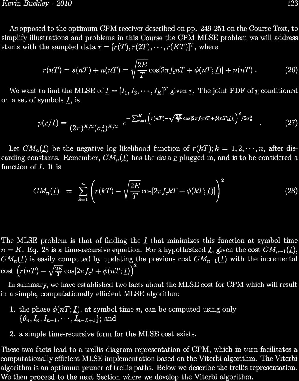
170

171

172

173

174

175

176

177

178

179

180

181

182

183

184

185

186

187

188
189

190

191
192 Kevin Buckley ECE8700 Communication Systems Engineering Villanova University ECE Department Prof. Kevin M. Buckley Lecture 9 cos (2 π f c t) ( ) dt ( ) dt. 2 r(t) π sin (2 f ct) cos (2 π (f c + f) t) max m ( ) dt ( ) dt. 2 sin (2 π(f c + f) t) nt
193 Kevin Buckley Contents 5 Noncoherent Detection & Synchronization Reception with Carrier Phase and Symbol Timing Uncertainty Noncoherent Detection From ML/MAP Detection to ML/MAP Parameter Estimation Carrier Phase Estimation Symbol Timing Estimation Joint Carrier Phase and Symbol Timing Estimation List of Figures 58 Digital communication receiver receiver filter/demodulator and detector Bandpass and equivalent lowpass implementations of a correlator receiver Envelope detector for optimum noncoherent reception Square-law detector for optimum noncoherent reception Square-law detector for optimum noncoherent reception of M = 2 FSK A nonsynchronous binary DPSK receiver A Phase-Locked Loop (PLL) for recovery of an unmodulated carrier A Timing-Locked Loop (TLL) for recovery of symbol timing
194 Kevin Buckley Noncoherent Detection & Synchronization In this Section of the Course we address two common types of digital receiver uncertainty: carrier phase uncertainty, and symbol timing uncertainty. These result due to propagation delay through the channel. One basic approach to dealing with the uncertainty of the carrier phase and symbol timing parameters is to transmit additional signal components, in addition to the communication signal, which facilitates the derivation of these parameters at the receiver. This approach, while important, requires additional resources (e.g. transmit power, bandwidth). The other basic approach is to deal with these uncertainties at the receiver using the received communication signal itself. In this Section we discuss this latter apporach. We detail the problem in Section 5.. We discuss the noncoherent receiver approach to the carrier phase uncertainty problem in Section 5.2. In Section 5.3 through 5.5 we consider estimation of the carrier phase and symbol timing parameters. 5. Reception with Carrier Phase and Symbol Timing Uncertainty Consider a set of symbols s m (t); m =, 2,, M; 0 < t T, with s m(n) (t) received at symbol time n in AWGN. Recall that given the received signal r(t) = s m (t) + n(t) ; 0 < t T () the symbol detection objective is to decide which of the M symbols was transmitted. Figure 58 depicts the problem. The receiver front-end (i.e. the modulation scheme correlator or matched filter) demodulates the received signal and filters it prior to detection or sequence estimation. s m(n) (t) r(t) receiver front end r decision device (e.g. threshold detector) I ^n n(t) T Figure 58: Digital communication receiver receiver filter/demodulator and detector. In Section 3. of this Course, we described the correlator receiver, provided some justification for it, established its sampled output characteristics, and showed its equivalence to the matched filter receiver. This receiver structure correlates the received signal r(t); 0 < t T with each of the modulation scheme basis functions, φ k (t); k =, 2,, N, of the given modulation scheme. This correlation is the inner product, so the correlation receiver forms where N is the modulation scheme dimension and r k = < r(t), φ k (t) > = r = [r, r 2,, r N ] T (2) T = 2 Re{< r l(t), φ kl (t) >} = 0 r(t) φ k (t) dt k =, 2,, N (3) T 0 r l (t) φ kl (t) dt (4)
195 Kevin Buckley where r l (t) is the lowpass equivalent (e.g. quadrature receiver output) of r(t) and the φ kl (t) are the lowpass equivalent basis functions. Figures 59(a,b) show, respectively, the bandpass and equivalent lowpass implementations. In the bandpass implementation illustration, note that the multiplication of r(t) by the φ k (t) represents the demodulation process, since the φ k (t) are bandpass functions (typically cosines with an envelope shaped by a pulse shape g(t)). The integrator is effectively a lowpass filter. The integrator output is sampled when the symbol fills the integrator. For the lowpass equivalent implementation illustration, note the demodulation has already taken place. φ (t) φ* (t),l T r (. ) dt 0 2 T (. ) dt 0 Re r r(t) φ N (t) r r (t) l φ* (t) N,l r (a) T (. ) dt 0 r N (b) 2 T (. ) dt 0 Re r N Figure 59: Bandpass and equivalent lowpass implementations of a correlator receiver. There are two implied assumptions in this receiver that often are not met in application:. It is assumed that the basis functions, the φ k (t) are exactly known to the receiver. Given that we know what the modulation scheme is, this does not on the surface seem like an unreasonable assumption. For the bandpass transmission, these basis functions are similar in form to 2 φ(t) = g(t) cos(2πf c t). (5) E g The sinusoid cos(2πf c t) is called the carrier. The pulse shape g(t) and carrier frequency f c are system specifications. So they can be assumed to be known The received pulse energy, E g, may be a problem, for example when carrier is amplitude modulated, but Automatic Gain Control (AGC) can be employed to effectively deal with this. However, note that the carrier phase is implied to be zero. Basically, this means that it is assumed that the carrier phase as observed at the receiver is known. Given that there is an unknown channel delay, this will not be the case in practice. There is carrier phase uncertainty at the receiver. Below we present several examples of the undesirable consequence of carrier phase uncertainty. So, in any practical digital communication system, this problem must be addressed. Assuming and employing this knowledge of the carrier phase at the receiver is referred to as coherent reception. For a coherent receiver, then, we must somehow recover the carrier phase. The process for achieving this is termed carrier phase estimation or carrier synchronization. An alternative receiver strategy can be implemented one Although there will inevitably be some slight offset between the transmitter and receiver carrier frequency, we will see that this is accounted for by dealing with carrier phase uncertainty.
196 Kevin Buckley that does not require carrier synchronization. Such a strategy is called noncoherent reception. 2. It is assumed that we know when to sample the correlator output that we know when a symbol starts and stops. The symbol duration T is part of the system specification, so it is reasonable to assume it is known. So the assumption reduces to that of knowing when each symbol starts. Again because in practice there is an unknown delay thought the channel, this assumption is not reasonable. There will be symbol timing uncertainty, and thus there is a need for symbol timing recovery. The process for achieving this is termed symbol time estimation or symbol synchronization. Examples of the carrier phase uncertainty problem: As an obvious example, first consider M-ary PSK. A transmitted symbol is of the form s m (t) = 2 E g g(t) cos(2πf c t + θ m ) 0 < t T, (6) where θ m = 2π m; m = 0,,, M. Assume that the received signal is M r(t) = 2 E g g(t) cos(2πf c t + θ m + φ) + n(t) 0 < t T, (7) where φ is an unknown phase shift due to the channel. Clearly, since the receiver objective is to determine θ m, the unknown receiver carrier phase φ is a problem. For example, if φ is ignored, and it has a value of say 2π, then even with no noise the incorrect phase will be M detected at the receiver. Carrier phase uncertainty can be a problem for any modulation scheme for which information is embedded in the carrier phase (e.g. PSK, QAM). As another example, consider the PAM problem described on p. 295 of the Course Text. Let s(t) = A(t) cos(2πf c t + φ) (8) be the received PAM signal, where φ is an unknown phase shift introduced by the channel. For the correlation receiver, let the PAM basis function be φ(t) = 2 T cos(2πf ct + ˆφ) (9) where ˆφ is the assumed carrier phase at the receiver. The correlation receiver multiplier output is s(t) φ(t) = = 2 T A(t) cos(2πf ct + φ) cos(2πf c t + ˆφ) (0) 2T A(t) [ cos(φ ˆφ) + cos(4πf c t + (φ + ˆφ)) ]. ()
197 Kevin Buckley Since the correlator receiver integrator is effectively a lowpass filter, at its output the 4πf c sinusoidal term is attenuated. The remaining term is y(t) = 2T A(t) cos(φ ˆφ). (2) The error between the assumed and actual carrier phase is manifested as cos(φ ˆφ). This suggests that at the correlator receiver output the received symbol can be substantially attenuated. For example, if φ ˆφ = π, y(t) = Noncoherent Detection Noncoherent detection is covered in depth in Section 4.5 of the Course Text. Therein, optimum noncoherent detection is formulated in general, a general optimum detector structure is identified, several modulation schemes are considered, and performance is analyzed. Here, we overview selected discussions from that Section. Noncoherent Detection of Carrier Modulated Signals Consider and digital modulation scheme for which the symbols can be represented as s m (t) = Re { s ml (t) e j2πfct } (3) where s ml (t) is the lowpass equivalent. This includes PAM, PSK, QAM and some binary orthogonal schemes such as FSK. Let the received signal due to a transmitted symbol s m (t) be of the form r(t) = s m (t t d ) + n(t), (4) or equivalently r l (t) = Re { s ml (t t d ) e j2πφ e j2πfct } (5) where t d is an unknown channel induced delay 2 and φ = f c t d. Assume that s ml (t t d ) s ml (t). This implies that either t d << T (where T is the symbol duration) or symbol synchronization has been implemented. Then, the lowpass equivalent of the received symbol is r l (t) = e jφ s ml (t) + n l (t), (6) with complex signal space vector representation r l = e jφ s ml + n l (7) (i.e. r l = r rl + jr il is the complex representation of 2-dimensional r l = [r rl, r il ] T ). For the ML or MAP symbol detection problem formulation, we need p rl (r l /s ml ), the PDF of r l conditioned on s ml. For this, we start with the joint PDf of r l and φ, and marginalize over φ. Letting p φ (φ) denote the prior PDF of random φ, p rl (r l /s ml ) = p rl,φ(r l, φ/s ml ) dφ (8) = p nl (r l s ml ) p φ (φ/s ml ) dφ = p nl (r l s ml ) p φ (φ) dφ (9) 2 For this discussion we do not explicitly address channel attenuation, which would be incorporated into the SNR and controlled with AGC. We do not address multipath channels until later in the course.
198 Kevin Buckley where p nl (n l ) is the noise PDF, and we assume that, conditioned on s ml, the noise n l and phase φ are statistically independent, and that φ does not depend on s ml. The MAP symbol detection problem is then max m P m p n (r l s ml ) p(φ) dφ (20) where P m is the probability of the m-th symbol. It is shown in Subsection 4.5- of the Course Text that in terms of the lowpass equivalent received signal, assuming AWGN and the prior distribution on φ is uniform over 2π, this MAP problem reduces to max m ( ) P m e Em/2N rl 0 s ml I 0 2N 0 where N 0 is the noise spectral level, E m is the energy of the m-th symbols, and I 0 (x) is the modified Bessel function of the first kind and order zero. Since I 0 (x) is a monotonically increasing function of x, for equiprobable and equi-energy symbols, this reduces to the more intuitive problem: max r l s ml. (22) m Eq (22) suggests the optimum noncoherent detector illustrated below in Figure 60. The demodulator is a quadrature receiver. (This figure shows the receiver front end in terms of filters matched to the symbols as opposed to the equivalent structure based on correlation with the modulation scheme basis functions.) This is referred to as an envelope detector since it selects the symbol corresponding to the maximum envelope r l s ml. An equivalent detector, referred to as a square-law detector, is illustrated in Figure 6. s * l(t t) l. r s l. (2) r(t) Demodulator r (t) l s * 2l(T t) l. r s 2l. max m... s * Ml(T t) nt r s l. Ml.... Figure 60: Envelope detector for optimum noncoherent reception.
199 Kevin Buckley s * l(t t) r s l. l. 2 r(t) Demodulator r (t) l s * 2l(T t) r s l. 2l. 2 max m... s * Ml(T t) nt r s l. Ml Figure 6: Square-law detector for optimum noncoherent reception. Noncoherent Decoding of FSK As a special case of the noncoherent demodulator developed above, consider FSK for which the symbols are s m (t) = g(t) cos(2πf c t + 2π(m ) f t) ; m =, 2,, M. (23) The square-law detector, in terms of the bandpass symbols, is illustrated in Figure 62 for M = 2 symbols. cos (2 π f c t) ( ) dt ( ) dt. 2 r(t) π sin (2 f ct) cos (2 π (f c + f) t) max m ( ) dt ( ) dt sin (2 π(f c + f) t) nt. 2 Figure 62: Square-law detector for optimum noncoherent reception of M = 2 FSK.
200 Kevin Buckley Noncoherent Decoding of DPSK Earlier in the Course we introduced binary DPSK as an example of a modulation scheme with memory and noted that one advantage of it is that it facilitates decoding without knowledge of the carrier phase i.e. noncoherent reception is possible by simply detecting the change in initial phase from symbol to symbol. Here we describe a DPSK receiver that does not require carrier synchronization. As we saw in Section 4 of the Course Notes, since DPSK is a modulation scheme with memory, optimum (ML or MAP) estimation of a symbol sequence requires the joint processing of all the symbols in the sequence and all the observed data over the extent of the sequence. In other words, decoupled symbol-by-symbol detection as described in this Subsection is not optimum. Note that an alternative noncoherent detection scheme for DPSK is described in Subsection of the Course Text. Consider binary DPSK, where the transmitted signal is observed at the receiver with unknown phase φ in AWGN. The received signal over the k th symbol duration is r(t) = g(t) cos(2πf c t + θ k + φ) + n(t) kt < t (k + )T (24) where θ k is 0 or π depending on what the k th symbol is and what all the previous symbols were. Consider DPSK and the demodulator depicted in Figure E g g(t) cos(2 π f ct) (k+)t (. ) dt r k,r kt r(t) 2 E g g(t) sin(2 πf c t) r r k T (k+)t (. ) dt kt r k,i r k (k+)t Figure 63: A nonsynchronous binary DPSK receiver. Two correlators are used instead of the one normally required for binary PSK because, with unknown phase φ at the receiver, g(t) cos(2πf c t + θ k + φ) is two dimensional over 0 < φ 2π (i.e. two basis functions are required to represent it over the range of unknown φ). The 2-dimensional observation vector for symbol k is r k = [r k,r, r k,i ] = [ E s cos(θ k φ) + n k,r, E s sin(θ k φ) + n k,i ] (25)
201 Kevin Buckley where E s is the symbol energy (i.e. for binary modulation schemes E s is the same as the bit energy E b ). Eq. (25) can also be conveniently thought of as the complex-valued observation r k = r k,r + jr k,i = E s e j cos(θ k φ) + n k, (26) where n k = n k,r + jn k,i. If, as shown in Figure 63, we form the produce r k r k, then as explained in Subsection of the Course Text, for binary DPSK r k r k Es x k + jy k (27) where x k and y k are real-valued (i.e. x k is the real part of r k r k ) and x k = ± E s + Re{n k + n k } (28) y k = Im{n k + n k }. (29) The noise in y k is statistically independent of that in x k, so that only x k need be processed. In x k, a E s indicates a 0 bit while a E s indicates a. x k has the same form as regular (coherent) PSK, except the noise has twice the power. Thus, compared to binary PSK, performance of binary DPSK using this decoding approach will by (approximately) 3dB worse.
202 Kevin Buckley From ML/MAP Detection to ML/MAP Parameter Estimation Recall the maximum likelihood symbol detection problem addressed in Section 3.2 of this Course. Starting with the signal space representation of the received data for an N-dimensional modulation scheme, the N-dimensional vector r, and the M symbol signal space representation vectors, the s m ; m =, 2,, M, the ML problem is: max s m p(r/s m ) (30) where p(r/s m ) is the likelihood function (i.e. the data vector joint PDF, conditioned of symbol s m having been transmitted, with the received data vector r plugged in). Under the AWGN assumption, this becomes or equivalently, max s m p(r/s m ) = min s m N (2π) N/2 (σn 2 e k= (r k s mk ) 2 /2σn 2, (3) )N/2 N (r k s mk ) 2 = r s m 2. (32) k= This is just the minimum distance decision rule, which suggests a particularly simple ML symbol detection algorithm. The MAP detector is based on the posterior PDF P(s m /r) of s m given r. Using Bayes rule, we have P(s m /r) = p(r/s m)p(s m ) (33) p(r) where P(s m ) is the probability of s m, and p(r) is the joint PDF of r. The MAP detector consists of the following two steps:. Plug the available data r into p(s m /r). Consider the result to be a function of s m, the symbol parameters to be detected. 2. Determine the symbol s m that maximizes this function. This symbol is the MAP detection. Since the denominator term in Eq. 33 is independent of s m, the MAP detector can be stated as: max p(r/s s m ) P(s m ). (34) m Comparing Eqs. 30 and 34, we see that the difference lies in the MAP detector s weighting of the likelihood function by the symbol probabilities P(s m ). If the symbols are equally likely, then the ML and MAP detectors are equal. However, in general they are different. In terms of the primary objective of symbol detection, the MAP estimator is optimum in that it minimizes symbol error rate. The MAP detector is a little harder to design, but just as easily implemented.
203 Kevin Buckley In Section 4 of the Course we saw that the Maximum Likelihood Sequence Estimation (MLSE) formulation is a straightforward extension of ML detection, though algorithmically it is more challenging. MAP sequence estimation is a similar generalization of MAP detection. We can consider these ML and MAP symbol detection and sequenceestimation problems to be discrete-valued parameter estimation problems. The resulting algorithms all involve searching for the lowest cost from a countably finite number of possible solutions. We now turn our attention to ML and MAP estimation of the carrier phase φ and symbol delay τ. The objective is to identify good estimates of these two parameters and to then use them to do coherent detection so as to realize the performance advantage of coherent detection compared to noncoherent detection. φ and τ are continuous-valued parameters. We will see that the ML and MAP estimator problem formulations for these parameters are identical to those for a discrete-valued parameter (e.g. symbol detection) problem. However, the resulting algorithms will be substantially different, due to the need to select the lowest cost over a continuum of possible solutions. Let θ denote the continuous-valued parameter or parameter vector of interest, i.e. θ is φ or τ or {φ, τ}. Let r generally denote the data. Given data r, with joint PDF p(r/θ) conditioned on a value of θ, the ML parameter estimation problem is: max θ L(θ) = p(r/θ) (35) where L(θ) is the likelihood function (the data conditional PDF with the data plugged in). The MAP parameter estimation problem is: max θ p(θ/r) = p(r/θ) p(θ) p(r). = p(r/θ) p(θ), (36) where p(θ) is the known prior PDF of θ. Note that if p(θ) is constant over the range of θ of interest, the ML an MAP estimates are the same. The exact form of the MAP (or ML) problem formulation and resulting processing algorithm will depend of what form the data takes on. In Subsection 5.- of the Course Text, the authors start with the received data waveform r(t) over a symbol period T. For this data, they show that the likelihood function is equivalent to Λ(θ) = exp { N0 T } r(t) s(t; θ) 2 dt, (37) where s(t; θ) would be the received symbol, given θ, if there were no noise. In Subsection 5.-2 of the Course Text, the authors illustrate receiver block diagrams which account for carrier phase and symbol timing uncertainty for several modulation schemes (i.e. binary PSK, M-ary PSK, M-ary PAM and general QAM). These diagrams each includes a carrier recovery block and a symbol synchronization block. These blocks implement, respectively, the φ and τ parameter estimators. We now use ML/MAP formulations to design these blocks. The PAM and QAM diagrams incorporate Automatic Gain Control (AGC). AGC compensates to unknown channel attenuation. This issue is not addressed in the Course Text, so we will not address it here. Note, however, that the AGC block can also be designed using a ML or MAP formulation (for the estimation of a channel attenuation factor).
204 Kevin Buckley Carrier Phase Estimation First assume that the symbol timing parameter τ is known (or that its estimator, the symbol synchronizer block, is to be designed independently). For estimation of the unknown carrier phase φ, assuming AWGN, consider the equivalent likelihood function Λ(φ) = exp { } r(t) s(t; φ) 2 dt. (38) N0 T Expanding the squared term in the integral, and discarding terms that don t effect the maximization, (as shown in the text) we have that { }. Λ(φ) = exp r(t) s(t; φ) dt, (39) which has natural log Λ L (φ) = T T r(t) s(t; φ) dt. (40) In Example 5.2-, p. 297 of the Course Text, the authors discuss the unmodulated carrier case, i.e. where s(t; φ) = A cos(2πf c t + φ). (4) The optimum carrier phase estimate can be found directly by setting d dφ Λ L(φ) = T r(t) sin(2πf c t + φ) dt = 0. (42) This results in { φ ML = tan T r(t) sin(2πf } ct) dt T r(t) cos(2πf. (43) ct) dt Alternatively, as shown in Figure 64, a Phase-Locked Loop (PLL) can be used to generate sin(2πf c t + φ ML ), which after a 90 0 phase shift can be used as the carrier recovery block output required for the coherent receiver structures described in Subsection 5.-2 of the Course Text. r(t) loop filter v(t) sin (2 π f t + φ ^ ) c ML VCO Figure 64: A Phase-Locked Loop (PLL) for recovery of an unmodulated carrier. This PLL consists of a signal multiplier, a loop filter and a Voltage Controlled Oscillator (VCO). The VCO operates to generate a sinusoid of frequency f c with a phase that is
205 Kevin Buckley proportional to the integral of the VCO input v(t). The PLL operates to provide a VCO output that results in the VCO input v(t) = 0. This is, it drives the VCO input to zero. A detailed analysis of this PLL, which can be found in Subsections and of the Text, is beyond the scope of this Course. Concerning unknown carrier phase φ, the real coherent receiver objective is carrier recovery from the received modulated, noisy signal. Subsection of the Course Text describes decision-directed modification of the PLL to achieve this. This too is beyond the scope of this Course. 5.5 Symbol Timing Estimation Now assume that the carrier phase φ is known (or that its estimator, the carrier recovery block, is to be designed independently). For estimation of the symbol timing parameter τ, assuming AWGN, consider the equivalent likelihood function in terms of lowpass signal representation: Λ(τ) = exp { } r l (t) s l (t; τ) 2 dt, (44) N0 where s l (t; τ) = n T I n g(t nt τ). (45) Expanding the squared term in the integral, and discarding terms that don t effect the maximization, (as shown in the text) we have that Λ(τ). = exp { T } r(t) s(t; τ) dt, (46) which has natural log Λ L (τ) = T r(t) s(t; τ) dt = n I n y n (t) (47) where y n (t) = T r l(t) g(t nt τ) dt is the output of the receiver matched filter. For the ML estimate, set d dτ Λ L(τ) = d I n n dτ y n(t) = 0. (48) As shown in Figure 65, a Timing-Locked Loop (TLL) can be used to generate the ML matched filter output sampling times. I n r (t) l Matched Filter g( t) differentiator sampler nt + τ ML VCC adder Figure 65: A Timing-Locked Loop (TLL) for recovery of symbol timing.
206 Kevin Buckley This TLL consists of a matched filter, a sampler, a digital multiplier/summer, and a Voltage Controlled Clock (VCC). The TLL operates to provide a VCC output that drives the VCC input to zero. This TLL is called decision-directed because it employs known symbols at the receiver. These known signals are typically generated as the symbol detector outputs (i.e. the receiver outputs). Thus the term decision-directed.
207 Kevin Buckley Joint Carrier Phase and Symbol Timing Estimation A brief description of a coherent receiver approach based on ML estimation of both carrier phase φ and symbol timing parameter τ is presented in Section 5.4 of the Course Text. This topic is beyond the scope of this Course.
208 Kevin Buckley ECE8700 Communication Systems Engineering Villanova University ECE Department Prof. Kevin M. Buckley Lecture 0 I n * X(z) = F(z) F (z ) y n A(z) = * F (z ) v n (a) v n I n F(z) v n (b) η n I n z z z... f 0 f f L v n (c) η n
209 Kevin Buckley Contents 6 Bandlimited Channels and Intersymbol Interference The Digital Communication Channel and InterSymbol Interference (ISI) Signal Design and Partial Response Signaling (PRS) for Bandlimited Channels A Discrete-Time ISI Channel Model MLSE and the Viterbi Algorithm for ISI Channels List of Figures 66 Representations of a digital communication LTI ISI channel The lowpass equivalent channel output is the superposition of the individual symbol outputs i.e. the I n h(t nt) (a) An ISI digital communication channel (lowpass equivalent shown); (b) an equivalent discrete-time model Illustrations of the Nyquist Criterion of transmission of symbols without ISI across a bandlimited channel Orthogonal expansion of the lowpass equivalent received signal r l (t) Equivalent discrete-time model of an ISI channel Equivalent discrete-time model of an ISI channel Whitening of the sampled matched filter output noise v n Zero configuration for the symmetric noncausal DT channel model DT ISI channel model including noise whitening DT ISI channel model including noise whitening ISI channel model, trellis diagram and Viterbi algorithm pruning for Example ISI channel model, trellis diagram & Viterbi algorithm pruning for Example
210 Kevin Buckley Bandlimited Channels and Intersymbol Interference In this Chapter of the Course we consider the effects of the digital communications channel and its mitigation. This corresponds to Chapter 9 of the Course Text. We assume that the channel is linear and time invariant, and that the noise is AWGN. See Section 9., pp of the Course Text for brief discussions on non-linear channels, time-varying channels, frequency offset, phase jitter and impulses noise. Basically, carrier phase recovery techniques can be used to combat frequency offset and phase jitter. Non-linear channels are beyond the scope of this course, as is impulsive noise which can be countered with channel coding. Timevarying channels are dealt with using adaptive techniques, which will be briefly discussed in a late Section of this Course. The most important characteristic of any realistic communication channel is that it is effectively bandlimited. In Section 6. we first describe a bandlimited, linear, time-invariant channel, and we mathematically model intersymbol Interference (ISI) which is its primary deleterious effect. In Section 6.2 we then introduce signal design methods for eliminating or controlling ISI. In Section 6.3 we then develop a discrete-time ISI model, which will be used in Section 6.4 and in Chapter 7 to develop, respectively, MLSE and channel-equalization techniques for combating ISI at the receiver. 6. The Digital Communication Channel and InterSymbol Interference (ISI) This Section of the Course corresponds to Section 9. and the beginning of Section 9.2 of the Course Text. The goal here is to develop an ISI model of a bandlimited digital communications channel that will allow us to: ) directly apply the MLSE techniques described previously in Chapter 4 of this Course; and 2) develop channel equalization methods in Chapter 7. We will focus on MLSE for N = and N = 2 dimensional linear modulation schemes. The approach easily extends to higher dimensional and nonlinear schemes. Consider QAM, for which PAM and PSK can be consider special cases. The lowpass equivalent symbols are s m (t); m =, 2,, M: s ml (t) = V m e jθm g(t) ; 0 t T m =, 2,, M, () where g(t) is a real-valued pulse shape. For symbol time n and transmitted symbol m = m(n), we can represent the transmitted symbol as s m(n)l (t nt) = V m(n) e jθ m(n) δ(t nt) g(t) (2) where is the symbol rate and δ(t nt) is the impulse function delayed to time nt. T In Section 2.6 of this Course, for a development of spectral characteristics of digitally modulated signals, we established the following equivalent lowpass representation: I n = I n(n) = V m(n) e jθ m(n) = Vm e jθm. PAM, PSK and QAM where, respectively, I n has form: I n = A m (3) I n = e j2π(m )/M I n = V m e jφm.
211 Kevin Buckley With this representation, the real part of I n corresponds to the cosine basis function term on the signal space representation, while the imaginary part corresponds to the sine term. For PAM or 2-PSK, there would be no sine term (i.e. these are N = dimensional modulation schemes). {I n } is the random information sequence, for each symbol time n representing K = log 2 (M) bits. Following the discussion and notation in Section 9. of the Course Text, consider the digital communication channel illustrated as a lowpass equivalent in Figure 66(a). Using the I n representation of symbols, this illustration represents Mathematically, we can think of the lowpass equivalent modulator in this figure as effectively forming I(t) = n I n δ(t nt) (4) and then processing it with an Linear Time-Invariant (LTI) filter with impulse response g(t). The lowpass equivalent of the transmitted signal is v(t) = I(t) g(t) = n I n g(t nt), (5) where actual (real-valued, bandpass) transmitted signal is s(t) = Re {v(t) e j2πfct }. (6) So, here r(t) and z(t) represent, respectively, the lowpass equivalent received signal and lowpass equivalent AWGN. I n v (t) Modulator LTI Channel ( g(t) ) c( t ) r (t) l (a) z (t) I (t) LTI Channel h( t ) r (t) l (b) z (t) Figure 66: Representations of a digital communication LTI ISI channel.
212 Kevin Buckley We assume that the channel is LTI with equivalent lowpass impulse response c(t). In general, c(t) is complex-valued, as is it frequency response C(f) = C(f) e jθ(f) (7) which is the continuous-time Fourier transform (CTFT) of c(t). C(f) and θ(f) are, respectively, the magnitude and phase responses of the lowpass equivalent channel. The envelope delay of this channel (a.k.a. the group delay) is τ(f) = 2π d df θ(f). (8) τ(f) is interpreted as the delay, as a function of frequency, on the lowpass equivalent channel c(t). As with the magnitude and phase responses, and C(f) in general, the envelop delay of the real-valued bandpass channel is given by the lowpass equivalent τ(f) shifted in frequency to f c and folded and shifted to f c. In this Chapter we will assume that c(t) is known (e.g. it has been estimated using training data or a preamble). Example 6.: Consider the lowpass equivalent channel frequency response illustrated below, from which C(f) = ( ) f 2W e j2πτf. C(f) θ (f) W W f W 2π τ W f Using Table of the Course Text (i.e. the CTFT table) and the time-shift and time-scaling properties of the CTFT (from Table 2.0- of the Course Text), we have that c(t) = 2W sinc(2w(t τ)). (9) From Subsection.2.2 of this Course, the corresponding real-valued bandpass LTI channel has impulse response is Re {c(t) e j2πfct } = 2W sinc(2w(t τ)) cos(2πf c t) (0) with frequency response 2 [ ( ) (f fc ) 2W e j2πτ(f fc) + ( ) ( f f c ) 2W e j2πτ(f+fc) ]. ()
213 Kevin Buckley The equivalent lowpass noise, z(t), is AWGN and in general complex-valued (unless v(t) and thus c(t) are real-valued). The lowpass equivalent received signal is r l (t) = v(t) c(t) + z(t) (2) = n I n h(t nt) + z(t) where h(t) = g(t) c(t) (3) is the pulse shape at the channel output. Figure 66(b) shows this compact representation. The lowpass equivalent of the symbol observations at the channel output are of the form I m h(t) = s ml (t) c(t); m =, 2,, M i.e. they are distorted. In processing the received signal, r(t), both noise and channel distortion should be accounted for. For a channel without memory, i.e. for c(t) = δ(t), we are back to the situation considered in Sections 3 & 4 of this Course. That is, r l (t) = n I n g(t nt) + z(t). (4) Then, assuming that there is no memory in the modulation process (e.g. no differential encoding or PRS) and g(t) is restricted to the temporal range 0 t T, we can perform symbol-by-symbol detection on r l (t) as described in Section 3 of the Course. With memory in the modulation process, we can perform MLSE using the Viterbi algorithm as described in Section 4. In general the channel has memory resulting, for example, from multipath propagation. This memory result in an overlap of the individual transmitted symbol waveforms (i.e. the I n g(t nt)) at the receiver. That is, as shown in Figure 67 the pulse shape at the receiver, h(t) = g(t) c(t), will extend in time beyond the channel input symbol width T, creating ISI. This poses two problems: ) the symbols, as observed at the receiver, overlap in time; and 2) unless c(t) is known, h(t) is unknown as are the symbol observations and basis functions for them. The first problem, which we address in this Section, is solved using MLSE (or symbol-by-symbol MAP). We discuss the second problem later on. n I n h(t nt) I h(t) 0 I h(t T) I h(t 3T) 3 T 2T 3T 4T t I h(t 2T) 2 I 4 h(t 4T) Figure 67: The lowpass equivalent channel output is the superposition of the individual symbol outputs i.e. the I n h(t nt).
214 Kevin Buckley In our discussion on symbol detection for an N dimensional modulation scheme, we showed that;. the N matched filters span the symbols; and 2. the noise not represented in r n is statistically independent of the noise in r n. Thus the practice, for the single symbol detection problem, of processing r n instead of r l (t) to detect I n seemed justified. Below, in Subsection 6.3, within the more general context of ISI channels, we show formally that the sequence {r n } is a sufficient statistic for estimating the symbols {I n }.
215 Kevin Buckley Signal Design and Partial Response Signaling (PRS) for Bandlimited Channels This discussion corresponds to Subsections 9.2-, and of the Course Text. ISI at the Receiver Front End Output Consider the transmission of symbols I n ; n = 0,, 2,,. The lowpass equivalent channel output is r l (t) = I n h(t nt) + z(t) (5) where h(t) = n=0 g(τ) c(t τ) dτ (6) is the pulse shape at the channel output (i.e. the convolution of the lowpass equivalent pulse shape into the channel, g(t), and the lowpass equivalent impulse response, c(t), of the LTI channel). Assume that at the receiver a filter matched to the received pulse shape h(t) is applied prior to symbol-rate sampling and subsequent symbol detection or sequence estimation. Assume that the matched filter impulse response is 2 h ( t). The matched filter output is then y(t) = r l (t) h ( t) n=0 I n x(t nt) + v(t), (7) where x(t) = h(t) h ( t) (8) is the pulse shape at the matched filter output, and v(t) = z(t) h ( t) is the noise. Consider sampling this matched filter output at the symbol rate to form T y k = y(kt + τ 0 ) = = n=0 n=0 I n x(kt nt + τ 0 ) + v(kt + τ 0 ) (9) I n x k n + v k (20) where τ 0 represent a bulk channel delay 3 not represented by the channel impulse response c(t), x k = x(kt + τ 0 ) and v k = v(kt + τ 0 ). Eq(20) suggest a DT model of an ISI channel. This model is illustrated in Figure 68. If we assume 4 that x 0 =, then we have that y k = I k + n=0; n k I n x k n + v k, (2) The justification for using a matched filter, or equivalently a correlator, at the receiver front end was presented earlier in Section 3. of this Course. 2 In practice, the matched filter impulse response would be delayed so as to be causal. 3 With symbol timing recovery, we can assume that this bulk delay is τ o = 0. 4 This implies, for example, that AGC is implemented at the receiver.
216 Kevin Buckley I k modulator v(t) c(t) r (t) l * h ( t) y(t) y k (a) z(t) kt h(t)=g(t)*c(t) I n+2 z I I I I k+ z k z k z 0... x 2 x x 0... x k B k y k (b) v k Figure 68: (a) An ISI digital communication channel (lowpass equivalent shown); (b) an equivalent discrete-time model. where the second term on the right side of Eq(2) (i.e. the summation) is the ISI term. So ISI depends on the channel impulse response c(t) through x(t), the pulse shape at the matched filter output. Consider eye patterns which are described and illustrated on pp of the Course Text. Signal Design to Eliminate ISI for a Bandlimited Channel Assume that τ 0 = 0. From Eq(2), to avoid ISI we require that x k = x(kt) = { k = 0 0 k 0. (22) Equivalently, we require that the DTFT of x k be X(e j2πft ) = for all f. From sampling theory, we know that the DTFT of x k is related to the CTFT of x(t) as 5 X(e j2πft ) = T m= X(f + m/t). (23) (In terms of the Course Text notation, B(f) = m= X(f + m/t) = T X(e j2πft ).) In summary, in terms of the frequency characteristics of the pulse at the matched filter output, we have X(e j2πft ) = X(f + m/t) = (24) T m= as our requirement to avoid ISI. 5 Refer to the proof on pp of the Course Text.
217 Kevin Buckley Assume that the channel is bandlimited with two-sided bandwidth 2W, i.e. C(f) = 0 for f > W. Figure 69(a) illustrates X(e j2πft ) for a case where the ISI requirement is not met. The problem is that > W. Equivalently, defining f 2T s = as the symbol rate, the problem T is that f s > 2W the symbol rate is greater than the two-sided channel bandwidth. j2 π f c T X(e ) T X(f) (a) W W 2T T f j2 π f c T X(e ) (b) W W= 2T T f j2 π f c T X(e ) T X(f) (c) W 2T W T f Figure 69: Illustrations of the Nyquist Criterion of transmission of symbols without ISI across a bandlimited channel. From Figure 69(a) and the discussion above, we can make the following three conclusions. # For symbol rate f s > 2W, we can not avoid ISI. # 2 For symbol rate f s = 2W, we can avoid ISI, but only if X(f) = T ( ) f 2W. This is illustrated in Figure 69(b). # 3 For symbol rate f s < 2W, we have some flexibility in the design of X(f). These conclusions reflect the Nyquist Criterion for transmitting symbols across a bandlimited channel that f s 2W is required to avoid ISI.
218 Kevin Buckley As noted above, for f s = = 2W we require X(f) = T ( ) f T 2W, or equivalently, x(t) = 2WT sinc(2wt), (25) where, as defined on p. 7 of the Course Text, sinc(x) = sin(πx). We have no choice in the πx design of x(t), and x k = x(kt) samples x(t) at all the zero-crossings of the sinc function. One problem with this occurs when there is error in the symbol timing recovery. Then x k does not sample the sinc function exactly at its zero-crossings, resulting in ISI. The amount of ISI is dictated by the shape of the sinc functions, which has successive peaks that roll-off as t increases at a rate of. t As noted above, for f s < 2W, we have flexibility in the design of x(t) to meet the requirement that X(f + m/t) = T. (26) m= This flexibility is used to design x(t) such that it has the zero-crossings at t = kt; k = ±, ±2, required to avoid ISI, while having a roll-off that is faster than t so as to be less sensitive to symbol timing recovery error. A popular example of such an X(f) is the raised cosine spectrum described on p. 607 of the Course Text, i.e. X rc (f) = T { [ ( )]} T 2 + cos πt β f β β 2T 2T 0 f +β 2T 0 0 f β f +β 2T 2T, (27) for 0 β. If we assume that the channel has lowpass equivalent frequency response C(f) = ( f ), 2W then x(t) = g(t) g( t) and X(f) = G(f) 2. So we can avoid ISI directly by design of the transmitted pulse shape g(t). For example, to achieve a raised cosine frequency shaping, G(f) = X rc (f) e j2πfto (28) where t 0 controls the position in time of g(t). For a general bandlimited channel, with C(f) = 0; f > W, recall that X(f) = H(f) H (f) = G(f) C(f) C (f)g (f). (29) One way to design X(f), say as X(f) = X rc (f), is to require G(f) = X rc (f) C(f) so that H(f) = X rc (f). Of course, this requires knowledge of C(f) and the design of a pulse shaping filter at the transmitted that depends on the channel frequency response C(f). An alternative design is described in Subsection of the Course Text. (30)
219 Kevin Buckley Partial -Response Signaling (PRS) to Control ISI Consider the ISI model developed above, as described by Eq(20) and illustrated in Figure 68. If we relax the no ISI requirement, Eq(22), in a controlled manner, we can shape the matched filter output pulse and spectrum. For example, we may reduce sensitivity to symbol timing recovery error, or shape the spectrum to match that of the channel (e.g. so we do not transmit power in frequency bands nulled by the channel). In Subsection of the Course Text, several PRS examples are described. A pulse designed such that x k = x(kt) = { k = 0, 0 otherwise (3) is referred to as a duobinary signal pulse. The x k = x(kt) = k = k = 0 otherwise (32) case is called the modified duobinary signal pulse. The modified duobinary signal pulse CTFT is zero at DC, which is advantageous for channels with a DC null. Concerning the ISI model illustrated in Figure 68, assume the model is a causal Finite Impulse Response (FIR) filter on length N, so x k 0 for k = 0,,, N only, i.e. B k = N n=0 x n I k n. (33) Referring back to Subsection 2.5.2, this is the PRS structure introduced as an approach to shaping the spectrum of the transmitted communication signal. In Section 2.6 we observed how PRS can be used to shape this spectrum. In Section 4.3 we showed how to implement MLSE for PRS. So now we see that the PRS structure discussed earlier in the Course is actually a model for signal design and control of ISI for symbol transmission at the Nyquist rate f s = 2W. Alternatively, the PRS structure considered earlier in the course can be used to implement signal design.
220 Kevin Buckley A Discrete-Time ISI Channel Model This corresponds to Section 9.3 of the Course Text. Following the notation in that Section, we will again use r l (t) to denote the lowpass equivalent of the received signal. MLSE Formulation with ISI Let us consider the ML estimation formulation based directly on the lowpass equivalent r l (t). To do this, consider the complete orthonormal expansion of r l (t) in terms of some infinite set of basis functions 6 φ k (t); t ; k =, 2,,. Let r k =< r l (t), φ k (t) > = Then, under reasonable assumptions on r l (t), { } E r(t) r k φ k (t) 2 k= r l (t) φ k(t) dt. (34) = 0. (35) In Figure 70 we illustrate this orthonormal expansion representation of r(t), where the coefficient vector r is infinite dimensional. φ * (t) (. ) dt r r l (t) r φ * (t) 2 (. ) dt r Figure 70: Orthogonal expansion of the lowpass equivalent received signal r l (t). To derive an expression for r in terms of the symbol and noise components, we have that ( ) r k = I n h(t nt) + z(t) φ k(t) dt (36) n = I n n = n I n h kn + z k. h(t nt) φ k (t) dt + z(t) φ k (t) dt (Note that z k = < z(t), φ k (t) > and h kn = < h(t nt), φ k (t) >.) z k is zero-mean complex Gaussian noise with PDF p(z k ) = 2πN 0 e z k 2 /2N 0, (37) 6 Note the these are not the madulation scheme basis fnctions that define the signal space representation.
221 Kevin Buckley where N 0 is the spectral level of passband n(t) so that σ 2 z = 2 N 0. So, r k is complex Gaussian with variance σ 2 z and mean equal to n I n h kn. Note that the z k are mutually uncorrelated and therefore statistically independent. Although r is infinite dimensional, it is comprised on discrete components (the r k s), so we can describe its joint PDF. To do this, let r N = [r, r 2,, r N ] T, and let I be the infinite dimensional vector of symbols I n. The joint PDF of r N is: p(r N /I) = (2πN 0 ) N N e k= r k n Inh kn 2 /2N 0. (38) Let v I (t) = n I n h(t nt) be the noiseless lowpass equivalent received signal conditioned on I. Then, by Parseval s Theorem, the power N k= r k n I n h kn 2 is the power of the representation error r l (t) v I (t). So, ln{p(r/i)} = lim ln{p(r N/I)} =. r l (t) v I (t) 2 dt. (39) N 2N 0 Consider the power metric PM(I) = r l (t) v I (t) 2 dt (40) = r k I n h kn 2. k n Then the equivalent MLSE problem is: max I PM(I). (4) The point here is that we do not need to process, directly, all of r l (t) to compute the ML estimate of the symbol sequence {I n }. This is apparent from Eq. (40). The problem here is that generating and processing the r k is not realistic since producing each r k requires and continuous-time inner product over infinite time and there are an infinite number of r k s. To overcome this problem, consider Eq. (40): PM(I) = r l (t) I n h(t nt) 2 dt (42) n [ ] = r l (t) 2 dt + 2Re In r l (t)h (t nt) dt n InI m h (t nt)h(t mt) dt. n m Let and y n = x n = r l (t) h (t nt) dt (43) h (t) h(t + nt) dt. (44)
222 Kevin Buckley This metric expression is a function of the received data through the y n only, which are sampled outputs of a filter matched to h(t), the pulse shape at the channel output. Given h(t), these y n can be realistically generated. The MLSE problem can now be expressed in terms of the metric CM(I) = 2Re{ n I ny n } n I. ni m x n m = PM(I). (45) m CM(I) is termed the correlation metric. It is the MLSE function to be maximized, and the sequence y n, defined in Eq. (43), is the sufficient statistic of r l (t) for MLSE. Discrete-Time Model for an ISI Channel Starting with Eq. (43) above, for MLSE we need only the sequence where y n = y(t) = = y(nt), r l (t) h (t nt) dt (46) r l (τ) h (τ t) dτ. (47) y n is generated by sampling the output of a filter with impulse response h ( t) with input r l (t), where h(t) = g(t) c(t). This is illustrated in Figure 7(a). We thus have an equivalent discrete-time model, illustrated in Figure 7(b), which has input I n and output y n. I n modulator v(t) c(t) r (t) l * h ( t) y(t) y n (a) z(t) nt h(t)=g(t)*c(t) I n DT LTI system x n y n (b) v n Figure 7: Equivalent discrete-time model of an ISI channel.
223 Kevin Buckley To characterize this equivalent discrete-time channel, note that ( ) y n = I m h(τ mt) + z(τ) h (τ nt) dτ (48) m = I m m h(τ mt)h (τ nt) dτ + z(τ)h (τ nt) dτ = m I m x n m + v n where = I n x n + v n, x n = h (t) h(t + nt) dt = h (t) h( t) t=nt (49) are the coefficients of the equivalent discrete-time channel model. Note that x n = x N, i.e. the equivalent discrete-time channel model has a complex symmetric impulse response. The additive noise, v n = z(τ)h (τ nt) dτ, (50) is Gaussian but not white since it is a sampling of the noise at the output to the receiver filter h ( t). So, y n can be thought of as being generated as the information sequence I n through a DT filter x n superimposed with the Gaussian noise sequence v n. Recall that h(t) = g(t) c(t), where g(t) is the pulse shape into the channel and c(t) is the channel impulse response. h(t) is the pulse shape at the channel output. If g(t) and c(t) are finite duration, which they typically are, then so is h(t) and thus x n will be finite durational. This corresponds to a finite memory (i.e. FIR) ISI channel. the channel impulse response is depicted in Figure 72(a), where for illustration purposes x n is shown as real-valued. Figure 72(b) shows the DT channel model. It is a noncausal model, because of the h ( t) matched filter. In practice, the matched filter would be causal, as would be the DT model. Noise Whitening at the DT Channel Output The problem with the DT model developed to this point is that the noise is not white. To see this, consider y n, which is the sampled output of the receiver filter h ( t) which is matched to the modulation pulse at the channel output. Consider the noise component of it, v n, which is the sampled output of the matched filter h ( t) due to the white noise z(t). The autocorrelation function of v n is R vv [k] = E{v n v n k} (5) = E{ = = = 2 N 0 = 2 N 0 x k. z (τ )h(τ nt)z(τ 2 )h (τ 2 (n + k)t) dτ dτ 2 } E{z (τ )z(τ 2 )}h(τ nt)h (τ 2 (n + k)t) dτ dτ 2 {2N 0 δ(τ τ 2 )}h(τ nt)h (τ 2 (n + k)t) dτ dτ 2 h(t nt)h (t (n + k)t) dt
224 Kevin Buckley * x(t) = h (t) * h( t) x = x(0) 0 x = x(t) x = x( LT) L x = x(lt) L (a) T 0 T 2T LT t I n+l I n+ I n I n I n L z z z z z x L x L+ x0 x L y n (b) v n Figure 72: Equivalent discrete-time model of an ISI channel. Thus, the power spectral density of the noise v n is: S vv (f) = DTFT{R vv [k]} = 2 N 0 X(e j2πft ), (52) where X(e j2πft ), the DTFT of x n, is real-valued since the impulse response x n is complex symmetric. That is, the filter x n is zero-phase. We can see that, in general, v n is not white. To determine the spectral shape of v n, in terms of channel characteristics, again note that the x n are samples of h (t) h( t), i.e. From sampling theory, then x n = x(t) t=nt, x(t) = h (t) h( t). (53) X(e j2πft ) = T l= X(f + l T ), (54) where X(f), the CTFT of x(t), is X(f) = H ( f) H( f) = H( f) 2. (55) Thus, X(e j2πft ) = T l= H( f + l T ) 2. (56)
225 Kevin Buckley Depending on subsequent processing, whitening of v n may or may not be necessary. For example, efficient application of the Viterbi algorithm for MLSE requires that the noise be white, while the white-noise assumption is not critical for channel equalizers. Here we consider whitening v n. Figure 73 shows the processing of y n to whiten its noise component v n. A(z) denotes the whitening filter transfer function, v n the output, and η n the white noise component of the output. A(e j2πft ) = A(z) z=e j2πft is the whitening filter frequency response. y n v n Whitening Filter A(z) v n η n Figure 73: Whitening of the sampled matched filter output noise v n. Since S vv (f) = 2 N 0 X(e j2πft ) and S ηη (f) = S vv (f) A(e j2πft ) 2, to whiten η n we require that X(e j2πft ) A(e j2πft ) 2 = (57) so that S ηη (f) = 2 N 0 = ση. 2 Let X(z) = L n= L x n z n be the transfer function of the DT filter model x n. To realize Eq (57) consider factoring X(z) as X(z) = F(z) F (z ). (58) If such a factorization can be found then, since F (e j2πft ) = F (z ) z=e j2πft, (59) we can write X(e j2πft ) = F(e j2πft ) F (e j2πft ) = F(z) F (z ), (60) z=e j2πft in which case A(z) = will provide the desired whitening, since A(e j2πft ) = F (z ) F (e j2πft ) (6) (62) and thus A(e j2πft ) 2 = F (e j2πft ) F(e j2πft ) = X(e j2πft ) 2. (63)
226 Kevin Buckley To see how X(z) can be factored as in Eq (58), recall that x n is complex symmetric. This means 7 that for every zero z k of the FIR filter transfer function X(z) = L n= L x n z n, there is a zero zk. This zero configuration is illustrated in Figure 74 for a real-valued x n (so that zeros occur in complex conjugate pairs). z plane z k ( z ) * k z k Figure 74: Zero configuration for the symmetric noncausal DT channel model. * z k If we let F(z) = i.e. with zeros at z k ; k =, 2,, L, then F (z ) = L (z z k ), (64) k= L (z z k ) (65) k= will have zeros at z = z k. Thus X(z) can be factored as in Eq (58), where for each pair of X(z) zeros, {z k, z k }, one is assigned to F(z) and the other will be for F (z ). There are 2 L choices for these zero assignments, corresponding to 2 L choices for the whitening filter A(z). For one of these choices, F(z) will be causal. Figure 75(a) illustrates the whitening filter A(z) applied to the DT ISI channel model identified to this point. Figure 75(b,c) show the new DT ISI channel which incorporates the DT whitening filter. The impulse response f n ; n = 0,,, L for this DT ISI channel model is obtained as follows:. Identify h(t) = g(t) c(t). 2. Determine X(e j2πft ) = T l= H( f + l T ) 2, and thus X(z). 3. Factor X(z) as X(z) = F(z) F (z ) (i.e. assign the X(z) zeros to F(z) as indicated above). 4. Derive f n as the inverse z-transform of F(z). 7 See Oppenheim and Schafer, Discrete-Time Signal Processing, Prentice-Hall, 989, p. 265.
227 Kevin Buckley Note that c(t), the channel impulse response, is assumed known. In Section 7 of this Course we address the problem of unknown c(t). The noise at the whitening filter output, η n, is zero-mean AWGN with variance σ 2 η = 2 N 0. I n * X(z) = F(z) F (z ) y n A(z) = * F (z ) v n (a) v n I n F(z) v n (b) η n I n z z z... f 0 f f L v n (c) η n Figure 75: DT ISI channel model including noise whitening.
228 Kevin Buckley MLSE and the Viterbi Algorithm for ISI Channels This Section of the Course corresponds to Subsection of the Course Text. In Section 6.3 of the Course Notes, directly above, we established the equivalent discretetime lowpass channel representation of an ISI communication channel which is applicable for modulation schemes for which the equivalent lowpass transmitted signal is of the form v(t) = n I n g(t nt). (66) This representation is reproduced below in Figure 76. The output is 8 v n = f T I n,l + η n (67) where f = [f 0, f,, f L ] T, I n,l = [I n, I n,, I n L ] T, η n is discrete-time, complex-valued AWGN with variance σ 2 η = 2N 0, and f H f = L k=0 f k 2 =. present input symbol past input symbols I n I z n z z... f 0 f f L I n L v n Figure 76: DT ISI channel model including noise whitening. η n 8 Note that the notation for this whitening filter output, v n, should not be confused with that of the sampled matched filter output noise, v n.
229 Kevin Buckley Since we know that the sequence {v n } forms a sufficient statistic for MLSE of the sequence {I n }, we can formulate this MLSE problem, at time n, in terms of the joint PDF of v n = [v, v 2,, v n ] T conditioned on I n = [I, I 2,, I n ] T : p(v n /I n ) = (πσ 2 η )n n e k= v k f T I k,l 2 /ση 2. (68) Concerning notation, here we represent current time (i.e. the most recent symbol time that we want to optimuze up to) as n, and k represents all symbol time up to n. We then consider incrementing to the next current time n +. The MLSE problem, at symbol time n, is max I n p(v n /I n ). (69) Taking the negative natural log and eliminating constant terms that do not effect the relative costs for different I n s, we have the equivalent problem 9 min I n Λ n (I n ) = PM(I n ) = n v k f T I k,l 2, (70) k= where Λ n (I n ) is the cost of sequence I n. The first n elements of I n are equal to I n, i.e. I n [ : n ] = I n. This suggests that at time n we may be able to time-recursively extend time n results. The Viterbi algorithm efficiently solves this MLSE problem time-recursively (i.e. as n increases). Let Λ n (I n ) = n v k f T I k,l 2 (7) k= = n λ(i k,l ) k= = Λ n (I n ) + λ(i n,l ). The term λ(i k,l ) = v k f T I k,l 2 is the incremental cost of a symbol sequence I n in going from time k to time k. 9 In Chapters 4 & 9 of the Course Text, where MLSE and the Viterbi algorithm are discussed, several notations are used to represent the measure or metric to be optimized. When PM is used, it is maximized, and typically refers to a probability metric. When CM is used, it is minimized, and is sometimes referred to as a correlation of cross-correlation metric. CM is related to but not equal to a Euclidean distance. Here, I start using the notation Λ and refer to it as a cost to be mimimized. As used here, it is close to but not the same as CM of Subsection 9.3- of the Course Text. Here it is a Euclidean distance. I choose Λ so as to get away from the variety of Course Text notations, and because I ve used this notation in other places to represent cost. This is the cost used in subsequent Viterbi algorithm examples, and in the Viterbi algorithm Matlab code provided for Computer Assignment 2.
230 Kevin Buckley At time n there would be M n of these costs, one for each sequence I n. Given these costs at time n, the M n costs at time n (i.e. the cost of the possible sequences I n ) can be easily computed by extending the Λ n (I n ) as in Eq. (7). Thus, each Λ n (I n ) is extended by all λ(i n,l ) consistent with Λ n (I n ). Also note that, although there appears to be M n incremental costs λ(i n,l ) required to extend the costs at time n to those at time n, there are at most only M L+ unique incremental costs, since these costs are determined by I n,l, of which there are M L+ possible values, intead of by the set of M n possible sequences I n from time up to time n. This is what leads to the optimality of the Viterbi algorithm. As with its application to MLSE and MAP sequence estimation for modulation schemes with memory, the idea behind the Viterbi algorithm is to, at time n,. keep only the Λ n (I n ) needed to compute the Λ n (I n ) corresponding to possible optimum I n (i.e. eliminate or prune the I n that can not possibly be optimum); and 2. use the Λ n (I n ) and the λ(i n,l ) to compute the needed Λ n (I n ). Paralleling its development for modulation schemes with memory, we again do this by representing the Λ n (I n ) as paths of a trellis diagram. Since all paths into a trellis state will be extended using the same incremental costs (i.e. incremental costs for time n are computed using only: ) the symbols represented by the previous state and, 2) the new values y n and I n ), only the lowest cost path into each state need be considered). Thus, the Viterbi algorithm to prune the paths. Consider the DT channel model shown in Figure 76. Define the state as the set of outputs of the L delays. For the L elements of the state, and M possible values at each element, there are M L possible states. The trellis maps the M L possible states at any time to the M L possible states at the next time. Associated with this mapping are costs associated with going from one state value to the next. Next we use a couple of examples to illustrate how the trellis represents symbol sequences and their costs, and how the Viterbi algorithm can be used to reduce the computational cost of finding the MLSE solution.
231 Kevin Buckley Example 6.2: Consider symbols that can take on one of M = 2 values, I n = or I n = 0 (e.g. on/off keying - a special case of PAM). Consider an L = delay ISI channel with impulse response vector f = [, 0.5] T as illustrated in Figure 77(a). Assume that the state value at time k = 0 is I 0 = 0. Consider the data points v = 0.2, v 2 = 0.6, v 3 = 0.9 and v 4 = 0.. Use the Viterbi algorithm to determine the MLSE. The incremental cost is: λ k (I k, I k ) = (v k I k 0.5 I k ) 2. So, for example, λ (0, 0) = ( ) 2 =.04 (72) λ 4 (, 0) = (0. 0) 2 =.8 (73) λ 4 (, ) = (0..5) 2 =.96. (74) I n z.5 I n v n (a) η n k=0 k= k=2 k=3 k=4 0 (b) λ (,0)=.64 λ (0,0)=.04 v = λ 2 (0,0)= λ 2 (0,0)=.6 λ 2 (0,0)=.0.64 λ 2 (0,0)=.8 v = 0.6 v = 0.9 v = I 4 =0 I 4 = I 4 =0 I 4 = Figure 77: ISI channel model, trellis diagram and Viterbi algorithm pruning for Example 6.2. The two survivor paths, after stage 4 Viterbi pruning, are highlighted in Figure 77(b). Of these, the best path is represented by a bold solid line, while the other nonpruned path in shown as a bold dashed line. If stage 4 is the last stage, then the MLSE is {I, I 2, I 3, I 4 } = {0,, 0, 0}. (75)
232 Kevin Buckley Example 6.3: Consider symbols that can take on one of M = 2 values, I n = or I n = (e.g. M = 2 PSK). Consider an L = 2 delay ISI channel with impulse response vector f = [.407,.805,.407] T as illustrated in Figure 78(a). Assume that the state value at time k = 0 is {I 0, I } {0, 0}. For M = 2 PSK, this would correspond to no symbols being transmitted prior to symbol time n =. Consider the data points v = 0.407, v 2 =.222, v 3 =.629, v 4 =.629 and v 5 =.85. Use the Viterbi algorithm to determine the MLSE. The incremental cost is: λ k (I k, I k, I k 2 ) = (v k.407i k 0.85I k.407i k 2 ) 2. So, for example, λ (, 0, 0) + λ 2 (,, 0) = 6.64 (76) λ (, 0, 0) + λ 2 (,, 0) =.663 (77) λ (, 0, 0) + λ 2 (,, 0) = 3.32 (78) λ (, 0, 0) + λ 2 (,, 0) = 0. (79) These are the costs of the for paths into stage k = 2 (i.e. the costs for the 4 possible symbol sequences up to state k = 2). I n z I n z I n 2 f 0 f f 2 v = f I + n T n,2 η n (a) η n, k=0, v =0.407 k=2 k=3 k=4 k=5 v = v 3 =.629 v 4 =.629 v 5 = , , , (b) Figure 78: ISI channel model, trellis diagram & Viterbi algorithm pruning for Example 6.3.
233 Kevin Buckley Figure 78(b) shows the trellis diagram and Viterbi pruning through stage 5. After pruning at stage 5, the 4 survivor parts (one into each state) have costs {3.32, 0,.33,.663}. These paths highlighted. The one corresponding to the lowest cost at stage 5 is the one that is completely solid. It corresponds to symbol sequence {I =, I 2 =, I 3 =, I 4 =, I 5 = }. This would be the MLSE if stage 5 was the last. With a path cost of zero, it is tempting to conclude that there is no channel noise, since the received data is exactly the data that would be realized if {I =, I 2 =, I 3 =, I 4 =, I 5 = } were actually transmitted. Finally note that, even if more data is to come, we can say difinitively that the evential MLSE will have {I =, I 2 =, I 3 = }. Practical Issues Trellis Truncation: (See Proakis: p. 246, first paragraph; p. 53, -st paragraph.) In general, given v n ; n =, 2,, K, the MLSE of I K can not be determined for any n until all data up to n = K is processed. For continuous, on-line symbol estimation, i.e. K =, and even for large finite K, this can be impractical. In practice, at any time n the trellis is truncated q samples into the past. That is, at each symbol time n, the best survivor path into stage n is traced back q stage, to stage n q. The value of I n q corresponding to that path is taken as the estimate. Note that this I n q estimate is not guaranteed to be the eventual MLSE. However if all paths at stage n have merged back at stage n q, then I n q will be the MLSE. A useful rule of thumb, which has been shown empirically to result in negligible performance loss, is q 5L where L is the memory depth of the modulation scheme plus channel. A Numerical Issue: For continuous symbol estimation, the numerical value of the minumum cost path to each state grows without bound as time progresses. In practice this probem is resolved by periodically (say at every P th stage) subtracting the smallest path cost from all path costs. Unknown Channel Coefficients: The implementation of MLSE and the Viterbi algorithm for ISI channels, as described above, requires knowledge of the ISI channel coefficients. That is, the coefficient vector f of the equivalent discrete-time model is needed to compute the trellis branch costs. This vector is a function of the actual channel impulse response c(t). In many applications this channel information is not known prior to processing. In these cases the channel coefficients must be either estimated along with the symbols or otherwise dealt with. This issue will be overviewed later, in Section 7.6 of the Course.
234 Kevin Buckley ECE8700 Communication Systems Engineering Villanova University ECE Department Prof. Kevin M. Buckley Lecture Freq. Rsp. (db) Freq. Rsp. (db) Freq. Rsp. (db) 0 (a) channel ω (rad/sample) 20 0 (b) equalizer ω (rad/sample) 0 0 (c) channel/equalizer ω (rad/sample) (d) channel/equalizer f * c opt k Im { I k } 0 Im { v k } 0 Im { Ihat k } Re { I k } Re { v k } Re { Ihat k }
235 Kevin Buckley Contents 7 Channel Equalization Basic Concepts Linear Equalization Channel Inversion Mean Squared Error (MSE) Criterion Additional Linear MMSE Equalizer Issues List of Figures 79 Two DT ISI model and corresponding equalizers The DT ISI channel model after whitening Channel inverse equalizers Noncausal and causal linear time invariance channel equalizers Channel/equalizer characteristics for Example Scatter plots for Example Channel/equalizer characteristics for Example Scatter plots for Example Channel/equalizer characteristics for Example Scatter plots for Example Channel/equalizer characteristics for Example Channel/equalizer characteristics for Example Scatter plots for Example P = 2 cut oversampling and associated DT ISI channel model P = 2 cut fractionally spaced linear equalizer
236 Kevin Buckley Channel Equalization This Chapter of the Course corresponds to Sections 9.4 & 9.5 of the Course Text. As in the last Chapter of these Course Notes, here we address the problem of channel induced ISI. Again, we assume a linear channel, however we now take a very different approach. Instead of sequence estimation, we will first try to compensate for (or equalize) the effect of the channel using a receiver filtr (called an equalizer), and we will then perform detection of individual symbols. 7. Basic Concepts Following are several important points concerning the channel equalization approach to mitigating ISI:. the channel equalizer will process a discrete-time receiver signal, i.e. the sampled output of a matched filter. 2. Some channel equalization algorithms are developed ignoring additive noise. Such algorithm tend to perform worse than algorithms which account for noise, especially when the channel has nulls in its frequency response. 3. The two basic equalizer structures considered here are: ) the linear equalizer structure; and 2) the Decision Feedback Equalizer (DFE) structure. 4. There are two basic modes for the design and implementation of either linear equalizers or DFEs: ) the training mode (based on transmitted training symbols that are known at the receiver); and 2) the decision directed mode (for previous detected symbols replace training symbols at the receiver). 5. The processing will not be optimal with respect to the symbol detection or sequence estimation criteria that we have considered previously (e.g. ML or MAP). Equalizers will be designed using optimum filtering formulations (e.g. channel inversion or minimum mean squared error (MMSE) filter design). 6. Optimum equalizer filter design algorithms require knowledge of the channel impulse response. This shortcoming can be effectively elleviated using and adaptive filtering algorithm which will self-design the equalizer so as to approximate the optimum equalizer. These issues will be addressed in this Chapter of the Course.
237 Kevin Buckley Figure 79 is an illustration of the discrete-time channel model developed previously. An equalizer, with transfer function C(z), is applied to the channel output of the whitening filter F (z ). Alternatively, the whitening filter can be eliminated and the equalizer C (z) can be applied directly to the sampler output y k. Recall that we represent the equivalent discretetime ISI channel model, before whitening, with impulse response x k or equivalently transfer function X(z). We also represent the discrete-time ISI channel model, after whitening, with impulse response f k or transfer function F(z). In both cases the output of the equalizer is denoted Îk since it is an estimate of the symbol sequence I k. There are two fundamentally different approaches to ISI channel equalization:. Channel Inversion, where C(z) = or C (z) = is the ideal objective, and the F(z) X(z) ideal output is Î k = I k + n k () where n k is additive noise; and 2. Minimization of mean squared error (MSE), where min C(z) E{ I k Îk 2 }, (2) or some similar optimization problem is solved. The channel inversion approach will assure the elimination of ISI. However, for a channel with spectral nulls over some frequency band, an equalizer designed based on channel inversion will have large gain over that frequency band, and thus will have the disadvantage of significant amplification of any noise in that frequency band. With the MMSE design approach, there is no guarantee that the signal at the equalizer output will not be distorted (i.e. there may be some residual ISI), but there will be an optimum tradeoff (in the MSE sense) between signal distortion and additive noise suppression. The transfer function notation C(z) and C (z) implies that the equalizer is linear and time invariant. However, we will additionally consider nonlinear decision feedback equalizers and time-varying data adaptive equalizers. F(z) I k X(z) * F (z ) v k C(z) ^ I k v k C (z) or ^ I k Figure 79: Two DT ISI model and corresponding equalizers.
238 Kevin Buckley For MMSE equalizer design purposes, we will need the correlation function of the received discrete-time signal we will be equalizing. Consider, for example, equalizing the whitening filter output v k. Figure 80 illustrates the FIR channel to be equalized. The disctere-time (DT) whitened channel output is v k = b k + η k (3) where η k is discrete-time AWGN with variance ση 2 = 2N 0 (in general complex-valued), and b k = L n=0 f n I k n is the signal component of the channel output. The correlation function of v k is R v,v (k) = E{v n vn k} = ση 2 δ k + R bb (k) (4) where R bb (k) = R II (k) f k f k. If we assume that R II(k) = E{I n I n k } = δ k (i.e. I k is an uncorrelated symbol sequence), then where x k = L k n=0 f n f n+k. Then, x k k = 0,,, L R bb (k) = x k k =, 2,, L 0 otherwise (5) R vv (k) = σ 2 η δ k + R bb (k) = σ 2 η δ k + L k n=0 f n f n+k. (6) I k z z z... f 0 f f L b k v k Figure 80: The DT ISI channel model after whitening. η k
239 Kevin Buckley Linear Equalization In this Section we will consider channel inversion based design of a linear time-invariant (LTI) equalizer C(z). The design of C (z) would proceed in a similar manner. We consider both an FIR filter structure and an unrestricted LTI structure Channel Inversion Channel inversion equalization is also referred to a zero-crossing equalization and peak distortion criterion based equalization. Figure 8(a) shows the general equalizer problem. Let q k = c k f k = j= c j f k j. (7) Then Î k = I k q k = The zero-crossing design objective is j= I j q k j = q 0 I k + (8) or Taking the z-transform, we have q k = δ k ; all k, (9) c k f k = δ k. (0) C(z)F(z) = or C(z) = F(z). () This is the channel inverse equalizer. Figure 8(b) illustrates this equalizer. (The channel inverse equalizer for the DT channel model without whitening C (z) is shown in Figure 8(c)). Previously we have shown that the noise before the whitening filter, i.e. v k, has power spectral density S vv (f) = 2N 0 X(e j2πft ) f 2T, (2) the noise power spectral density of the equalizer output noise is then S nn (f) = C (e j2πft ) 2 S vv (f) (3) = X(e j2πft ) X (e j2πft ) 2N 0 X(e j2πft ) 2N 0 = X(e j2πft ) since X(e j2πft ) is real-valued (i.e. x k is complex symmetric). Recall that X(e j2πft ) = T l= H(f + l T ) 2. (4)
240 Kevin Buckley Q(z) I k v k ^I k F(z) C(z) (a) η k I k F(z) v k F (z) ^ I k (b) η k I k X(z) y k X (z) ^I k (c) v k Figure 8: Channel inverse equalizers. X(e j2πft ) can have spectral nulls if H(f) has. If this is the case, then S nn (f) will have large gains at some frequencies, and the noise power, σ 2 n = /2T /2T S nn (f) df (5) can be very large. Noise amplification is the major limitation of channel inversion equalization. The above discussion assumes no restriction on C(z). Often, the equalizer will be restricted to be FIR, i.e. C(z) = c K z K + c K+ z K + + c 0 + c z + + c K z K, (6) (see p. 649 of the Course Text) with corresponding output, Î k = K j= K c j v k j. (7) In general, a channel F(z) or X(z) can not be prefectly inverted with an FIR equalizer. This is because the channel is FIR, and an FIR system can not be inverted with an FIR system (i.e. only poles can exactly cancel zeros, and FIR transfer function can not invert an FIR transfer function). In practice, this noncausal FIR filter can be realized by designating the current output of the whitening filter as v k+k.
241 Kevin Buckley Mean Squared Error (MSE) Criterion Consider the DT linear time invariant channel models established in Section 3 of the Course. This model has as its input the symbol sequence I k. It output could be, for example: ) the sampled output of the receiver demodulator; or 2) the sampled output, denoted y k, of the receiver filter matched to the pulse shape h(t) at the channel output; or 3) the output, denoted v k, of the DT filter which noise-whitens the sampled matched filter output y k. As an example we will consider processing v k. Here we consider a DT linear time invariant equalizer with input v k, transfer function C(z), impulse response c k, and output sequence Îk which is to be considered an estimate of the symbol sequence I k. Note that Îk is implicitly a function of the equalizer transfer function C(z), or equivalently the equalizer impulse response c k. Consider, as equalizer design objective, the MSE cost function J = E{ I k Îk 2 }. (8) The Minimum MMSE (MMSE) equalizer is the solution to the problem min C(z) J. (9) That is, the design problem is to select C(z) (or equivalently c k ) to minimize the cost J. FIR C(z) First consider an equalizer which has a structure which is constrained to be FIR. The formulation for this in the Course Text, shown here in Figure 82(a), is noncausal. K is the FIR equalizer memory depth design parameter. The MMSE will decrease as K increases. However, increasing K increases computational requirements, and as we will see, for adaptive equalizers increasing K can actually lead to increased MSE. The formulation we will use is shown in Figure 82(b). It is a causal FIR equalizer of length K + and latency (delay). K and are design parameters. In terms of the noncausal equalizer design parameter K, reasonable values for K and are K = 2K and. If the channel has some bulk propagation delay, say of B symbols, then > B is desirable. For example, = B + K is reasonable. 2 The output of the causal FIR equalizer is Î k = c k v k = K c j v k j = c T v k (20) j=0 where v k = [v k, v k,, v k K ] T and c = [c 0, c,, c K ] T is the FIR equalizer coefficient vector. Define the error as e k = I k c T v k, (2) which is a linear function of the coefficient vector c. Consider the cost J = J(c/K, ) = E{ e k 2 }, (22)
242 Kevin Buckley v k+k v k+k z z z... c K c K+ c 0 v k z z v k K... c K I k (a) v k v k v k K z z z c 0 c... c K I k (b) Figure 82: Noncausal and causal linear time invariance channel equalizers. where the notation J(c/K, ) explicitly shows that the cost is a function of c and it depends on given values of K and. We have that J(c/K, ) = E{ I k c T v k 2 } (23) = E{ I k 2 } E{c T v k I k } E{I k v H k c } + E{c T v k v H k c } = σ 2 I c T ζ ζ T c + c T Υ c where ζ = E{I k v k} is the cross correlation vector between I k and v k and Υ = E{v k v T k } is the covariance matrix of v k. Note that since Υ is the correlation matrix of v k, it is symmetric and positive definite. If v k is complex-valued, assumed above, then Υ is complex symmetric.
243 Kevin Buckley The MMSE problem is min c J = σ 2 I c T ζ ζ T c + c T Υ c. (24) The solution can be obtained by solving the K + linear equations c J = 0 K + or by completing the square on J. Below we take the latter approach. Note that, since the covariance matrix is positive definite, Υ exists, and for any w we have that w T Υ w > 0. Also, Υ T = Υ and (Υ ) T = (Υ ) since the covariance matrix is complex symmetric. Therefore J = σ 2 I ζ T (Υ ) ζ + (c Υ ζ) T Υ (c Υ ζ). (25) Since Υ is positive definite, it is clear that J is minimized with and, given c opt, the MMSE is ζ = E{I k v k } = c opt = Υ ζ (26) J min = σ 2 I ζh (Υ ) ζ. (27) We assume throughout that I k is an uncorrelated sequence. Then the (K + ) cross correlation vector is f f E{I k ( Ll=0 f l I k l + η k) } E{I k ( Ll=0 f l I k l + η k) }. E{I k ( Ll=0 f l I k K l + η k ) } =. f (28) We assume throughout that the noise is white. Then the (K + ) (K + ) covariance matrix is R vv (0) R vv ( ) R vv ( K ) Υ = E{v k vt k } = R vv () R vv (0) R vv ( K + )....., (29). R vv (K ) R vv (K ) R vv (0) where R vv (0) = ση 2 + L l=0 f l 2, R vv (m) = L m l=0 f l fl+m ; m =, 2,, L, R vv ( m) = Rvv (m); m =, 2,, L, and R vv(m) = 0; m > L. For real-valued I k, f and c, forget about the conjugates. To design c opt, Υ and ζ are required. For these, you need either:. σ 2 n and the equivalent discrete-time channel model coefficients; or 2. the whitening filter output v k covariance function R vv (k) and the cross correlation function E{I k v k }.
244 Kevin Buckley Example 7.: Consider M = 4 PSK and an ISI channel with equivalent DT channel model impulse response vector f = [.5,.72,.36] T. The received signal is v k = f T I k + η k (30) where I k = [I k, I k, I k 2 ] T, I k = I m(k), and AWGN η k. Assume that the SNR/bit at v k, in db, is γ b (db) = 0 log 0 ( E{I 2 k } f T f 4 σ 2 η ) = 2 db. (3) Consider a FIR MMSE equalizer order K = 6 (i.e. 7 coefficients) and latency = 4. Determine the MMSE equalizer coefficient vector c opt. Using Matlab to compute Eq (26) for this problem, we get c opt = [.92,.2377,.4708,.8740,.3557,.270,.0562] T. (32) Figure 83 shows characteristics of the solution. Figure 83(a) shows the frequency response of the channel. Over the discrete-time frequency range π ω π, the gain does not vary from one by more that 5dB. Figure 83(b) shows the frequency response of optimum equalizer. Note that, in combating the channel effect, the equalizer provides gain where the channel attenuates, and attenuation where the channel has gain. Figure 83(c) shows the combined channel/equalizer frequency response. We see that the equalizer is fairly successful at equalizing the frequency magnitude response. It would be more effective at higher SNR and/or longer equalizer filter length. Figure 83(d) shows the combined channel/equalizer impulse response. To completely eliminate ISI while providing a latency of = 4, this impulse response would have to be δ k 4 an impulse delayed by 4. We see that this MMSE equalizer is very effective. Figure 84 shows the Example 7. scatter plots for 000 samples of I k, v k and Îk. We conclude that this channel is easily equalized with a linear equalizer.
245 Kevin Buckley f * c opt Freq. Rsp. (db) Freq. Rsp. (db) Freq. Rsp. (db) (a) channel ω (rad/sample) 5 0 (b) equalizer ω (rad/sample) 0 0 (c) channel/equalizer ω (rad/sample) (d) channel/equalizer k Figure 83: Channel/equalizer characteristics for Example Im { I k } 0 Im { v k } 0 Im { Ihat k } Re { I } k Re { v } k Re { Ihat } k Figure 84: Scatter plots for Example 7..
246 Kevin Buckley Example 7.2: the same as Example 7., except that f = [.8,.6] T, γ b = 9 db, K = 6 and = 9. Figure 85 shows characteristics of the solution. f * c opt Freq. Rsp. (db) Freq. Rsp. (db) Freq. Rsp. (db) (a) channel ω (rad/sample) 5 0 (b) equalizer ω (rad/sample) 0 0 (c) channel/equalizer ω (rad/sample) (d) channel/equalizer k Figure 85: Channel/equalizer characteristics for Example 7.2. Results are somewhat similar to those in Example 7.. The primary difference is that the channel now has a moderate null at DC, as shown in Figure 85(a). Figures 85(b,c) show that the equalizer is not very successful at equalizing the channel attenuation at low frequencies, even though, compared to Example 7., a longer equalizer filter was used. Figure 85(d) shows that there will be some residual ISI after equalization. Figure 86 shows the Example 7.2 scatter plots for 000 samples of I k, v k and Îk. We conclude that a linear equalizer can be somewhat effective with this channel, but that the moderate null does limit performance Im { I k } 0 Im { v k } 0 Im { Ihat k } Re { I k } Re { v k } Re { Ihat k } Figure 86: Scatter plots for Example 7.2.
247 Kevin Buckley Example 7.3: Again consider M = 4 PSK and an ISI channel, this time with equivalent DT channel model impulse response vector f = [.407,.85,.407] T. Again let γ b = 2 db. Consider a FIR MMSE equalizer order K = 6 and latency = 4. Using Matlab to compute Eq (26) for this problem, we get c opt = [.0083,.86,.6766,.6342,.6766,.86,.0083] T. (33) Figure 87 shows characteristics of the solution. Figure 87(a) shows the frequency response of the channel. Notice the high frequency null, which makes this channel difficult to equalize with a linear filter. Figure 87(b) shows the frequency response of optimum equalizer. Note that, in combating the channel effect, the equalizer tries to provide gain at higher frequencies. The filter is successful in the mid frequency range. However, at the highest frequencies, inverting the channel frequency response would require substantial gain. Since, at 2dB, the noise level is not insignificant, the equalizer can not provide this gain without significant amplification of the noise. Thus, the optimum equalizer shuts off at high frequency. Figure 87(c) shows the combined channel/equalizer frequency response. Note that, with gain close to 0dB, equalization is effective at lower frequencies where the channel attenuation is not too significant. However, the MMSE linear equalizer can not provide the gain around ω = ±π required to invert the channel. Figure 87(d) shows the combined channel/equalizer impulse response. To completely eliminate ISI while providing a latency of = 4, this impulse response would have to be δ k 4 an impulse delayed by 4. Instead, we see significant ISI. Combining the frequency response and impulse response results, we can see the ISI/noise-gain tradeoff characteristic of the linear MMSE equalizer. Figure 88 shows the Example 7.3 scatter plots for 000 samples of I k, v k and Îk. We conclude that, because of the deep spectral null, the MMSE linear equalizer fails to equalize this channel.
248 Kevin Buckley f * c opt Freq. Rsp. (db) Freq. Rsp. (db) Freq. Rsp. (db) (a) channel ω (rad/sample) 5 0 (b) equalizer ω (rad/sample) 0 0 (c) channel/equalizer ω (rad/sample) (d) channel/equalizer k Figure 87: Channel/equalizer characteristics for Example Im { I k } 0 Im { v k } 0 Im { Ihat k } Re { I k } Re { v k } Re { Ihat k } Figure 88: Scatter plots for Example 7.3.
249 Kevin Buckley Example 7.4: Same as Example 7.3, except with γ b = 25 db. Again using Matlab to compute Eq (26) for this problem, we get c opt = [.2452,.7522,.5374, 2.654,.5374,.7522,.2452] T. (34) Figure 89 shows characteristics of the solution. Results are somewhat similar to those in Example 7.3. The primary difference is that, with the significantly lower noise level, the optimum filter does provide some gain at high frequencies to combat the high frequency channel null. This is shown in Figure 89(b). However, as indicated in Figures 89(c,d), the channel is still not effectively equalized, and significant ISI remains. f * c opt Freq. Rsp. (db) Freq. Rsp. (db) Freq. Rsp. (db) (a) channel ω (rad/sample) (b) equalizer ω (rad/sample) 0 (c) channel/equalizer ω (rad/sample) (d) channel/equalizer k Figure 89: Channel/equalizer characteristics for Example 7.4.
250 Kevin Buckley Example 7.5: Same as Example 7.4, except with K = 38. Figure 90 shows characteristics of the solution. Results are somewhat somewhat better those in Examples 7.3 and 7.4. This time, with the longer FIR equalizer, the equalizer does a very good job of inverting the channel frequency response except at the higher frequencies very near the channel spectral null. We can see this by comparing Figures 87(a,b), and by inspection of Figure 89(c). However, Figure 89(d) shows that the channel is partially equalized, and some ISI remains. Figure?? shows the Example 7.5 scatter plots for I k, v k and Îk. We conclude that this channel is not easily equalized with a linear equalizer. Increasing K beyond that of Example 7.5 will not improve performance significantly. A linear equalizer of any length can not effectively equalize a channel with a deep spectral null, regardless of the SNR. Freq. Rsp. (db) Freq. Rsp. (db) Freq. Rsp. (db) 0 (a) channel ω (rad/sample) 20 0 (b) equalizer ω (rad/sample) 0 0 (c) channel/equalizer ω (rad/sample) (d) channel/equalizer f * c opt k Figure 90: Channel/equalizer characteristics for Example Im { I k } 0 Im { v k } 0 Im { Ihat k } Re { I } k Re { v } k Re { Ihat } k Figure 9: Scatter plots for Example 7.5.
251 Kevin Buckley Additional Linear MMSE Equalizer Issues Unconstrained Linear Equalizer The formulation of the MSE equalizer discussed above in Subsection assumes that the equalizer is FIR. That is, the equalizer is constrained to have an FIR structure. The unconstrained MSE equalizer can also be derived. As with the unconstrained channel inversion equalizer, the formulation is in terms of the equalizer transfer function. It is more enlightening to formulate the unconstrained MSE equalizer problem in terms of the transfer function C (z) which is applied to the output of the sampler, without any whitening filter. The unconstrained MMSE equalizer is derived on pp of the Course Text. Its transfer function is C opt (z) = X(z) + N 0. (35) Compared to the unconstrained channel inversion equalizer, for which C (z) =, we see X(z) that with the MMSE equalizer additive white noise is accounted for by the additional N 0 term in the transfer function denominator. For high SNR (i.e. for low noise level N 0 ), the MMSE transfer function approaches C opt(z) = X(z). (36) In this case, the MMSE equalizer inverts the channel. On the other hand, for low SNR (i.e. for high noise level N 0 ), the MMSE transfer function approaches C opt (z) = N 0. (37) The MMSE equalizer transfer function goes to the constant N0, which indicates that the equalizer provides no frequency selective filtering. Instead it basically shuts down. In between these two limiting cases, the MMSE filter optimally trades-off additive white noise suppression and channel inversion. From a channel inversion equalizer point of view, the additional additive N 0 term in the denominator of equalizer transfer function acts as a regularization term, controlling the noise gain by limiting the gain in the frequency response C opt (ej2πft ). Design of C opt (z) requires: ) knowledge of X(z), which in turn requires knowledge of the channel equivalent lowpass impulse response c(t); 2) the assumption that the lowpass equivalent additive channel/receiver noise z(t) is white; and 3) knowledge of the spectral level N 0 of the additive noise z(t).
252 Kevin Buckley Colored Noise and Interference Cancellation When the additive noise z(t) is not white, for example because the receiver noise is colored or the receiver picks up interference signals, then C (z) = X(z)+N 0 is not the optimum MMSE equalizer. Let S zz (f) be the PSD of the additive channel/receiver noise. It can be shown that the optimum equalizer has a transfer function of the form C opt(e j2πt ) = X(e j2πt ) X(e j2πt ) 2 + S vv (f), (38) where S vv (f), the PSD of the noise v n at the sampler output, is S vv (f) = T l= S zz (f + l T ) H(f + l T ) 2, (39) and as before H(f) is the CTFT of the pulse at the channel output. Comments on MSE Equalizer Performance Figure on p. 654 of the Course Text shows the impulse responses of three equivalent discrete-time channels for which equalizer performance was studied. The 2-nd channel is one that you are considering in computer assignments. Figure shows the corresponding channel frequency responses. Note that two of the channels have spectral nulls in their frequency responses. For M = 2 symbol antipodal PAM, Figure compares the performance of the MMSE equalizer for each channel. Symbol error probabilities are shown for the three MMSE equalized channels along with the ideal performance realized when there is no channel induced ISI. Note that rather long (K + = 3 tap) equalizers were used for all channels, with = 6. Even with the large K, equalizer performance is not good for the two channels that have spectral nulls in their frequency responses. Channel inversion equalizers would perform even worse for the channels with spectral nulls, since channel inversion would result in significant noise gain. These results point to the principal limitation of linear equalizers. Linear equalizers usually do not perform well for channels that have spectral nulls in there frequency response.
253 Kevin Buckley
254 Kevin Buckley Fractionally Spaced Linear Equalizers To this point, in using the discrete-time equivalent model of the communication system and ISI channel, we have been assuming that the receiver sampler operates at the symbol rate. This sampling rate was justified using a sufficient statistic argument for MMSE. Looking back at the argument that established the optimality of sampling at this rate, it required that the channel impulse response (explicitly the channel output pulse shape) is known, so that the receiver output can be matched filtered prior to sampling. When the channel impulse response in unknown, or when the matched filter in not implemented, sampling at the symbol rate may no longer be adequate for generation of sufficient statistics for MMSE. T Sampling at a higher rate can then result in improved performance. When the channel impulse response c(t) is not known, the receiver filter is commonly matched to g(t), and equalizers are sometimes operated at a higher sampling rate to improve performance. The Figure 92(a) depicts this oversampling scheme, where the sample rate is T with T < T. Typically PT = T for positive integer P, and we refer to P as the number of cuts. For example, for P = 2 cuts, Figure 92(a) illustrates the sampling. Figure 92(b) shows the equivalent DT model, where f i = [f i,0, f i,, f i,l ] T ; i =, 2. x o x o x o x o x o x o x o x o 0 T 2T 3T 4T 5T 6T 7T x v,k (a) o v 2,k f v,k I k η,k f v 2 2,k (b) η 2,k Figure 92: P = 2 cut oversampling and associated DT ISI channel model.
255 Kevin Buckley Consider the P = 2 cut MMSE fractionally spaced linear equalizer illustrated in Figure 93. Assume that E{η,k η 2,j} = 0 for all k, j. Let v k = [v T,k, vt 2,k ]T with v i,k = [v i,k, v i,k,, v i,k K ] T, and c = [c T, ct 2 ]T with c i = [c i,0, c i,,, c i,k ] T. Then Î k = c T v k. (40) In Homework #7 you are asked to derive the expression for the MMSE coefficient vector c opt for this equalizer. v,k v,k z z z v,k K... c,0 c, c,k I k v v v z z z 2,k 2,k 2,k K... c c c 2,0 2, 2,K Figure 93: P = 2 cut fractionally spaced linear equalizer. For P > 2 cuts, we simply extend Figure 93, using P FIR filters. Array Linear Equalizers Consider receiving a transmitted digital communication signal with P receiver antenna. Assume that the channel from the transmitter to each receiver is an ISI channel. Assume each receiver antenna has front-end electronics and a sampler so as to generate a DT signal v i,k ; i =, 2,, P. Each of these DT signals can be modeled as the output of an equivalent DT model of the channel from the transmitter to its receiver antenna. We can consider each of these signals as a cut, which leads to a linear equalizer structure and design problem analogous to the fractionally spaced linear equalizer. In Homework #8 you are asked to design a P = 2 array linear equalizer.
256 Kevin Buckley ECE8700 Communication Systems Engineering Villanova University ECE Department Prof. Kevin M. Buckley Lecture 2 v k v k v k K z z z c 0 c... c K I k ~ I k z z... bk 2 b 2 b z (a) (b) I k Im { I k } 0 0 Im { Ihat k } Re { I k } Re { v k } Re { Ihat k }
257 Kevin Buckley Contents 7 Channel Equalization Basic Concepts Linear Equalization Decision Feedback Equalization List of Figures 94 The Decision Feedback Equalizer (DFE) An equivalent block diagram of the DFE in training mode Channel/equalizer characteristics for Example Scatter plots for Example Channel/equalizer characteristics for Example Scatter plots for Example P = 2 cut (i.e. fractionally spaced or array) DFE
258 Kevin Buckley Channel Equalization 7. Basic Concepts 7.2 Linear Equalization 7.3 Decision Feedback Equalization Corresponds to Section 9.5 of the Course Text. First consider the linear equalizer described in Section 4.2 above. We can look at the function of this equalizer as one of linearly combining the samples in the equalizer delay line in such a way that all symbols appearing in the delay line, except I k, are canceled out. As illustrated in the last section, this can not always be done successfully. In particular, this linear ISI cancellation can not be accomplished without significant noise amplification when the channel has spectral nulls. The rationale behind using a decision feedback equalizer is that symbols appearing in the linear equalizer delay line can alternatively be canceled using previous estimates generated by the receiver. Specifically, at time k, estimates Îk j; j =, 2, exist that might be used to effectively cancel the symbols I k j ; j =, 2, appearing in the linear equalizer delay line. That is, past symbol decisions can be fed back and used by the equalizer to estimate (i.e. detect) the symbol of present interest. Figure 94 depicts a Decision Feedback Equalizer (DFE), which employs these past symbol estimates. At time k, the estimated symbol Îk is detected to form the symbol estimate Ĩ k which is fed back through another linear filter b of length K 2 to assist the estimation of subsequent symbols. This feedback occurs when the switch at on the right side of Figure 94 is in the (a) position. The DFE is a nonlinear equalizer because of the nonlinearity (the detector of decision device) employed to generate Ĩk from Îk. We refer to c as the feed-forward filter, and b as the feedback filter. v k v k v k K z z z c 0 c... c K I k ~ I k z z... bk 2 b 2 b z (a) (b) I k Figure 94: The Decision Feedback Equalizer (DFE).
259 Kevin Buckley The DFE design problem is to determine c and b, the feed-forward and feedback DFE coefficient vectors. To do this, note that Î k = K K 2 c j v k j + b j Ĩ k j () j=0 j= = c T v k + b T Ĩ k where c = [c 0, c,, c K ] T, (2) b = [b, b 2,, b K2 ] T, (3) v k = [v k, v k,, v k K ] T, (4) and Ĩ k = [Ĩk, Ĩk 2, Ĩk K 2 ] T. (5) To derive a design equation, first consider the error e k = I k Îk. (6) The problem with this error is that it is a highly nonlinear function of c and b, since Îk is a function of Ĩk j; j =, 2,, K 2 which are functions of c and b. Thus, minimizing the mean squared value of (6) would be very difficult. General closed form expressions of optimum c and b do not exist. Consider the alternative error e 2 k = I k I k, (7) where I k is obtained from () by replacing the Ĩk j with I k j. That is, I k = K K 2 c j v k j + b j I k j (8) j=0 j= = c T v k + b T I k = w T x k, where w = [c T, b T ] T and x k = [v T k, I T k ] T. Since I k is not a function of c and b, e 2 k is a linear function of c and b, and an optimum expression for the DFE coefficients can be derived (optimum in the sense of the mean squared value of e 2 k, which is not of direct interest). Let the cost be J = J(w/K, K 2, ) = E{ e 2 k 2 } = E{ I k I k 2 }. (9) The solution to the problem min w J(w/K, K 2, ) (0)
260 Kevin Buckley is where and w opt = R r () R = E{x k xt k } (2) r = E{I k x k }. (3) As a problem for Homework #8 you are asked to identify R and r in terms of the noise power σ 2 n and the discrete-time channel model coefficients f l ; l = 0,,, L. The advantage in formulating the DFE design problem in terms of e 2 k instead of e k is that a closed form expression for the equalizer coefficients is realized. The resulting coefficients do not optimize any actual error (unless the actual symbols I k are fed back as opposed to the detected symbols Ĩk which seems impractical). Nonetheless, the performance of the DFE resulting from design equation () can be very good, as long as the detector is making correct decisions most of the time. This will be the case when both SNR is high enough and the DFE structure is adequate (e.g. when K, K 2 and are selected properly). In Figure 94, consider the structure when the switch on the right side is in position (b). For reasons that will become clear when we discuss adaptive equalizers in Section 7.4 below, we call this the training mode configuration as opposed to the decision feedback mode (when the switch is in the (a) position). In the training mode, Eq (9) is the actual cost, and Eq () is the MMSE DFE coefficient vector. Figure 95 shows an equivalent block diagram. I k f v k c ^ I k. I k η k ( +) z b Figure 95: An equivalent block diagram of the DFE in training mode. The impulse response, from I k to Îk is h k = f k c k + δ k ( +) b k (4) where δ k is the DT impulse function. The corresponding transfer function is H(z) = F(z) C(z) + z ( +) B(z). (5) Ideal equalization, in training mode, occurs if h k = δ k or equivalently if H(z) = z.
261 Kevin Buckley Figure 95 illustrates the principal advantage of the DFE over the linear equalizer. With the linear equalizer, only c can be used to invert the effect of f. As we have seen, this can not be effectively accomplished when the channel f has spectral nulls. On the other hand, with the DFE, c does not have to invert f to achieve good performance. Both c and b are adjusted so as to approximate h k = δ k. Specifically note that even if the channel f has spectral nulls, the desired result can be accomplished since b can provide the required gain at the frequencies f attenuates. Example 7.6: Consider again the modulation scheme and channel for Examples M = 4 PSK and f = [.407,.85,.407] T. As with Examples 7.4-5, let γ b = 25 db. Consider a MMSE DFE K = 3, K 2 = 3 and latency = 3. Note that a total of 7 coefficients are used, 4 feed-forward (in c) and 3 feedback (in b). This is the same number of multipliers used for Examples 3-5. The MMSE DFE coefficient vector is so that w opt = [.0376,.040,.904, 2.694,.8456,.8830, 0] T, (6) c opt = [.0376,.040,.904, 2.694] T b opt = [.8456, ] T. (7) Figure 96 shows characteristics of the solution. Notice the combined impulse response of the channel and the feed-forward section of the DFE shown in Figure 96(a). Denote this impulse response q k = f k c k. As with the linear equalizer, for the feed-forward section to completely eliminate ISI by itself, we would need q k = δ k. The actual q k is close to zero for delay less than = 3, indicating that the feed-forward section does a good job of eliminating ISI from symbols future in time to the symbol of interest. Also, with q, the desired symbol is passed with approximately unit gain. Note however that q k is significant for some k >, indicating that at the output of the feed-forward filter there is significant ISI due to symbols in the past of the desired signals. This is the ISI that the feedback section of the DFE is designed to handle. Figure 96(b) shows the overall impulse response, from I K to Îk in Figure 95. Denote this impulse response as h k. The feedback filter effects h k for k > only. In this range, it effectively cancels q k. The fact that h k δ k indicates that the signal portion of DFE output Îk should closely approximate I k. Of course there is still the noise component of Îk, but the MMSE design criterion works to minimize this. Note that although h k is not the actual impulse response in decision directed mode, as long as correct decisions are being made most of the time, h k does characterize the actual ISI at the DFE output. Figure 97 shows scatter plots of I k, v k and Îk for the MMSE DFE run in training mode. It is clear that the DFE is very effective for this challenging channel, whereas we saw in Examples that a linear equalizer was not effective, even with a substantially larger number of coefficients.
262 Kevin Buckley f k * c k 0 (a) channel/feed forward k.5 f k * c k + b k (b) channel/feed forward feedback Freq. Rsp. (db) k (c) channel/equalizer ω (rad/sample) Figure 96: Channel/equalizer characteristics for Example Im { I k } 0 0 Im { Ihat k } Re { I k } Re { v k } Re { Ihat k } Figure 97: Scatter plots for Example 7.6.
263 Kevin Buckley Example 7.7: same as Example 7.6 but with γ b = 2 db. Now the MMSE DFE coefficient vector is w opt = [.245,.3882,.7949,.449,.2566,.4460, 0] T. (8) Figure 98 shows characteristics of the solution, and Figure 97 shows resulting scatter plots of I k, v k and Îk. At this lower SNR, the DFE us still effective. However, the scatter plot of Îk shows that incorrect decisions will be made frequently enough that operation in decision-direction mode may be further degraded. In future Computer Assignments you will run simulations exploring DFE performance in decision-directed mode. 2 f k * c k 0 (a) channel/feed forward k.5 f k * c k + b k (b) channel/feed forward feedback Freq. Rsp. (db) k (c) channel/equalizer ω (rad/sample) Figure 98: Channel/equalizer characteristics for Example Im { I k } 0 0 Im { Ihat k } Re { I k } Re { v k } Re { Ihat k } Figure 99: Scatter plots for Example 7.7.
264 Kevin Buckley DFE Performance Figure on p. 665 of the Course Text shows results of a simulation study on the performance of the DFE equalizer designed using (). As before, M = 2 antipodal PAM was considered. The two channels used in this study were the two considered previously that have spectral nulls. (Recall the linear equalizers were uneffective for these.) K = 5 and = 8 were selected, and K 2 = 5 was used. For each channel, performance based on feedback of detected symbols (decision-directed mode) is compared with that based on actual symbols (training mode). Although some performance is lost when feeding back detected symbols as opposed to correct symbols, all DFE equalizers perform well. Figure of the Course Text compares performance of DFE equalizers to that of MLSE. MLSE, which requires substantially more computation than DFE even when implemented using the Viterbi algorithm, performs better. The DFE is an attractive alternative. Fractionally Spaced and Array DFE s We saw in Section 7.3 that fractionally spaced and array linear equalizers can be easily understood and designed using the idea of cuts. This idea extends directly to DFE s. For example, Figure 00 illustrates a P = 2 cut fractionally spaced or array DFE. v,k v,k z z z v,k K... c,0 c, c,k I k ~ I k v v v z z z 2,k 2,k 2,k K... c c c 2,0 2, 2,K z z... bk 2 b 2 b z (a) (b) I k Figure 00: P = 2 cut (i.e. fractionally spaced or array) DFE.
265

266


267

268

269

270

271

272

273

274

275

276


277

278

279

280

281

282

283

284

285

286

287

288

289

290

291

292

293

294

295

296

297

298

299

300

301

302

303

304

305

306

307

308

309

310

311

312

313

314

315

316

317

318

319

320
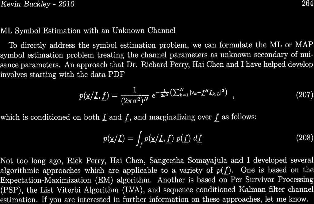
321
Detection and Estimation of Signals in Noise. Dr. Robert Schober Department of Electrical and Computer Engineering University of British Columbia
 Detection and Estimation of Signals in Noise Dr. Robert Schober Department of Electrical and Computer Engineering University of British Columbia Vancouver, August 24, 2010 2 Contents 1 Basic Elements
ECE 8771, Information Theory & Coding for Digital Communications Summer 2010 Syllabus & Outline (Draft 1 - May 12, 2010)
") ECE 8771, Information Theory & Coding for Digital Communications Summer 2010 Syllabus & Outline (Draft 1 - May 12, 2010) Instructor: Kevin Buckley, Tolentine 433a, 610-519-5658 (W), 610-519-4436 (F), buckley@ece.vill.edu,
ECE 8771, Information Theory & Coding for Digital Communications Summer 2010 Syllabus & Outline (Draft 1 - May 12, 2010) Instructor: Kevin Buckley, Tolentine 433a, 610-519-5658 (W), 610-519-4436 (F), buckley@ece.vill.edu,
Handout 13: Intersymbol Interference
 ENGG 2310-B: Principles of Communication Systems 2018 19 First Term Handout 13: Intersymbol Interference Instructor: Wing-Kin Ma November 19, 2018 Suggested Reading: Chapter 8 of Simon Haykin and Michael
QUESTION BANK SUBJECT: DIGITAL COMMUNICATION (15EC61)
") QUESTION BANK SUBJECT: DIGITAL COMMUNICATION (15EC61) Module 1 1. Explain Digital communication system with a neat block diagram. 2. What are the differences between digital and analog communication systems?
QUESTION BANK SUBJECT: DIGITAL COMMUNICATION (15EC61) Module 1 1. Explain Digital communication system with a neat block diagram. 2. What are the differences between digital and analog communication systems?
Theory of Telecommunications Networks
 Theory of Telecommunications Networks Anton Čižmár Ján Papaj Department of electronics and multimedia telecommunications CONTENTS Preface... 5 1 Introduction... 6 1.1 Mathematical models for communication
Chapter 2: Signal Representation
 Chapter 2: Signal Representation Aveek Dutta Assistant Professor Department of Electrical and Computer Engineering University at Albany Spring 2018 Images and equations adopted from: Digital Communications
Amplitude Frequency Phase
 Chapter 4 (part 2) Digital Modulation Techniques Chapter 4 (part 2) Overview Digital Modulation techniques (part 2) Bandpass data transmission Amplitude Shift Keying (ASK) Phase Shift Keying (PSK) Frequency
Chapter 4. Part 2(a) Digital Modulation Techniques
 Digital Modulation Techniques") Chapter 4 Part 2(a) Digital Modulation Techniques Overview Digital Modulation techniques Bandpass data transmission Amplitude Shift Keying (ASK) Phase Shift Keying (PSK) Frequency Shift Keying (FSK) Quadrature
Chapter 4 Part 2(a) Digital Modulation Techniques Overview Digital Modulation techniques Bandpass data transmission Amplitude Shift Keying (ASK) Phase Shift Keying (PSK) Frequency Shift Keying (FSK) Quadrature
Department of Electronics and Communication Engineering 1
 UNIT I SAMPLING AND QUANTIZATION Pulse Modulation 1. Explain in detail the generation of PWM and PPM signals (16) (M/J 2011) 2. Explain in detail the concept of PWM and PAM (16) (N/D 2012) 3. What is the
Digital Communication System
 Digital Communication System Purpose: communicate information at certain rate between geographically separated locations reliably (quality) Important point: rate, quality spectral bandwidth requirement
Handout 11: Digital Baseband Transmission
 ENGG 23-B: Principles of Communication Systems 27 8 First Term Handout : Digital Baseband Transmission Instructor: Wing-Kin Ma November 7, 27 Suggested Reading: Chapter 8 of Simon Haykin and Michael Moher,
Objectives. Presentation Outline. Digital Modulation Revision
 Digital Modulation Revision Professor Richard Harris Objectives To identify the key points from the lecture material presented in the Digital Modulation section of this paper. What is in the examination
SIGNALS AND SYSTEMS LABORATORY 13: Digital Communication
 SIGNALS AND SYSTEMS LABORATORY 13: Digital Communication INTRODUCTION Digital Communication refers to the transmission of binary, or digital, information over analog channels. In this laboratory you will
Mobile Radio Systems OPAM: Understanding OFDM and Spread Spectrum
 Mobile Radio Systems OPAM: Understanding OFDM and Spread Spectrum Klaus Witrisal witrisal@tugraz.at Signal Processing and Speech Communication Laboratory www.spsc.tugraz.at Graz University of Technology
Communication Channels
 Communication Channels wires (PCB trace or conductor on IC) optical fiber (attenuation 4dB/km) broadcast TV (50 kw transmit) voice telephone line (under -9 dbm or 110 µw) walkie-talkie: 500 mw, 467 MHz
DIGITAL COMMUNICATIONS SYSTEMS. MSc in Electronic Technologies and Communications
 DIGITAL COMMUNICATIONS SYSTEMS MSc in Electronic Technologies and Communications Bandpass binary signalling The common techniques of bandpass binary signalling are: - On-off keying (OOK), also known as
ECEn 665: Antennas and Propagation for Wireless Communications 131. s(t) = A c [1 + αm(t)] cos (ω c t) (9.27)
![ECEn 665: Antennas and Propagation for Wireless Communications 131. s(t) = A c [1 + αm(t)] cos (ω c t) (9.27)](/thumbs/88/116957690.jpg "ECEn 665: Antennas and Propagation for Wireless Communications 131. s(t) = A c [1 + αm(t)] cos (ω c t) (9.27)") ECEn 665: Antennas and Propagation for Wireless Communications 131 9. Modulation Modulation is a way to vary the amplitude and phase of a sinusoidal carrier waveform in order to transmit information. When
ECEn 665: Antennas and Propagation for Wireless Communications 131 9. Modulation Modulation is a way to vary the amplitude and phase of a sinusoidal carrier waveform in order to transmit information. When
Digital Communication System
 Digital Communication System Purpose: communicate information at required rate between geographically separated locations reliably (quality) Important point: rate, quality spectral bandwidth, power requirements
Digital modulation techniques
 Outline Introduction Signal, random variable, random process and spectra Analog modulation Analog to digital conversion Digital transmission through baseband channels Signal space representation Optimal
Lab 3.0. Pulse Shaping and Rayleigh Channel. Faculty of Information Engineering & Technology. The Communications Department
 Faculty of Information Engineering & Technology The Communications Department Course: Advanced Communication Lab [COMM 1005] Lab 3.0 Pulse Shaping and Rayleigh Channel 1 TABLE OF CONTENTS 2 Summary...
COMMUNICATION SYSTEMS
 COMMUNICATION SYSTEMS 4TH EDITION Simon Hayhin McMaster University JOHN WILEY & SONS, INC. Ш.! [ BACKGROUND AND PREVIEW 1. The Communication Process 1 2. Primary Communication Resources 3 3. Sources of
EITG05 Digital Communications
 Fourier transform EITG05 Digital Communications Lecture 4 Bandwidth of Transmitted Signals Michael Lentmaier Thursday, September 3, 08 X(f )F{x(t)} x(t) e jπ ft dt X Re (f )+jx Im (f ) X(f ) e jϕ(f ) x(t)f
UNIVERSITY OF CALIFORNIA College of Engineering Department of Electrical Engineering and Computer Sciences EECS 121 FINAL EXAM
 Name: UNIVERSIY OF CALIFORNIA College of Engineering Department of Electrical Engineering and Computer Sciences Professor David se EECS 121 FINAL EXAM 21 May 1997, 5:00-8:00 p.m. Please write answers on
ENGG2310-B Principles of Communication Systems Last Lecture
 ENGG2310-B Principles of Communication Systems Last Lecture Wing-Kin Ma Department of Electronic Engineering The Chinese University of Hong Kong, Hong Kong November 28 29, 2017 Recap on ISI model: y(t)
Chapter 6 Passband Data Transmission
 Chapter 6 Passband Data Transmission Passband Data Transmission concerns the Transmission of the Digital Data over the real Passband channel. 6.1 Introduction Categories of digital communications (ASK/PSK/FSK)
Exercises for chapter 2
 Exercises for chapter Digital Communications A baseband PAM system uses as receiver filter f(t) a matched filter, f(t) = g( t), having two choices for transmission filter g(t) g a (t) = ( ) { t Π =, t,
ECE 4600 Communication Systems
 ECE 4600 Communication Systems Dr. Bradley J. Bazuin Associate Professor Department of Electrical and Computer Engineering College of Engineering and Applied Sciences Course Topics Course Introduction
2.1 BASIC CONCEPTS Basic Operations on Signals Time Shifting. Figure 2.2 Time shifting of a signal. Time Reversal.
 1 2.1 BASIC CONCEPTS 2.1.1 Basic Operations on Signals Time Shifting. Figure 2.2 Time shifting of a signal. Time Reversal. 2 Time Scaling. Figure 2.4 Time scaling of a signal. 2.1.2 Classification of Signals
CHAPTER 4 SIGNAL SPACE. Xijun Wang
 CHAPTER 4 SIGNAL SPACE Xijun Wang WEEKLY READING 1. Goldsmith, Wireless Communications, Chapters 5 2. Gallager, Principles of Digital Communication, Chapter 5 2 DIGITAL MODULATION AND DEMODULATION n Digital
a) Abasebanddigitalcommunicationsystemhasthetransmitterfilterg(t) thatisshowninthe figure, and a matched filter at the receiver.
 Abasebanddigitalcommunicationsystemhasthetransmitterfilterg(t) thatisshowninthe figure, and a matched filter at the receiver.") DIGITAL COMMUNICATIONS PART A (Time: 60 minutes. Points 4/0) Last Name(s):........................................................ First (Middle) Name:.................................................
DIGITAL COMMUNICATIONS PART A (Time: 60 minutes. Points 4/0) Last Name(s):........................................................ First (Middle) Name:.................................................
Modulation and Coding Tradeoffs
 0 Modulation and Coding Tradeoffs Contents 1 1. Design Goals 2. Error Probability Plane 3. Nyquist Minimum Bandwidth 4. Shannon Hartley Capacity Theorem 5. Bandwidth Efficiency Plane 6. Modulation and
Fund. of Digital Communications Ch. 3: Digital Modulation
 Fund. of Digital Communications Ch. 3: Digital Modulation Klaus Witrisal witrisal@tugraz.at Signal Processing and Speech Communication Laboratory www.spsc.tugraz.at Graz University of Technology November
Mobile & Wireless Networking. Lecture 2: Wireless Transmission (2/2)
") 192620010 Mobile & Wireless Networking Lecture 2: Wireless Transmission (2/2) [Schiller, Section 2.6 & 2.7] [Reader Part 1: OFDM: An architecture for the fourth generation] Geert Heijenk Outline of Lecture
192620010 Mobile & Wireless Networking Lecture 2: Wireless Transmission (2/2) [Schiller, Section 2.6 & 2.7] [Reader Part 1: OFDM: An architecture for the fourth generation] Geert Heijenk Outline of Lecture
CSE4214 Digital Communications. Bandpass Modulation and Demodulation/Detection. Bandpass Modulation. Page 1
 CSE414 Digital Communications Chapter 4 Bandpass Modulation and Demodulation/Detection Bandpass Modulation Page 1 1 Bandpass Modulation n Baseband transmission is conducted at low frequencies n Passband
San José State University Department of Electrical Engineering EE 161, Digital Communication Systems, Spring 2018
 San José State University Department of Electrical Engineering EE 161, Digital Communication Systems, Spring 2018 Instructor: Robert Morelos-Zaragoza Office Location: ENGR 373 Telephone: (408) 924-3879
Fundamentals of Digital Communication
 Fundamentals of Digital Communication Network Infrastructures A.A. 2017/18 Digital communication system Analog Digital Input Signal Analog/ Digital Low Pass Filter Sampler Quantizer Source Encoder Channel
Lecture 10. Digital Modulation
 Digital Modulation Lecture 10 On-Off keying (OOK), or amplitude shift keying (ASK) Phase shift keying (PSK), particularly binary PSK (BPSK) Frequency shift keying Typical spectra Modulation/demodulation
QUESTION BANK EC 1351 DIGITAL COMMUNICATION YEAR / SEM : III / VI UNIT I- PULSE MODULATION PART-A (2 Marks) 1. What is the purpose of sample and hold
 1. What is the purpose of sample and hold") QUESTION BANK EC 1351 DIGITAL COMMUNICATION YEAR / SEM : III / VI UNIT I- PULSE MODULATION PART-A (2 Marks) 1. What is the purpose of sample and hold circuit 2. What is the difference between natural sampling
QUESTION BANK EC 1351 DIGITAL COMMUNICATION YEAR / SEM : III / VI UNIT I- PULSE MODULATION PART-A (2 Marks) 1. What is the purpose of sample and hold circuit 2. What is the difference between natural sampling
Outline Chapter 3: Principles of Digital Communications
 Outline Chapter 3: Principles of Digital Communications Structure of a Data Transmission System Up- and Down-Conversion Lowpass-to-Bandpass Conversion Baseband Presentation of Communication System Basic
UTA EE5362 PhD Diagnosis Exam (Spring 2012) Communications
 Communications") EE536 Spring 013 PhD Diagnosis Exam ID: UTA EE536 PhD Diagnosis Exam (Spring 01) Communications Instructions: Verify that your exam contains 11 pages (including the cover sheet). Some space is provided
EE536 Spring 013 PhD Diagnosis Exam ID: UTA EE536 PhD Diagnosis Exam (Spring 01) Communications Instructions: Verify that your exam contains 11 pages (including the cover sheet). Some space is provided
Problem Sheet 1 Probability, random processes, and noise
 Problem Sheet 1 Probability, random processes, and noise 1. If F X (x) is the distribution function of a random variable X and x 1 x 2, show that F X (x 1 ) F X (x 2 ). 2. Use the definition of the cumulative
Convolutional Coding Using Booth Algorithm For Application in Wireless Communication
 Available online at www.interscience.in Convolutional Coding Using Booth Algorithm For Application in Wireless Communication Sishir Kalita, Parismita Gogoi & Kandarpa Kumar Sarma Department of Electronics
Theory of Telecommunications Networks
 TT S KE M T Theory of Telecommunications Networks Anton Čižmár Ján Papaj Department of electronics and multimedia telecommunications CONTENTS Preface... 5 1 Introduction... 6 1.1 Mathematical models for
PRINCIPLES OF COMMUNICATIONS
 PRINCIPLES OF COMMUNICATIONS Systems, Modulation, and Noise SIXTH EDITION INTERNATIONAL STUDENT VERSION RODGER E. ZIEMER University of Colorado at Colorado Springs WILLIAM H. TRANTER Virginia Polytechnic
Problem Sheets: Communication Systems
 Problem Sheets: Communication Systems Professor A. Manikas Chair of Communications and Array Processing Department of Electrical & Electronic Engineering Imperial College London v.11 1 Topic: Introductory
Digital Modulators & Line Codes
 Digital Modulators & Line Codes Professor A. Manikas Imperial College London EE303 - Communication Systems An Overview of Fundamental Prof. A. Manikas (Imperial College) EE303: Dig. Mod. and Line Codes
Combined Transmitter Diversity and Multi-Level Modulation Techniques
 SETIT 2005 3rd International Conference: Sciences of Electronic, Technologies of Information and Telecommunications March 27 3, 2005 TUNISIA Combined Transmitter Diversity and Multi-Level Modulation Techniques
Wideband Channel Characterization. Spring 2017 ELE 492 FUNDAMENTALS OF WIRELESS COMMUNICATIONS 1
 Wideband Channel Characterization Spring 2017 ELE 492 FUNDAMENTALS OF WIRELESS COMMUNICATIONS 1 Wideband Systems - ISI Previous chapter considered CW (carrier-only) or narrow-band signals which do NOT
CALIFORNIA STATE UNIVERSITY, NORTHRIDGE FADING CHANNEL CHARACTERIZATION AND MODELING
 CALIFORNIA STATE UNIVERSITY, NORTHRIDGE FADING CHANNEL CHARACTERIZATION AND MODELING A graduate project submitted in partial fulfillment of the requirements For the degree of Master of Science in Electrical
Columbia University. Principles of Communication Systems ELEN E3701. Spring Semester May Final Examination
 1 Columbia University Principles of Communication Systems ELEN E3701 Spring Semester- 2006 9 May 2006 Final Examination Length of Examination- 3 hours Answer All Questions Good Luck!!! I. Kalet 2 Problem
Digital Communication Digital Modulation Schemes
 Digital Communication Digital Modulation Schemes Yabo Li Fall, 2013 Chapter Outline Representation of Digitally Modulated Signals Linear Modulation PAM PSK QAM Multi-Dimensional Signal Non-linear Modulation
Transmission Fundamentals
 College of Computer & Information Science Wireless Networks Northeastern University Lecture 1 Transmission Fundamentals Signals Data rate and bandwidth Nyquist sampling theorem Shannon capacity theorem
EE4601 Communication Systems
 EE4601 Communication Systems Week 1 Introduction to Digital Communications Channel Capacity 0 c 2015, Georgia Institute of Technology (lect1 1) Contact Information Office: Centergy 5138 Phone: 404 894
Theory of Telecommunications Networks
 Theory of Telecommunications Networks Anton Čižmár Ján Papaj Department of electronics and multimedia telecommunications CONTENTS Preface... 5 Introduction... 6. Mathematical models for communication channels...
Wireless PHY: Modulation and Demodulation
 Wireless PHY: Modulation and Demodulation Y. Richard Yang 09/11/2012 Outline Admin and recap Amplitude demodulation Digital modulation 2 Admin Assignment 1 posted 3 Recap: Modulation Objective o Frequency
EFFECTIVE CHANNEL CODING OF SERIALLY CONCATENATED ENCODERS AND CPM OVER AWGN AND RICIAN CHANNELS
 EFFECTIVE CHANNEL CODING OF SERIALLY CONCATENATED ENCODERS AND CPM OVER AWGN AND RICIAN CHANNELS Manjeet Singh (ms308@eng.cam.ac.uk) Ian J. Wassell (ijw24@eng.cam.ac.uk) Laboratory for Communications Engineering
Statistical Communication Theory
 Statistical Communication Theory Mark Reed 1 1 National ICT Australia, Australian National University 21st February 26 Topic Formal Description of course:this course provides a detailed study of fundamental
Principles of Communications
 Principles of Communications Meixia Tao Shanghai Jiao Tong University Chapter 8: Digital Modulation Techniques Textbook: Ch 8.4 8.5, Ch 10.1-10.5 1 Topics to be Covered data baseband Digital modulator
Chapter 2 Direct-Sequence Systems
 Chapter 2 Direct-Sequence Systems A spread-spectrum signal is one with an extra modulation that expands the signal bandwidth greatly beyond what is required by the underlying coded-data modulation. Spread-spectrum
PROJECT 5: DESIGNING A VOICE MODEM. Instructor: Amir Asif
 PROJECT 5: DESIGNING A VOICE MODEM Instructor: Amir Asif CSE4214: Digital Communications (Fall 2012) Computer Science and Engineering, York University 1. PURPOSE In this laboratory project, you will design
Chpater 8 Digital Transmission through Bandlimited AWGN Channels
 Chapter 8. Digital Transmission through Bandlimited AWGN Channels - 1-1 st Semester, 008 Chpater 8 Digital Transmission through Bandlimited AWGN Channels Text. [1] J. G. Proakis and M. Salehi, Communication
Wireless Communication Fading Modulation
 EC744 Wireless Communication Fall 2008 Mohamed Essam Khedr Department of Electronics and Communications Wireless Communication Fading Modulation Syllabus Tentatively Week 1 Week 2 Week 3 Week 4 Week 5
EXAMINATION FOR THE DEGREE OF B.E. Semester 1 June COMMUNICATIONS IV (ELEC ENG 4035)
") EXAMINATION FOR THE DEGREE OF B.E. Semester 1 June 2007 101902 COMMUNICATIONS IV (ELEC ENG 4035) Official Reading Time: Writing Time: Total Duration: 10 mins 120 mins 130 mins Instructions: This is a closed
EXAMINATION FOR THE DEGREE OF B.E. Semester 1 June 2007 101902 COMMUNICATIONS IV (ELEC ENG 4035) Official Reading Time: Writing Time: Total Duration: 10 mins 120 mins 130 mins Instructions: This is a closed
The University of Texas at Austin Dept. of Electrical and Computer Engineering Final Exam
 The University of Texas at Austin Dept. of Electrical and Computer Engineering Final Exam Date: December 18, 2017 Course: EE 313 Evans Name: Last, First The exam is scheduled to last three hours. Open
Chapter 9. Digital Communication Through Band-Limited Channels. Muris Sarajlic
 Chapter 9 Digital Communication Through Band-Limited Channels Muris Sarajlic Band limited channels (9.1) Analysis in previous chapters considered the channel bandwidth to be unbounded All physical channels
Outline. EECS 3213 Fall Sebastian Magierowski York University. Review Passband Modulation. Constellations ASK, FSK, PSK.
 EECS 3213 Fall 2014 L12: Modulation Sebastian Magierowski York University 1 Outline Review Passband Modulation ASK, FSK, PSK Constellations 2 1 Underlying Idea Attempting to send a sequence of digits through
Other Modulation Techniques - CAP, QAM, DMT
 Other Modulation Techniques - CAP, QAM, DMT Prof. David Johns (johns@eecg.toronto.edu) (www.eecg.toronto.edu/~johns) slide 1 of 47 Complex Signals Concept useful for describing a pair of real signals Let
Modern Quadrature Amplitude Modulation Principles and Applications for Fixed and Wireless Channels
 1 Modern Quadrature Amplitude Modulation Principles and Applications for Fixed and Wireless Channels W.T. Webb, L.Hanzo Contents PART I: Background to QAM 1 Introduction and Background 1 1.1 Modulation
Time division multiplexing The block diagram for TDM is illustrated as shown in the figure
 CHAPTER 2 Syllabus: 1) Pulse amplitude modulation 2) TDM 3) Wave form coding techniques 4) PCM 5) Quantization noise and SNR 6) Robust quantization Pulse amplitude modulation In pulse amplitude modulation,
ESE531 Spring University of Pennsylvania Department of Electrical and System Engineering Digital Signal Processing
 University of Pennsylvania Department of Electrical and System Engineering Digital Signal Processing ESE531, Spring 2017 Final Project: Audio Equalization Wednesday, Apr. 5 Due: Tuesday, April 25th, 11:59pm
Physical Layer: Modulation, FEC. Wireless Networks: Guevara Noubir. S2001, COM3525 Wireless Networks Lecture 3, 1
 Wireless Networks: Physical Layer: Modulation, FEC Guevara Noubir Noubir@ccsneuedu S, COM355 Wireless Networks Lecture 3, Lecture focus Modulation techniques Bit Error Rate Reducing the BER Forward Error
Thus there are three basic modulation techniques: 1) AMPLITUDE SHIFT KEYING 2) FREQUENCY SHIFT KEYING 3) PHASE SHIFT KEYING
 AMPLITUDE SHIFT KEYING 2) FREQUENCY SHIFT KEYING 3) PHASE SHIFT KEYING") CHAPTER 5 Syllabus 1) Digital modulation formats 2) Coherent binary modulation techniques 3) Coherent Quadrature modulation techniques 4) Non coherent binary modulation techniques. Digital modulation formats:
CHAPTER 5 Syllabus 1) Digital modulation formats 2) Coherent binary modulation techniques 3) Coherent Quadrature modulation techniques 4) Non coherent binary modulation techniques. Digital modulation formats:
Principles of Communications
 Principles of Communications Weiyao Lin Shanghai Jiao Tong University Chapter 8: Digital Modulation Techniques Textbook: Ch 8.4.8.7 2009/2010 Meixia Tao @ SJTU 1 Topics to be Covered data baseband Digital
MATLAB^/Simulink for Digital Communication
 /n- i-.1 MATLAB^/Simulink for Digital Communication Won Y. Yang, Yong S. Cho, Won G. Jeon, Jeong W. Lee, Jong H. Paik Jae K. Kim, Mi-Hyun Lee, Kyu I. Lee, Kyung W. Park, Kyung S. Woo V Table of j Contents
Handout 2: Fourier Transform
 ENGG 2310-B: Principles of Communication Systems Handout 2: Fourier ransform 2018 19 First erm Instructor: Wing-Kin Ma September 3, 2018 Suggested Reading: Chapter 2 of Simon Haykin and Michael Moher,
Lecture 3: Wireless Physical Layer: Modulation Techniques. Mythili Vutukuru CS 653 Spring 2014 Jan 13, Monday
 Lecture 3: Wireless Physical Layer: Modulation Techniques Mythili Vutukuru CS 653 Spring 2014 Jan 13, Monday Modulation We saw a simple example of amplitude modulation in the last lecture Modulation how
Course Specifications
 Development Cluster Computer and Networking Engineering (CNE) Cluster Lead Developer Amir Asif Module Names Module 1: Baseband and Bandpass Communications (40 characters or less Module 2: Channel Coding
Performance analysis of BPSK system with ZF & MMSE equalization
 Performance analysis of BPSK system with ZF & MMSE equalization Manish Kumar Department of Electronics and Communication Engineering Swift institute of Engineering & Technology, Rajpura, Punjab, India
Syllabus. osmania university UNIT - I UNIT - II UNIT - III CHAPTER - 1 : INTRODUCTION TO DIGITAL COMMUNICATION CHAPTER - 3 : INFORMATION THEORY
 i Syllabus osmania university UNIT - I CHAPTER - 1 : INTRODUCTION TO Elements of Digital Communication System, Comparison of Digital and Analog Communication Systems. CHAPTER - 2 : DIGITAL TRANSMISSION
Performance Evaluation of ½ Rate Convolution Coding with Different Modulation Techniques for DS-CDMA System over Rician Channel
 Performance Evaluation of ½ Rate Convolution Coding with Different Modulation Techniques for DS-CDMA System over Rician Channel Dilip Mandloi PG Scholar Department of ECE, IES, IPS Academy, Indore [India]
1.Explain the principle and characteristics of a matched filter. Hence derive the expression for its frequency response function.
 1.Explain the principle and characteristics of a matched filter. Hence derive the expression for its frequency response function. Matched-Filter Receiver: A network whose frequency-response function maximizes
PULSE SHAPING AND RECEIVE FILTERING
 PULSE SHAPING AND RECEIVE FILTERING Pulse and Pulse Amplitude Modulated Message Spectrum Eye Diagram Nyquist Pulses Matched Filtering Matched, Nyquist Transmit and Receive Filter Combination adaptive components
ECE5713 : Advanced Digital Communications
 ECE5713 : Advanced Digital Communications Bandpass Modulation MPSK MASK, OOK MFSK 04-May-15 Advanced Digital Communications, Spring-2015, Week-8 1 In-phase and Quadrature (I&Q) Representation Any bandpass
Communication Systems
 Electrical Engineering Communication Systems Comprehensive Theory with Solved Examples and Practice Questions Publications Publications MADE EASY Publications Corporate Office: 44-A/4, Kalu Sarai (Near
Objectives. Presentation Outline. Digital Modulation Lecture 03
 Digital Modulation Lecture 03 Inter-Symbol Interference Power Spectral Density Richard Harris Objectives To be able to discuss Inter-Symbol Interference (ISI), its causes and possible remedies. To be able
Lecture 2 Review of Signals and Systems: Part 1. EE4900/EE6720 Digital Communications
 EE4900/EE6420: Digital Communications 1 Lecture 2 Review of Signals and Systems: Part 1 Block Diagrams of Communication System Digital Communication System 2 Informatio n (sound, video, text, data, ) Transducer
Principles of Baseband Digital Data Transmission
 Principles of Baseband Digital Data Transmission Prof. Wangrok Oh Dept. of Information Communications Eng. Chungnam National University Prof. Wangrok Oh(CNU) / 3 Overview Baseband Digital Data Transmission
Lecture 13. Introduction to OFDM
 Lecture 13 Introduction to OFDM Ref: About-OFDM.pdf Orthogonal frequency division multiplexing (OFDM) is well-known to be effective against multipath distortion. It is a multicarrier communication scheme,
ELT Receiver Architectures and Signal Processing Fall Mandatory homework exercises
 ELT-44006 Receiver Architectures and Signal Processing Fall 2014 1 Mandatory homework exercises - Individual solutions to be returned to Markku Renfors by email or in paper format. - Solutions are expected
COMM 601: Modulation I
 Prof. Ahmed El-Mahdy, Communications Department The German University in Cairo Text Books [1] Couch, Digital and Analog Communication Systems, 7 th edition, Prentice Hall, 2007. [2] Simon Haykin, Communication
UNIT I Source Coding Systems
 SIDDHARTH GROUP OF INSTITUTIONS: PUTTUR Siddharth Nagar, Narayanavanam Road 517583 QUESTION BANK (DESCRIPTIVE) Subject with Code: DC (16EC421) Year & Sem: III-B. Tech & II-Sem Course & Branch: B. Tech
Exam in 1TT850, 1E275. Modulation, Demodulation and Coding course
 Exam in 1TT850, 1E275 Modulation, Demodulation and Coding course EI, TF, IT programs 16th of August 2004, 14:00-19:00 Signals and systems, Uppsala university Examiner Sorour Falahati office: 018-471 3071
Wireless Communication: Concepts, Techniques, and Models. Hongwei Zhang
 Wireless Communication: Concepts, Techniques, and Models Hongwei Zhang http://www.cs.wayne.edu/~hzhang Outline Digital communication over radio channels Channel capacity MIMO: diversity and parallel channels
COHERENT DEMODULATION OF CONTINUOUS PHASE BINARY FSK SIGNALS
 COHERENT DEMODULATION OF CONTINUOUS PHASE BINARY FSK SIGNALS M. G. PELCHAT, R. C. DAVIS, and M. B. LUNTZ Radiation Incorporated Melbourne, Florida 32901 Summary This paper gives achievable bounds for the
ELEC 7073 Digital Communication III
 ELEC 7073 Digital Communication III Lecturers: Dr. S. D. Ma and Dr. Y. Q. Zhou (sdma@eee.hku.hk; yqzhou@eee.hku.hk) Date & Time: Tuesday: 7:00-9:30pm Place: CYC Lecture Room A Notes can be obtained from:
QUESTION BANK. Staff In-Charge: M.MAHARAJA, AP / ECE
 FATIMA MICHAEL COLLEGE OF ENGINEERING & TECHNOLOGY Senkottai Village, Madurai Sivagangai Main Road, Madurai -625 020 An ISO 9001:2008 Certified Institution QUESTION BANK Sub. Code : EC 2301 Class : III
Communication Systems
 Electronics Engineering Communication Systems Comprehensive Theory with Solved Examples and Practice Questions Publications Publications MADE EASY Publications Corporate Office: 44-A/4, Kalu Sarai (Near
Implementation of Different Interleaving Techniques for Performance Evaluation of CDMA System
 Implementation of Different Interleaving Techniques for Performance Evaluation of CDMA System Anshu Aggarwal 1 and Vikas Mittal 2 1 Anshu Aggarwal is student of M.Tech. in the Department of Electronics
HW 6 Due: November 3, 10:39 AM (in class)
") ECS 332: Principles of Communications 2015/1 HW 6 Due: November 3, 10:39 AM (in class) Lecturer: Prapun Suksompong, Ph.D. Instructions (a) ONE part of a question will be graded (5 pt). Of course, you do
ECS 332: Principles of Communications 2015/1 HW 6 Due: November 3, 10:39 AM (in class) Lecturer: Prapun Suksompong, Ph.D. Instructions (a) ONE part of a question will be graded (5 pt). Of course, you do
CHANNEL ENCODING & DECODING. Binary Interface
 CHANNEL ENCODING & DECODING Input Source Encoder Channel Encoder Binary Interface Channel Output Source Decoder Channel Decoder 1 Simplest Example of channel encoding A sequence of binary digits is mapped,