Optically read displacement detection using phase modulated diffraction gratings with reduced zeroth order reflections
|
|
|
- Kristina Cox
- 5 years ago
- Views:
Transcription
1 Submitted to Applied Physics Letters: (Revised and resubmitted: ) Optically read displacement detection using phase modulated diffraction gratings with reduced zeroth order reflections Randall P. Williams, Samuel K. Hord, and Neal A. Hall a Department of Electrical and Computer Engineering, The University of Texas at Austin, Austin, Texas 78712, USA a) Electronic mail: nahall@mail.utexas.edu Abstract: Displacement detection using optical interferometric techniques allows for low minimum detectable displacements which are unmatched by other displacement measurement methods as device sizes are scaled down. The use of diffractive optical elements as beam splitters has proven an effective way to realize miniature and robust optical interferometers. Diffraction gratings commonly used in such applications, however, can generate a zeroth order reflected beam which results in reduced sensor performance, packaging limitations, and laser instability. A diffraction grating concept has been designed, fabricated, and tested which has the effect of reducing the zeroth order component by imparting a half wavelength phase shift to a portion of the reflected light. The design criteria for zeroth order beam elimination is illustrated using a simple model based on phasor arithmetic. The microfabrication process used to prototype gratings is presented, and experimental measurements collected from the prototype are reported. The minimum detectable displacement achievable in sensor applications is found to be 3.6 fm/ Hz, which is comparable to sensors built using more conventional gratings. Finally, comparisons are made between the test results and the simple model predictions. 1
2 The ability to detect small changes in displacement is central to the operation of many vibration sensors such as microphones and accelerometers. In a microphone, for instance, incident acoustic pressure causes a diaphragm or membrane to deflect 1, and knowledge of the displacement can be used to find the amplitude of the incident pressure. In an accelerometer, a proof mass is mechanically suspended from the frame of the sensor, and an applied acceleration causes relative displacement between the proof mass and the supporting structure 2. Measuring this displacement may be used in turn to find the applied acceleration. While small sensors fabricated using microelectromechanical systems (MEMS) techniques frequently employ of capacitive schemes for sensing displacement, scaling laws show that reducing the mechanical footprint of the capacitive sensors results in decreased signal to noise (SNR) 3. Optical displacement detection schemes, on the other hand, are not subject to the same scaling laws as capacitive methods, and provide an attractive alternative detection mechanism for MEMS sensors. The use of deformable lamellar gratings for modulating infrared beams was first demonstrated in the late 1950s 4 for use in an interferometer. Solgaard et al. first demonstrated a MEMS optical modulator based on the same modulation principle with electrostatic actuation 5, which then found widespread incorporation into a variety of opticallyread MEMS sensors. Published examples of such grating based devices include capacitive micromachined ultrasonic transducers (cmuts) 6, microphones 7 10, accelerometers 11 14, infrared detector arrays 15, and atomic force microscope applications 16,17, in addition to other non sensor MEMS devices such as light valves for use in switching and projection applications 18. 2
3 A schematic diagram of a grating based interferometric optical accelerometer is shown in Figure 1. A proof mass with an optically reflective bottom surface is suspended above a stationary diffraction grating and moves in response to applied acceleration. A coherent light source, such as a vertical cavity surface emitting laser (VCSEL), is incident from the bottom of the structure. A portion of the light is directly reflected from the diffraction grating fingers while the remainder of the light is reflected from the proof mass, accruing an additional phase shift equal to 2 before leaving the cavity. The phase difference between the light reflected from the grating fingers and that from the proof mass results in an interference pattern, appearing as a set of diffracted beams, or diffraction orders. The grating equation gives the departure angle,, of the th order beam as sin /, where is the order number, is the wavelength of incident light, and is the pitch of the grating 19. The intensity of one order relative to the incident optical intensity is the diffraction efficiency, which is modulated with the reflector displacement, and measurement of this intensity using photodetectors (PDs) allows for determination of the reflector displacement. 3

4 Figure 1: Schematic illustration of an optical interferometric accelerometer highlighting critical system components While the optical system described above is straightforward in principle, positioning and integration of the optoelectronic components in a compact MEMS implementation presents multiple challenges. The light emitted from most VCSELs is highly divergent, typically at least several degrees full width at half maximum (FWHM), so a lens to collimate the light incident on the grating helps to maximize interferometric sensitivity. Additionally, VCSELs and other semiconductor lasers can be extremely sensitive to feedback from light reflected back into the laser cavity, which causes instabilities 20. The reflection of the 0 th order beam back into the laser cavity is therefore to be avoided 3. One method of eliminating back reflections into the laser cavity is to position the incident beam at a small angle relative to the grating surface, such that the 0 th order beam is reflected away 4
5 from the laser aperture 3. This allows the 0 th order beam to be entirely captured by a photodetector for sensing purposes. However, non normal incidence complicates MEMS packaging, since the beam from a VCSEL is emitted normal to the die surface. A strong motivation exists to explore a grating design that eliminates zero order beam generation, thereby enabling robust, surface normal integrated optically read MEMS. An advanced diffraction grating has been conceptualized and is discussed here, which has the effect of reducing the zeroth order reflected beam via destructive interference of light emitted from out of phase regions. Using varying phase shifts to control the behavior of the light diffracted by interdigitated reflection gratings has already been demonstrated for grating light valves, by dynamically adjusting the position of each mobile grating finger to vary the optical path distance 21 23, or by depositing an optical coating of varying thickness on top of the reflecting fingers Interdigitated gratings are not suitable for certain applications such as microphones, due to air leakage through the gaps between the fingers. Additionally, controlling the phase shift of each reflecting finger via position adjustments requires actuation and control over the finger position, while in a sensor application the finger position changes in response to some external stimulus and is to be detected rather than controlled. These considerations therefore motivate the use of a continuous, rigid grating incorporating both reflecting and transmitting regions, backed by a planar mirror. While devices incorporating two adjacent binary gratings each having different phase shifts have been reported in the literature 16 for the purposes of tailoring the diffracted order behavior, this embodiment directly interleaves the out of phase regions into a single periodic grating. 5
 of equal width: two reflecting regions at different heights, and two transmitting")
6 A schematic illustration of the conceptualized grating is presented in Figure 2. In contrast to a standard Ronchi type binary grating, this grating consists of four distinct regions ( fingers ) of equal width: two reflecting regions at different heights, and two transmitting regions of different height. Figure 2: Geometry of the four region diffraction grating used to eliminate 0th order diffracted beam. Three periods are shown. The ideal far field intensity of the 0 th order beam and the criteria for its elimination may be determined using a simple phasor model rooted in Huygens principle 27, considering each grating region as an independent wavelet source of equal magnitude but varying phase determined by the optical distance traveled by the light as it traverses the grating. A complex phasor exp can be used to represent the light reflected from the th region, as shown in Figure 3(a), where is the phase of the wavelet, and the vector sum over the four regions gives the zeroth order amplitude. Choosing the region thicknesses such that phasors and are 180 out of phase with each other, and similarly choosing thicknesses such that and are 180 degrees out of phase with each other, assures that, for any distance between the grating and proof mass, destructive interference results in the elimination of the 0 th order output beam. Figure 3(b) provides a geometric representation of the phasors on the complex 6
 where is the wavelength of incident light in air and is the index of refraction in the transparent substrate.")
7 unit circle for this condition of no zeroth order reflection. This requires the dimensions and to be: 4 Eq. (1) and 4 1, Eq. (2) where is the wavelength of incident light in air and is the index of refraction in the transparent substrate. Figure 3: Wavelet phasors corresponding to each of the four grating regions (a) and geometric representation of phasors in the complex plane (b) The phase difference between phasors and is dependent on the reflector distance and determines the intensity of the non zero diffraction orders. The far field diffraction pattern may be found from scalar diffraction theory 28 and can be used to determine the intensities of 7
8 the higher order diffraction beams and their modulation behavior as a function of reflector displacement. The complex amplitude of the light leaving the diffraction grating is expressed as a piecewise periodic function, having unit magnitude and varying phase,. Referring to Figure 3, light reflected from the reflectors has phase independent of, while light returned from the moving reflector has a phase proportional to. The phase of the first region,, can be taken as the zero reference without loss of generality. In the Fraunhofer approximation for scalar diffraction, taking the spatial Fourier transform of and setting the wavenumber in the direction to sin gives the far field distribution of the optical disturbance, and squaring the modulus gives the far field intensity. The intensity of the 0 th order beam is found to be zero, and the intensities of the +1 and 1 orders, normalized by the incident intensity, are found to be: 4 1 sin 4 Eq. (3) 4 1 sin 4 Eq. (4) Figure 4 shows the intensities of the +1 and 1 diffraction orders as functions of reflector displacement given in Eq. (3) Eq. (4). The modulation of the orders is periodic in displacement increments of /2, similar to the behavior of a Michelson type interferometer. The +1 and 1 beams are complementary, being 180 out of phase with equal magnitude, allowing for differential measurement which reduces the effects of common mode error sources such as laser relative intensity noise (RIN) 3 and PD dark current. 8
9 Figure 4: Diffraction efficiency for the three center orders as a function of normalized grating to reflector distance The four region stepped grating was prototyped on a double side polished fused silica (SiO 2 ) wafer using typical microfabrication techniques. While conventional binary reflecting gratings may be patterned on a flat substrate in a single photolithography step, achieving four regions with different phase shifts required three etch steps to provide the thickness variation. A schematic illustration of the fabrication flow used is shown in Figure 5. In order to ensure proper alignment between the Cr/Cr 2 O 3 reflectors and the etched trenches, a single photoresist (PR) mask was used for both the etch mask in step 3 and for patterning the thin film deposited in step 4. Finally, the deposited Cr/Cr 2 O 3 regions were used to form the edges of the last etch mask, increasing the alignment tolerance needed during the final photolithography step from nominally 0.1 μm to 0.5 μm. 9

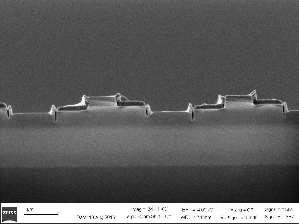
10 Figure 5: Fabrication process steps used to prototype the four region advanced diffraction gratings A scanning electron micrograph of the prototype grating cross section is seen in Figure 6. The four different regions of each period are clearly visible, although the widths of the regions are not exactly equal due to variability of the photolithography process. Also seen on this prototype is a small crack near the lower edge of each Cr/Cr 2 O 3 reflector due to in plane residual stresses. 10

11 Figure 6: Scanning electron micrograph of completed grating cross section Microfabricated gratings were tested experimentally to capture the modulation behavior of the diffraction orders as a function of grating to mirror displacement. The test apparatus used to control the displacement consisted of a modified moving coil electromagnetic actuator, 32 mm wide and 36mm tall, an 850 nm collimated VCSEL, and a charge coupled device (CCD) optical detector (IDS Imaging model UI 1540LE M GL), illustrated in Figure 7. A gold coated square mirror, 2.3 mm x 2.3 mm in size was affixed to the top of the stationary permanent magnet structure, and the 3.0 mm x 2.0mm grating prototype was mounted parallel to it on the coil bobbin. The motor structure was designed to provide a displacement proportional to current over the target travel range. The laser source was focused near the grating surface using an aspheric lens at an incidence angle of 2 from surface normal using a small steering mirror, and the beams diffracted away from the grating were then incident on the CCD. The test apparatus was mounted on a vibration isolation table from Minus K Technologies to reduce the noise due to ambient vibrations to within a fraction of an interference cycle. 11

12 Figure 7: Schematic diagram of experimental test apparatus used. A moving coil motor is used to displace the grating relative to a stationary mirror, while light is incident from an 850 nm VCSEL and a detector captures the intensity of the diffracted beams. The power emitted by the VCSEL was measured as 2.7 μw using a Thorlabs PM120VA laser power meter at the beginning and end of the experiment. To calibrate the CCD output to the optical beam power, several frames of CCD data were first collected with the laser source off in order to determine the dark current of the device, which was subtracted from subsequent readings. The laser was then directly incident on the CCD, and the intensity distribution was captured in order to correlate the numerical pixel values to the beam power. To measure the diffraction properties of the grating, the beam was focused near the grating surface and a National Instruments NI 9263 digital to analog converter and Texas Instruments OPA2140 amplifier were used to drive the motor coil with a linearly increasing current, until the grating was brought into contact with the stationary mirror, while simultaneously capturing the output field with the CCD. The CCD returns the 2D optical field in the observation plane, so the 12
13 intensity was then integrated over each beam to find the optical power of each as a function of reflector displacement, and was passed through a low pass filter to reduce the effect of background vibration. Figure 8 presents the optical power in each of the center three diffracted beams, normalized by the incident beam power, over a one wavelength displacement range when the reflector and mirror are nearly touching. These measurements are in qualitatively good agreement with the key model predictions shown previously in Figure 4: (i) the +1 and 1 orders are out of phase and nearly complementary, as expected, and (ii) the 0 order beam power is greatly reduced and is dominated by a DC component. While the ideal diffraction model predicts 100% modulation of the first orders and complete elimination of the zeroth order, several non ideal effects such as spurious reflections from the flat side of the substrate, diffraction between the grating and mirror, and fabrication and alignment tolerances likely account for these discrepancies and will be the subject of future investigations. Figure 8: Power in the center three diffracted beams as a function of mirror displacement 13
14 The experimental data can be used to determine the sensitivity of PD photocurrent to displacement and the minimum detectable displacement (MDD) of the interferometer when used in vibration measurement applications, with details of the calculations given by W. Lee, et al. 7. For an 850 nm laser source emitting 1 mw of optical power, PD responsivity of 0.5 A/W, and measuring the difference between the +1 and 1 responses, the experimental data yields a peak sensitivity of / = 2.4 µa/nm. The PD shot noise limit is found to be 8.6 pa/ Hz, yielding a sensor MDD of 3.6 fm/ Hz in a 1 Hz band. Multiplying by the square root of an application s required bandwidth then yields the application specific MDD. In comparison, sensors using conventional gratings published in the literature, MDD values as low as 20 fm/ Hz have been reported 29. This serves to show that through proper design of the diffraction grating elements, the behavior of the different diffracted beams can be tailored to specific sensing applications while matching or exceeding the low input referred noise of sensors using conventional gratings, which will ultimately facilitate packaging of such optoelectronic systems into MEMS devices. Acknowledgements The authors would like to thank the Office of Naval Research for funding this project under award number N The authors would also like to thank Brad Avenson and Claudia Villalobos for their assistance in assembling the test apparatus, and Moinuddin Ahmed for helpful discussions regarding the microfabrication process. References 14
15 1 J. Fraden, Handbook of modern sensors: physics, designs, and applications. (Springer Science & Business Media, New York, NY, 2004). 2 T. G. Beckwith, R. D. Marangoni, and J. H. Lienhard, Mechanical measurements. (Addison Wesley, Reading, MA, 1995). 3 M. L. Kuntzman, C. T. Garcia, A. G. Onaran, B. Avenson, K. D. Kirk, and N. A. Hall, Microelectromechanical Systems, Journal of 20, 828 (2011) J. Strong and G. A. Vanasse, J. Opt. Soc. Am. 50, 113 (1960). O. Solgaard, F. S. A. Sandejas, and D. M. Bloom, Opt. Lett. 17, 688 (1992). N. A. Hall, L. Wook, and F. Degertekin, Ultrasonics, Ferroelectrics, and Frequency Control, IEEE Transactions on 50, 1570 (2003). 7 W. Lee, N. A. Hall, Z. Zhou, and F. L. Degertekin, Selected Topics in Quantum Electronics, IEEE Journal of 10, 643 (2004). 8 9 K. Suzuki, H. Funaki, and Y. Naruse, Japanese Journal of Applied Physics 44, 3049 (2005). R. N. Miles, Q. Su, W. Cui, M. Shetye, F. L. Degertekin, B. Bicen, C. Garcia, S. Jones, and N. Hall, The Journal of the Acoustical Society of America 125, 2013 (2009). 10 K. Donghwan, C. T. Garcia, B. Avenson, and N. A. Hall, Microelectromechanical Systems, Journal of 23, 1101 (2014). 11 N. A. Hall, M. Okandan, R. Littrell, D. K. Serkland, G. A. Keeler, K. Peterson, B. Bicen, C. T. Garcia, and F. L. Degertekin, Microelectromechanical Systems, Journal of 17, 37 (2008). 12 C. T. Garcia, G. Onaran, B. Avenson, M. R. Christensen, Z. Liu, N. Hewa Kasakarage, and N. A. Hall, in Proceedings of the 2011 Monitoring Research Review: Ground Based Nuclear Explosion Monitoring Technologies (Tuscon, AZ, 2011), p
16 13 14 N. C. Loh, M. A. Schmidt, and S. R. Manalis, J Microelectromech S 11, 182 (2002). U. Krishnamoorthy, R. H. Olsson III, G. R. Bogart, M. S. Baker, D. W. Carr, T. P. Swiler, and P. J. Clews, Sensors and Actuators A: Physical , 283 (2008). 15 M. F. Toy, O. Ferhanoglu, H. Torun, and H. Urey, Sensors and Actuators A: Physical 156, 88 (2009) B. Van Gorp, A. G. Onaran, and F. L. Degertekin, Appl Phys Lett 91, (2007). G. G. Yaralioglu, A. Atalar, S. R. Manalis, and C. F. Quate, Journal of Applied Physics 83, 7405 (1998). 18 D. M. Bloom, in Proc. SPIE 3013: Projection Displays III, edited by Ming H. Wu (SPIE, San Jose, CA, 1997), pp E. Hecht, Optics, Third ed. (Addison Wesley, Reading, MA, 1998). A. E. Siegman, Lasers. (University Science Books, Mill Valley, California, 1986). A. A. Godil and D. M. Bloom, US Patent No. US B1 (July 31, 2001). M. W. Kowarz and B. E. Kruschwitz, Patent No. US B1 (January 9, 2001). N. Pilossof, United States of America Patent No. US B2 (September 9, 2003). J. C. Brazas Jr, M. W. Kowarz, and B. E. Kruschwitz, US Patent No. US 6,181,458 B1 (January 30, 2001). 25 D. T. Amm, J. Trisnadi, J. Hunter, C. Gudeman, and D. Maheshwari, US Patent No. US B2 (December 7, 2004). 26 H. Sagberg, M. Lacolle, I. R. Johansen, O. Løvhaugen, R. Belikov, O. Solgaard, and A. S. Sudbø, IEEE Journal of Selected Topics in Quantum Electronics 10, 604 (2004). 16
17 27 M. d. M. Sánchez López, I. Moreno, and A. Martínez García, in Proc. SPIE 11th Education and Training in Optics and Photonics Conference, edited by K. Alan Shore and Deb Kane (Optical Society of America, St. Asaph, United Kingdom, 2009), Vol. 9666, p E1. 28 J. W. Goodman, Introduction to Fourier optics, Third ed. (Roberts & Company, Englewood, CO, 2005). 29 N. A. Hall, M. Okandan, R. Littrell, B. Bicen, and F. L. Degertekin, The Journal of the Acoustical Society of America 122, 2031 (2007). 17
18
19
20
21
22
23
24
25
MICROMACHINED INTERFEROMETER FOR MEMS METROLOGY
 MICROMACHINED INTERFEROMETER FOR MEMS METROLOGY Byungki Kim, H. Ali Razavi, F. Levent Degertekin, Thomas R. Kurfess G.W. Woodruff School of Mechanical Engineering, Georgia Institute of Technology, Atlanta,
Sensitivity Enhancement of Bimaterial MOEMS Thermal Imaging Sensor Array using 2-λ readout
 Sensitivity Enhancement of Bimaterial MOEMS Thermal Imaging Sensor Array using -λ readout O. Ferhanoğlu, H. Urey Koç University, Electrical Engineering, Istanbul-TURKEY ABSTRACT Diffraction gratings integrated
A novel tunable diode laser using volume holographic gratings
 A novel tunable diode laser using volume holographic gratings Christophe Moser *, Lawrence Ho and Frank Havermeyer Ondax, Inc. 85 E. Duarte Road, Monrovia, CA 9116, USA ABSTRACT We have developed a self-aligned
BMC s heritage deformable mirror technology that uses hysteresis free electrostatic
 Optical Modulator Technical Whitepaper MEMS Optical Modulator Technology Overview The BMC MEMS Optical Modulator, shown in Figure 1, was designed for use in free space optical communication systems. The
Use of Computer Generated Holograms for Testing Aspheric Optics
 Use of Computer Generated Holograms for Testing Aspheric Optics James H. Burge and James C. Wyant Optical Sciences Center, University of Arizona, Tucson, AZ 85721 http://www.optics.arizona.edu/jcwyant,
Design and Analysis of Resonant Leaky-mode Broadband Reflectors
 846 PIERS Proceedings, Cambridge, USA, July 6, 8 Design and Analysis of Resonant Leaky-mode Broadband Reflectors M. Shokooh-Saremi and R. Magnusson Department of Electrical and Computer Engineering, University
MICROMACHINED BROADBAND ACOUSTIC TRANSDUCERS WITH INTEGRATED OPTICAL DISPLACEMENT DETECTION. A Dissertation Presented to. The Academic Faculty
 MICROMACHINED BROADBAND ACOUSTIC TRANSDUCERS WITH INTEGRATED OPTICAL DISPLACEMENT DETECTION A Dissertation Presented to The Academic Faculty By Neal A. Hall In Partial Fulfillment of the Requirements for
High-speed wavefront control using MEMS micromirrors T. G. Bifano and J. B. Stewart, Boston University [ ] Introduction
![High-speed wavefront control using MEMS micromirrors T. G. Bifano and J. B. Stewart, Boston University [ ] Introduction](/thumbs/72/66548311.jpg "High-speed wavefront control using MEMS micromirrors T. G. Bifano and J. B. Stewart, Boston University [ ] Introduction") High-speed wavefront control using MEMS micromirrors T. G. Bifano and J. B. Stewart, Boston University [5895-27] Introduction Various deformable mirrors for high-speed wavefront control have been demonstrated
High-speed wavefront control using MEMS micromirrors T. G. Bifano and J. B. Stewart, Boston University [5895-27] Introduction Various deformable mirrors for high-speed wavefront control have been demonstrated
IST IP NOBEL "Next generation Optical network for Broadband European Leadership"
 DBR Tunable Lasers A variation of the DFB laser is the distributed Bragg reflector (DBR) laser. It operates in a similar manner except that the grating, instead of being etched into the gain medium, is
Optical MEMS pressure sensor based on a mesa-diaphragm structure
 Optical MEMS pressure sensor based on a mesa-diaphragm structure Yixian Ge, Ming WanJ *, and Haitao Yan Jiangsu Key Lab on Opto-Electronic Technology, School of Physical Science and Technology, Nanjing
A MEMS Based Visible-NIR Fourier Transform Microspectrometer
 A MEMS Based Visible-NIR Fourier Transform Microspectrometer C. Ataman 1, H. Urey 1, S.O. Isikman 1, and A. Wolter 2 1 Optical Microsystems Laboratory, Department of Electrical Engineering, Koc University
Silicon Light Machines Patents
 820 Kifer Road, Sunnyvale, CA 94086 Tel. 408-240-4700 Fax 408-456-0708 www.siliconlight.com Silicon Light Machines Patents USPTO No. US 5,808,797 US 5,841,579 US 5,798,743 US 5,661,592 US 5,629,801 US
Multiply Resonant EOM for the LIGO 40-meter Interferometer
 LASER INTERFEROMETER GRAVITATIONAL WAVE OBSERVATORY - LIGO - CALIFORNIA INSTITUTE OF TECHNOLOGY MASSACHUSETTS INSTITUTE OF TECHNOLOGY LIGO-XXXXXXX-XX-X Date: 2009/09/25 Multiply Resonant EOM for the LIGO
Laser Telemetric System (Metrology)
") Laser Telemetric System (Metrology) Laser telemetric system is a non-contact gauge that measures with a collimated laser beam (Refer Fig. 10.26). It measure at the rate of 150 scans per second. It basically
Laser Telemetric System (Metrology) Laser telemetric system is a non-contact gauge that measures with a collimated laser beam (Refer Fig. 10.26). It measure at the rate of 150 scans per second. It basically
CHAPTER 5 FINE-TUNING OF AN ECDL WITH AN INTRACAVITY LIQUID CRYSTAL ELEMENT
 CHAPTER 5 FINE-TUNING OF AN ECDL WITH AN INTRACAVITY LIQUID CRYSTAL ELEMENT In this chapter, the experimental results for fine-tuning of the laser wavelength with an intracavity liquid crystal element
MEMS for RF, Micro Optics and Scanning Probe Nanotechnology Applications
 MEMS for RF, Micro Optics and Scanning Probe Nanotechnology Applications Part I: RF Applications Introductions and Motivations What are RF MEMS? Example Devices RFIC RFIC consists of Active components
Grating Light Valve and Vehicle Displays D. Corbin, D.T. Amm and R. W. Corrigan Silicon Light Machines, Sunnyvale, CA
 Grating Light Valve and Vehicle Displays D. Corbin, D.T. Amm and R. W. Corrigan Silicon Light Machines, Sunnyvale, CA Abstract The Grating Light Valve (GLV ) technology offers a unique combination of low
Lithography. 3 rd. lecture: introduction. Prof. Yosi Shacham-Diamand. Fall 2004
 Lithography 3 rd lecture: introduction Prof. Yosi Shacham-Diamand Fall 2004 1 List of content Fundamental principles Characteristics parameters Exposure systems 2 Fundamental principles Aerial Image Exposure
NEW LASER ULTRASONIC INTERFEROMETER FOR INDUSTRIAL APPLICATIONS B.Pouet and S.Breugnot Bossa Nova Technologies; Venice, CA, USA
 NEW LASER ULTRASONIC INTERFEROMETER FOR INDUSTRIAL APPLICATIONS B.Pouet and S.Breugnot Bossa Nova Technologies; Venice, CA, USA Abstract: A novel interferometric scheme for detection of ultrasound is presented.
D.C. Emmony, M.W. Godfrey and R.G. White
 A MINIATURE OPTICAL ACOUSTIC EMISSION TRANSDUCER ABSTRACT D.C. Emmony, M.W. Godfrey and R.G. White Department of Physics Loughborough University of Technology Loughborough, Leicestershire LEll 3TU United
Micro-sensors - what happens when you make "classical" devices "small": MEMS devices and integrated bolometric IR detectors
 Micro-sensors - what happens when you make "classical" devices "small": MEMS devices and integrated bolometric IR detectors Dean P. Neikirk 1 MURI bio-ir sensors kick-off 6/16/98 Where are the targets
Silicon on Insulator CMOS and Microelectromechanical Systems: Mechanical Devices, Sensing Techniques and System Electronics
 Silicon on Insulator CMOS and Microelectromechanical Systems: Mechanical Devices, Sensing Techniques and System Electronics Dissertation Defense Francisco Tejada Research Advisor A.G. Andreou Department
Project Staff: Timothy A. Savas, Michael E. Walsh, Thomas B. O'Reilly, Dr. Mark L. Schattenburg, and Professor Henry I. Smith
 9. Interference Lithography Sponsors: National Science Foundation, DMR-0210321; Dupont Agreement 12/10/99 Project Staff: Timothy A. Savas, Michael E. Walsh, Thomas B. O'Reilly, Dr. Mark L. Schattenburg,
High Sensitivity Interferometric Detection of Partial Discharges for High Power Transformer Applications
 High Sensitivity Interferometric Detection of Partial Discharges for High Power Transformer Applications Carlos Macià-Sanahuja and Horacio Lamela-Rivera Optoelectronics and Laser Technology group, Universidad
Deformable MEMS Micromirror Array for Wavelength and Angle Insensitive Retro-Reflecting Modulators Trevor K. Chan & Joseph E. Ford
 Photonics Systems Integration Lab UCSD Jacobs School of Engineering Deformable MEMS Micromirror Array for Wavelength and Angle Insensitive Retro-Reflecting Modulators Trevor K. Chan & Joseph E. Ford PHOTONIC
Fiber-optic Michelson Interferometer Sensor Fabricated by Femtosecond Lasers
 Sensors & ransducers 2013 by IFSA http://www.sensorsportal.com Fiber-optic Michelson Interferometer Sensor Fabricated by Femtosecond Lasers Dong LIU, Ying XIE, Gui XIN, Zheng-Ying LI School of Information
Analysis of phase sensitivity for binary computer-generated holograms
 Analysis of phase sensitivity for binary computer-generated holograms Yu-Chun Chang, Ping Zhou, and James H. Burge A binary diffraction model is introduced to study the sensitivity of the wavefront phase
Interferometer signal detection system for the VIRGO experiment. VIRGO collaboration
 Interferometer signal detection system for the VIRGO experiment VIRGO collaboration presented by Raffaele Flaminio L.A.P.P., Chemin de Bellevue, Annecy-le-Vieux F-74941, France Abstract VIRGO is a laser
Periodic Error Correction in Heterodyne Interferometry
 Periodic Error Correction in Heterodyne Interferometry Tony L. Schmitz, Vasishta Ganguly, Janet Yun, and Russell Loughridge Abstract This paper describes periodic error in differentialpath interferometry
MICROMACHINED DIFFRACTION BASED OPTICAL MICROPHONES AND INTENSITY PROBES WITH ELECTROSTATIC FORCE FEEDBACK
 MICROMACHINED DIFFRACTION BASED OPTICAL MICROPHONES AND INTENSITY PROBES WITH ELECTROSTATIC FORCE FEEDBACK A Dissertation Presented to The Academic Faculty by Baris Bicen In Partial Fulfillment of the
External-Cavity Tapered Semiconductor Ring Lasers
 External-Cavity Tapered Semiconductor Ring Lasers Frank Demaria Laser operation of a tapered semiconductor amplifier in a ring-oscillator configuration is presented. In first experiments, 1.75 W time-average
1.6 Beam Wander vs. Image Jitter
 8 Chapter 1 1.6 Beam Wander vs. Image Jitter It is common at this point to look at beam wander and image jitter and ask what differentiates them. Consider a cooperative optical communication system that
High-efficiency, high-speed VCSELs with deep oxidation layers
 Manuscript for Review High-efficiency, high-speed VCSELs with deep oxidation layers Journal: Manuscript ID: Manuscript Type: Date Submitted by the Author: Complete List of Authors: Keywords: Electronics
Integrated Photonics based on Planar Holographic Bragg Reflectors
 Integrated Photonics based on Planar Holographic Bragg Reflectors C. Greiner *, D. Iazikov and T. W. Mossberg LightSmyth Technologies, Inc., 86 W. Park St., Ste 25, Eugene, OR 9741 ABSTRACT Integrated
Installation and Characterization of the Advanced LIGO 200 Watt PSL
 Installation and Characterization of the Advanced LIGO 200 Watt PSL Nicholas Langellier Mentor: Benno Willke Background and Motivation Albert Einstein's published his General Theory of Relativity in 1916,
Large-scale metal MEMS mirror arrays with integrated
 Large-scale metal MEMS mirror arrays with integrated electronics Thomas Bifano', Paul Bierden2, Steven Cornelissen1, Clara Dimas2, Hocheol Lee1, Michele Miller3, and Julie Perreault1 'Boston University,
High-Coherence Wavelength Swept Light Source
 Kenichi Nakamura, Masaru Koshihara, Takanori Saitoh, Koji Kawakita [Summary] Optical technologies that have so far been restricted to the field of optical communications are now starting to be applied
Theory and Applications of Frequency Domain Laser Ultrasonics
 1st International Symposium on Laser Ultrasonics: Science, Technology and Applications July 16-18 2008, Montreal, Canada Theory and Applications of Frequency Domain Laser Ultrasonics Todd W. MURRAY 1,
Symmetrically coated pellicle beam splitters for dual quarter-wave retardation in reflection and transmission
 University of New Orleans ScholarWorks@UNO Electrical Engineering Faculty Publications Department of Electrical Engineering 1-1-2002 Symmetrically coated pellicle beam splitters for dual quarter-wave retardation
Infrared broadband 50%-50% beam splitters for s- polarized light
 University of New Orleans ScholarWorks@UNO Electrical Engineering Faculty Publications Department of Electrical Engineering 7-1-2006 Infrared broadband 50%-50% beam splitters for s- polarized light R.
Mechanical Spectrum Analyzer in Silicon using Micromachined Accelerometers with Time-Varying Electrostatic Feedback
 IMTC 2003 Instrumentation and Measurement Technology Conference Vail, CO, USA, 20-22 May 2003 Mechanical Spectrum Analyzer in Silicon using Micromachined Accelerometers with Time-Varying Electrostatic
OPTICAL FIBER-BASED SENSING OF STRAIN AND TEMPERATURE
 OPTICAL FIBER-BASED SENSING OF STRAIN AND TEMPERATURE AT HIGH TEMPERATURE K. A. Murphy, C. Koob, M. Miller, S. Feth, and R. O. Claus Fiber & Electro-Optics Research Center Electrical Engineering Department
Chapter 35. Interference. Optical Interference: Interference of light waves, applied in many branches of science.
 Chapter 35 Interference 35.1: What is the physics behind interference? Optical Interference: Interference of light waves, applied in many branches of science. Fig. 35-1 The blue of the top surface of a
Department of Mechanical and Aerospace Engineering, Princeton University Department of Astrophysical Sciences, Princeton University ABSTRACT
 Phase and Amplitude Control Ability using Spatial Light Modulators and Zero Path Length Difference Michelson Interferometer Michael G. Littman, Michael Carr, Jim Leighton, Ezekiel Burke, David Spergel
Diffraction, Fourier Optics and Imaging
 1 Diffraction, Fourier Optics and Imaging 1.1 INTRODUCTION When wave fields pass through obstacles, their behavior cannot be simply described in terms of rays. For example, when a plane wave passes through
First Observation of Stimulated Coherent Transition Radiation
 SLAC 95 6913 June 1995 First Observation of Stimulated Coherent Transition Radiation Hung-chi Lihn, Pamela Kung, Chitrlada Settakorn, and Helmut Wiedemann Applied Physics Department and Stanford Linear
Copyright 2000 Society of Photo Instrumentation Engineers.
 Copyright 2000 Society of Photo Instrumentation Engineers. This paper was published in SPIE Proceedings, Volume 4043 and is made available as an electronic reprint with permission of SPIE. One print or
Micromachined Integrated Optics for Free-Space Interconnections
 Micromachined Integrated Optics for Free-Space Interconnections L. Y. Lin, S. S. Lee, M C. Wu, and K S. J. Pister Electrical Engineering Dept., University of California, Los Angeles, CA 90024, U. S. A.
Development of a Low Cost 3x3 Coupler. Mach-Zehnder Interferometric Optical Fibre Vibration. Sensor
 Development of a Low Cost 3x3 Coupler Mach-Zehnder Interferometric Optical Fibre Vibration Sensor Kai Tai Wan Department of Mechanical, Aerospace and Civil Engineering, Brunel University London, UB8 3PH,
CHAPTER 2 POLARIZATION SPLITTER- ROTATOR BASED ON A DOUBLE- ETCHED DIRECTIONAL COUPLER
 CHAPTER 2 POLARIZATION SPLITTER- ROTATOR BASED ON A DOUBLE- ETCHED DIRECTIONAL COUPLER As we discussed in chapter 1, silicon photonics has received much attention in the last decade. The main reason is
Computer Generated Holograms for Optical Testing
 Computer Generated Holograms for Optical Testing Dr. Jim Burge Associate Professor Optical Sciences and Astronomy University of Arizona jburge@optics.arizona.edu 520-621-8182 Computer Generated Holograms
Nano electro-mechanical optoelectronic tunable VCSEL
 Nano electro-mechanical optoelectronic tunable VCSEL Michael C.Y. Huang, Ye Zhou, and Connie J. Chang-Hasnain Department of Electrical Engineering and Computer Science, University of California, Berkeley,
Experiment 1: Fraunhofer Diffraction of Light by a Single Slit
 Experiment 1: Fraunhofer Diffraction of Light by a Single Slit Purpose 1. To understand the theory of Fraunhofer diffraction of light at a single slit and at a circular aperture; 2. To learn how to measure
Pulse Shaping Application Note
 Application Note 8010 Pulse Shaping Application Note Revision 1.0 Boulder Nonlinear Systems, Inc. 450 Courtney Way Lafayette, CO 80026-8878 USA Shaping ultrafast optical pulses with liquid crystal spatial
Waveguiding in PMMA photonic crystals
 ROMANIAN JOURNAL OF INFORMATION SCIENCE AND TECHNOLOGY Volume 12, Number 3, 2009, 308 316 Waveguiding in PMMA photonic crystals Daniela DRAGOMAN 1, Adrian DINESCU 2, Raluca MÜLLER2, Cristian KUSKO 2, Alex.
Conformal optical system design with a single fixed conic corrector
 Conformal optical system design with a single fixed conic corrector Song Da-Lin( ), Chang Jun( ), Wang Qing-Feng( ), He Wu-Bin( ), and Cao Jiao( ) School of Optoelectronics, Beijing Institute of Technology,
Photons and solid state detection
 Photons and solid state detection Photons represent discrete packets ( quanta ) of optical energy Energy is hc/! (h: Planck s constant, c: speed of light,! : wavelength) For solid state detection, photons
Principles of Optics for Engineers
 Principles of Optics for Engineers Uniting historically different approaches by presenting optical analyses as solutions of Maxwell s equations, this unique book enables students and practicing engineers
Synthesis of projection lithography for low k1 via interferometry
 Synthesis of projection lithography for low k1 via interferometry Frank Cropanese *, Anatoly Bourov, Yongfa Fan, Andrew Estroff, Lena Zavyalova, Bruce W. Smith Center for Nanolithography Research, Rochester
2008 Monitoring Research Review: Ground-Based Nuclear Explosion Monitoring Technologies A LASER INTERFEROMETRIC MINIATURE SEISMOMETER
 ABSTRACT A LASER INTERFEROMETRIC MINIATURE SEISMOMETER Dustin W. Carr, Gregory R. Bogart, Seth Goodman, Patrick Baldwin, and David Robinson Symphony Acoustics, Inc. Sponsored by National Nuclear Security
PROCEEDINGS OF SPIE. Teaching multilayer optical coatings with coaxial cables. J. Cos, M. M. Sánchez-López, J. A. Davis, D. Miller, I. Moreno, et al.
 PROCEEDINGS OF SPIE SPIEDigitalLibrary.org/conference-proceedings-of-spie Teaching multilayer optical coatings with coaxial cables J. Cos, M. M. Sánchez-López, J. A. Davis, D. Miller, I. Moreno, et al.
SENSOR+TEST Conference SENSOR 2009 Proceedings II
 B8.4 Optical 3D Measurement of Micro Structures Ettemeyer, Andreas; Marxer, Michael; Keferstein, Claus NTB Interstaatliche Hochschule für Technik Buchs Werdenbergstr. 4, 8471 Buchs, Switzerland Introduction
SmartSenseCom Introduces Next Generation Seismic Sensor Systems
 SmartSenseCom Introduces Next Generation Seismic Sensor Systems Summary: SmartSenseCom, Inc. (SSC) has introduced the next generation in seismic sensing technology. SSC s systems use a unique optical sensing
A Laser-Based Thin-Film Growth Monitor
 TECHNOLOGY by Charles Taylor, Darryl Barlett, Eric Chason, and Jerry Floro A Laser-Based Thin-Film Growth Monitor The Multi-beam Optical Sensor (MOS) was developed jointly by k-space Associates (Ann Arbor,
Exposure schedule for multiplexing holograms in photopolymer films
 Exposure schedule for multiplexing holograms in photopolymer films Allen Pu, MEMBER SPIE Kevin Curtis,* MEMBER SPIE Demetri Psaltis, MEMBER SPIE California Institute of Technology 136-93 Caltech Pasadena,
Implementation of Orthogonal Frequency Coded SAW Devices Using Apodized Reflectors
 Implementation of Orthogonal Frequency Coded SAW Devices Using Apodized Reflectors Derek Puccio, Don Malocha, Nancy Saldanha Department of Electrical and Computer Engineering University of Central Florida
LASER GENERATION AND DETECTION OF SURFACE ACOUSTIC WAVES
 LASER GENERATION AND DETECTION OF SURFACE ACOUSTIC WAVES USING GAS-COUPLED LASER ACOUSTIC DETECTION INTRODUCTION Yuqiao Yang, James N. Caron, and James B. Mehl Department of Physics and Astronomy University
Supplementary Figure 1. GO thin film thickness characterization. The thickness of the prepared GO thin
 Supplementary Figure 1. GO thin film thickness characterization. The thickness of the prepared GO thin film is characterized by using an optical profiler (Bruker ContourGT InMotion). Inset: 3D optical
SILICON BASED CAPACITIVE SENSORS FOR VIBRATION CONTROL
 SILICON BASED CAPACITIVE SENSORS FOR VIBRATION CONTROL Shailesh Kumar, A.K Meena, Monika Chaudhary & Amita Gupta* Solid State Physics Laboratory, Timarpur, Delhi-110054, India *Email: amita_gupta/sspl@ssplnet.org
Micropolarizer Array for Infrared Imaging Polarimetry
 Brigham Young University BYU ScholarsArchive All Faculty Publications 1999-01-01 Micropolarizer Array for Infrared Imaging Polarimetry M. W. Jones Gregory P. Nordin nordin@byu.edu See next page for additional
Microelectromechanical spatial light modulators with integrated
 Microelectromechanical spatial light modulators with integrated electronics Steven Cornelissen1, Thomas Bifano2, Paul Bierden3 1 Aerospace and Mechanical Engineering, Boston University, Boston, MA 02215
Photolithography II ( Part 2 )
") 1 Photolithography II ( Part 2 ) Chapter 14 : Semiconductor Manufacturing Technology by M. Quirk & J. Serda Saroj Kumar Patra, Department of Electronics and Telecommunication, Norwegian University of Science
1 Photolithography II ( Part 2 ) Chapter 14 : Semiconductor Manufacturing Technology by M. Quirk & J. Serda Saroj Kumar Patra, Department of Electronics and Telecommunication, Norwegian University of Science
Ultrashort Pulse Measurement Using High Sensitivity Two Photon Absorption Waveguide Semiconductor
 Ultrashort Pulse Measurement Using High Sensitivity Two Photon Absorption Wguide Semiconductor MOHAMMAD MEHDI KARKHANEHCHI Department of Electronics, Faculty of Engineering Razi University Taghbostan,
Investigation of the Near-field Distribution at Novel Nanometric Aperture Laser
 Investigation of the Near-field Distribution at Novel Nanometric Aperture Laser Tiejun Xu, Jia Wang, Liqun Sun, Jiying Xu, Qian Tian Presented at the th International Conference on Electronic Materials
SUPPLEMENTARY INFORMATION
 SUPPLEMENTARY INFORMATION DOI: 10.1038/NNANO.2015.137 Controlled steering of Cherenkov surface plasmon wakes with a one-dimensional metamaterial Patrice Genevet *, Daniel Wintz *, Antonio Ambrosio *, Alan
Figure 7 Dynamic range expansion of Shack- Hartmann sensor using a spatial-light modulator
 Figure 4 Advantage of having smaller focal spot on CCD with super-fine pixels: Larger focal point compromises the sensitivity, spatial resolution, and accuracy. Figure 1 Typical microlens array for Shack-Hartmann
Sinusoidal wavelength-scanning common-path interferometer with a beam-scanning system for measurement of film thickness variations
 Sinusoidal wavelength-scanning common-path interferometer with a beam-scanning system for measurement of film thickness variations Osami Sasaki, Takafumi Morimatsu, Samuel Choi, and Takamasa Suzuki Faculty
Real-Time Scanning Goniometric Radiometer for Rapid Characterization of Laser Diodes and VCSELs
 Real-Time Scanning Goniometric Radiometer for Rapid Characterization of Laser Diodes and VCSELs Jeffrey L. Guttman, John M. Fleischer, and Allen M. Cary Photon, Inc. 6860 Santa Teresa Blvd., San Jose,
Plane wave excitation by taper array for optical leaky waveguide antenna
 LETTER IEICE Electronics Express, Vol.15, No.2, 1 6 Plane wave excitation by taper array for optical leaky waveguide antenna Hiroshi Hashiguchi a), Toshihiko Baba, and Hiroyuki Arai Graduate School of
Exp No.(8) Fourier optics Optical filtering
 Fourier optics Optical filtering") Exp No.(8) Fourier optics Optical filtering Fig. 1a: Experimental set-up for Fourier optics (4f set-up). Related topics: Fourier transforms, lenses, Fraunhofer diffraction, index of refraction, Huygens
Exp No.(8) Fourier optics Optical filtering Fig. 1a: Experimental set-up for Fourier optics (4f set-up). Related topics: Fourier transforms, lenses, Fraunhofer diffraction, index of refraction, Huygens
A Radiation-Hardened, High-Resolution Optical Encoder for Use in Aerospace Applications
 A Radiation-Hardened, High-Resolution Optical Encoder for Use in Aerospace Applications Pat Kreckie * Abstract Advances in aerospace applications have created a demand for the development of higher precision,
Difrotec Product & Services. Ultra high accuracy interferometry & custom optical solutions
 Difrotec Product & Services Ultra high accuracy interferometry & custom optical solutions Content 1. Overview 2. Interferometer D7 3. Benefits 4. Measurements 5. Specifications 6. Applications 7. Cases
2. Pulsed Acoustic Microscopy and Picosecond Ultrasonics
 1st International Symposium on Laser Ultrasonics: Science, Technology and Applications July 16-18 2008, Montreal, Canada Picosecond Ultrasonic Microscopy of Semiconductor Nanostructures Thomas J GRIMSLEY
Outline: Introduction: What is SPM, history STM AFM Image treatment Advanced SPM techniques Applications in semiconductor research and industry
 1 Outline: Introduction: What is SPM, history STM AFM Image treatment Advanced SPM techniques Applications in semiconductor research and industry 2 Back to our solutions: The main problem: How to get nm
Technical Explanation for Displacement Sensors and Measurement Sensors
 Technical Explanation for Sensors and Measurement Sensors CSM_e_LineWidth_TG_E_2_1 Introduction What Is a Sensor? A Sensor is a device that measures the distance between the sensor and an object by detecting
SiGe based Grating Light Valves: A leap towards monolithic integration of MOEMS
 SiGe based Grating Light Valves: A leap towards monolithic integration of MOEMS S. Rudra a, J. Roels a, G. Bryce b, L. Haspeslagh b, A. Witvrouw b, D. Van Thourhout a a Photonics Research Group, INTEC
Instruction manual and data sheet ipca h
 1/15 instruction manual ipca-21-05-1000-800-h Instruction manual and data sheet ipca-21-05-1000-800-h Broad area interdigital photoconductive THz antenna with microlens array and hyperhemispherical silicon
InP-based Waveguide Photodetector with Integrated Photon Multiplication
 InP-based Waveguide Photodetector with Integrated Photon Multiplication D.Pasquariello,J.Piprek,D.Lasaosa,andJ.E.Bowers Electrical and Computer Engineering Department University of California, Santa Barbara,
LOS 1 LASER OPTICS SET
 LOS 1 LASER OPTICS SET Contents 1 Introduction 3 2 Light interference 5 2.1 Light interference on a thin glass plate 6 2.2 Michelson s interferometer 7 3 Light diffraction 13 3.1 Light diffraction on a
Collimation Tester Instructions
 Description Use shear-plate collimation testers to examine and adjust the collimation of laser light, or to measure the wavefront curvature and divergence/convergence magnitude of large-radius optical
EE119 Introduction to Optical Engineering Spring 2003 Final Exam. Name:
 EE119 Introduction to Optical Engineering Spring 2003 Final Exam Name: SID: CLOSED BOOK. THREE 8 1/2 X 11 SHEETS OF NOTES, AND SCIENTIFIC POCKET CALCULATOR PERMITTED. TIME ALLOTTED: 180 MINUTES Fundamental
Sensitive measurement of partial coherence using a pinhole array
 1.3 Sensitive measurement of partial coherence using a pinhole array Paul Petruck 1, Rainer Riesenberg 1, Richard Kowarschik 2 1 Institute of Photonic Technology, Albert-Einstein-Strasse 9, 07747 Jena,
Non-intrusive refractometer sensor
 PRAMANA c Indian Academy of Sciences Vol. 74, No. 4 journal of April 2010 physics pp. 661 668 Non-intrusive refractometer sensor PABITRA NATH 1,2 1 Department of Electronics Science, Gauhati University,
Characterization of Silicon-based Ultrasonic Nozzles
 Tamkang Journal of Science and Engineering, Vol. 7, No. 2, pp. 123 127 (24) 123 Characterization of licon-based Ultrasonic Nozzles Y. L. Song 1,2 *, S. C. Tsai 1,3, Y. F. Chou 4, W. J. Chen 1, T. K. Tseng
Module 5: Experimental Modal Analysis for SHM Lecture 36: Laser doppler vibrometry. The Lecture Contains: Laser Doppler Vibrometry
 The Lecture Contains: Laser Doppler Vibrometry Basics of Laser Doppler Vibrometry Components of the LDV system Working with the LDV system file:///d /neha%20backup%20courses%2019-09-2011/structural_health/lecture36/36_1.html
Imaging Systems Laboratory II. Laboratory 8: The Michelson Interferometer / Diffraction April 30 & May 02, 2002
 1051-232 Imaging Systems Laboratory II Laboratory 8: The Michelson Interferometer / Diffraction April 30 & May 02, 2002 Abstract. In the last lab, you saw that coherent light from two different locations
General Physics Laboratory Experiment Report 2nd Semester, Year 2018
 PAGE 1/13 Exp. #2-7 : Measurement of the Characteristics of the Light Interference by Using Double Slits and a Computer Interface Measurement of the Light Wavelength and the Index of Refraction of the
Multi-aperture camera module with 720presolution
 Multi-aperture camera module with 720presolution using microoptics A. Brückner, A. Oberdörster, J. Dunkel, A. Reimann, F. Wippermann, A. Bräuer Fraunhofer Institute for Applied Optics and Precision Engineering
System demonstrator for board-to-board level substrate-guided wave optoelectronic interconnections
 Header for SPIE use System demonstrator for board-to-board level substrate-guided wave optoelectronic interconnections Xuliang Han, Gicherl Kim, Hitesh Gupta, G. Jack Lipovski, and Ray T. Chen Microelectronic
A miniature all-optical photoacoustic imaging probe
 A miniature all-optical photoacoustic imaging probe Edward Z. Zhang * and Paul C. Beard Department of Medical Physics and Bioengineering, University College London, Gower Street, London WC1E 6BT, UK http://www.medphys.ucl.ac.uk/research/mle/index.htm