Maxim > Design Support > Technical Documents > Tutorials > A/D and D/A Conversion/Sampling Circuits > APP 748
|
|
|
- Maximillian Logan
- 5 years ago
- Views:
Transcription
1 Maxim > Design Support > Technical Documents > Tutorials > A/D and D/A Conversion/Sampling Circuits > APP 748 Keywords: ADC, INL, DNL, root-sum-square, DC performance, static performance, AC performance, offset, gain, reference, drift, initial accuracy, transition noise, ADCs, analog digital converters, convertors TUTORIAL 748 The ABCs of ADCs: Understanding How ADC Errors Affect System Performance Jul 22, 2002 Abstract: Many design engineers will encounter the subtleties in ADC specifications that often lead to less-than-desired system performance. This article explains how to select an ADC based on the system requirements and describes the various sources of error when making an ADC measurement. Using a 12-bit-resolution analog-to-digital converter (ADC) does not necessarily mean your system will have 12-bit accuracy. Sometimes, much to the surprise and consternation of engineers, a dataacquisition system will exhibit much lower performance than expected. When this is discovered after the initial prototype run, a mad scramble for a higher-performance ADC ensues, and many hours are spent reworking the design as the deadline for preproduction builds fast approaches. What happened? What changed from the initial analysis? A thorough understanding of ADC specifications will reveal subtleties that often lead to less-than-desired performance. Understanding ADC specifications will also help you in selecting the right ADC for your application. We start by establishing our overall system-performance requirements. Each component in the system will have an associated error; the goal is to keep the total error below a certain limit. Often the ADC is the key component in the signal path, so we must be careful to select a suitable device. For the ADC, let's assume that the conversion-rate, interface, power-supply, power-dissipation, input-range, and channel-count requirements are acceptable before we begin our evaluation of the overall system performance. Accuracy of the ADC is dependent on several key specs, which include integral nonlinearity error (INL), offset and gain errors, and the accuracy of the voltage reference, temperature effects, and AC performance. It is usually wise to begin the ADC analysis by reviewing the DC performance, because ADCs use a plethora of nonstandardized test conditions for the AC performance, making it easier to compare two ICs based on DC specifications. The DC performance will in general be better than the AC performance. System Requirements Two popular methods for determining the overall system error are the root-sum-square (RSS) method and the worst-case method. When using the RSS method, the error terms are individually squared, then added, and then the square root is taken. The RSS error budget is given by: where E N represents the term for a particular circuit component or parameter. This method is most accurate when the all error terms are uncorrelated (which may or may not be the case). With worst-case Page 1 of 15
2 error analysis, all error terms add. This method guarantees the error will never exceed a specified limit. Sinceit sets the limit of how bad the error can be, the actual error is always less than this value (oftentimes MUCH less). The measured error is usually somewhere between the values given by the two methods, but is often closer to the RSS value. Note that depending on one's error budget, typical or worst-case values for the error terms can be used. The decision is based on many factors, including the standard deviation of the measurement value, the importance of that particular parameter, the size of the error in relation to other errors, etc. So there really aren't hard and fast rules that must be obeyed. For our analysis, we will use the worst-case method. In this example, let's assume we need 0.1% or 10 bits of accuracy (1/2 10 ), so it makes sense to choose a converter with greater resolution than this. If we select a 12-bit converter, we can assume it will be adequate; but without reviewing the specifications, there is no guarantee of 12-bit performance (it may be better or worse). For example, a 12-bit ADC with 4LSBs of integral nonlinearity error can give only 10 bits of accuracy at best (assuming the offset and gain errors have been calibrated). A device with 0.5LSBs of INL can give % error or 13 bits of accuracy (with gain and offset errors removed). To calculate best-case accuracy, divide the maximum INL error by 2 N, where N is the number of bits. In our example, allowing 0.075% error (or 11 bits) for the ADC leaves 0.025% error for the remainder of the circuitry, which will include errors from the sensor, the associated front-end signal conditioning circuitry (op amps, multiplexers, etc.), and possibly digital-to-analog converters (DACs), PWM signals, or other analog-output signals in the signal path. We assume that the overall system will have a total-error budget based on the summation of error terms for each circuit component in the signal path. Other assumptions we will make are that we are measuring a slow-changing, DC-type, bipolar input signal with a 1kHz bandwidth and that our operating temperature range is 0 C to 70 C with performance guaranteed from 0 C to 50 C. DC Performance Differential nonlinearity Though not mentioned as a key parameter for an ADC, the differential nonlinearity (DNL) error is the first specification to observe. DNL reveals how far a code is from a neighboring code. The distance is measured as a change in input-voltage magnitude and then converted to LSBs (Figure 1). Note that INL is the integral of the DNL errors, which is why DNL is not included in our list of key parameters. The key for good performance for an ADC is the claim "no missing codes." This means that, as the input voltage is swept over its range, all output code combinations will appear at the converter output. A DNL error of <±1LSB guarantees no missing codes (Figure 1a). In Figures 1b, 1c, and 1d, three DNL error values are shown. With a DNL error of -0.5LSB (Figure 1b), the device is guaranteed to have no missing codes. With a value equal to -1LSB (Figure 1c), the device is not necessarily guaranteed to have no missing codes. Note that code 10 is missing. However, most ADCs that specify a maximum DNL error of +/-1 will specifically state whether the device has missing codes or not. Because the production-test limits are actually tighter than the data-sheet limits, no missing codes is usually guaranteed. With a DNL value greater than -1 (-1.5LSB in Figure 1d), the device has missing codes. Page 2 of 15


3 Figure 1a. DNL error: no missing codes. Figure 1b. DNL error: no missing codes. Figure 1c. DNL error: Code 10 is missing. Page 3 of 15
, the ADC transfer function is altered. Offset DNL values can still in theory have no missing codes. The key is having -1LSB as the low limit.")
4 Figure 1d. DNL error: At A IN* the digital code can be one of three possible values. When the input voltage is swept, Code 10 will be missing. When DNL-error values are offset (that is, -1LSB, +2LSB), the ADC transfer function is altered. Offset DNL values can still in theory have no missing codes. The key is having -1LSB as the low limit. Note that DNL is measured in one direction, usually going up the transfer function. The input-voltage level required to create the transition at code [N] is compared to that at code [N+1]. If the difference is 1LSB apart, the DNL error is zero. If it is greater than 1LSB, the DNL error is positive; if it is less than 1LSB, the DNL error is negative. Having missing codes is not necessarily bad. If you need only 13 bits of resolution and you have a choice between a 16-bit ADC with a DNL specification < = +/-4LSB DNL (which is effectively 14 bits, no missing codes) that costs $5 and a 16-bit ADC with a DNL of < = +/-1LSB that costs $15, then buying the lower-grade version of the ADC will allow you to greatly reduce component cost and still meet your system requirements. INL INL is defined as the integral of the DNL errors, so good INL guarantees good DNL. The INL error tells how far away from the ideal transfer-function value the measured converter result is. Continuing with our example, an INL error of +/-2LSB in a 12-bit system means the maximum nonlinearity error may be off by 2/4096 or 0.05% (which is already about two-thirds of the allotted ADC error budget). Thus, a 1LSB (or better) part is required. With a +/-1LSB INL error, the accuracy is %, which accounts for 32.5% of the allotted ADC error budget. With a specification of 0.5LSB, the accuracy is 0.012%, and this accounts for only about 16% (0.012%/0.075%) of our ADC error budget limit. Note that neither INL nor DNL errors can be calibrated or corrected easily. Offset and Gain Errors Offset and gain errors can easily be calibrated out using a microcontroller (µc) or a digital signal processor (DSP). With offset error, the measurement is simple when the converter allows bipolar input signals. In bipolar systems, offset error shifts the transfer function but does not reduce the number of available codes (Figure 2). There are two methodologies to zero out bipolar errors. In one, you shift the x and y axes of the transfer function so that the negative full-scale point aligns with the zero point of a unipolar system (Figure 3a). With this technique, you simply remove the offset error and then adjust for gain error by rotating the transfer function about the "new" zero point. The second technique entails using an iterative approach. First apply zero volts to the ADC input and perform a conversion; the conversion result represents the bipolar zero offset error. Then perform a gain adjustment by rotating the curve about the negative full-scale point (Figure 3b). Note that the transfer function has pivoted around point A, which moves the zero point away from the desired transfer function. Thus, a subsequent offseterror calibration may be required. Page 4 of 15

5 Figure 2. Bipolar offset error. Page 5 of 15

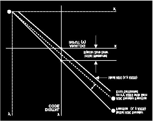
6 Figure 3a. Page 6 of 15

7 Figure 3b. Figures 3a and 3b. Calibrating bipolar offset error. (Note: The stair-step transfer function has been replaced by a straight line, because this graph shows all codes and the step size is so small that the line appears to be linear.) Unipolar systems are a little trickier. If the offset is positive, use the same methodology as that for bipolar supplies. The difference here is that you lose part of the ADC's range (see Figure 4). If the offset is negative, you cannot simply do a conversion and expect the result to represent the offset error. Below zero, the converter will just display zeros. Thus, with a negative offset error, you must increase the input voltage slowly to determine where the first ADC transition occurs. Here again you lose part of the ADC range. Page 7 of 15
].")
 = 2.492V. Any value above this will overrange the ADC.")
8 Figure 4. Unipolar offset error. Returning to our example, two scenarios for offset error are given below: 1. If the offset error is +8mV, with a 2.5V reference this corresponds to 13LSBs of error for a 12-bit ADC (8mV/[2.5V/4096)]. Though the resolution is still 12 bits, you must subtract 13 codes from each conversion result to compensate for the offset error. Note that the actual, measurable, fullscale value in this scenario is now 2.5V (4083/4096) = 2.492V. Any value above this will overrange the ADC. So, the dynamic range, or range of input values, for the ADC has been reduced. This is even more important for higher-resolution ADCs; 8mV represents 210LSBs at the 16-bit level (V REF = 2.5V). 2. If the offset is -8mV (assuming a unipolar input), then small analog-input values near zero will not register when a conversion is performed until the analog input exceeds +8mV. This too reduces the dynamic range of the ADC. Gain error is defined as the full-scale error minus the offset error (Figure 5). Full-scale error is measured at the last ADC transition on the transfer-function curve and compared against the ideal ADC transfer function. Gain error is easily corrected in software with a linear function y = (m1/m2)(x), where m1 is the slope of the ideal transfer function and m2 is the slope of the measured transfer function (Figure 5). Page 8 of 15

9 Figure 5. Offset, gain, and full-scale errors. The gain-error specification may or may not include errors contributed by the ADC's voltage reference. In the electrical specifications, it is important to check the conditions to see how gain error is tested and to determine whether it is performed with an internal or external reference. Typically, the gain error is much worse when an on-chip reference is used. If the gain error were zero, when a conversion is performed the conversion result would begin to yield all ones (3FFh in our 12-bit example) when the full-scale analog input is applied (see Figure 6). As our converter is not ideal, you can initially end up with all ones in the conversion result when a voltage greater than full-scale is applied (negative gain error) or when a voltage less than full-scale is applied (positive gain error). Two ways to adjust for gain error are to either tweak the reference voltage such that at a specific reference-voltage value the output gives fullscale or use a linear correction curve in software to change the slope of the ADC transfer-function curve (a first-order linear equation or a lookup table can be used). Page 9 of 15
, this is defined as negative gain error, and in this case the")

10 Figure 6. Gain error reduces dynamic range. As with offset error, you lose dynamic range with gain error. For example, if a full-scale input voltage is applied and the code obtained is 4050 instead of the ideal 4096 (for a 12-bit converter), this is defined as negative gain error, and in this case the upper 46 codes will not be used. Similarly, if the full-scale code of 4096 appears with an input voltage less than full-scale, the ADC's dynamic range is again reduced (see Figure 6). Note that, with positive full-scale errors, you cannot calibrate beyond the point where the converter gives all ones in the conversion result. The easiest way to handle offset and gain errors is to find an ADC with values low enough so that you don't have to calibrate. It's fairly easy to find 12-bit ADCs with offset and gain errors less than 4LSB. Other Subtle Error Sources Code-Edge Noise Code-edge noise is the amount of noise that appears right at a code transition on the transfer function. It is often not specified in the data sheet. Even higher-resolution converters (16+ bits), where code-edge noise is much more prevalent due to the smaller LSB size, will often not specify code-edge noise. Sometimes, code-edge noise can be several LSBs. Conversions performed with the analog input right at the code edge can result in code flicker in the LSBs. Significant code-edge noise means that an average of samples must be taken to effectively remove this noise from the converter results. How many samples are needed? If the code-edge noise is 2/3LSB RMS, this equates to approximately 4LSB p-p. Sixteen samples will have to be taken to reduce the noise to 1LSB (the square root of the number of samples determines the improvement in performance). The Reference One of the biggest potential sources of errors in an ADC with an internal or external reference is the Page 10 of 15

.")


11 reference voltage. Often, if the reference is included on-chip, it is not specified adequately. To understand the source of the reference errors, it is important to look at three specs in particular: temperature drift, voltage noise, and load regulation. Temperature Drift Temperature drift is the most overlooked specification in the data sheet. As an example, note how temperature drift affects the performance of an ADC converter based on resolution (Figure 7). For a 12- bit converter to maintain accuracy over the extended temperature range (-40 C to +85 C), the drift must be a maximum of 4ppm/ C. Unfortunately, no ADC converter is available with this kind of on-chipreference performance. If we relax the requirements, a 10-degree temperature excursion means the 12- bit ADC reference can drift no more than 25ppm/ C, which again is a fairly tight requirement for on-chip references. Prototyping frequently does not reveal the significance of this error, because parts are often from a similar lot and thus the test results do not take into account the extremes that occur in specs due to manufacturing-process variations. Figure 7. Voltage-reference-drift requirements relate to ADC resolution. For some systems, the reference accuracy is not a big issue, as the temperature is held constant, eliminating the drift problem. Some systems use a ratiometric measurement, where the reference errors are removed because the same signal that excites the sensor is used as the reference voltage (Figure 8). Because the excitation source and reference move as one, drift errors are eliminated. Figure 8. Ratiometric ADC conversion. In other systems, calibration is performed often enough so that reference drift is effectively removed. In still other systems, absolute accuracy is not critical, but relative accuracy is. Therefore, the reference can Page 11 of 15
12 drift slowly with time and the system will provide the desired accuracy. Voltage Noise Another important spec is voltage noise. It is often specified as either an RMS value or a peak-to-peak value. Convert the RMS value to a peak-to-peak value to evaluate its effect on performance. If a 2.5V reference has 500µV of peak-to-peak voltage noise at the output (or 83µV RMS), this noise represents 0.02% error or barely 12-bit performance, and this is before any of the converter errors are considered. Ideally, our reference-noise performance should be a small fraction of an LSB so as not to limit the ADC's performance. ADCs with on-chip references usually don't specify voltage noise, so the error is up to the user to determine. If you are not getting the performance you desire and are using an internal reference, try using a very good external reference to determine if the on-chip reference is in fact the culprit. Load Regulation The final spec is reference load regulation. Often the voltage reference used for an ADC has ample current to drive other devices, so it is used by other ICs. The current drawn by those other components will affect the voltage reference, which means that as more current is drawn the reference voltage will droop. If the devices using the reference are turning on and off intermittently, the result will be a reference voltage that moves up and down. A 0.55µV/µA reference-load-regulation specification for a 2.5V reference means that, if other devices draw 800µA, the reference voltage will change up to 440µV, which is.0176% (440µV/2.5V) or almost 20% of the available error margin. Other Temperature Effects Continuing with the topic of temperature, two specifications that are often given little attention are offset drift and gain drift. These specs are usually given as typical numbers only, leaving it up to the users to determine if the specification is good enough for their system requirements. Offset- and gain-drift values can be compensated in a couple of different ways. One way is to fully characterize the offset and gain drift, and provide a lookup table in memory to adjust the values as temperature changes. This, however, is a cumbersome process, as each ADC must be compensated individually and the compensation process is a time-consuming effort. The second method is to perform calibrations when a significant temperature change has occurred. With systems that do a one-time temperature calibration, it's important to pay heed to the drift specs. If the initial offset is calibrated and the temperature moves, there will be an error introduced due to the drift term that can negate the effects of the calibration. For example, assume a reading is done at temperature X. Some time later, the temperature has changed 10 C and the exact same measurement is taken. These two readings can give different results, calling into question the repeatability and thus the reliability of the system. There is a good reason why manufacturers do not give maximum limits: This increases the cost. Drift testing requires special boards, and an extra step must be added to the test flow (which equates to an additional manufacturing cost) to make sure the parts do not exceed the maximum-drift limit. Gain drift is more of an issue, particularly for devices tested with an internal reference. In this case, the reference drift can be included in the gain-drift parameter. For an external reference, the IC's gain drift is typically fairly small, like 0.8ppm/ C. Thus, a +/-10 degree temperature change results in a +/-8ppm change. Note that 12-bit performance equates to 244ppm (1/4096 = % = 244ppm). So, we see an error that represents only a fraction of an LSB at the 12-bit level. AC Performance Page 12 of 15

13 Some ADCs perform well only with input signals at or near DC. Others perform well with input signals from DC up to Nyquist. Just because DNL and INL meet the system requirements does not mean the converter will give that same performance when AC signals are considered. DNL and INL are DC tests. We must look to the AC specs to get a good feeling for AC performance. The Electrical Characteristics table and the Typical Operating Characteristics found in the data sheet offer clues to the AC performance. The key specs to review are signal-to-noise ratio (SNR), signal-to-noise and distortion ratio (SINAD), total harmonic distortion (THD), and spurious-free dynamic range (SFDR). The first specification to review is SINAD or SNR. SINAD is defined as the RMS value of an input sine wave to the RMS value of the noise of the converter (from DC to the Nyquist frequency, including harmonic [total harmonic distortion] content). Harmonics occur at multiples of the input frequency (see Figure 9). SNR is similar to SINAD, except that it does not include the harmonic content. Thus, the SNR should always be better than the SINAD. Both SINAD and SNR are typically expressed in db. where N is the number of bits. For an ideal 12-bit converter, the SINAD is 74dB. Should this equation be rewritten in terms of N, it would reveal how many bits of information are obtained as a function of the RMS noise: This equation is the definition for effective number of bits, or ENOB. Figure 9. FFT plot reveals AC performance of an ADC. Note that SINAD is a function of the input frequency. As frequency increases toward the Nyquist limit, SINAD decreases. If the specification in the data sheet is tested at low frequencies compared to the Nyquist frequency, you can bet the performance will be much worse near Nyquist. Look for an ENOB graph in the Typical Operating Characteristics of the data sheet. ENOB degrades with frequency primarily because THD gets increasingly worse as the input frequency increases. For example, with a SINAD minimum value of 68dB at the frequency of interest, you obtain an ENOB value of 11. Therefore, you have lost 1 bit of information due to the converter's noise and distortion performance. This means that your 12-bit converter can provide only 0.05% accuracy at best. Remember that INL is a DC spec; ENOB is the specification that tells about nonlinearities for AC signals. Page 13 of 15
14 SNR is the signal-to-noise ratio with the distortion components removed. SNR reveals where the noise floor of the converter is. There can be a steep decrease in SNR as a function of input frequency, which means the converter was not designed for frequencies near this point. One way to improve SNR is to oversample, which provides a processing gain. Oversampling is a method of lowering the noise floor of the converter by sampling at a rate much higher than the signal of interest. This spreads the noise out over a wider range in the frequency domain, thereby effectively reducing the noise at any one frequency bin. A 2X oversampling reduces the noise floor by 3dB. SFDR is defined as the ratio of the RMS value of an input sine wave to the RMS value of the largest spur observed in the frequency domain using an FFT plot. It is typically expressed in db. SFDR is important in certain communication applications that require maximizing the dynamic range of the ADC. Spurs prevent the ADC from converting small input signals, because the distortion component can be much larger than the signal of interest. This limits the dynamic range of the ADC. Note that a large spur in the frequency domain may not significantly affect the SNR, but will significantly affect the SFDR. Final Thoughts Returning to the ADC example, assume we are measuring DC-type signals and our ADC accepts bipolar input signals. We choose the B grade of the MAX1241, which has 1LSB DNL error, 1LSB INL error (0.0244%), 3LSB offset error (3/4096 = %), and gain of 4LSB (0.0977%). Adding the errors, we obtain a total error of %. We can calibrate out the offset and gain errors, dropping our error to %. As long as our voltage-reference error is less than 0.075% % = 0.051%, we are within the error budget. A 5ppm/ C drift of more than 50 degrees equates to a 0.025% drift error, with a 0.026% error budget remaining. For 12-bit performance, we need to have a voltage reference with a voltage-noise specification considerably less than 1LSB (which is 2.5V/4096 = 610µV peak-to-peak or 102µV RMS). The MAX6166 is a good choice with 5ppm/ C drift and 30µV RMS wideband voltage noise. It also has ample source and sink current capability to drive the ADC (and additional circuitry if needed). Note that the 30µV noise spec equates to 180µV peak-to-peak, which is one-third of an LSB at the 12- bit level and one-sixth of an LSB at the 11-bit level (which is what our system requirement actually is). A quick check of the MAX1241 gain drift reveals a specification of 0.25ppm/ C or 12.5ppm over a 50 C temperature change, which is well within spec. Now we have a viable solution that should prevent any hidden performance hiccups due to the specifications. Note for this example that we didn't address the AC performance at all. However, with your better understanding of the ADC specs and how they relate to the converter's performance, you will be armed with enough information to select the ADC that will give you the performance you need. Related Parts MAX1280 MAX1281 MAX1290 MAX ksps/300ksps, Single-Supply, Low-Power, 8-Channel, Serial 12-Bit ADCs with Internal Reference 400ksps/300ksps, Single-Supply, Low-Power, 8-Channel, Serial 12-Bit ADCs with Internal Reference 400ksps, +5V, 8-/4-Channel, 12-Bit ADCs with +2.5V Reference and Parallel Interface 250ksps, +3V, 8-/4-Channel, 12-Bit ADCs with +2.5V Reference and Parallel Interface Free Samples Free Samples Free Samples Free Samples Page 14 of 15
15 More Information For Technical Support: For Samples: Other Questions and Comments: Application Note 748: TUTORIAL 748, AN748, AN 748, APP748, Appnote748, Appnote 748 Copyright by Maxim Integrated Products Additional Legal Notices: Page 15 of 15
MSP430 Teaching Materials
 MSP430 Teaching Materials Chapter 9 Data Acquisition A/D Conversion Introduction Texas Instruments t Incorporated University of Beira Interior (PT) Pedro Dinis Gaspar, António Espírito Santo, Bruno Ribeiro,
The Importance of Data Converter Static Specifications Don't Lose Sight of the Basics! by Walt Kester
 TUTORIAL The Importance of Data Converter Static Specifications Don't Lose Sight of the Basics! INTRODUCTION by Walt Kester In the 1950s and 1960s, dc performance specifications such as integral nonlinearity,
TUTORIAL 283 INL/DNL Measurements for High-Speed Analog-to- Digital Converters (ADCs)
") Maxim > Design Support > Technical Documents > Tutorials > A/D and D/A Conversion/Sampling Circuits > APP 283 Maxim > Design Support > Technical Documents > Tutorials > High-Speed Signal Processing > APP
Maxim > Design Support > Technical Documents > Tutorials > A/D and D/A Conversion/Sampling Circuits > APP 283 Maxim > Design Support > Technical Documents > Tutorials > High-Speed Signal Processing > APP
APPLICATION NOTE 3942 Optimize the Buffer Amplifier/ADC Connection
 Maxim > Design Support > Technical Documents > Application Notes > Communications Circuits > APP 3942 Maxim > Design Support > Technical Documents > Application Notes > High-Speed Interconnect > APP 3942
APPLICATION NOTE. Atmel AVR127: Understanding ADC Parameters. Atmel 8-bit Microcontroller. Features. Introduction
 APPLICATION NOTE Atmel AVR127: Understanding ADC Parameters Atmel 8-bit Microcontroller Features Getting introduced to ADC concepts Understanding various ADC parameters Understanding the effect of ADC
Fundamentals of Data Converters. DAVID KRESS Director of Technical Marketing
 Fundamentals of Data Converters DAVID KRESS Director of Technical Marketing 9/14/2016 Analog to Electronic Signal Processing Sensor (INPUT) Amp Converter Digital Processor Actuator (OUTPUT) Amp Converter
Data Converters. Specifications for Data Converters. Overview. Testing and characterization. Conditions of operation
 Data Converters Overview Specifications for Data Converters Pietro Andreani Dept. of Electrical and Information Technology Lund University, Sweden Conditions of operation Type of converter Converter specifications
APPLICATION NOTE 5581 CHALLENGE THE CONVENTIONAL - MAKE UNIPOLAR DACS BIPOLAR
 Keywords: unipolar, DAC, bipolar, analog IC, op amp, voltage reference, Kirchhoff current law, resistor matching, tolerance, temperature coefficient, offset, gain error, INL, DNL, calibrate, feedback,
ADC Resolution: Myth and Reality
 ADC Resolution: Myth and Reality Mitch Ferguson, Applications Engineering Manager Class ID: CC19I Renesas Electronics America Inc. Mr. Mitch Ferguson Applications Engineering Manager Specializes support
Different Digital Method
 Maxim > App Notes > DIGITAL POTENTIOMETERS Keywords: Digital Adjustment of DC-DC Converter Output Voltage in Portable Applications Oct 02, 2001 APPLICATION NOTE 818 Digital Adjustment of DC-DC Converter
Four-Channel Sample-and-Hold Amplifier AD684
 a FEATURES Four Matched Sample-and-Hold Amplifiers Independent Inputs, Outputs and Control Pins 500 ns Hold Mode Settling 1 s Maximum Acquisition Time to 0.01% Low Droop Rate: 0.01 V/ s Internal Hold Capacitors
The need for Data Converters
 The need for Data Converters ANALOG SIGNAL (Speech, Images, Sensors, Radar, etc.) PRE-PROCESSING (Filtering and analog to digital conversion) DIGITAL PROCESSOR (Microprocessor) POST-PROCESSING (Digital
Testing A/D Converters A Practical Approach
 Testing A/D Converters A Practical Approach Mixed Signal The seminar entitled Testing Analog-to-Digital Converters A Practical Approach is a one-day information intensive course, designed to address the
Oversampled ADC and PGA Combine to Provide 127-dB Dynamic Range
 Oversampled ADC and PGA Combine to Provide 127-dB Dynamic Range By Colm Slattery and Mick McCarthy Introduction The need to measure signals with a wide dynamic range is quite common in the electronics
Single-channel power supply monitor with remote temperature sense, Part 1
 Single-channel power supply monitor with remote temperature sense, Part 1 Nathan Enger, Senior Applications Engineer, Linear Technology Corporation - June 03, 2016 Introduction Many applications with a
AD Bit, 20/40/65 MSPS 3 V Low Power A/D Converter. Preliminary Technical Data
 FEATURES Ultra Low Power 90mW @ 0MSPS; 135mW @ 40MSPS; 190mW @ 65MSPS SNR = 66.5 dbc (to Nyquist); SFDR = 8 dbc @.4MHz Analog Input ENOB = 10.5 bits DNL=± 0.5 LSB Differential Input with 500MHz Full Power
4-Channel, 16-Bit, 200 ksps Data Acquisition System AD974
 a FEATURES Fast 16-Bit ADC with 200 ksps Throughput Four Single-Ended Analog Input Channels Single 5 V Supply Operation Input Ranges: 0 V to 4 V, 0 V to 5 V and 10 V 120 mw Max Power Dissipation Power-Down
A 12 bit 125 MHz ADC USING DIRECT INTERPOLATION
 A 12 bit 125 MHz ADC USING DIRECT INTERPOLATION Dr R Allan Belcher University of Wales Swansea and Signal Conversion Ltd, 8 Bishops Grove, Swansea SA2 8BE Phone +44 973 553435 Fax +44 870 164 0107 E-Mail:
APPLICATION NOTE 6206 SIMPLE, EFFECTIVE METHOD AND CIRCUIT TO MEASURE VERY-LOW 1/F VOLTAGE REFERENCE NOISE (< 1ΜV P-P, 0.
 Keywords: 0.1 to 10 Hz noise of voltage reference, low frequency noise or flicker noise of voltage reference, ultra low noise measurement of voltage reference APPLICATION NOTE 606 SIMPLE, EFFECTIVE METHOD
APPLICATION NOTE 695 New ICs Revolutionize The Sensor Interface
 Maxim > Design Support > Technical Documents > Application Notes > Sensors > APP 695 Keywords: high performance, low cost, signal conditioner, signal conditioning, precision sensor, signal conditioner,
16-Bit, 135ksps, Single-Supply ADCs with Bipolar Analog Input Range
 19-2755; Rev 1; 8/3 16-Bit, 135ksps, Single-Supply ADCs with General Description The 16-bit, low-power, successiveapproximation analog-to-digital converters (ADCs) feature automatic power-down, a factory-trimmed
Overall Accuracy = ENOB (Effective Number of Bits)
") Overall Accuracy = ENOB (Effective Number of Bits) In choosing a data acquisition board, there is probably no more important specification than its overall accuracy that is, how closely the output data
Overall Accuracy = ENOB (Effective Number of Bits) In choosing a data acquisition board, there is probably no more important specification than its overall accuracy that is, how closely the output data
Analyzing A/D and D/A converters
 Analyzing A/D and D/A converters 2013. 10. 21. Pálfi Vilmos 1 Contents 1 Signals 3 1.1 Periodic signals 3 1.2 Sampling 4 1.2.1 Discrete Fourier transform... 4 1.2.2 Spectrum of sampled signals... 5 1.2.3
16-Bit, 135ksps, Single-Supply ADCs with Bipolar Analog Input Range
 19-2675; Rev 1; 1/3 16-Bit, 135ksps, Single-Supply ADCs with General Description The 16-bit, low-power, successive-approximation analog-to-digital converters (ADCs) feature automatic power-down, a factorytrimmed
781/ /
 781/329-47 781/461-3113 SPECIFICATIONS DC SPECIFICATIONS J Parameter Min Typ Max Units SAMPLING CHARACTERISTICS Acquisition Time 5 V Step to.1% 25 375 ns 5 V Step to.1% 2 35 ns Small Signal Bandwidth 15
ADCS7476/ADCS7477/ADCS7478 1MSPS, 12-/10-/8-Bit A/D Converters in 6-Lead SOT-23
 ADCS7476/ADCS7477/ADCS7478 1MSPS, 12-/10-/8-Bit A/D Converters in 6-Lead SOT-23 General Description The ADCS7476, ADCS7477, and ADCS7478 are low power, monolithic CMOS 12-, 10- and 8-bit analog-to-digital
FUNCTIONAL BLOCK DIAGRAM DIGITAL VIDEO ENGINE
 FEATURES CMOS DUAL CHANNEL 10bit 40MHz DAC LOW POWER DISSIPATION: 180mW(+3V) DIFFERENTIAL NONLINEARITY ERROR: 0.5LSB SIGNAL-to-NOISE RATIO: 59dB SPURIOUS-FREE DYNAMIC RANGE:69dB BUILD-IN DIGITAL ENGINE
Serial Input 18-Bit Monolithic Audio DIGITAL-TO-ANALOG CONVERTER
 Serial Input 8-Bit Monolithic Audio DIGITAL-TO-ANALOG CONVERTER FEATURES 8-BIT MONOLITHIC AUDIO D/A CONVERTER LOW MAX THD + N: 92dB Without External Adjust 00% PIN COMPATIBLE WITH INDUSTRY STD 6-BIT PCM56P
1MHz PWM STEP-DOWN CONVERTER
 .5G G ABC 6 kv 7 V 9 FM MHz PWM STEP-DOWN CONVERTER Li+ BATTERY.7V TO 4.V V OUT CONTROL DAC SYNC REF BATT MAX80 LX OUT 4.7µH V OUT 4.7µF MHz OR 9.8MHz SYSTEM CLOCK BASEBAND PROCESSOR GND RF TRANSMIT SECTION
Serial Input 18-Bit Monolithic Audio DIGITAL-TO-ANALOG CONVERTER
 Serial Input 8-Bit Monolithic Audio DIGITAL-TO-ANALOG CONVERTER FEATURES 8-BIT MONOLITHIC AUDIO D/A CONVERTER LOW MAX THD + N: 92dB Without External Adjust 00% PIN COMPATIBLE WITH INDUSTRY STD 6-BIT PCM56P
Enhancing Analog Signal Generation by Digital Channel Using Pulse-Width Modulation
 Enhancing Analog Signal Generation by Digital Channel Using Pulse-Width Modulation Angelo Zucchetti Advantest angelo.zucchetti@advantest.com Introduction Presented in this article is a technique for generating
Lecture 9, ANIK. Data converters 1
 Lecture 9, ANIK Data converters 1 What did we do last time? Noise and distortion Understanding the simplest circuit noise Understanding some of the sources of distortion 502 of 530 What will we do today?
Input Stage Concerns. APPLICATION NOTE 656 Design Trade-Offs for Single-Supply Op Amps
 Maxim/Dallas > App Notes > AMPLIFIER AND COMPARATOR CIRCUITS Keywords: single-supply, op amps, amplifiers, design, trade-offs, operational amplifiers Apr 03, 2000 APPLICATION NOTE 656 Design Trade-Offs
Data Converter Fundamentals
 IsLab Analog Integrated Circuit Design Basic-25 Data Converter Fundamentals כ Kyungpook National University IsLab Analog Integrated Circuit Design Basic-1 A/D Converters in Signal Processing Signal Sources
Application Note 80. July How to Use the World s Smallest 24-Bit No Latency Delta-Sigma TM ADC to its Fullest Potential AN80-1
 July 1999 How to Use the World s Smallest 24-Bit No Latency Delta-Sigma TM ADC to its Fullest Potential Frequently Asked Questions About Delta-Sigma ADCs and the LTC2400 By Michael K. Mayes Linear Technology
DATASHEET HI5805. Features. Applications. Ordering Information. Pinout. 12-Bit, 5MSPS A/D Converter. FN3984 Rev 7.00 Page 1 of 12.
 12-Bit, 5MSPS A/D Converter NOT RECOMMENDED FOR NEW DESIGNS NO RECOMMENDED REPLACEMENT contact our Technical Support Center at 1-888-INTERSIL or www.intersil.com/tsc DATASHEET FN3984 Rev 7.00 The HI5805
PRODUCT OVERVIEW REF FLASH ADC S/H BUFFER 24 +5V SUPPLY +12V/+15V SUPPLY. Figure 1. ADS-917 Functional Block Diagram
 PRODUCT OVERVIEW The is a high-performance, 14-bit, 1MHz sampling A/D converter. This device samples input signals up to Nyquist frequencies with no missing codes. The features outstanding dynamic performance
National Instruments Flex II ADC Technology The Flexible Resolution Technology inside the NI PXI-5922 Digitizer
 National Instruments Flex II ADC Technology The Flexible Resolution Technology inside the NI PXI-5922 Digitizer Kaustubh Wagle and Niels Knudsen National Instruments, Austin, TX Abstract Single-bit delta-sigma
SECTION 4 HIGH SPEED SAMPLING AND HIGH SPEED ADCs, Walt Kester
 SECTION 4 HIGH SPEED SAMPLING AND HIGH SPEED ADCs, Walt Kester INTRODUCTION High speed ADCs are used in a wide variety of real-time DSP signal-processing applications, replacing systems that used analog
Lecture #6: Analog-to-Digital Converter
 Lecture #6: Analog-to-Digital Converter All electrical signals in the real world are analog, and their waveforms are continuous in time. Since most signal processing is done digitally in discrete time,
Acquisition Time: Refer to Figure 1 when comparing SAR, Pipeline, and Delta-Sigma converter acquisition time. Signal Noise. Data Out Pipeline ADC
 Application Report SBAA147A August 2006 Revised January 2008 A Glossary of Analog-to-Digital Specifications and Performance Characteristics Bonnie Baker... Data Acquisition Products ABSTRACT This glossary
Section 1. Fundamentals of DDS Technology
 Section 1. Fundamentals of DDS Technology Overview Direct digital synthesis (DDS) is a technique for using digital data processing blocks as a means to generate a frequency- and phase-tunable output signal
DAC & ADC Testing Fundamental
 DAC & ADC Testing Fundamental Outline Specifications of DAC Specifications of ADC Test methodology Static specification Histogram method Transfer (and compare) method Dynamic specification FFT Polynomial
4-Channel, 1 MSPS, 8-/10-/12-Bit ADCs with Sequencer in 16-Lead TSSOP AD7904/AD7914/AD7924
 a 4-Channel, 1 MSPS, 8-/10-/12-Bit ADCs with Sequencer in 16-Lead TSSOP AD7904/AD7914/AD7924 FEATURES Fast Throughput Rate: 1 MSPS Specified for V DD of 2.7 V to 5.25 V Low Power: 6 mw max at 1 MSPS with
Design of Pipeline Analog to Digital Converter
 Design of Pipeline Analog to Digital Converter Vivek Tripathi, Chandrajit Debnath, Rakesh Malik STMicroelectronics The pipeline analog-to-digital converter (ADC) architecture is the most popular topology
Hideo Okawara s Mixed Signal Lecture Series. DSP-Based Testing Fundamentals 6 Spectrum Analysis -- FFT
 Hideo Okawara s Mixed Signal Lecture Series DSP-Based Testing Fundamentals 6 Spectrum Analysis -- FFT Verigy Japan October 008 Preface to the Series ADC and DAC are the most typical mixed signal devices.
5 V, 14-Bit Serial, 5 s ADC in SO-8 Package AD7894
 a FEATURES Fast 14-Bit ADC with 5 s Conversion Time 8-Lead SOIC Package Single 5 V Supply Operation High Speed, Easy-to-Use, Serial Interface On-Chip Track/Hold Amplifier Selection of Input Ranges 10 V
System on a Chip. Prof. Dr. Michael Kraft
 System on a Chip Prof. Dr. Michael Kraft Lecture 5: Data Conversion ADC Background/Theory Examples Background Physical systems are typically analogue To apply digital signal processing, the analogue signal
Working with ADCs, OAs and the MSP430
 Working with ADCs, OAs and the MSP430 Bonnie Baker HPA Senior Applications Engineer Texas Instruments 2006 Texas Instruments Inc, Slide 1 Agenda An Overview of the MSP430 Data Acquisition System SAR Converters
Data Conversion Techniques (DAT115)
") Data Conversion Techniques (DAT115) Hand in Report Second Order Sigma Delta Modulator with Interleaving Scheme Group 14N Remzi Yagiz Mungan, Christoffer Holmström [ 1 20 ] Contents 1. Task Description...
Data Conversion Techniques (DAT115) Hand in Report Second Order Sigma Delta Modulator with Interleaving Scheme Group 14N Remzi Yagiz Mungan, Christoffer Holmström [ 1 20 ] Contents 1. Task Description...
16-Channel, 1 MSPS, 12-Bit ADC with Sequencer in 28-Lead TSSOP AD7490
 a FEATURES Fast Throughput Rate: 1 MSPS Specified for V DD of 2.7 V to 5.25 V Low Power at Max Throughput Rates: 5.4 mw Max at 870 ksps with 3 V Supplies 12.5 mw Max at 1 MSPS with 5 V Supplies 16 (Single-Ended)
5 V, 12-Bit, Serial 3.8 s ADC in 8-Pin Package AD7895
 a FEATURES Fast 12-Bit ADC with 3.8 s Conversion Time 8-Pin Mini-DlP and SOIC Single 5 V Supply Operation High Speed, Easy-to-Use, Serial Interface On-Chip Track/Hold Amplifier Selection of Input Ranges
400ksps/300ksps, Single-Supply, Low-Power, Serial 12-Bit ADCs with Internal Reference
 19-1687; Rev 2; 12/10 EVALUATION KIT AVAILABLE General Description The 12-bit analog-to-digital converters (ADCs) combine a high-bandwidth track/hold (T/H), a serial interface with high conversion speed,
8-/4-/2-Channel, 14-Bit, Simultaneous-Sampling ADCs with ±10V, ±5V, and 0 to +5V Analog Input Ranges
 19-3157; Rev 4; 10/08 8-/4-/2-Channel, 14-Bit, Simultaneous-Sampling ADCs General Description The MAX1316 MAX1318/MAX1320 MAX1322/MAX1324 MAX1326 14-bit, analog-to-digital converters (ADCs) offer two,
SPT BIT, 30 MSPS, TTL, A/D CONVERTER
 12-BIT, MSPS, TTL, A/D CONVERTER FEATURES Monolithic 12-Bit MSPS Converter 6 db SNR @ 3.58 MHz Input On-Chip Track/Hold Bipolar ±2.0 V Analog Input Low Power (1.1 W Typical) 5 pf Input Capacitance TTL
High Speed System Applications
 High Speed System Applications 1. High Speed Data Conversion Overview 2. Optimizing Data Converter Interfaces 3. DACs, DDSs, PLLs, and Clock Distribution 4. PC Board Layout and Design Tools Copyright 2006
Oscilloscope Measurement Fundamentals: Vertical-Axis Measurements (Part 1 of 3)
") Oscilloscope Measurement Fundamentals: Vertical-Axis Measurements (Part 1 of 3) This article is the first installment of a three part series in which we will examine oscilloscope measurements such as the
Oscilloscope Measurement Fundamentals: Vertical-Axis Measurements (Part 1 of 3) This article is the first installment of a three part series in which we will examine oscilloscope measurements such as the
Complete 12-Bit 1.25 MSPS Monolithic A/D Converter AD1671
 a FEATURES Conversion Time: 800 ns 1.25 MHz Throughput Rate Complete: On-Chip Sample-and-Hold Amplifier and Voltage Reference Low Power Dissipation: 570 mw No Missing Codes Guaranteed Signal-to-Noise Plus
The Fundamentals of Mixed Signal Testing
 The Fundamentals of Mixed Signal Testing Course Information The Fundamentals of Mixed Signal Testing course is designed to provide the foundation of knowledge that is required for testing modern mixed
5 V, 12-Bit, Serial 220 ksps ADC in an 8-Lead Package AD7898 * REV. A
 a FEATURES Fast 12-Bit ADC with 220 ksps Throughput Rate 8-Lead SOIC Single 5 V Supply Operation High Speed, Flexible, Serial Interface that Allows Interfacing to 3 V Processors On-Chip Track/Hold Amplifier
INTEGRATED CIRCUITS. AN109 Microprocessor-compatible DACs Dec
 INTEGRATED CIRCUITS 1988 Dec DAC products are designed to convert a digital code to an analog signal. Since a common source of digital signals is the data bus of a microprocessor, DAC circuits that are
FUNDAMENTALS OF OSCILLOSCOPE MEASUREMENTS IN AUTOMATED TEST EQUIPMENT (ATE)
") FUNDAMENTALS OF OSCILLOSCOPE MEASUREMENTS IN AUTOMATED TEST EQUIPMENT (ATE) Creston D. Kuenzi ZTEC Instruments 7715 Tiburon St. NE Albuquerque, NM 87109 505-342-0132 ckuenzi@ztec-inc.com Christopher D.
FUNDAMENTALS OF OSCILLOSCOPE MEASUREMENTS IN AUTOMATED TEST EQUIPMENT (ATE) Creston D. Kuenzi ZTEC Instruments 7715 Tiburon St. NE Albuquerque, NM 87109 505-342-0132 ckuenzi@ztec-inc.com Christopher D.
LC 2 MOS 8-Channel, 12-Bit Serial, Data Acquisition System AD7890
 a LC 2 MOS 8-Channel, 12-Bit Serial, Data Acquisition System AD7890 FEATURES Fast 12-Bit ADC with 5.9 s Conversion Time Eight Single-Ended Analog Input Channels Selection of Input Ranges: 10 V for AD7890-10
DYNAMIC BEHAVIOR MODELS OF ANALOG TO DIGITAL CONVERTERS AIMED FOR POST-CORRECTION IN WIDEBAND APPLICATIONS
 XVIII IMEKO WORLD CONGRESS th 11 WORKSHOP ON ADC MODELLING AND TESTING September, 17 22, 26, Rio de Janeiro, Brazil DYNAMIC BEHAVIOR MODELS OF ANALOG TO DIGITAL CONVERTERS AIMED FOR POST-CORRECTION IN
TLV1572ID 2.7 V TO 5.5 V, 10-BIT, 1.25 MSPS SERIAL ANALOG-TO-DIGITAL CONVERTER WITH AUTO-POWERDOWN. Applications. description
 Fast Throughput Rate: 1.25 MSPS 8-Pin SOIC Package Differential Nonlinearity Error: < ± 1 LSB Integral Nonlinearity Error: < ± 1 LSB Signal-to-Noise and Distortion Ratio: 59 db, f (input) = 500 khz Single
Analog and Telecommunication Electronics
 Politecnico di Torino Electronic Eng. Master Degree Analog and Telecommunication Electronics D6 - High speed A/D converters» Spectral performance analysis» Undersampling techniques» Sampling jitter» Interleaving
Direct Digital Down/Up Conversion for RF Control of Accelerating Cavities
 Direct Digital Down/Up Conversion for RF Control of Accelerating Cavities C. Hovater, T. Allison, R. Bachimanchi, J. Musson and T. Plawski Introduction As digital receiver technology has matured, direct
New Features of IEEE Std Digitizing Waveform Recorders
 New Features of IEEE Std 1057-2007 Digitizing Waveform Recorders William B. Boyer 1, Thomas E. Linnenbrink 2, Jerome Blair 3, 1 Chair, Subcommittee on Digital Waveform Recorders Sandia National Laboratories
Analog to Digital Conversion
 Analog to Digital Conversion Florian Erdinger Lehrstuhl für Schaltungstechnik und Simulation Technische Informatik der Uni Heidelberg VLSI Design - Mixed Mode Simulation F. Erdinger, ZITI, Uni Heidelberg
Advantages of Analog Representation. Varies continuously, like the property being measured. Represents continuous values. See Figure 12.
 Analog Signals Signals that vary continuously throughout a defined range. Representative of many physical quantities, such as temperature and velocity. Usually a voltage or current level. Digital Signals
Features. Key Specifications. n Total unadjusted error. n No missing codes over temperature. Applications
 ADC10061/ADC10062/ADC10064 10-Bit 600 ns A/D Converter with Input Multiplexer and Sample/Hold General Description Using an innovative, patented multistep* conversion technique, the 10-bit ADC10061, ADC10062,
2.7 V to 5.5 V, 400 ksps 8-/10-Bit Sampling ADC AD7813
 a FEATURES 8-/10-Bit ADC with 2.3 s Conversion Time On-Chip Track and Hold Operating Supply Range: 2.7 V to 5.5 V Specifications at 2.7 V 3.6 V and 5 V 10% 8-Bit Parallel Interface 8-Bit + 2-Bit Read Power
Analog-to-Digital i Converters
 CSE 577 Spring 2011 Analog-to-Digital i Converters Jaehyun Lim, Kyusun Choi Department t of Computer Science and Engineering i The Pennsylvania State University ADC Glossary DNL (differential nonlinearity)
CMOS 12-Bit Serial Input Multiplying DIGITAL-TO-ANALOG CONVERTER
 CMOS 12-Bit Serial Input Multiplying DIGITAL-TO-ANALOG CONVERTER FEATURES 12-BICCURACY IN 8-PIN MINI-DIP AND 8-PIN SOIC FAST 3-WIRE SERIAL INTERFACE LOW INL AND DNL: ±1/2 LSB max GAIN ACCURACY TO ±1LSB
A-D and D-A Converters
 Chapter 5 A-D and D-A Converters (No mathematical derivations) 04 Hours 08 Marks When digital devices are to be interfaced with analog devices (or vice a versa), Digital to Analog converter and Analog
AD9772A - Functional Block Diagram
 F FEATURES single 3.0 V to 3.6 V supply 14-Bit DAC Resolution 160 MPS Input Data Rate 67.5 MHz Reconstruction Passband @ 160 MPS 74 dbc FDR @ 25 MHz 2 Interpolation Filter with High- or Low-Pass Response
Analog to Digital Converters
 Analog to Digital Converters ADC review ADC Types Pipelined Data Converter Design Basic concepts eview existing approaches Pipelined Design Strategies 1 Analog to Digital Converters Most widely used mixed-signal
DATASHEET HI1175. Features. Ordering Information. Applications. Pinout. 8-Bit, 20MSPS, Flash A/D Converter. FN3577 Rev 8.
 8-Bit, 2MSPS, Flash A/D Converter Pb-Free and RoHS Compliant DATASHEET FN377 Rev 8. The HI117 is an 8-bit, analog-to-digital converter built in a 1.4 m CMOS process. The low power, low differential gain
Eliminate Pipeline Headaches with New 12-Bit 3Msps SAR ADC by Dave Thomas and William C. Rempfer
 A new 12-bit 3Msps ADC brings new levels of performance and ease of use to high speed ADC applications. By raising the speed of the successive approximation (SAR) method to 3Msps, it eliminates the many
1 MSPS, Serial 14-Bit SAR ADC AD7485
 a FEATURES Fast Throughput Rate: 1 MSPS Wide Input Bandwidth: 4 MHz Excellent DC Accuracy Performance Flexible Serial Interface Low Power: 8 mw (Full Power) and 3 mw (NAP Mode) STANDBY Mode: A Max Single
FUNCTIONAL BLOCK DIAGRAM
 FEATURES 16-Bit - ADC 64 Oversampling Ratio Up to 220 ksps Output Word Rate Low-Pass, Linear Phase Digital Filter Inherently Monotonic On-Chip 2.5 V Voltage Reference Single-Supply 5 V High Speed Parallel
ADC Based Measurements: a Common Basis for the Uncertainty Estimation. Ciro Spataro
 ADC Based Measurements: a Common Basis for the Uncertainty Estimation Ciro Spataro Department of Electric, Electronic and Telecommunication Engineering - University of Palermo Viale delle Scienze, 90128
Maxim > Design Support > Technical Documents > Application Notes > Digital Potentiometers > APP 3408
 Maxim > Design Support > Technical Documents > Application Notes > Digital Potentiometers > APP 3408 Keywords: internal calibration, ADC, A/D, gain, offset, temperature compensated, digital resistor, analog
16-Bit DSP DACPORT AD766
 a FEATURES Zero-Chip Interface to Digital Signal Processors Complete DACPORT On-Chip Voltage Reference Voltage and Current Outputs Serial, Twos-Complement Input 3 V Output Sample Rates to 390 ksps 94 db
Dual, 12-Bit, 1.25Msps Simultaneous-Sampling ADCs with Serial Interface
 19-4126; Rev 1; 2/9 General Description The feature two simultaneous-sampling, low-power, 12-bit ADCs with serial interface and internal voltage reference. Fast sampling rate, low power dissipation, and
OBSOLETE. Monolithic 12-Bit 2 MHz A/D Converter AD671 REV. B FUNCTIONAL BLOCK DIAGRAM
 a FEATURES 12-Bit Resolution 2-Pin Skinny DIP Package Conversion Time: 500 ns max J/K/S-500 Conversion Time: 750 ns max J/K/S-750 Low Power: 75 mw Unipolar (0 V to +5 V, 0 V to +10 V) and Bipolar Input
Low Noise, Matched Dual PNP Transistor MAT03
 a FEATURES Dual Matched PNP Transistor Low Offset Voltage: 100 V Max Low Noise: 1 nv/ Hz @ 1 khz Max High Gain: 100 Min High Gain Bandwidth: 190 MHz Typ Tight Gain Matching: 3% Max Excellent Logarithmic
Dynamic Specifications for Sampling A D Converters
 Dynamic Specifications for Sampling A D Converters 1 0 INTRODUCTION Traditionally analog-to-digital converters (ADCs) have been specified by their static characteristics such as integral and differential
Analog-to-Digital Converter Survey & Analysis. Bob Walden. (310) Update: July 16,1999
 Update: July 16,1999") Analog-to-Digital Converter Survey & Analysis Update: July 16,1999 References: 1. R.H. Walden, Analog-to-digital converter survey and analysis, IEEE Journal on Selected Areas in Communications, vol. 17,
Analog-to-Digital Converter Survey & Analysis Update: July 16,1999 References: 1. R.H. Walden, Analog-to-digital converter survey and analysis, IEEE Journal on Selected Areas in Communications, vol. 17,
18-Bit, 500ksps, ±5V SAR ADC with Internal Reference in TDFN
 EVALUATION KIT AVAILABLE MAX11156 with Internal Reference in TDFN General Description The MAX11156 18-bit, 5ksps, SAR ADC offers excellent AC and DC performance with true bipolar input range, small size,
Linear Technology Chronicle
 Linear Technology Chronicle High Performance Analog Solutions from Linear Technology Vol. 13 No. 5 Industrial Process Control LT1790-2.5 LTC2054 REMOTE THERMOCOUPLE CH0 CH1 CH7 CH8 CH15 COM REF 16-CHANNEL
CMOS Sigma-Delta Modulator AD7720
 a FEATURES 12.5 MHz Master Clock Frequency V to +2.5 V or 1.25 V Input Range Single Bit Output Stream 9 Dynamic Range Power Supplies: AVDD, DVDD: +5 V 5% On-Chip 2.5 V Voltage Reference 28-Lead TSSOP VIN(+)
7809ALP 16-Bit Latchup Protected Analog to Digital Converter
 789ALP 6-Bit Latchup Protected Analog to Digital Converter R/C CS POWER DOWN Successive Approimation Register and Control Logic Clock 2 k CDAC R IN k BUSY R2 IN R3 IN 5 k 2 k Comparator Serial Data Out
LC 2 MOS Signal Conditioning ADC with RTD Current Source AD7711A *
 a FEATURES Charge Balancing ADC 24 Bits No Missing Codes 0.0015% Nonlinearity 2-Channel Programmable Gain Front End Gains from 1 to 128 Differential Inputs Low-Pass Filter with Programmable Filter Cutoffs
16-Bit, 250ksps, +5V SAR ADC with Internal Reference in µmax
 EVALUATION KIT AVAILABLE MAX11161 General Description The MAX11161 is a 16-bit, 250ksps, SAR ADC offering excellent AC and DC performance with true unipolar input range, internal reference, and small size.
Low-Power, 14-Bit Analog-to-Digital Converters with Parallel Interface
 19-2466; Rev 1; 6/9 General Description The 14-bit, low-power successive approximation analog-to-digital converters (ADCs) feature automatic power-down, a factory-trimmed internal clock, and a high-speed,
ADC78H90 8-Channel, 500 ksps, 12-Bit A/D Converter
 8-Channel, 500 ksps, 12-Bit A/D Converter General Description The ADC78H90 is a low-power, eight-channel CMOS 12-bit analog-to-digital converter with a conversion throughput of 500 ksps. The converter
CDK bit, 25 MSPS 135mW A/D Converter
 CDK1304 10-bit, 25 MSPS 135mW A/D Converter FEATURES n 25 MSPS converter n 135mW power dissipation n On-chip track-and-hold n Single +5V power supply n TTL/CMOS outputs n 5pF input capacitance n Tri-state
LC 2 MOS Loop-Powered Signal Conditioning ADC AD7713
 LC 2 MOS Loop-Powered Signal Conditioning ADC AD7713 FEATURES Charge Balancing ADC 24 Bits No Missing Codes 0.0015% Nonlinearity 3-Channel Programmable Gain Front End Gains from 1 to 128 2 Differential
AVS / DVS and Margining Circuits for Vishay Power ICs SiC40X Series SMPS Regulators
 VISHAY SILICONIX www.vishay.com ICs by Ronald Vinsant ABSTRACT There are many applications that require that a voltage rail within a system be capable of being adjusted by a digital or analog control signal.