Design and Implementation of Sequential Counters Using Reversible Logic Gates with Mach-Zehnder Interferometer
|
|
|
- Ethelbert Nicholson
- 5 years ago
- Views:
Transcription
1 Design and Implementation of Sequential Counters Using Reversible Logic Gates with Mach-Zehnder Interferometer A.Rudramadevi M.Tech(ES & VLSI Design), Nalgonda Institute of Technology and Science. P.Lachi Reddy, M.Tech,(Ph.D) Professor, Nalgonda Institute of Technology and Science. Abstract: This work presents all optical reversible implementation of sequential counters using semiconductor optical amplifier (SOA) based Mach- Zehnder interferometer (MZI) switches. With the advancements in semiconductor technology, there has been an increased emphasis in low-power design techniques over the last few decades. Reversible computing has been proposed by several researchers as a possible alternative to address the energy dissipation problem. Several implementation alternatives for reversible logic circuits have also been explored in recent years, like adiabatic logic, nuclear magnetic resonance, optical computing, etc. Recently researchers have proposed implementations of various reversible logic circuits in the all-optical computing domain. Most of these works are based on semiconductor optical amplifier (SOA) based Mach-Zehnder interferometer (MZI), which provides desirable features like low power, fast switching and ease of fabrication. All the designs are implemented using minimum number of MZI switches and garbage outputs. This design ensures improved optical costs in reversible realization of all the counter circuits. The theoretical model is simulated to verify the functionality of the circuits. Design complexity of all the proposed memory elements has been analysed. Keywords: Reversible computing, Mach-Zehnder Interferometer (MZI), counter, optical cost, optical delay, garbage. I. INTRODUCTION: Like Boolean logic functions, reversible logic function [1-3] is a special type of logic function where there always exists a bijective mapping between inputs to outputs. For a given reversible function, it is always possible to extract original inputs from its outputs correctly, that means it ensures no loss of information while retrieving original data. The concept of reversible logic was first introduced by Landauer [1] and Bennet [4]. According to their claims, if a process or function is reversible, then there is no loss of information which causes heat generation from the system. They also experimentally established that a certain amount of energy (KTlogn 2 Joules) would be dissipated as heat in the traditional logic computation for every bit of information loss during the computing process. So, it is seen that if a logic circuit can be made reversible, then it ensures zero heat dissipation [2] and no loss of information characteristics. The problems with traditional logic circuit has been highlighted by Ralph Merkle from Xerox PARC, who experimented [6] on 1GHz computer processor packed with 1018 traditional logic gates in a volume of 1 cm3operating at a room temperature and found that a huge amount of power nearly 3MW releases from the surface area of that processor. Now a day s, the VLSI industry is facing serious challenges due to the heat generation problem in Integrated Circuits (IC) and this problem will become severe in next years according to Moore's Law [7] due to the increasing miniaturization and the exponential growth of number of transistors in integrated circuits. To address these issues, the reversible computing has evolved as an alternative as it promises zero power dissipation [2] in the several emerging technologies like ultra low power Page 191
2 CMOS design, optical computing [5], nanotechnology [6] and DNA computing [1]. Design of the reversible carry-look-ahead adder using control gate and its physical implementation have been first reported in [8] where the circuit is powered by their input signals only and does not need any additional power supplies. Recently, the researchers are aiming at the development of the optical digital computer system for processing binary data using optical computation. Photons are the source of optical technology. This photonic particle provides unmatched speed with information as it has the speed of light. The installation of optical components in the electronic computer system produces optical-electronic hybrid network. The researchers are trying to combine the optical interconnects with the electronic computing devices. The implementation of reversible logic circuits with optical technology can be performed using Semiconductor Optical Amplifier (SOA) based Mach- Zehnder Interferometer (MZI) switches which has significant advantages of the high speed, low power, fast switching time and ease of fabrication [11-10]. The optical computing concept in design and synthesis of reversible logic circuit has first been introduced in [12]. Generalized implementation of reversible gate like Toffoli, Fredkin, and CNOT using optical technology has been reported in [10], where Mach Zehnder interferometer (MZI) is used to implement all-optical reversible logic gates. Reversible implementation of NOR gate using SOA based MZI switches is realized in [11]. The optical implementation of functionally reversible Mach- Zehnder Interferometer based binary adder has been proposed in [12], where two new optical reversible gates ORG-I and ORG-II have been proposed in addition to existing Feynman gate to implement the architecture. The implementation of All-optical XOR gate using SOA-based MZI and micro resonators has been reported in [13] and [14], respectively. Apart from use of MZI to design reversible gates, TOAD (terahertz optical asymmetric de-multiplexer)-based and alloptical fiber-based implementation of Fredkin gate is presented in [15] and [16], respectively. The sequential circuit is one of the most important components of the computer system and the efficient of the memory element is a primary concern in this circuit. As the reversible circuit promises information lossless and no heat generation property, an intensive research is going on design and implementation of the sequential circuit using reversible technology. In the initial phase of the reversible logic circuit design, the researchers have primarily focused on the design and implementation of the reversible combinational circuits because the researchers have predicted that the feedback is not allowed in reversible computing. However, based on his fundamental work reported in [3], Toffoli argued that a sequential network is reversible if its combinational part (i.e., the combinational network obtained by deleting the delay elements) is reversible i.e. feedback can be allowed in the reversible computing. The first design of the reversible sequential circuit with JK latch having the feedback loop from the output has been presented by Fredkin in [19]. Further, Rice has also proved in [17] that the sequential reversible networks are also reversible in nature. The necessity for the sequential reversible logic is discussed by Toffoli [3] and Frank [18], but any structure for its realization has not been presented. The first realization of sequential element in the form of a JK flip-flop using conservative logic has been proposed by Fredkin and Toffoli [19]. Picton has presented a reversible RS-latch in [22]. But Picton's model faces one problem that this model cannot avoid fan-out problem which is essential property of the reversibility. This fan-out problem of Picton's model [22] has been solved by Rice [17] in In [18], Rice has implemented reversible RS latch. Recently, Rice [20] has analyzed the design of the reversible RS latch in details. The work proposed in [21] has shown that how transistor can be used to design reversible sequential circuit from the physical implementation point of view. Till date, insufficient number of works on reversible memory element has been reported. Page 192
3 Some preliminary works on the reversible implementation of latches, flipflops, shift register, counters using quantum technology have been reported. We have reviewed works where all optical functionally reversible gates are designed by various researchers. Getting inspired by the existing works in the domain of reversible implementation of sequential circuits, after several investigations we have focused on the designing of all optical implementation of reversible counters. II. BACKGROUND In this section, first, the fundamental of reversible logic and circuit is introduced. Next, the optical architecture of MZI switch and its working principle are explained. Design of basic reversible gates like CNOT, Toffoli, and Fredkin using all optical MZI switches are presented [10-11]. A. Reversibility: A fan-out free circuit (Cnf) with circuit depth (d) over the set of input lines X ={x1, x2,,xn} is said to be reversible (Rc) if the mapping from input to output is bijective (f : Bm_ Bn) and the number of inputs (m) is equal to number of outputs (n) i.e. m = n and also the circuit consists of reversible gates (g i ) only i.e. Cnf=g 0.g 1.g 2..g (d-1),where g i represents i th reversible gate of the circuit. B. MZI Architecture: Design of reversible logic gates like NOT, k-cnot, Toffoli, Fredkin, Peres may be possible in many ways. Among them, the quantum and optical technology are two very prominent. From the quantum technology point of view, the basic quantum gates such as NOT, CNOT, V and V+ are used to implement the reversible gates. In optical domain, MZI based optical switches are used to implement optical reversible gates [10-11]. An optical MZI switch can be designed using the following components: two Semiconductor Optical Amplifiers (SOA-1, SOA-2) and two couplers (C-1, C- 2) as shown in Fig. 1. MZI switch has two inputs ports namely, A and B and two output ports known as bar port and cross port, respectively. The optical signals coming at port B and port A at the input side are the control signal (2), and the incoming signal (1), respectively. The working principle of a MZI is explained as follows. When both incoming signal at port A and control signal at port B are high (i.e. A=1, B=1), then the light will appear at the output bar port and no light is seen at the output cross port. Again, due to the absence of control signal at input port B and the presence of incoming signal at input port A (i.e.a=1, B=0), then the light appears at the output cross port and no light at the output bar port is observed. In all other cases, (i.e. A=0, B=1 and A=0, B=0), no light appears at output bar port and output cross port. The logic values of the absence of the light and the presence of light are denoted by 0 and 1, respectively. From the perspective of boolean functions, the above behavior of MZI switch can be written as R (Bar Port) =A.B and S (Cross Port) =AB. C. Beam Combiner (BC) and Beam Splitter (BS): Beam combiner (BC) simply combines the optical beam while the beam splitter (BS) splits the beam into two optical beams. According to [11-12], the optical cost and the delay of beam combiner and beam splitter are very negligible. Hence, while calculating optical cost of a circuit, they are assumed to be zero. D. Optical cost and delay As the optical cost of BS and BC is comparatively small, the optical cost of a given circuit is the number of MZI switches required to design the realization. Optical delay is estimated as the number of stages of MZI switches multiplied by a unit Page 193
 and Fig. 2(b), respectively.")
4 Fig. 1: Semiconductor Optical Amplifier based MZI Switch Fig. 2(a): MZI based opticalimplementation of Feynman gate Fig. 2(b): MZI based opticalimplementation of Fredkin gate E. Design of reversible gates with MZI MZI-based optical design of functionally reversible Feynman and Fredkin gate are depicted in Fig. 2(a) and Fig. 2(b), respectively. Standard optical cost and delay of some reversible benchmarks are presented in Table-I. III. PROPOSED WORK In this section, we present all optical implementation of counters with the property of functional reversibility. Semiconductor Optical Amplifier (SOA) based Mach-Zehnder Interferometer (MZI) switches are used to design the sequential circuits. Our primary objective in this work isto achieve the reversible implementation of counters with minimum number of ancilla lines and MZI switches. All optical implementation of MZI-based asynchronous and synchronous counter is presented. Mathematical model to simulate the proposed architecture has also been presented.finally, design complexities of all the counters are analyzed. A. Asynchronous Counters Asynchronous counter is known as ripple counter. Design architecture and working principle of all optical functionally reversible asynchronous down counter is presented here. The mathematical model for simulation of this memory element is described. A.1. Design of 2-bit positive edge triggered down counter The schematic diagram of MZI based 2-bit positive edge triggered down counter is depicted in Fig. 3(a), which is constituted with two positive edge triggered D flip flops viz. FF-0 and FF-1. Each of the positive edge triggered D flipflop consists of three MZI switches viz. MZI-1, MZI-2 and MZI-3, two beam combiner (BC) namely BC-1, BC-2 and four (expect the last flip flop viz. FF-1) beam splitters namely BS- 1, BS-2, BS-3, BS-4. For proper understanding, we discuss the signal flow characteristic of the counter as shown in Fig. 3(a). A light from input port CP (Clock Pulse) directly incidents on MZI- 1 of FF-0 and acts as incoming signal. Similarly, another light signal from input port D0 directly enters into MZI-1 of FF-0 and acts as control signal of MZI-1. The light from bar port of MZI-1(B1) and a part of light from cross port of MZI-3(C3) is combined by BC-1 together to produce control signal of MZI-2. In the same way, the output lights from cross port of MZI-1 (C1) and MZI-2 (C2) are combined by BC-2 and acts as control signal of Page 194
 incidents on the beam splitter (BS-1) and splits into two parts, where one part acts as incoming signal of MZI-3 and another part again incidents on another")
5 MZI-3. A constant light signal (denoted by 1) incidents on the beam splitter (BS-1) and splits into two parts, where one part acts as incoming signal of MZI-3 and another part again incidents on another beam splitter (BS-2) and splits into two parts. One part appears to MZI-2 as incoming signal and another part that goes to next flip flop (FF-1) acts as a constant input light signal. The light from the cross port of MZI-3(C3) is the final output Q0 where as another light signal which emits from the cross port of MZI-2 (C2) goes back to port D0 and acts as incoming signal. A part of light comes from BS-5 of FF-0 incident on MZI-1 of FF-1 and acts as clock pulse of FF-1. Again, D1 acts as the input value of FF-1. We have obtained both the signals (clock pulse and input signal) for FF-1 and as the design architecture of FF-1 is same as FF-0, we omitted the control flow description of FF-1. A.2. Operational principle of 2-bit positive edge triggered down counter The operational principle of all the optical asynchronous down counter as shown in Fig 3(a), is described below. Here, the presence of light is denoted as 1 state and absence of light is denoted as 0 state. State I: Let Q0=0 and Q1=0. As D0 is directly connected to Q 0, hence, the value of D0 is 1. Now, the value of clock pulse is 1 i.e., both the control signal and incoming signal are present in MZI-1. Hence, according to the working principle of MZI, only bar port of MZI-1 of FF-0 emits light which incidents on BC-1 and as a result, an output light signal emits from BC-1. On the contrary, the cross port of MZI-1 emits no light which incidents on BC-2. Now, the output signal of BC-1 acts as the control signal of MZI-2 and the input signal of MZI-2 is also present. Therefore, the cross port of MZI-2 emits no light, as a result, no light incidents on BC-2. The output signal of BC-2 emits no light and as a consequence, the control signal of MZI-3 is absent. As the input signal of MZI-3 is present, the cross port of MZI-3 of FF-0 receives light which is the final output Q0 i.e. Q0=1. Now, this Q0 acts as incoming signal of MZI-1 of FF-1 and D1, which is directly connected to the Q 1bar, acts as control signal of MZI-1. Therefore, both the incoming signal and control signal are present at MZI-1 as both the value of D1 and Q0 are 1. Hence, the operational principle of FF-1 becomes similar to FF-0 and the cross port of MZI-3 of FF-1 emits light i.e. the final output Q1=1. So the next state becomes Q1=1 and Q0=1. State II: Now, Q1= Q0= 1. Again the clock pulse (CP = 1) and D0 (equals the value of Q 0 ) act as incoming signal and control signal of MZI-1 of FF-1 respectively. Hence, only incoming signal is present at MZI-1. According to the working principle of MZI, the bar port of MZI-1 of FF-0 emits no light and cross port of MZI-1 of FF-0 emits light which incidents on BC-2. So the output signal of BC-2 is present that acts as control signal of MZI-3. Again, the input signal of MZI-3 is also present. So the cross port of MZI-3 receives no light i.e. the value of final output Q0=0. This output Q0 acts as incoming signal of MZI-1 of FF-1 and D1 is directly connected toq1bar. So the value of D1 is 0. As both the incoming signal and control signal are absent at MZI-1 of FF-1, no operation is performed in FF-1. Hence, the final output value of FF-1 does not change and it is same as the previous state s output value of Q1. Therefore, the final output of FF-1 is Q1=1.So the next state becomes Q1=1 and Q0=0. State III: Now, Q1 =1 and Q0 =0. The value of D0 (directly connected to Q0bar) is 1 and the value of clock pulse is 1 i.e. both the control signal and incoming signal are present at MZI-1. So the situation becomes same as that of FF-0 at first stage. Hence, according to working principle of FF-0 described in first stage, the final output of FF-0 is 1 i.e. Q0=1. Page 195


6 As Q0 acts as incoming signal of MZI-1 of FF-1 and D1 is directly connected to, so the value of D1 is 0. Therefore, only incoming signal is present at MZI-1 of FF-1. This situation is same as FF-0 of second stage. Hence, according to the working principle of FF-0 as described in second stage, the final output of FF-1 is 0 i.e. Q1=0. So the next state becomes Q1=0 and Q0=1. State IV: In this state, Q1=0, Q0=1 and the value of D0 (control signal of MZI-1) is 0. As the value of clock pulse is 1, only incoming signal is present at MZI-1 of FF-0. This situation is same as FF-0 of second stage. Hence, according to working principle of FF-0 as described insecond stage, the final output of FF-0 is 0 i.e. Q0=0. Fig. 3: Design of all optical reversible (a) asynchronous positive edgetriggereddown counter, (b) asynchronous positive edge-triggered upcounter (c) asynchronous negative edge-triggered down counter (d)asynchronous negative edge-triggered up counter using MZI switch. BC: Beam Combiner; BS: Beam Splitter; CP: Clock Pulse Now, this Q0 acts as the incoming signal of MZI-1 of FF-1 and D1 is directly connected to complement of Q1. So the value of D1 is 1. As the incoming signal is absent at MZI-1 of FF-1, no operation is performed in FF-1. Therefore, the final output value of FF-1 is not changed and it is same as previous state of Q1. Finally, the output of FF-1 is Q1=0. So the next state becomes Q1=0 and Q0=0. The states of the counter are shown in Table II. The pictorial representation of positive edge triggered asynchronous up counter, negative edge triggered asynchronous down and up counter is depicted in Fig. 3(b), Fig 3(c), Fig 3(d), respectively. MZI switch as shown in Fig. 1(a) are defined [13] as Fig. 3(e): Control flow analysis of Asynchronous Positive edge-triggereddown counter. Page 196

 and down counter")

=power of incoming signal. Using the previous equations power at the different ports of FF-0 can be expressed as Fig.")
7 CP: Control Pulse; BS: Beam Splitter; BC: Beam Combiner A.3. Theoretical model of simulation In this section, we simulate asynchronous positive edge triggered down counter theoretically using characteristics equation of SOA-based MZI switch. MZI is very powerful optical switch to realize ultrafast all-optical switching. The transmission characteristics at bar port and cross port of representation of all optical reversible architecture of MZI based synchronous up counter (negative edge triggered) and down counter (positive edge triggered) is depicted in Fig. 3(f) and Fig. 3(g), respectively. Analysis of design complexities of all optical reversible counters is presented in table III. Here RG=G2/G1, where G1 and G2 are timedependent gain and k1, k2are ratios of couplers of C1 and C2 respectively. We take 50:50 couplers (for simplicity of our calculation) and fixed the values of k 1 and k 2 to ½. The output signal power at bar port and cross port of MZI switch is Where Pip(t)=power of incoming signal. Using the previous equations power at the different ports of FF-0 can be expressed as Fig. 3(f): Synchronous negative edge-triggered up counter implementedby MZI switch Similarly, the output power of the different ports of FF-1can be expressed in similar way. The flow chart of this simulation is shown in Fig. 3(e).The equation numbers are given with respect to each output power in the flowchart. B. Synchronous Counter In the synchronous counter, all the flip-flops are triggered simultaneously. As we have already explained the working principle of asynchronous counter with detailed diagram, here only the pictorial Fig. 3(g): Synchronous Positive edge-triggered down counterimplemented by MZI switch IV. SYNTHESIS AND SIMULATION RESULTS: We have coded the reversible sequential counters in Verilog HDL using the proposed with Mach-Zehnder Interferometer design and the existing sequential counters designs of [6] and [7]. All the designs are synthesized with the Xilinx Synthesis Tool and Simulated using Xilinx ISE simulator. The simulation results are shown below. Page 197


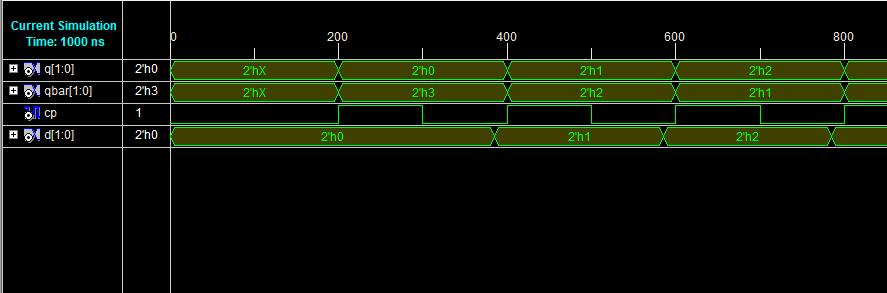
8 Figure 4: RTL schematic of Synchronous Positive edge-triggered down counter Figure 8: Internal block of synchronous positive edge-triggered up counter Table IV: Synthesis report of asynchronous positive edge-triggered up counter Figure 5: RTL schematic of Synchronous Positive edge-triggered down counter Figure 6: Technology schematic of Synchronous Positive edge-triggered down counter Figure 9: Test Bench for asynchronous positive edge-triggered up counter Figure 7: Technology schematic of synchronous positive edge-triggered up counter Figure 10: Simulated output for asynchronous positive edge-triggered up counter Page 198
9 V.CONCLUSION In this work, various architectures of MZI based functionally reversible all optical counters have been proposed. As far as our knowledge is concerned, the design of reversible all optical counter is a newer one. Our proposed design can be generalized for n-bit counter also. The proposed design techniques implement all the optical functionally reversible counters with minimum number of ancillary lines and minimum optical cost. Mathematical model has also been formulated. FUTURE WORK We can extend this project n bit counters low garbage outputs based reversible logic gates and we can also design all combinational circuits with novel reversible logic gates. REFERENCES [1] R. Landauer Irreversibility and heat generation in the computing process, IBM Journal of Research and Development, 5: , July [2] C. H. Bennett Logical reversibility of computation. IBM Journal of Logical Research and Development, 6: , November [8] B.Desoete, A.De.Vos, A reversible carry-lookahead adder using control gates, INTEGRATION the VLSI Jour. 33(1-2), (2002). [9] M. Nielsen and I. Chuang, Quantum Computation and Quantum Information, Cambridge Univ. Press, [10] C. Taraphdara, T. Chattopadhyay, and J. Roy, Mach-zehnder interferometer-based all-optical reversible logic gate, Optics and LaserTechnology, vol. 42, no. 2, pp ,2010. [11] Kotiyal, S,Thapliyal, H. and Ranganathan, N. Mach-Zehnder Interferometer Based All Optical Reversible NOR Gates. IEEE Computer Society Annual Symposium on VLSI [12] S. Kotiyal, H.Thapliyal, N. Ranganathan, Mach- Zehnder Interferometer Based Design of All Optical Reversible Binary Adder, DATE 2012, pp [13] M. Zhang, Y. Zhao, L. Wang, J. Wang, and P. Ye, Design and analysis of all-optical XOR gate using SOA-based Mach- Zehnder interferometer, Optical Communications, 223: , [3] T.Toffoli, Reversible computing, Tech. Memo- MIT/LCS/TM-151, MIT Lab for Comp. Sci, [4] C. H. Bennett, Notes on the history of reversible computation, IBM Journal of Research and Development, 32:16 23, January [5] R. Cuykendall, D.Andersen, Reversible optical computing circuits, Optics Letters 12(7), (1987). [6] R.Merkle, Reversible electronic logic using switches, Nanotechnology 4, (1993). [7] G. E. Moore Cramming more components onto integrated circuits, Electronics, 38, January Page 199
All Optical Implementation of Mach-Zehnder Interferometer Based Reversible Sequential Counters
 All Optical Implementation of Mach-Zehnder Interferometer Based Reversible Sequential Counters Jampula Prathap M.Tech Student Sri Krishna Devara Engineering College. Abstract: This work presents all optical
A Novel Approach for High Speed Performance of Sequential Circuits using Reversible Logic Based on MZI
 A Novel Approach for High Speed Performance of Sequential Circuits using Reversible Logic Based on MZI M.N.L. Prathyusha 1 G. Srujana 2 1PG Scholar, Department of ECE, Godavari Institute of Engineering
A New Gatefor Low Cost Design of All-Optical Reversible Combinational and Sequential Circuits
 A New Gatefor Low Cost Design of All-Optical Reversible Combinational and Sequential Circuits S.Manjula M.Tech Research Scholar, SNIST, Hyderabad. Dr.G.V.Maha Lakshmi Professor, SNIST, Hyderabad. Abstract:
All Optical Implementation of Mach-Zehnder Interferometer based Reversible Sequential Counters
 05 8th nternational onference 05 on 8th VLS nternational Design and onference 05 4th nternational VLS Design onference on Embedded Systems All Optical mplementation of ach-ehnder nterferometer based Reversible
A New Gate for Low Cost Design of All-optical Reversible Combinational and sequential Circuits
 A New Gate for Low Cost Design of All-optical Reversible Combinational and sequential Circuits B. Ganesh, M.Tech (VLSI-SD) Assistant Professor, Kshatriya College of Engineering. Abstract: Reversible computing
A New Gate for Low Cost Design of All-optical Reversible Logic Circuit
 A New Gate for Low Cost Design of All-optical Reversible Logic Circuit Dr.K.Srinivasulu Professor, Department of ECE, Malla Reddy College of Engineering. Abstract: The development in the field of nanometer
Efficient Reversible Multiplexer Design Using proposed All- Optical New Gate
 IOSR Journal of Electronics and Communication Engineering (IOSR-JECE) e-issn: 2278-2834,p- ISSN: 2278-8735.Volume 11, Issue 4, Ver. I (Jul.-Aug.2016), PP 45-51 www.iosrjournals.org Efficient Reversible
A New Gate for Low Cost Design of All-optical Reversible Logic Circuit
 A New Gate for Low Cost Design of All-optical Reversible Logic Circuit Mukut Bihari Malav, Department of Computer Science & Engineering UCE, Rajasthan Technical University Kota, Rajasthan, India mbmalav@gmail.com
Design of High Speed Power Efficient Combinational and Sequential Circuits Using Reversible Logic
 Design of High Speed Power Efficient Combinational and Sequential Circuits Using Reversible Logic Basthana Kumari PG Scholar, Dept. of Electronics and Communication Engineering, Intell Engineering College,
Efficient carry skip Adder design using full adder and carry skip block based on reversible Logic. India
 American Journal of Engineering Research (AJER) e-issn: 2320-0847 p-issn : 2320-0936 Volume-4, Issue-12, pp-95-100 www.ajer.org Research Paper Open Access Efficient carry skip Adder design using full adder
Contemplation of Synchronous Gray Code Counter and its Variants using Reversible Logic Gates
 Contemplation of Synchronous Gray Code Counter and its Variants using Reversible Logic Gates Rakshith Saligram Dept. of Electronics and Communication B M S College Of Engineering Bangalore, India rsaligram@gmail.com
An Area Efficient and High Speed Reversible Multiplier Using NS Gate
 RESEARCH ARTICLE OPEN ACCESS An Area Efficient and High Speed Reversible Multiplier Using NS Gate Venkateswarlu Mukku 1, Jaddu MallikharjunaReddy 2 1 Asst.Professor,Dept of ECE, Universal College Of Engineering
IMPLEMENTATION OF HIGH SPEED LOW POWER VEDIC MULTIPLIER USING REVERSIBLE LOGIC
 IMPLEMENTATION OF HIGH SPEED LOW POWER VEDIC MULTIPLIER USING REVERSIBLE LOGIC Manoj Kumar.K 1, Dr Meghana Kulkarni 2 1 PG Scholar, 2 Associate Professor Dept of PG studies, VTU-Belagavi, Karnataka,(India)
Energy Efficient Code Converters Using Reversible Logic Gates
 Energy Efficient Code Converters Using Reversible Logic Gates Gade Ujjwala MTech Student, JNIT,Hyderabad. Abstract: Reversible logic design has been one of the promising technologies gaining greater interest
A New Logic Gate for High Speed Optical Signal Processing Using Mach- Zehnder Interferometer (MZI)
") A New Logic Gate for High Speed Optical Signal Processing Using Mach- Zehnder Interferometer (MZI) Dr. Sanjeev Kumar 1, Bhushan Kumar 2, Akshay Singh 3 Assistant Professor, Department of Electronics and
A New Logic Gate for High Speed Optical Signal Processing Using Mach- Zehnder Interferometer (MZI) Dr. Sanjeev Kumar 1, Bhushan Kumar 2, Akshay Singh 3 Assistant Professor, Department of Electronics and
Design and Implementation of Reversible Multiplier using optimum TG Full Adder
 IOSR Journal of Electronics and Communication Engineering (IOSR-JECE) e-issn: 2278-2834,p- ISSN: 2278-8735.Volume 12, Issue 3, Ver. IV (May - June 2017), PP 81-89 www.iosrjournals.org Design and Implementation
FULL ADDER/SUBTRACTOR CIRCUIT USING REVERSIBLE LOGIC GATES
 FULL ADDER/SUBTRACTOR CIRCUIT USING REVERSIBLE LOGIC GATES 1 PRADEESHA R. CHANDRAN, 2 ANAND KUMAR, 3 ARTI NOOR 1 IV year, B. Tech., Dept. of ECE, Karunya University, Coimbatore, Tamil Nadu, India, 643114
Implementation of Reversible Arithmetic and Logic Unit (ALU)
") Implementation of Reversible Arithmetic and Logic Unit (ALU) G.Vimala Student, Department of Electronics and Communication Engineering, Dr K V Subba Reddy Institute of Technology, Dupadu, Kurnool,AP, India.
Implementation of Reversible Arithmetic and Logic Unit (ALU) G.Vimala Student, Department of Electronics and Communication Engineering, Dr K V Subba Reddy Institute of Technology, Dupadu, Kurnool,AP, India.
EFFICIENT DESIGN AND IMPLEMENTATION OF ADDERS WITH REVERSIBLE LOGIC
 EFFICIENT DESIGN AND IMPLEMENTATION OF ADDERS WITH REVERSIBLE LOGIC Manoj Kumar K 1, Subhash S 2, Mahesh B Neelagar 3 1,2 PG Scholar, 3 Assistant Professor, Dept of PG studies, VTU-Belagavi, Karnataka
THE USE OF SOA-BASED MACH-ZEHNDER INTERFEROMETER IN DESIGNING/IMPLEMENTING ALL OPTICAL INTEGRATED FULL ADDER-SUBTRACTOR AND DEMULTIPLEXER
 I.J.E.M.S., VOL.6 (1) 2015: 40-44 ISSN 2229-600X THE USE OF SOA-BASED MACH-ZEHNDER INTERFEROMETER IN DESIGNING/IMPLEMENTING ALL OPTICAL INTEGRATED FULL ADDER-SUBTRACTOR AND DEMULTIPLEXER 1,2 Stanley A.
High Speed Low Power Operations for FFT Using Reversible Vedic Multipliers
 High Speed Low Power Operations for FFT Using Reversible Vedic Multipliers Malugu.Divya Student of M.Tech, ECE Department (VLSI), Geethanjali College of Engineering & Technology JNTUH, India. Mrs. B. Sreelatha
Subtractor Logic Schematic
 Function Of Xor Gate In Parallel Adder Subtractor Logic Schematic metic functions, including half adder, half subtractor, full adder, independent logic gates to form desired circuits based on dif- by integrating
1. Introduction. 2. Existing Works. Volume 5 Issue 4, April Licensed Under Creative Commons Attribution CC BY
 Invert (OAI) gates are used for the skip logic and the Kogge-Stone adr is used. Kogge-stone adr is a type of pa sign is used for digital circuits. In conventional digital circuits, a significant amount
EECS150 - Digital Design Lecture 28 Course Wrap Up. Recap 1
 EECS150 - Digital Design Lecture 28 Course Wrap Up Dec. 5, 2013 Prof. Ronald Fearing Electrical Engineering and Computer Sciences University of California, Berkeley (slides courtesy of Prof. John Wawrzynek)
FPGA IMPLENTATION OF REVERSIBLE FLOATING POINT MULTIPLIER USING CSA
 FPGA IMPLENTATION OF REVERSIBLE FLOATING POINT MULTIPLIER USING CSA Vidya Devi M 1, Lakshmisagar H S 1 1 Assistant Professor, Department of Electronics and Communication BMS Institute of Technology,Bangalore
DESIGN OF REVERSIBLE MULTIPLIERS FOR LINEAR FILTERING APPLICATIONS IN DSP
 DESIGN OF REVERSIBLE MULTIPLIERS FOR LINEAR FILTERING APPLICATIONS IN DSP Rakshith Saligram 1 and Rakshith T.R 2 1 Department of Electronics and Communication, B.M.S College of Engineering, Bangalore,
Digital Electronic Concepts
 Western Technical College 10662137 Digital Electronic Concepts Course Outcome Summary Course Information Description Career Cluster Instructional Level Total Credits 4.00 Total Hours 108.00 This course
Design of 4x4 Parity Preserving Reversible Vedic Multiplier
 153 Design of 4x4 Parity Preserving Reversible Vedic Multiplier Akansha Sahu*, Anil Kumar Sahu** *(Department of Electronics & Telecommunication Engineering, CSVTU, Bhilai) ** (Department of Electronics
Performance of Optical Encoder and Optical Multiplexer Using Mach-Zehnder Switching
 RESEARCH ARTICLE OPEN ACCESS Performance of Optical Encoder and Optical Multiplexer Using Mach-Zehnder Switching Abhishek Raj 1, A.K. Jaiswal 2, Mukesh Kumar 3, Rohini Saxena 4, Neelesh Agrawal 5 1 PG
Lecture 3: Logic circuit. Combinational circuit and sequential circuit
 Lecture 3: Logic circuit Combinational circuit and sequential circuit TRAN THI HONG HONG@IS.NAIST.JP Content Lecture : Computer organization and performance evaluation metrics Lecture 2: Processor architecture
A Fault Analysis in Reversible Sequential Circuits
 IOSR Journal of VLSI and Signal Processing (IOSR-JVSP) Volume 4, Issue 2, Ver. I (Mar-Apr. 2014), PP 36-42 e-issn: 2319 4200, p-issn No. : 2319 4197 A Fault Analysis in Reversible Sequential Circuits B.Anuradha
IES Digital Mock Test
 . The circuit given below work as IES Digital Mock Test - 4 Logic A B C x y z (a) Binary to Gray code converter (c) Binary to ECESS- converter (b) Gray code to Binary converter (d) ECESS- To Gray code
Low Power Adiabatic Logic Design
 IOSR Journal of Electronics and Communication Engineering (IOSR-JECE) e-issn: 2278-2834,p- ISSN: 2278-8735.Volume 12, Issue 1, Ver. III (Jan.-Feb. 2017), PP 28-34 www.iosrjournals.org Low Power Adiabatic
TRANSISTOR LEVEL IMPLEMENTATION OF DIGITAL REVERSIBLE CIRCUITS
 TRANSISTOR LEVEL IMPLEMENTATION OF DIGITAL REVERSIBLE CIRCUITS K.Prudhvi Raj 1 and Y.Syamala 2 1 PG student, Gudlavalleru Engineering College, Krishna district, Andhra Pradesh, India 2 Departement of ECE,
Design of a Power Optimal Reversible FIR Filter ASIC Speech Signal Processing
 Design of a Power Optimal Reversible FIR Filter ASIC Speech Signal Processing Yelle Harika M.Tech, Joginpally B.R.Engineering College. P.N.V.M.Sastry M.S(ECE)(A.U), M.Tech(ECE), (Ph.D)ECE(JNTUH), PG DIP
Module -18 Flip flops
 1 Module -18 Flip flops 1. Introduction 2. Comparison of latches and flip flops. 3. Clock the trigger signal 4. Flip flops 4.1. Level triggered flip flops SR, D and JK flip flops 4.2. Edge triggered flip
INTERNATIONAL JOURNAL OF APPLIED ENGINEERING RESEARCH, DINDIGUL Volume 1, No 3, 2010
 All Optical Half Adder Design Using Equations Governing XGM and FWM Effect in Semiconductor Optical Amplifier V. K. Srivastava, V. Priye Indian School of Mines University, Dhanbad srivastavavikrant@hotmail.com
Design of high speed multiplier using Modified Booth Algorithm with hybrid carry look-ahead adder
 Design of high speed multiplier using Modified Booth Algorithm with hybrid carry look-ahead adder Balakumaran R, Department of Electronics and Communication Engineering, Amrita School of Engineering, Coimbatore,
A Novel Low-Power Reversible Vedic Multiplier
 A Novel Low-Power Reversible Vedic Multiplier [1] P.Kiran Kumar, [2] E.Padmaja Research Scholar in ECE, KL University Asst. Professor in ECE, Balaji Institute of Technology and Science Abstract - In reversible
COMBINATIONAL and SEQUENTIAL LOGIC CIRCUITS Hardware implementation and software design
 PH-315 COMINATIONAL and SEUENTIAL LOGIC CIRCUITS Hardware implementation and software design A La Rosa I PURPOSE: To familiarize with combinational and sequential logic circuits Combinational circuits
All Optical Universal logic Gates Design and Simulation using SOA
 International Journal of Computational Engineering & Management, Vol. 15 Issue 1, January 2012 www..org 41 All Optical Universal logic Gates Design and Simulation using SOA Rekha Mehra 1, J. K. Tripathi
Performance Analysis of SOA-MZI based All-Optical AND & XOR Gate
 International Journal of Current Engineering and Technology E-ISSN 2277 4106, P-ISSN 2347 5161 2016 INPRESSCO, All Rights Reserved Available at http://inpressco.com/category/ijcet Research Article Utkarsh
High Speed and Low Power Multiplier Using Reversible Logic for Wireless Communications
 International Journal of Emerging Engineering Research and Technology Volume 3, Issue 8, August 2015, PP 62-69 ISSN 2349-4395 (Print) & ISSN 2349-4409 (Online) High Speed and Low Power Multiplier Using
Design and Implementation of High Speed Carry Select Adder Korrapatti Mohammed Ghouse 1 K.Bala. 2
 IJSRD - International Journal for Scientific Research & Development Vol. 3, Issue 07, 2015 ISSN (online): 2321-0613 Design and Implementation of High Speed Carry Select Adder Korrapatti Mohammed Ghouse
Fpga Implementation of Truncated Multiplier Using Reversible Logic Gates
 International Journal of Engineering Science Invention ISSN (Online): 2319 6734, ISSN (Print): 2319 6726 Volume 2 Issue 12 ǁ December. 2013 ǁ PP.44-48 Fpga Implementation of Truncated Multiplier Using
Number system: the system used to count discrete units is called number. Decimal system: the number system that contains 10 distinguished
 Number system: the system used to count discrete units is called number system Decimal system: the number system that contains 10 distinguished symbols that is 0-9 or digits is called decimal system. As
Design and Implementation of Complex Multiplier Using Compressors
 Design and Implementation of Complex Multiplier Using Compressors Abstract: In this paper, a low-power high speed Complex Multiplier using compressor circuit is proposed for fast digital arithmetic integrated
Course Outcome of M.Tech (VLSI Design)
") Course Outcome of M.Tech (VLSI Design) PVL108: Device Physics and Technology The students are able to: 1. Understand the basic physics of semiconductor devices and the basics theory of PN junction. 2.
Course Outcome of M.Tech (VLSI Design) PVL108: Device Physics and Technology The students are able to: 1. Understand the basic physics of semiconductor devices and the basics theory of PN junction. 2.
Efficient Reversible GVJ Gate as Half Adder & Full Adder and its Testing on Single Precision Floating Point Multiplier
 Efficient Reversible GVJ Gate as Half Adder & Full Adder and its Testing on Single Precision Floating Point Multiplier Efficient Reversible GVJ Gate as Half Adder & Full Adder and its Testing on Single
R.B.V.R.R. WOMEN S COLLEGE (AUTONOMOUS) Narayanaguda, Hyderabad. ELECTRONIC PRINCIPLES AND APPLICATIONS
 Narayanaguda, Hyderabad. ELECTRONIC PRINCIPLES AND APPLICATIONS") R.B.V.R.R. WOMEN S COLLEGE (AUTONOMOUS) Narayanaguda, Hyderabad. DEPARTMENT OF PHYSICS QUESTION BANK FOR SEMESTER V PHYSICS PAPER VI (A) ELECTRONIC PRINCIPLES AND APPLICATIONS UNIT I: SEMICONDUCTOR DEVICES
R.B.V.R.R. WOMEN S COLLEGE (AUTONOMOUS) Narayanaguda, Hyderabad. DEPARTMENT OF PHYSICS QUESTION BANK FOR SEMESTER V PHYSICS PAPER VI (A) ELECTRONIC PRINCIPLES AND APPLICATIONS UNIT I: SEMICONDUCTOR DEVICES
A Novel Design of High-Speed Carry Skip Adder Operating Under a Wide Range of Supply Voltages
 A Novel Design of High-Speed Carry Skip Adder Operating Under a Wide Range of Supply Voltages Jalluri srinivisu,(m.tech),email Id: jsvasu494@gmail.com Ch.Prabhakar,M.tech,Assoc.Prof,Email Id: skytechsolutions2015@gmail.com
Brought to you by. Priti Srinivas Sajja. PS01CMCA02 Course Content. Tutorial Practice Material. Acknowldgement References. Website pritisajja.
 Brought to you by Priti Srinivas Sajja PS01CMCA02 Course Content Tutorial Practice Material Acknowldgement References Website pritisajja.info Multiplexer Means many into one, also called data selector
EFFICIENT REVERSIBLE MULTIPLIER CIRCUIT IMPLEMENTATION IN FPGA
 EFFICIENT REVERSIBLE MULTIPLIER CIRCUIT IMPLEMENTATION IN FPGA Kamatham Harikrishna Department of Electronics and Communication Engineering, Vardhaman College of Engineering, Shamshabad, Hyderabad, AP,
Synthesis of Balanced Quaternary Reversible Logic Circuit
 Synthesis of alanced Quaternary Reversible Logic Circuit Jitesh Kumar Meena jiteshmeena8@gmail.com Sushil Chandra Jain scjain1@yahoo.com Hitesh Gupta hiteshnice@gmail.com Shubham Gupta guptashubham396@gmail.com
A COMPARATIVE ANALYSIS OF AN ULTRA-LOW VOLTAGE 1-BIT FULL SUBTRACTOR DESIGNED IN BOTH DIGITAL AND ANALOG ENVIRONMENTS
 A COMPARATIVE ANALYSIS OF AN ULTRA-LOW VOLTAGE 1-BIT FULL SUBTRACTOR DESIGNED IN BOTH DIGITAL AND ANALOG ENVIRONMENTS Suchismita Sengupta M.Tech Student, VLSI & EMBEDDED Systems, Dept. Of Electronics &
An Efficient SQRT Architecture of Carry Select Adder Design by HA and Common Boolean Logic PinnikaVenkateswarlu 1, Ragutla Kalpana 2
 An Efficient SQRT Architecture of Carry Select Adder Design by HA and Common Boolean Logic PinnikaVenkateswarlu 1, Ragutla Kalpana 2 1 M.Tech student, ECE, Sri Indu College of Engineering and Technology,
REALIZATION OF VEDIC MULTIPLIER USING URDHVA - TIRYAKBHAYAM SUTRAS
 REALIZATION OF VEDIC MULTIPLIER USING URDHVA - TIRYAKBHAYAM SUTRAS, 1 PG Scholar, VAAGDEVI COLLEGE OF ENGINEERING, Warangal, Telangana. 2 Assistant Professor, VAAGDEVI COLLEGE OF ENGINEERING, Warangal,Telangana.
Design and Analysis of f2g Gate using Adiabatic Technique
 Design and Analysis of f2g Gate using Adiabatic Technique Renganayaki. G 1, Thiyagu.P 2 1, 2 K.C.G College of Technology, Electronics and Communication, Karapakkam,Chennai-600097, India Abstract: This
A NOVEL APPROACH OF VEDIC MATHEMATICS USING REVERSIBLE LOGIC FOR HIGH SPEED ASIC DESIGN OF COMPLEX MULTIPLIER
 A NOVEL APPROACH OF VEDIC MATHEMATICS USING REVERSIBLE LOGIC FOR HIGH SPEED ASIC DESIGN OF COMPLEX MULTIPLIER SK. MASTAN VALI 1*, N.SATYANARAYAN 2* 1. II.M.Tech, Dept of ECE, AM Reddy Memorial College
Code No: R Set No. 1
 Code No: R05310402 Set No. 1 1. (a) What are the parameters that are necessary to define the electrical characteristics of CMOS circuits? Mention the typical values of a CMOS NAND gate. (b) Design a CMOS
Design of Low Power Flip Flop Based on Modified GDI Primitive Cells and Its Implementation in Sequential Circuits
 Design of Low Power Flip Flop Based on Modified GDI Primitive Cells and Its Implementation in Sequential Circuits Dr. Saravanan Savadipalayam Venkatachalam Principal and Professor, Department of Mechanical
FPGA Implementation of Fast and Power Efficient 4 Bit Vedic Multiplier (Urdhva Tiryakbhayam) using Reversible Logical Gate
 using Reversible Logical Gate") 34 FPGA Implementation of Fast and Power Efficient 4 Bit Vedic Multiplier (Urdhva Tiryakbhayam) using Reversible Logical Gate Sainadh chintha, M.Tech VLSI Group, Dept. of ECE, Nova College of Engineering
34 FPGA Implementation of Fast and Power Efficient 4 Bit Vedic Multiplier (Urdhva Tiryakbhayam) using Reversible Logical Gate Sainadh chintha, M.Tech VLSI Group, Dept. of ECE, Nova College of Engineering
DAV Institute of Engineering & Technology Department of ECE. Course Outcomes
 DAV Institute of Engineering & Technology Department of ECE Course Outcomes Upon successful completion of this course, the student will intend to apply the various outcome as:: BTEC-301, Analog Devices
Fan in: The number of inputs of a logic gate can handle.
 Subject Code: 17333 Model Answer Page 1/ 29 Important Instructions to examiners: 1) The answers should be examined by key words and not as word-to-word as given in the model answer scheme. 2) The model
All Optical Binary Divider
 International Journal of Optics and Applications 2012, 2(1): 2226 DOI: 10.5923/j.optics.20120201.03 All Optical Binary Divider Tamer A. Moniem Faculty of engineering, MSA, CairoEgypt Abstract This paper
Area Delay Efficient Novel Adder By QCA Technology
 Area Delay Efficient Novel Adder By QCA Technology 1 Mohammad Mahad, 2 Manisha Waje 1 Research Student, Department of ETC, G.H.Raisoni College of Engineering, Pune, India 2 Assistant Professor, Department
An Efficient Method for Implementation of Convolution
 IAAST ONLINE ISSN 2277-1565 PRINT ISSN 0976-4828 CODEN: IAASCA International Archive of Applied Sciences and Technology IAAST; Vol 4 [2] June 2013: 62-69 2013 Society of Education, India [ISO9001: 2008
COMPUTER ORGANIZATION & ARCHITECTURE DIGITAL LOGIC CSCD211- DEPARTMENT OF COMPUTER SCIENCE, UNIVERSITY OF GHANA
 COMPUTER ORGANIZATION & ARCHITECTURE DIGITAL LOGIC LOGIC Logic is a branch of math that tries to look at problems in terms of being either true or false. It will use a set of statements to derive new true
Implementation of an 8-bit Low-power Multiplier based on Reversible Gate Technology
 SEE 2014 Zone I Conference, pril 3-5, 2014, University of ridgeport, ridgpeort, CT, US. Implementation of an 8-bit Low-power Multiplier based on Reversible Gate Technology orui Li 1, Xiaowei Yu 2, o Zhang
SYLLABUS of the course BASIC ELECTRONICS AND DIGITAL SIGNAL PROCESSING. Master in Computer Science, University of Bolzano-Bozen, a.y.
 SYLLABUS of the course BASIC ELECTRONICS AND DIGITAL SIGNAL PROCESSING Master in Computer Science, University of Bolzano-Bozen, a.y. 2017-2018 Lecturer: LEONARDO RICCI (last updated on November 27, 2017)
Gates and Circuits 1
 1 Gates and Circuits Chapter Goals Identify the basic gates and describe the behavior of each Describe how gates are implemented using transistors Combine basic gates into circuits Describe the behavior
IN the past few years, superconductor-based logic families
 1 Synthesis Flow for Cell-Based Adiabatic Quantum-Flux-Parametron Structural Circuit Generation with HDL Backend Verification Qiuyun Xu, Christopher L. Ayala, Member, IEEE, Naoki Takeuchi, Member, IEEE,
[Krishna, 2(9): September, 2013] ISSN: Impact Factor: INTERNATIONAL JOURNAL OF ENGINEERING SCIENCES & RESEARCH TECHNOLOGY
![[Krishna, 2(9): September, 2013] ISSN: Impact Factor: INTERNATIONAL JOURNAL OF ENGINEERING SCIENCES & RESEARCH TECHNOLOGY](/thumbs/77/74980115.jpg "[Krishna, 2(9): September, 2013] ISSN: Impact Factor: INTERNATIONAL JOURNAL OF ENGINEERING SCIENCES & RESEARCH TECHNOLOGY") IJESRT INTERNATIONAL JOURNAL OF ENGINEERING SCIENCES & RESEARCH TECHNOLOGY Design of Wallace Tree Multiplier using Compressors K.Gopi Krishna *1, B.Santhosh 2, V.Sridhar 3 gopikoleti@gmail.com Abstract
IJESRT INTERNATIONAL JOURNAL OF ENGINEERING SCIENCES & RESEARCH TECHNOLOGY Design of Wallace Tree Multiplier using Compressors K.Gopi Krishna *1, B.Santhosh 2, V.Sridhar 3 gopikoleti@gmail.com Abstract
Module-20 Shift Registers
 1 Module-20 Shift Registers 1. Introduction 2. Types of shift registers 2.1 Serial In Serial Out (SISO) register 2.2 Serial In Parallel Out (SIPO) register 2.3 Parallel In Parallel Out (PIPO) register
ISSN Vol.02, Issue.11, December-2014, Pages:
 ISSN 2322-0929 Vol.02, Issue.11, December-2014, Pages:1134-1139 www.ijvdcs.org Optimized Reversible Vedic Multipliers for High Speed Low Power Operations GOPATHOTI VINOD KUMAR 1, KANDULA RAVI KUMAR 2,
Low Power FIR Filter Structure Design Using Reversible Logic Gates for Speech Signal Processing
 Low Power FIR Filter Structure Design Using Reversible Logic Gates for Speech Signal Processing V.Laxmi Prasanna M.Tech, 14Q96D7714 Embedded Systems and VLSI, Malla Reddy College of Engineering. M.Chandra
CS302 - Digital Logic Design Glossary By
 CS302 - Digital Logic Design Glossary By ABEL : Advanced Boolean Expression Language; a software compiler language for SPLD programming; a type of hardware description language (HDL) Adder : A digital
Power Optimized Energy Efficient Hybrid Circuits Design by Using A Novel Adiabatic Techniques N.L.S.P.Sai Ram*, K.Rajasekhar**
 Power Optimized Energy Efficient Hybrid Circuits Design by Using A Novel Adiabatic Techniques N.L.S.P.Sai Ram*, K.Rajasekhar** *(Department of Electronics and Communication Engineering, ASR College of
DIGITAL INTEGRATED CIRCUITS A DESIGN PERSPECTIVE 2 N D E D I T I O N
 DIGITAL INTEGRATED CIRCUITS A DESIGN PERSPECTIVE 2 N D E D I T I O N Jan M. Rabaey, Anantha Chandrakasan, and Borivoje Nikolic CONTENTS PART I: THE FABRICS Chapter 1: Introduction (32 pages) 1.1 A Historical
A High Performance Asynchronous Counter using Area and Power Efficient GDI T-Flip Flop
 Indian Journal of Science and Technology, Vol 8(7), 622 628, April 2015 ISSN (Print) : 0974-6846 ISSN (Online) : 0974-5645 DOI: 10.17485/ijst/2015/v8i7/62847 A High Performance Asynchronous Counter using
CHAPTER III THE FPGA IMPLEMENTATION OF PULSE WIDTH MODULATION
 34 CHAPTER III THE FPGA IMPLEMENTATION OF PULSE WIDTH MODULATION 3.1 Introduction A number of PWM schemes are used to obtain variable voltage and frequency supply. The Pulse width of PWM pulsevaries with
SIGNED PIPELINED MULTIPLIER USING HIGH SPEED COMPRESSORS
 INTERNATIONAL JOURNAL OF RESEARCH IN COMPUTER APPLICATIONS AND ROBOTICS ISSN 2320-7345 SIGNED PIPELINED MULTIPLIER USING HIGH SPEED COMPRESSORS 1 T.Thomas Leonid, 2 M.Mary Grace Neela, and 3 Jose Anand
FPGA Realization of Hybrid Carry Select-cum- Section-Carry Based Carry Lookahead Adders
 FPGA Realization of Hybrid Carry Select-cum- Section-Carry Based Carry Lookahead s V. Kokilavani Department of PG Studies in Engineering S. A. Engineering College (Affiliated to Anna University) Chennai
An Optimized Wallace Tree Multiplier using Parallel Prefix Han-Carlson Adder for DSP Processors
 An Optimized Wallace Tree Multiplier using Parallel Prefix Han-Carlson Adder for DSP Processors T.N.Priyatharshne Prof. L. Raja, M.E, (Ph.D) A. Vinodhini ME VLSI DESIGN Professor, ECE DEPT ME VLSI DESIGN
ISSN (PRINT): , (ONLINE): , VOLUME-3, ISSUE-8,
: , (ONLINE): , VOLUME-3, ISSUE-8,") DESIGN OF SEQUENTIAL CIRCUITS USING MULTI-VALUED LOGIC BASED ON QDGFET Chetan T. Bulbule 1, S. S. Narkhede 2 Department of E&TC PICT Pune India chetanbulbule7@gmail.com 1, ssn_pict@yahoo.com 2 Abstract
DESIGN OF SEQUENTIAL CIRCUITS USING MULTI-VALUED LOGIC BASED ON QDGFET Chetan T. Bulbule 1, S. S. Narkhede 2 Department of E&TC PICT Pune India chetanbulbule7@gmail.com 1, ssn_pict@yahoo.com 2 Abstract
Design of low power delay efficient Vedic multiplier using reversible gates
 ISSN: 2454-132X Impact factor: 4.295 (Volume 4, Issue 3) Available online at: www.ijariit.com Design of low power delay efficient Vedic multiplier using reversible gates B Ramya bramyabrbg9741@gmail.com
High Speed Binary Counters Based on Wallace Tree Multiplier in VHDL
 High Speed Binary Counters Based on Wallace Tree Multiplier in VHDL E.Sangeetha 1 ASP and D.Tharaliga 2 Department of Electronics and Communication Engineering, Tagore College of Engineering and Technology,
Design of Modified Shannon Based Full Adder Cell Using PTL Logic for Low Power Applications
 Design of Modified Shannon Based Full Adder Cell Using PTL Logic for Low Power Applications K.Purnima #1, S.AdiLakshmi #2, M.Sahithi #3, A.Jhansi Rani #4,J.Poornima #5 #1 M.Tech student, Department of
Digital Electronics Course Objectives
 Digital Electronics Course Objectives In this course, we learning is reported using Standards Referenced Reporting (SRR). SRR seeks to provide students with grades that are consistent, are accurate, and
Gates and and Circuits
 Chapter 4 Gates and Circuits Chapter Goals Identify the basic gates and describe the behavior of each Describe how gates are implemented using transistors Combine basic gates into circuits Describe the
VCO Based Injection-Locked Clock Multiplier with a Continuous Frequency Tracking Loop
 IOSR Journal of Electronics and Communication Engineering (IOSR-JECE) e-issn: 2278-2834,p- ISSN: 2278-8735.Volume 13, Issue 4, Ver. I (Jul.-Aug. 2018), PP 26-30 www.iosrjournals.org VCO Based Injection-Locked
Berger Checks and Fault Tolerant Reversible Arithmetic Component Design
 Berger Checks and Fault Tolerant Reversible Arithmetic Component Design Uppara Rajesh PG Scholar, Sri Krishnadevaraya Engineering College, Gooty, AP, India. E.Ramakrishna Naik Assistant Professor, Sri
ISSN Vol.03, Issue.07, September-2015, Pages:
 ISSN 2322-0929 Vol.03, Issue.07, September-2015, Pages:1116-1121 www.ijvdcs.org Design and Implementation of 32-Bits Carry Skip Adder using CMOS Logic in Virtuoso, Cadence ISHMEET SINGH 1, MANIKA DHINGRA
MODIFIED BOOTH ALGORITHM FOR HIGH SPEED MULTIPLIER USING HYBRID CARRY LOOK-AHEAD ADDER
 MODIFIED BOOTH ALGORITHM FOR HIGH SPEED MULTIPLIER USING HYBRID CARRY LOOK-AHEAD ADDER #1 K PRIYANKA, #2 DR. M. RAMESH BABU #1,2 Department of ECE, #1,2 Institute of Aeronautical Engineering, Hyderabad,Telangana,
MAHARASHTRA STATE BOARD OF TECHNICAL EDUCATION (Autonomous) (ISO/IEC Certified) SUMMER-16 EXAMINATION Model Answer
 (ISO/IEC Certified) SUMMER-16 EXAMINATION Model Answer") Important Instructions to examiners: 1) The answers should be examined by key words and not as word-to-word as given in the model answer scheme. 2) The model answer and the answer written by candidate
Important Instructions to examiners: 1) The answers should be examined by key words and not as word-to-word as given in the model answer scheme. 2) The model answer and the answer written by candidate
A Novel Approach to Design 2-bit Binary Arithmetic Logic Unit (ALU) Circuit Using Optimized 8:1 Multiplexer with Reversible logic
 Circuit Using Optimized 8:1 Multiplexer with Reversible logic") 4 JOURNAL OF COMMUNICATIONS SOFTWARE AND SYSTEMS, VOL., NO. 2, JUNE 25 A Novel Approach to Design 2-bit Binary Arithmetic Logic Unit (ALU) Circuit Using Optimized 8: Multiplexer with Reversible logic Vandana
4 JOURNAL OF COMMUNICATIONS SOFTWARE AND SYSTEMS, VOL., NO. 2, JUNE 25 A Novel Approach to Design 2-bit Binary Arithmetic Logic Unit (ALU) Circuit Using Optimized 8: Multiplexer with Reversible logic Vandana
EEE 301 Digital Electronics
 EEE 301 Digital Electronics Lecture 1 Course Contents Introduction to number systems and codes. Analysis and synthesis of digital logic circuits: Basic logic functions, Boolean algebra,combinational logic
V-LAB COMPUTER INTERFACED TRAINING SET
 is an important tool for Vocational Education with it s built-in measurement units and signal generators that are interfaced with computer for control and measurement. is a device for real-time measurement
Objective Questions. (a) Light (b) Temperature (c) Sound (d) all of these
 Light (b) Temperature (c) Sound (d) all of these") Objective Questions Module 1: Introduction 1. Which of the following is an analog quantity? (a) Light (b) Temperature (c) Sound (d) all of these 2. Which of the following is a digital quantity? (a) Electrical
Objective Questions Module 1: Introduction 1. Which of the following is an analog quantity? (a) Light (b) Temperature (c) Sound (d) all of these 2. Which of the following is a digital quantity? (a) Electrical
COMPARISION OF LOW POWER AND DELAY USING BAUGH WOOLEY AND WALLACE TREE MULTIPLIERS
 COMPARISION OF LOW POWER AND DELAY USING BAUGH WOOLEY AND WALLACE TREE MULTIPLIERS ( 1 Dr.V.Malleswara rao, 2 K.V.Ganesh, 3 P.Pavan Kumar) 1 Professor &HOD of ECE,GITAM University,Visakhapatnam. 2 Ph.D