CHAPTER 11. Feedback. Microelectronic Circuits, Seventh Edition. Copyright 2015 by Oxford University Press
|
|
|
- Lucas Eaton
- 6 years ago
- Views:
Transcription
1 CHAPTER 11 Feedback

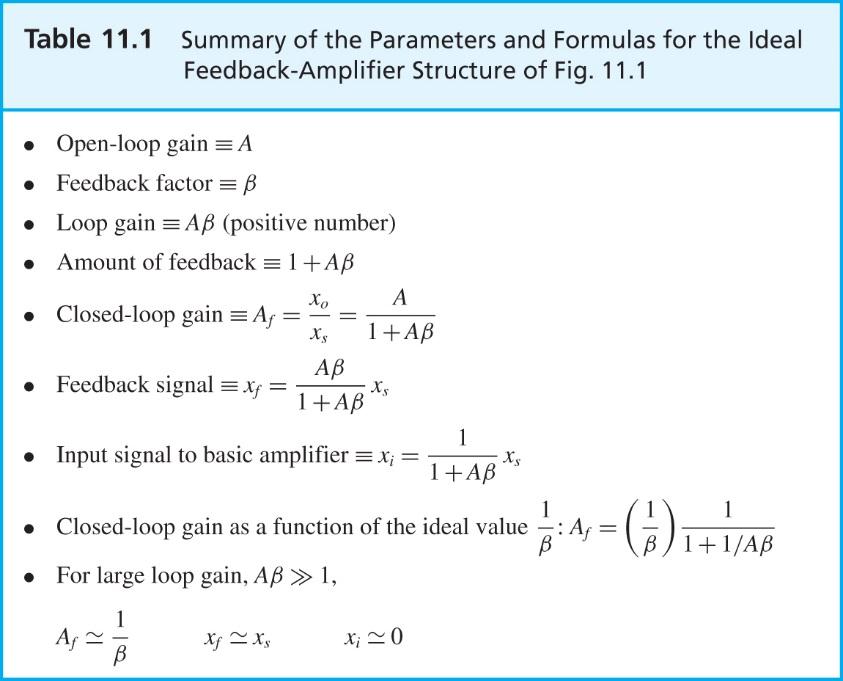
2 Figure 11.1 General structure of the feedback amplifier. This is a signal-flow diagram, and the quantities x represent either voltage or current signals.

3 Figure 11.2 Determining the loop gain by breaking the feedback loop at the output of the basic amplifier, applying a test signal xt, and measuring the returned signal xr : Aβ xr/xt.
 A noninverting op-amp circuit for Example 11")
4 Figure 11.3 (a) A noninverting op-amp circuit for Example (b) The circuit in (a) with the op amp replaced with its equivalent circuit.
5
6 Figure 11.4 Application of negative feedback reduces the midband gain, increases fh, and reduces fl, all by the same factor, (1 + AMβ), which is equal to the amount of feedback.
7 Figure 11.5 Illustrating the application of negative feedback to improve the signal-to-interference ratio in amplifiers.
8
9 Figure 11.7 Block diagram of a feedback voltage amplifier. Here the appropriate feedback topology is series shunt.

10 Figure 11.8 Examples of a feedback voltage amplifier. All these circuits employ series shunt feedback. Note that the dc bias circuits are only partially shown.
11 Figure 11.9 Breaking the conceptual feedback loop in (a) to determine the loop gain requires the termination of the loop as shown in (b), to ensure that the loop conditions do not change.
12 Figure Determining: (a) the feedback factor β; and (b) the loop gain Aβ for the feedback voltage amplifier of Fig. 11.8(b).
 A series shunt feedback amplifier; (b) the feedback loop obtained by setting Vs = 0 and replacing the op amp with its")
13 Figure Example (a) A series shunt feedback amplifier; (b) the feedback loop obtained by setting Vs = 0 and replacing the op amp with its equivalent-circuit model; (c) breaking the feedback loop to determine the loop gain Aβ = Vr/Vt.

")
14 Figure The series shunt feedback amplifier: (a) ideal structure; (b) equivalent circuit.
15 Figure Determining the output resistance of the feedback amplifier of Fig (a): Rof = Vx/Ix.
 Block diagram of a practical series shunt feedback amplifier.")
. (c) Definition of R11 and R22.")
16 Figure (a) Block diagram of a practical series shunt feedback amplifier. (b) The circuit in (a) represented by the ideal structure of Fig (a). (c) Definition of R11 and R22. (d) Determination of the feedback factor β. (e) The A circuit, showing the open-loop resistances Ri and Ro.
17 Figure continued


18 Figure Circuits for Example 11.4.
 Series shunt feedback amplifier for Example")
19 Figure (a) Series shunt feedback amplifier for Example 11.5; (b) the A circuit; (c) the β circuit.
20 Figure E11.8
21 Figure Example 11.6.


22 Figure The feedback transconductance amplifier (series series).
23 Figure The feedback transconductance amplifier (series series).
24 Figure Circuits for Example 11.7.

25 Figure Circuits for Example 11.8.


26 Figure The feedback transresistance amplifier (shunt shunt).
27 Figure The feedback transresistance amplifier (shunt shunt).
28 Figure (a) A feedback transresistance amplifier; (b) the β circuit; (c) determining β; (d) the A circuit.
29 Figure E11.19


30 Figure The feedback current amplifier (shunt series).
31 Figure The feedback current amplifier (shunt series).
32 Figure Circuit for Example
33 Figure continued
34
35 Figure The Nyquist plot of an unstable amplifier.
36 Figure Relationship between pole location and transient response.
37 Figure Effect of feedback on (a) the pole location and (b) the frequency response of an amplifier having a single-pole, open-loop response.
38 Figure Root-locus diagram for a feedback amplifier whose open-loop transfer function has two real poles.
39 Figure Definition of ω0 and Q of a pair of complex-conjugate poles.
40 Figure Normalized gain of a two-pole feedback amplifier for various values of Q. Note that Q is determined by the loop gain according to Eq. (11.70).


41 Figure Circuits and plot for Example
42 Figure Root-locus diagram for an amplifier with three poles. The arrows indicate the pole movement as A0β is increased.
43 Figure E11.26
44 Figure Bode plot for the loop gain Aβ illustrating the definitions of the gain and phase margins.
45 Figure Stability analysis using Bode plot of A.
46
47 Figure (a) Two cascaded gain stages of a multistage amplifier. (b) Equivalent circuit for the interface between the two stages in (a). (c) Same circuit as in (b), but with a compensating capacitor CC added. Note that the analysis here applies equally well to MOS amplifiers.
48 Figure (a) A gain stage in a multistage amplifier with a compensating capacitor connected in the feedback path, and (b) equivalent circuit. Note that although a BJT is shown, the analysis applies equally well to the MOSFET case.

49 Figure P11.2
50 Figure P11.3

51 Figure P11.9
52 Figure P11.24
53 Figure P11.29
54 Figure P11.31
55 Figure P11.32
56 Figure P11.33
57 Figure P11.40
58 Figure P11.41
59 Figure P11.43
60 Figure P11.45
61 Figure P11.47
62 Figure P11.48
63 Figure P11.52
64 Figure P11.53
65 Figure P11.54
66 Figure P11.55
67 Figure P11.56
68 Figure P11.57
69 Figure P11.58
70 Figure P11.63
71 Figure P11.64
72 Figure P11.65
73 Figure P11.68
74 Figure P11.69
75 Figure P11.70
76 Figure P11.72
77 Figure P11.73
78 Figure P11.77
79 Figure P11.78
80 Figure P11.79
81 Figure P11.80
82 Figure P11.81
83 Figure P11.82
84 Figure P11.106
Microelectronic Circuits - Fifth Edition Sedra/Smith Copyright 2004 by Oxford University Press, Inc.
 Feedback 1 Figure 8.1 General structure of the feedback amplifier. This is a signal-flow diagram, and the quantities x represent either voltage or current signals. 2 Figure E8.1 3 Figure 8.2 Illustrating
CHAPTER 9 FEEDBACK. NTUEE Electronics L.H. Lu 9-1
 CHAPTER 9 FEEDBACK Chapter Outline 9.1 The General Feedback Structure 9.2 Some Properties of Negative Feedback 9.3 The Four Basic Feedback Topologies 9.4 The Feedback Voltage Amplifier (Series-Shunt) 9.5
Chapter 10 Feedback ECE 3120 Microelectronics II Dr. Suketu Naik
 1 Chapter 10 Feedback Operational Amplifier Circuit Components 2 1. Ch 7: Current Mirrors and Biasing 2. Ch 9: Frequency Response 3. Ch 8: Active-Loaded Differential Pair 4. Ch 10: Feedback 5. Ch 11: Output
Microelectronic Circuits. Feedback Amplifiers. Slide 1. Lecture on Microelectronics Circuits. BITS Pilani, Dubai Campus. Dr. Vilas
 Microelectronic Circuits Feedback mplifiers Slide 1 General Structure of Feedback Comparison Circuit / Mixer x o = x i ; x f = b x o ; x i = x s - x f ; f = (x o /x s ) = / (1+b). lso, x f = bx s / (1+b)
Homework Assignment 10
 Homework Assignment 10 Question The amplifier below has infinite input resistance, zero output resistance and an openloop gain. If, find the value of the feedback factor as well as so that the closed-loop
Microelectronic Circuits II. Ch 9 : Feedback
 Microelectronic Circuits II Ch 9 : Feedback 9.9 Determining the Loop Gain 9.0 The Stability problem 9. Effect on Feedback on the Amplifier Poles 9.2 Stability study using Bode plots 9.3 Frequency Compensation
Example #6 1. An amplifier with a nominal gain
 1. An amplifier with a nominal gain A=1000 V/V exhibits a gain change of 10% as the operating temperature changes from 25 o C to 75 o C. If it is required to constrain the change to 0.1% by applying negative
PURPOSE: NOTE: Be sure to record ALL results in your laboratory notebook.
 EE4902 Lab 9 CMOS OP-AMP PURPOSE: The purpose of this lab is to measure the closed-loop performance of an op-amp designed from individual MOSFETs. This op-amp, shown in Fig. 9-1, combines all of the major
Homework Assignment 13
 Question 1 Short Takes 2 points each. Homework Assignment 13 1. Classify the type of feedback uses in the circuit below (i.e., shunt-shunt, series-shunt, ) 2. True or false: an engineer uses series-shunt
You will be asked to make the following statement and provide your signature on the top of your solutions.
 1 EE 435 Name Exam 1 Spring 216 Instructions: The points allocated to each problem are as indicated. Note that the first and last problem are weighted more heavily than the rest of the problems. On those
or Op Amps for short
 or Op Amps for short Objective of Lecture Describe how an ideal operational amplifier (op amp) behaves. Chapter 14.1 Electrical Engineering: Principles and Applications Chapter 5.1-5.3 Fundamentals of
Index. Small-Signal Models, 14 saturation current, 3, 5 Transistor Cutoff Frequency, 18 transconductance, 16, 22 transit time, 10
 Index A absolute value, 308 additional pole, 271 analog multiplier, 190 B BiCMOS,107 Bode plot, 266 base-emitter voltage, 16, 50 base-emitter voltages, 296 bias current, 111, 124, 133, 137, 166, 185 bipolar
Microelectronic Circuits
 SECOND EDITION ISHBWHBI \ ' -' Microelectronic Circuits Adel S. Sedra University of Toronto Kenneth С Smith University of Toronto HOLT, RINEHART AND WINSTON HOLT, RINEHART AND WINSTON, INC. New York Chicago
EXP8: AMPLIFIERS II.
 EXP8: AMPLIFIES II. Objectives. The objectives of this lab are:. To analyze the behavior of a class A amplifier. 2. To understand the role the components play in the gain of the circuit. 3. To find the
Reading. Lecture 33: Context. Lecture Outline. Chapter 9, multi-stage amplifiers. Prof. J. S. Smith
 eading Lecture 33: Chapter 9, multi-stage amplifiers Prof J. S. Smith Context Lecture Outline We are continuing to review some of the building blocks for multi-stage amplifiers, including current sources
EE 435. Lecture 16. Compensation Systematic Two-Stage Op Amp Design
 EE 435 Lecture 16 Compensation Systematic Two-Stage Op Amp Design Review from last lecture Review of Basic Concepts Pole Locations and Stability Theorem: A system is stable iff all closed-loop poles lie
CMOS Operational-Amplifier
 CMOS Operational-Amplifier 1 What will we learn in this course How to design a good OP Amp. Basic building blocks Biasing and Loading Swings and Bandwidth CH2(8) Operational Amplifier as A Black Box Copyright
Chapter #12: Feedback. Eng.Mohammed S. Abuwarda. Fall Semester_2017
 Chapter #12: Feedback Eng.Mohammed S. Abuwarda Fall Semester_2017 10.1. The General Feedback Structure Figure 10.1. shows the basic structure of a feedback amplifier signal-flow diagram. Open-loop amplifier
Lecture 33: Context. Prof. J. S. Smith
 Lecture 33: Prof J. S. Smith Context We are continuing to review some of the building blocks for multi-stage amplifiers, including current sources and cascode connected devices, and we will also look at
CMOS Operational-Amplifier
 CMOS Operational-Amplifier 1 What will we learn in this course How to design a good OP Amp. Basic building blocks Biasing and Loading Swings and Bandwidth CH2(8) Operational Amplifier as A Black Box Copyright
BJT Circuits (MCQs of Moderate Complexity)
") BJT Circuits (MCQs of Moderate Complexity) 1. The current ib through base of a silicon npn transistor is 1+0.1 cos (1000πt) ma. At 300K, the rπ in the small signal model of the transistor is i b B C r
BJT Circuits (MCQs of Moderate Complexity) 1. The current ib through base of a silicon npn transistor is 1+0.1 cos (1000πt) ma. At 300K, the rπ in the small signal model of the transistor is i b B C r
GOPALAN COLLEGE OF ENGINEERING AND MANAGEMENT Department of Electronics and Communication Engineering COURSE PLAN
 Appendix - C GOPALAN COLLEGE OF ENGINEERING AND MANAGEMENT Department of Electronics and Communication Engineering Academic Year: 2016-17 Semester: EVEN COURSE PLAN Semester: VI Subject Code& Name: 10EC63
You will be asked to make the following statement and provide your signature on the top of your solutions.
 1 EE 435 Name Exam 1 Spring 2018 Instructions: The points allocated to each problem are as indicated. Note that the first and last problem are weighted more heavily than the rest of the problems. On those
Homework Assignment 13
 Question 1 Short Takes 2 points each. Homework Assignment 13 1. Classify the type of feedback uses in the circuit below (i.e., shunt-shunt, series-shunt, ) Answer: Series-shunt. 2. True or false: an engineer
The Miller Approximation. CE Frequency Response. The exact analysis is worked out on pp of H&S.
 CE Frequency Response The exact analysis is worked out on pp. 639-64 of H&S. The Miller Approximation Therefore, we consider the effect of C µ on the input node only V ---------- out V s = r g π m ------------------
Homework Assignment 11
 Homework Assignment 11 Question 1 (Short Takes) Two points each unless otherwise indicated. 1. What is the 3-dB bandwidth of the amplifier shown below if r π = 2.5K, r o = 100K, g m = 40 ms, and C L =
Multistage Amplifiers
 Multistage Amplifiers Single-stage transistor amplifiers are inadequate for meeting most design requirements for any of the four amplifier types (voltage, current, transconductance, and transresistance.)
Analog Integrated Circuit Design Exercise 1
 Analog Integrated Circuit Design Exercise 1 Integrated Electronic Systems Lab Prof. Dr.-Ing. Klaus Hofmann M.Sc. Katrin Hirmer, M.Sc. Sreekesh Lakshminarayanan Status: 21.10.2015 Pre-Assignments The lecture
BJT Amplifier. Superposition principle (linear amplifier)
") BJT Amplifier Two types analysis DC analysis Applied DC voltage source AC analysis Time varying signal source Superposition principle (linear amplifier) The response of a linear amplifier circuit excited
BJT Amplifier Two types analysis DC analysis Applied DC voltage source AC analysis Time varying signal source Superposition principle (linear amplifier) The response of a linear amplifier circuit excited
EE301 Electronics I , Fall
 EE301 Electronics I 2018-2019, Fall 1. Introduction to Microelectronics (1 Week/3 Hrs.) Introduction, Historical Background, Basic Consepts 2. Rewiev of Semiconductors (1 Week/3 Hrs.) Semiconductor materials
MAHALAKSHMI ENGINEERING COLLEGE TIRUCHIRAPALLI UNIT I FEEDBACK AMPLIFIERS PART A (2 Marks)
") MAHALAKSHMI ENGINEERING COLLEGE TIRUCHIRAPALLI-621213. UNIT I FEEDBACK AMPLIFIERS PART A (2 Marks) 1. Name the types of feedback amplifiers. (AUC MAY 13, DEC06) Voltage Series feedback amplifier Voltage
MAHALAKSHMI ENGINEERING COLLEGE TIRUCHIRAPALLI-621213. UNIT I FEEDBACK AMPLIFIERS PART A (2 Marks) 1. Name the types of feedback amplifiers. (AUC MAY 13, DEC06) Voltage Series feedback amplifier Voltage
Feedback (and control) systems
 systems") Feedback (and control) systems Stability and performance Copyright 2007-2008 Stevens Institute of Technology - All rights reserved 22-1/23 Behavior of Under-damped System Y() s s b y 0 M s 2n y0 2 2 2
Feedback (and control) systems Stability and performance Copyright 2007-2008 Stevens Institute of Technology - All rights reserved 22-1/23 Behavior of Under-damped System Y() s s b y 0 M s 2n y0 2 2 2
Module 4 Unit 4 Feedback in Amplifiers
 Module 4 Unit 4 Feedback in mplifiers eview Questions:. What are the drawbacks in a electronic circuit not using proper feedback? 2. What is positive feedback? Positive feedback is avoided in amplifier
Microelectronics Circuit Analysis and Design. Differential Amplifier Intro. Differential Amplifier Intro. 12/3/2013. In this chapter, we will:
 Microelectronics Circuit Analysis and Design Donald A. Neamen Chapter 11 Differential Amplifiers In this chapter, we will: Describe the characteristics and terminology of the ideal differential amplifier.
Physics 116A Notes Fall 2004
 Physics 116A Notes Fall 2004 David E. Pellett Draft v.0.9 beta Notes Copyright 2004 David E. Pellett unless stated otherwise. References: Text for course: Fundamentals of Electrical Engineering, second
EECE488: Analog CMOS Integrated Circuit Design Set 7 Opamp Design
 EECE488: Analog CMOS Integrated Circuit Design Set 7 Opamp Design References: Analog Integrated Circuit Design by D. Johns and K. Martin and Design of Analog CMOS Integrated Circuits by B. Razavi All figures
SAMPLE FINAL EXAMINATION FALL TERM
 ENGINEERING SCIENCES 154 ELECTRONIC DEVICES AND CIRCUITS SAMPLE FINAL EXAMINATION FALL TERM 2001-2002 NAME Some Possible Solutions a. Please answer all of the questions in the spaces provided. If you need
Electrical Engineering. Control Systems. Comprehensive Theory with Solved Examples and Practice Questions. Publications
 Electrical Engineering Control Systems Comprehensive Theory with Solved Examples and Practice Questions Publications Publications MADE EASY Publications Corporate Office: 44-A/4, Kalu Sarai (Near Hauz
Improving Amplifier Voltage Gain
 15.1 Multistage ac-coupled Amplifiers 1077 TABLE 15.3 Three-Stage Amplifier Summary HAND ANALYSIS SPICE RESULTS Voltage gain 998 1010 Input signal range 92.7 V Input resistance 1 M 1M Output resistance
Lecture #7 BJT and JFET Frequency Response
 November 2014 Integrated Technical Education Cluster At AlAmeeria J-601-1448 Electronic Principals Lecture #7 BJT and JFET Frequency Response Instructor: Dr. Ahmad El-Banna Agenda Introduction General
Chapter 13 Oscillators and Data Converters
 Chapter 13 Oscillators and Data Converters 13.1 General Considerations 13.2 Ring Oscillators 13.3 LC Oscillators 13.4 Phase Shift Oscillator 13.5 Wien-Bridge Oscillator 13.6 Crystal Oscillators 13.7 Chapter
Pole, zero and Bode plot
 Pole, zero and Bode plot EC04 305 Lecture notes YESAREKEY December 12, 2007 Authored by: Ramesh.K Pole, zero and Bode plot EC04 305 Lecture notes A rational transfer function H (S) can be expressed as
Homework Assignment EE 435 Homework 4 Spring 2014 Due Wednesday Feb 26
 Homework Assignment EE 435 Homework 4 Spring 2014 Due Wednesday Feb 26 In the following problems, if reference to a semiconductor process is needed, assume processes with the following characteristics:
EXPT NO: 1.A. COMMON EMITTER AMPLIFIER (Software) PRELAB:
 PRELAB:") EXPT NO: 1.A COMMON EMITTER AMPLIFIER (Software) PRELAB: 1. Study the operation and working principle of CE amplifier. 2. Identify all the formulae you will need in this Lab. 3. Study the procedure of
EXPT NO: 1.A COMMON EMITTER AMPLIFIER (Software) PRELAB: 1. Study the operation and working principle of CE amplifier. 2. Identify all the formulae you will need in this Lab. 3. Study the procedure of
ETIN25 Analogue IC Design. Laboratory Manual Lab 2
 Department of Electrical and Information Technology LTH ETIN25 Analogue IC Design Laboratory Manual Lab 2 Jonas Lindstrand Martin Liliebladh Markus Törmänen September 2011 Laboratory 2: Design and Simulation
Designer Series XV. by Dr. Ray Ridley
 Designing with the TL431 by Dr. Ray Ridley Designer Series XV Current-mode control is the best way to control converters, and is used by most power supply designers. For this type of control, the optimal
Final Exam. 1. An engineer measures the (step response) rise time of an amplifier as t r = 0.1 μs. Estimate the 3 db bandwidth of the amplifier.
 rise time of an amplifier as t r = 0.1 μs. Estimate the 3 db bandwidth of the amplifier.") Final Exam Name: Score /100 Question 1 Short Takes 1 point each unless noted otherwise. 1. An engineer measures the (step response) rise time of an amplifier as t r = 0.1 μs. Estimate the 3 db bandwidth
Final Exam Name: Score /100 Question 1 Short Takes 1 point each unless noted otherwise. 1. An engineer measures the (step response) rise time of an amplifier as t r = 0.1 μs. Estimate the 3 db bandwidth
Chapter 8. Chapter 9. Chapter 6. Chapter 10. Chapter 11. Chapter 7
 5.5 Series and Parallel Combinations of 246 Complex Impedances 5.6 Steady-State AC Node-Voltage 247 Analysis 5.7 AC Power Calculations 256 5.8 Using Power Triangles 258 5.9 Power-Factor Correction 261
ECE 363 FINAL (F16) 6 problems for 100 pts Problem #1: Fuel Pump Controller (18 pts)
 6 problems for 100 pts Problem #1: Fuel Pump Controller (18 pts)") ECE 363 FINAL (F16) NAME: 6 problems for 100 pts Problem #1: Fuel Pump Controller (18 pts) You are asked to design a high-side switch for a remotely operated fuel pump. You decide to use the IRF9520 power
ECE 363 FINAL (F16) NAME: 6 problems for 100 pts Problem #1: Fuel Pump Controller (18 pts) You are asked to design a high-side switch for a remotely operated fuel pump. You decide to use the IRF9520 power
BSNL TTA Question Paper Control Systems Specialization 2007
 BSNL TTA Question Paper Control Systems Specialization 2007 1. An open loop control system has its (a) control action independent of the output or desired quantity (b) controlling action, depending upon
ME451: Control Systems. Course roadmap
 ME451: Control Systems Lecture 20 Root locus: Lead compensator design Dr. Jongeun Choi Department of Mechanical Engineering Michigan State University Fall 2008 1 Modeling Course roadmap Analysis Design
ANALYSIS AND DESIGN OF ANALOG INTEGRATED CIRCUITS
 ANALYSIS AND DESIGN OF ANALOG INTEGRATED CIRCUITS Fourth Edition PAUL R. GRAY University of California, Berkeley PAUL J. HURST University of California, Davis STEPHEN H. LEWIS University of California,
BUCK Converter Control Cookbook
 BUCK Converter Control Cookbook Zach Zhang, Alpha & Omega Semiconductor, Inc. A Buck converter consists of the power stage and feedback control circuit. The power stage includes power switch and output
Final Exam. Anyone caught copying or allowing someone to copy from them will be ejected from the exam.
 Final Exam EECE 493-101 December 4, 2008 Instructor: Nathan Ozog Name: Student Number: Read all of the following information before starting the exam: The duration of this exam is 3 hours. Anyone caught
Lab 2: Discrete BJT Op-Amps (Part I)
") Lab 2: Discrete BJT Op-Amps (Part I) This is a three-week laboratory. You are required to write only one lab report for all parts of this experiment. 1.0. INTRODUCTION In this lab, we will introduce and
Lab 2: Discrete BJT Op-Amps (Part I) This is a three-week laboratory. You are required to write only one lab report for all parts of this experiment. 1.0. INTRODUCTION In this lab, we will introduce and
Core Technology Group Application Note 2 AN-2
 Measuring power supply control loop stability. John F. Iannuzzi Introduction There is an increasing demand for high performance power systems. They are found in applications ranging from high power, high
Low Dropout Voltage Regulator Operation and Performance Review
 Low Drop Voltage Regulator peration and Performance Review Eric Chen & Alex Leng ntroduction n today s power management systems, high power efficiency becomes necessary to maximize the lifetime of the
Homework Assignment 10
 Homework Assignment 10 Question 1 (Short Takes) Two points each unless otherwise indicated. 1. What is the 3-dB bandwidth of the amplifier shown below if r π = 2.5K, r o = 100K, g m = 40 ms, and C L =
International Journal of Science and Research (IJSR) ISSN (Online): Impact Factor (2012): Kumar Rishi 1, Nidhi Goyal 2
 ISSN (Online): Impact Factor (2012): Kumar Rishi 1, Nidhi Goyal 2") ISSN (Online): 9- Impact Factor ():.8 Study and Analysis of Small Signal Parameters, Slew Rate and Power Dissipation of Bipolar Junction Transistor and Complementary MOS Amplifiers With and Without Negative
ISSN (Online): 9- Impact Factor ():.8 Study and Analysis of Small Signal Parameters, Slew Rate and Power Dissipation of Bipolar Junction Transistor and Complementary MOS Amplifiers With and Without Negative
5.25Chapter V Problem Set
 5.25Chapter V Problem Set P5.1 Analyze the circuits in Fig. P5.1 and determine the base, collector, and emitter currents of the BJTs as well as the voltages at the base, collector, and emitter terminals.
CMOS Cascode Transconductance Amplifier
 CMOS Cascode Transconductance Amplifier Basic topology. 5 V I SUP v s V G2 M 2 iout C L v OUT Device Data V Tn = 1 V V Tp = 1 V µ n C ox = 50 µa/v 2 µ p C ox = 25 µa/v 2 λ n = 0.05 V 1 λ p = 0.02 V 1 @
ANALYSIS AND DESIGN OF ANALOG INTEGRATED CIRCUITS
 ANALYSIS AND DESIGN OF ANALOG INTEGRATED CIRCUITS Fourth Edition PAUL R. GRAY University of California, Berkeley PAUL J. HURST University of California, Davis STEPHEN H. LEWIS University of California,
UNIT I BIASING OF DISCRETE BJT AND MOSFET PART A
 UNIT I BIASING OF DISCRETE BJT AND MOSFET PART A 1. Why do we choose Q point at the center of the load line? 2. Name the two techniques used in the stability of the q point.explain. 3. Give the expression
Multipath Miller Compensation for Switched-Capacitor Systems
 Multipath Miller Compensation for Switched-Capacitor Systems by Zhao Li A thesis presented to the University of Waterloo in fulfillment of the thesis requirement for the degree of Master of Applied Science
EE 501 Lab 4 Design of two stage op amp with miller compensation
 EE 501 Lab 4 Design of two stage op amp with miller compensation Objectives: 1. Design a two stage op amp 2. Investigate how to miller compensate a two-stage operational amplifier. Tasks: 1. Build a two-stage
Design of High Gain Two stage Op-Amp using 90nm Technology
 Design of High Gain Two stage Op-Amp using 90nm Technology Shaik Aqeel 1, P. Krishna Deva 2, C. Mahesh Babu 3 and R.Ganesh 4 1 CVR College of Engineering/UG Student, Hyderabad, India 2 CVR College of Engineering/UG
A 100MHz CMOS wideband IF amplifier
 A 100MHz CMOS wideband IF amplifier Sjöland, Henrik; Mattisson, Sven Published in: IEEE Journal of Solid-State Circuits DOI: 10.1109/4.663569 1998 Link to publication Citation for published version (APA):
LINEAR IC APPLICATIONS
 1 B.Tech III Year I Semester (R09) Regular & Supplementary Examinations December/January 2013/14 1 (a) Why is R e in an emitter-coupled differential amplifier replaced by a constant current source? (b)
ECE4902 C Lab 5 MOSFET Common Source Amplifier with Active Load Bandwidth of MOSFET Common Source Amplifier: Resistive Load / Active Load
 ECE4902 C2012 - Lab 5 MOSFET Common Source Amplifier with Active Load Bandwidth of MOSFET Common Source Amplifier: Resistive Load / Active Load PURPOSE: The primary purpose of this lab is to measure the
Chapter 12 Opertational Amplifier Circuits
 1 Chapter 12 Opertational Amplifier Circuits Learning Objectives 1) The design and analysis of the two basic CMOS op-amp architectures: the two-stage circuit and the single-stage, folded cascode circuit.
Analog Electronic Circuits Code: EE-305-F
 Analog Electronic Circuits Code: EE-305-F 1 INTRODUCTION Usually Called Op Amps Section -C Operational Amplifier An amplifier is a device that accepts a varying input signal and produces a similar output
Chapter 3: Operational Amplifiers
 Chapter 3: Operational Amplifiers 1 OPERATIONAL AMPLIFIERS Having learned the basic laws and theorems for circuit analysis, we are now ready to study an active circuit element of paramount importance:
ECEN 5008: Analog IC Design. Final Exam
 ECEN 5008 Initials: 1/10 ECEN 5008: Analog IC Design Final Exam Spring 2004 Instructions: 1. Exam Policy: Time-limited, 150-minute exam. When the time is called, all work must stop. Put your initials on
Homework Assignment 06
 Homework Assignment 06 Question 1 (Short Takes) One point each unless otherwise indicated. 1. Consider the current mirror below, and neglect base currents. What is? Answer: 2. In the current mirrors below,
UNIT 1 MULTI STAGE AMPLIFIES
 UNIT 1 MULTI STAGE AMPLIFIES 1. a) Derive the equation for the overall voltage gain of a multistage amplifier in terms of the individual voltage gains. b) what are the multi-stage amplifiers? 2. Describe
Lecture 030 ECE4430 Review III (1/9/04) Page 030-1
 Page 030-1") Lecture 030 ECE4430 Review III (1/9/04) Page 0301 LECTURE 030 ECE 4430 REVIEW III (READING: GHLM Chaps. 3 and 4) Objective The objective of this presentation is: 1.) Identify the prerequisite material
Lecture 030 ECE4430 Review III (1/9/04) Page 0301 LECTURE 030 ECE 4430 REVIEW III (READING: GHLM Chaps. 3 and 4) Objective The objective of this presentation is: 1.) Identify the prerequisite material
High bandwidth low power operational amplifier design and compensation techniques
 Graduate Theses and Dissertations Graduate College 2009 High bandwidth low power operational amplifier design and compensation techniques Vaibhav Kumar Iowa State University Follow this and additional
Page 1. Telecommunication Electronics ETLCE - A2 06/09/ DDC 1. Politecnico di Torino ICT School. Amplifiers
 Politecnico di Torino ICT School Amplifiers Telecommunication Electronics A2 Transistor amplifiers» Bias point and circuits,» Small signal models» Gain and bandwidth» Limits of linear analysis Op Amp amplifiers
Testing Power Factor Correction Circuits For Stability
 Keywords Venable, frequency response analyzer, impedance, injection transformer, oscillator, feedback loop, Bode Plot, power supply design, switching power supply, PFC, boost converter, flyback converter,
GATE: Electronics MCQs (Practice Test 1 of 13)
") GATE: Electronics MCQs (Practice Test 1 of 13) 1. Removing bypass capacitor across the emitter leg resistor in a CE amplifier causes a. increase in current gain b. decrease in current gain c. increase
GATE: Electronics MCQs (Practice Test 1 of 13) 1. Removing bypass capacitor across the emitter leg resistor in a CE amplifier causes a. increase in current gain b. decrease in current gain c. increase
Testing Power Sources for Stability
 Keywords Venable, frequency response analyzer, oscillator, power source, stability testing, feedback loop, error amplifier compensation, impedance, output voltage, transfer function, gain crossover, bode
Operational Amplifiers
 CHAPTER 5 Operational Amplifiers Operational amplifiers (or Op Amp) is an active circuit element that can perform mathematical operations between signals (e.g., amplify, sum, subtract, multiply, divide,
(b) 25% (b) increases
 25% (b) increases") Homework Assignment 07 Question 1 (2 points each unless noted otherwise) 1. In the circuit 10 V, 10, and 5K. What current flows through? Answer: By op-amp action the voltage across is and the current through
Homework Assignment 07 Question 1 (2 points each unless noted otherwise) 1. In the circuit 10 V, 10, and 5K. What current flows through? Answer: By op-amp action the voltage across is and the current through
Figure 1: Closed Loop System
 SIGNAL GENERATORS 3. Introduction Signal sources have a variety of applications including checking stage gain, frequency response, and alignment in receivers and in a wide range of other electronics equipment.
LECTURE 2: PD, PID, and Feedback Compensation. ( ) = + We consider various settings for Zc when compensating the system with the following RL:
 = + We consider various settings for Zc when compensating the system with the following RL:") LECTURE 2: PD, PID, and Feedback Compensation. 2.1 Ideal Derivative Compensation (PD) Generally, we want to speed up the transient response (decrease Ts and Tp). If we are lucky then a system s desired
LECTURE 2: PD, PID, and Feedback Compensation. 2.1 Ideal Derivative Compensation (PD) Generally, we want to speed up the transient response (decrease Ts and Tp). If we are lucky then a system s desired
FEEDBACK AMPLIFIER. Learning Objectives. A feedback amplifier is one in which a fraction of the amplifier output is fed back to the input circuit
 C H P T E R6 Learning Objectives es Feedback mplifiers Principle of Feedback mplifiers dvantages of Negative Feedback Gain Stability Decreased Distortion Feedback Over Several Stages Increased Bandwidth
While the Riso circuit is both simple to implement and design it has a big disadvantage in precision circuits. The voltage drop from Riso is
 Hello, and welcome to part six of the TI Precision Labs on op amp stability. This lecture will describe the Riso with dual feedback stability compensation method. From 5: The previous videos discussed
Amplifier Frequency Response, Feedback, Oscillations; Op-Amp Block Diagram and Gain-Bandwidth Product
 Amplifier Frequency Response, Feedback, Oscillations; Op-Amp Block Diagram and Gain-Bandwidth Product Physics116A,12/4/06 Draft Rev. 1, 12/12/06 D. Pellett 2 Negative Feedback and Voltage Amplifier AB
Frequency Response of Common Emitter Amplifier
 Başkent University Department of Electrical and Electronics Engineering EEM 311 Electronics II Experiment 6 Frequency Response of Common Emitter Amplifier Aim: The aim of this experiment is to study the
55:041 Electronic Circuits
 55:041 Electronic Circuits MOSFETs Sections of Chapter 3 &4 A. Kruger MOSFETs, Page-1 Basic Structure of MOS Capacitor Sect. 3.1 Width = 1 10-6 m or less Thickness = 50 10-9 m or less ` MOS Metal-Oxide-Semiconductor
55:041 Electronic Circuits The University of Iowa Fall Exam 3. Question 1 Unless stated otherwise, each question below is 1 point.
 Exam 3 Name: Score /65 Question 1 Unless stated otherwise, each question below is 1 point. 1. An engineer designs a class-ab amplifier to deliver 2 W (sinusoidal) signal power to an resistive load. Ignoring
Basic Circuits. Current Mirror, Gain stage, Source Follower, Cascode, Differential Pair,
 Basic Circuits Current Mirror, Gain stage, Source Follower, Cascode, Differential Pair, CCS - Basic Circuits P. Fischer, ZITI, Uni Heidelberg, Seite 1 Reminder: Effect of Transistor Sizes Very crude classification:
Chapter 15 Goals. ac-coupled Amplifiers Example of a Three-Stage Amplifier
 Chapter 15 Goals ac-coupled multistage amplifiers including voltage gain, input and output resistances, and small-signal limitations. dc-coupled multistage amplifiers. Darlington configuration and cascode
Practical Testing Techniques For Modern Control Loops
 VENABLE TECHNICAL PAPER # 16 Practical Testing Techniques For Modern Control Loops Abstract: New power supply designs are becoming harder to measure for gain margin and phase margin. This measurement is
UNIT- IV ELECTRONICS
 UNIT- IV ELECTRONICS INTRODUCTION An operational amplifier or OP-AMP is a DC-coupled voltage amplifier with a very high voltage gain. Op-amp is basically a multistage amplifier in which a number of amplifier
Electronic Circuits EE359A
 Electronic Circuits EE359A Bruce McNair B206 bmcnair@stevens.edu 201-216-5549 Lecture 16 404 Signal Generators and Waveform-shaping Circuits Ch 17 405 Input summing, output sampling voltage amplifier Series
F9 Differential and Multistage Amplifiers
 Lars Ohlsson 018-10-0 F9 Differential and Multistage Amplifiers Outline MOS differential pair Common mode signal operation Differential mode signal operation Large signal operation Small signal operation
Lecture 2: Non-Ideal Amps and Op-Amps
 Lecture 2: Non-Ideal Amps and Op-Amps Prof. Ali M. Niknejad Department of EECS University of California, Berkeley Practical Op-Amps Linear Imperfections: Finite open-loop gain (A 0 < ) Finite input resistance
Performance Analysis of Low Power, High Gain Operational Amplifier Using CMOS VLSI Design
 RESEARCH ARTICLE OPEN ACCESS Performance Analysis of Low Power, High Gain Operational Amplifier Using CMOS VLSI Design Ankush S. Patharkar*, Dr. Shirish M. Deshmukh** *(Department of Electronics and Telecommunication,
COURSE SCHEDULE SECTION. A (Room No: TP 301) B (Room No: TP 302) Hours Timings Hours Timings. Name of the staff Sec Office Office Hours Mail ID
 B (Room No: TP 302) Hours Timings Hours Timings. Name of the staff Sec Office Office Hours Mail ID") SRM UNIVERSITY FACULTY OF ENGINEERING AND TECHNOLOGY SCHOOL OF ELECTRONICS AND COMMUNICATION ENGINEERING DEPARTMENT OF ECE COURSE PLAN Course Code : IT0201 Course Title : Electron Devices and Circuits
SRM UNIVERSITY FACULTY OF ENGINEERING AND TECHNOLOGY SCHOOL OF ELECTRONICS AND COMMUNICATION ENGINEERING DEPARTMENT OF ECE COURSE PLAN Course Code : IT0201 Course Title : Electron Devices and Circuits