COMMUNICATIONS LAB. Duration of University Examination University Examination
|
|
|
- Calvin Fletcher
- 6 years ago
- Views:
Transcription
1 COMMUNICATIONS LAB Instructions Duration of University Examination University Examination Sessional 4 Periods per week 3 Hours 50 Marks 25 Marks Course Objectives: 1. Demonstrate AM, FM, Mixer, PAM, PWM and PPM techniques. 2. Model analog, pulse modulation, PCM, Delta and Digital modulation techniques using CAD tools Lab Experiments: Part-A Part-B 1. AM generation and detection 2. FM generation and detection 3. Pre emphasis and De-emphasis circuits 4. Multiplexing Techniques (FDM and TDM) 5. Mixer Characteristics 6. Sampling, PAM, PWM, and PPM generation and detection 7. Generation and Detection of Analog and Pulse modulation techniques by using MATLAB/Simulink/Labview 1. PCM generation and detection 2. Data formats / channel encoding and decoding. 3. Linear and Adaptive Delta Modulation and Demodulation 4. Modem characteristics. 5. ASK generation and Detection. 6. FSK and Minimum Shift Keying generation and Detection. 7. Phase shift keying methods (BPSK, QPSK) generation and Detection. 8. Generation and Detection of PCM, Delta modulation and Digital modulation Schemes (ASK. FSK, BPSK,QPSK) by using MATLAB/Simulink/Lab-view. General Note: At least 12 experiments are to be conducted. 1
2 List of Experiments Page Analog Communications 1) Amplitude Modulation and Demodulation ) Frequency Modulation and Demodulation ) Pre-emphasis & De-emphasis ) Time Division Multiplexing ). A. Sampling and Reconstruction ).B. Pulse Amplitude Modulation and Demodulation ). C. Pulse Width Modulation and PPM-Demodulation ) Mixer Characteristics
3 1. AMPLITUDE MODULATION & DEMODULATION Aim: 1. To study the operation of Amplitude Modulation by observing the AM wave and to measure it s modulation index for various modulating voltages. 2. To perform Demodulation of AM wave. Apparatus: Sl. No Name of the component Specifications or 1 Amplitude Modulation and Demodulation trainer kit 3 range Quantity CRO 20MHz 1 3 Function generator 1MHz 1 4 Regulated power supply (0-30)V,1A 1 5 Connecting wires ---- As per required Theory: Amplitude Modulation: number Modulation is defined as the process by which some characteristics of a carrier signal is varied in accordance with a modulating signal. The base band signal is referred to as the modulating signal and the output of the modulation process is called as the modulated signal.
4 Amplitude modulation is defined as the process in which the amplitude of the carrier wave is varied with the instantaneous values (voltages) of the message signal. This technique is also known as DSBFC that is Double Side Band with Full Carrier scheme. the general equation of Amplitude Modulated signal is given by s AM (t) = A c (1 + k a m(t)) cos 2πf c t. If the type of Modulation is single-tone modulation then message signal is replaced by single tone m(t) = A m cos 2πf m t.am signal observed practically is Single-tone AM signal. Demodulation: The process of detection provides a means of recovering the modulating Signal from modulating signal. Demodulation is the reverse process of modulation. The detector circuit is employed to separate the carrier wave and eliminate the side bands. Since the envelope of an AM wave has the same shape as the message, independent of the carrier frequency and phase, demodulation can be accomplished by extracting envelope. An increased time constant RC results in a marginal output follows the modulation envelope. A further increase in time constant the discharge curve become horizontal if the rate of modulation envelope during negative half cycle of the modulation voltage is faster than the rate of voltage RC combination,the output fails to follow the modulation resulting distorted output is called as diagonal clipping : this will occur even high modulation index. The depth of modulation at the detector output greater than unity and circuit impedance is less than circuit load (RL > Zm) results in clipping of negative peaks of modulating signal. It is called negative clipping The envelope of the modulating wave has the same shape as the base band message provided the following two requirements are satisfied 1. The carrier frequency fc must be much greater than the highest frequency components fm of the message signal m (t) i.e. fc >> fm. 2. The modulation index must be less than unity. If the modulation index is greater than unity, the carrier wave becomes over modulated. Applications of Amplitude Modulation: Amplitude modulation is used in a variety of applications. Even though it is not as widely used as it was in previous years in its basic format it can nevertheless still be found. 4
5 Broadcast transmissions: AM is still widely used for broadcasting on the long, medium and short wave bands. It is simple to demodulate and this means that radio receivers capable of demodulating amplitude modulation are cheap and simple to manufacture. Nevertheless many people are moving to high quality forms of transmission like frequency modulation, FM or digital transmissions. Air band radio: VHF transmissions for many airborne applications still use AM.. It is used for ground to air radio communications as well as two way radio links for ground staff as well. Single sideband: Amplitude modulation in the form of single sideband is still used for HF radio links. Using a lower bandwidth and providing more effective use of the transmitted power this form of modulation is still used for many point to point HF links. Quadrature amplitude modulation: AM is widely used for the transmission of data in everything from short range wireless links such as Wi-Fi to cellular telecommunications and much more. Effectively it is formed by having two carriers 90 out of phase. These form some of the main uses of amplitude modulation. However in its basic form, this form of modulation is being sued less as a result of its inefficient use of both spectrum and power. Amplitude modulation advantages & disadvantages Like any other system of modulation, amplitude modulation has several advantages and disadvantages. These mean that it is used in particular circumstances where its advantages can be used to good effect. The AM range is KHz (stations are assigned between 540 and 1600 KHz every 10 KHz). The FM range is MHz (with broadcast frequencies, or stations, assigned between 88.1 and MHz every 0.2 MHz). In order to determine the bandwidth of an amplitude modulated signal it is necessary to understand the make-up of the signal. The amplitude modulated signal consists of a carrier with two sidebands that extend out from the main carrier. This results from the modulation process. The two bands are known as Upper Side Band (USB) and Lower Side Band (LSB). The spectra 5
6 for General AM signal and Single tone AM signal are shown in the following figures. It can be seen in both cases BW of AM signal is twice the BW of message signal. 6
7 Advantages Disadvantages It is simple to implement An amplitude modulation signal is not efficient in terms of its power usage It can be demodulated using a circuit consisting of very few components AM receivers are very cheap as no specialized components are needed. Coverage area of AM receiver is wider than FM. AM is a long distance Communication. 7 It is not efficient in terms of its use of bandwidth, requiring a bandwidth equal to twice that of the highest audio frequency An amplitude modulation signal is prone to high levels of noise because most noise is amplitude based and obviously AM detectors are sensitive to it. AM receivers are less immune to Noise.
8 Circuit Diagram: 8
9 Model graphs: 9
10 Experimental procedure: 10
11 Modulation: 1. Generate an AF signal (message signal) of 1 KHz frequency and 2V peak-peak amplitude using function generator. 2. Switch on the trainer. Observe the output of the Carrier generator (at pin2 of IC8038/2206) and measure its amplitude and frequency. 3. Now connect AF signal to AF I/P and carrier signal to Carrier I/P of the modulator as shown in the circuit diagram. 4. Observe the Modulator O/P signal at AM O/P by making necessary changes in AF I /P. 5. Vary the amplitude of message signal (by keeping frequency of message signal as constant) and observe the effect on AM signal by calculating Modulation Index (μ). 6. Vary the frequency of message signal (by keeping amplitude of message signal as constant) and observe the effect on AM signal by calculating Modulation Index (μ). Demodulation: 1. Connect the Output of Amplitude Modulator to the input of demodulator circuit. 2. Now observe the output of demodulator and measure its frequency. 3. Check the phase difference between message and demodulated signals. Tabular form: Modulation Carrier voltage Vc= constant Sl. No Message amplitude /voltage Vm Vmax 11 Vmin μ = V max V min X 100% V max + V min Demodulation:
12 Sl. No Message frequency Demodulated signal fm frequency 1 1 K 1.1 K Precautions: 1. All connections must be done carefully. 2. Switch off power supply before making connections. Result &Discussions: Thus the Amplitude modulation and demodulation is performed practically. 1. As the amplitude of message signal increases, the Modulation index increases and vice versa. 2. When message signal and carrier signal are in-phase it represents Vmax. 3. When message signal and carrier signal are out of phase it represents Vmin. 4. The phase difference between Message signal and demodulated signal are not same. 2. FM MODULATION & DEMODULATION 12
13 Aim: 1. To study the operation of Frequency Modulation by observing the FM wave. 2. To measure it s modulation index for various modulating voltages and frequencies. Apparatus: Sl. No Name of the component Specifications or 1 frequency Modulation and Demodulation trainer kit 13 range Quantity CRO 20MHz 1 3 Function generator 1MHz 1 4 Regulated power supply (0-30)V,1A 1 5 Connecting wires and Probes ---- As per required Theory: number
14 Angle modulation is a technique in which the angle of the carrier is varied with instantaneous values of message signal. Angle Modulation has been divided into two types. i. Phase Modulation. ii. Frequency Modulation. Frequency modulation is defined as the process in which is the frequency of the carrier wave is varied with the instantaneous values (voltages) of the message signal. t FM signal is given by S FM (t) = A c cos(2π f c t + 2πk f m(τ) dτ) 0 FM has been divided into two types Wideband FM and Narrow Band FM. FM range is 88Hz to 108MHz.FM has both advantages and Disadvantages Advantages: 1. FM is more immune to Noise compared to AM. Hence there is a significant amount of increase in Signal-to-Noise Ratio at the output. 2. It operates at Very High Frequency. 3. Amplitude of the Frequency Modulated signal is almost unaffected. 4. Frequency allocation allows for a Guard-Band which reduces adjacent Channel Interference. Disadvantages: 1. Requires more complicated and costlier circuits at its Demodulator. 2. A much wider channel is needed for FM, typically 200 KHz. Applications of FM: 1. We commonly see AM and FM in radio broadcasting. FM transmission provides a superior sound quality than that of AM, but with a reduced coverage. It is because of the high Bandwidth it offers. And so most radio music stations use FM to provide good quality sound. 2. AM is used for video signals in TV s, ranges from (535K Hz- 1750KHz). FM is used for sound signals in TV s, ranges from (88MHz-108MHz). Frequency Modulation 14 Amplitude Modulation
15 FM receivers are more immune to Noise. AM receivers are not immune to Noise. All Transmitted power is useful, no power is wasted Carrier and Side Band power is wasted. Transmitter and Receiver circuits are complex. Uses simple Transmitter and Receiver Circuits. BW is higher and depends on modulation index Circuit Diagram: 15 BW is low and is independent of Modulation index
16 16
17 Modelgraphs: 17
18 Experimental procedure: Modulation: 1. Switch on the trainer kit. 2. Connect CRO to the FM output and observe carrier frequency (and amplitude) of the wave at that point without any AF input. 3. Connect around (3 khz to 10 khz) with 2.4 volts sine wave (AF signal) to the AF input of the frequency Modulator. 4. Now observe the FM output on the first channel of CRO and adjust the amplitude of AF signal to get clear FM wave form. 5. Vary the modulating amplitude and frequency of the message signal and observe the effect on FM output. 6. Calculate modulation index in the first case by changing frequency of message signal (by keeping amplitude as constant). 7. Calculate modulation index in the second case by changing amplitude of message signal(by keeping frequency as constant) Demodulation: 1. Connect the FM output to the FM input of Demodulator circuit.observe the demodulated wave (second channel of CRO). 2. By vary the potentiometer provided in the demodulator section and see the output. Tabular form: Modulation Message frequency fm= constant Sl. No Message amplitude /voltage Vm Fmax Fmin 18 f = F max F min 2 β = f f m
19 Message amplitude Vm= constant Sl. No Message frequency fm Fmax Fmin f = F max F min 2 β = f f m Demoulation: Precautions: Sl.No Message frequency Demodulated frequency 1. All connections must be done carefully. 2. Switch off power supply before making connections. Result & Discussions: Thus the Frequency modulation and demodulation are performed practically. 1. Modulation index β decreases with respect to frequency of message signal when the amplitude of message signal is kept constant. 2. Modulation index β increases with respect to amplitude of message signal when the frequency of message signal is kept constant. 19
20 3. PRE-EMPHASIS & DE-EMPHASIS Aim: Apparatus: To observe the effect of Pre-emphasis and De-emphasis on a given signal. Sl. No Name of the component Specifications or range Quantity 1 Resistors 7.5KΩ,6.8KΩ 1 each 2 Capacitors 10nF,0.1µF 1each 3 Function generator 1MHz 1 4 CRO 20MHz 1 5 Connecting wires ---- As per required Theory: 20 number The noise has greater effect on high frequencies than on the lower ones. Thus, if the higher frequencies were artificially boosted at the transmitter and correspondingly cut at the receiver, an improvement in noise immunity could be expected, thereby increasing the SNR ratio. This boosting of the higher modulating frequencies at the transmitter is known as pre-emphasis and the compensation at the receiver is called as de-emphasis.
21 Circuit Diagram: 21
22 Model graphs: 22
23 Experimental procedure: 1. Connect the circuit diagram as per pre-emphasis circuit shown in figure. 2. Apply a sinusoidal signal of 20mV as input signal to pre-emphasis circuit. 3. Then by increasing the input signal frequency from 500Hz to 20 khz. Observe the output voltage Vo and calculate gain in db as 20 log V o V i. 4. Similarly apply a sinusoidal signal of 5V, 100Hz to de-emphasis circuit.vary the input signal frequency from 100Hz to 20 KHz and calculate gain in db as 20 log V o V i by observing output voltage Vo. 5. Plot pre-emphasis and de-emphasis curves. Tabular form: Pre-emphasis: Vi = 20mV. Sl. No Frequency of input signal (Hz) De-emphasis: Vi = 5V. Sl. No Frequency of input signal (Hz) Output voltage Vo (volts) Output voltage Vo (volts) 23 Gain in db Av = 20 log V o Gain in Db V i Av = 20 log V o V i
24 Precautions: 1. All connections must be done carefully. 2. Switch off power supply before making connections. Result & Discussions: The effect of Pre-emphasis and De-emphasis on a given input signal is observed. 4. TIME DIVISION MULTIPLEXING 24
25 Aim: To study the Time division multiplexing and De multiplexing using Pulse Amplitude Modulation and De-modulation and to reconstruct the signals using filters. Apparatus: Sl.No Name of the component Specifications or Quantity range 1 DCLT002-PAM-TDM trainer kit CRO (0-30)MHz 1 3 Connecting wires and probes patch Theory: chords Required number The TDM is used for transmitting several analog message signals over a communication channel by dividing the time frame into slots, one slot for each message signal. The four input signals, all band limited by the input filters are sequentially sampled, the output of which is a PAM waveform containing samples of the input signals periodically interlaced in time. The samples from adjacent input message channels are separated by Ts/M, where M is the number of input channels. A set of M pulses consisting of one sample from each of the input M-input channels is called a frame. At the receiver the samples from individual channels are separated by carefully synchronizing and are critical part in TDM. The samples from each channel are filtered to reproduce the original message signal. There are two levels of synchronization. Frame synchronization is necessary to establish when each group of samples begins and word synchronization is necessary to properly separate the samples within each frame. Besides the space diversity & frequency diversity there is another method of sending multiple analog signals on a channel using TIME DIVISION MULTIPLEXING & DEMULTIPLEXING Technique.
26 CircuitDiagram: Model graphs: 26
27 27
28 28
29 29
30 30
31 31
32 32
33 Experimental procedure: Multiplexing: 1. Observe four input signals at pins S1, S2, S3 and S4 and the Sync level S0 and clock signals for CH0, CH1, CH2 and CH3 on the trainer kit. 2. Connect either any two channel inputs of 250 Hz, 500 Hz, 1 KHz, 2 KHz or all inputs to the input of transmitter at CH0, CH1, CH2 and CH3 respectively. 3. Observe multiplexed data at TDX (Transmitter Data) of PAM-TDM transmitter. Thus the signal is a multiplexed version of two signals or four signals. De-Multiplexing: 1. Connect TXCLOCK (Transmitter clock) to RXCLOCK (Receiver clock). 2. Connect TXCH0 (Transmitter sync) to RXCH0 (Receiver sync). 3. Connect the TXD (Transmitter data) to RXD (Receiver data). 4. Observe multiplexed data at TDX for four input signals, Transmitter clock at TXCLOCK and transmitter sync at TXSYNC. 5. Observe the de multiplexed signals at the receiver across the output of fourth order low pass filter at CH0, CH1, CH2 and CH3. Precautions: 1. All connections must be done carefully. 2. Switch off power supply before making connections. Results & Discussions: Thus the Time Division Multiplexing and de multiplexing of analog signals using PAM-TDM trainer kit is performed and the waveforms are observed. 33
34 5. A. SAMPLING AND RECONSTRUCTION Aim: Apparatus: To study the signal sampling and its reconstruction. Sl.No Name of the component Specifications or range 1 Sampling theorem verification trainer kit-dclt Quantity CRO 20MHz 1 3 Connecting wires and patch chords -- Based on requirement Theory: An analog Source of information produces an output that can have any one of a continuum of possible value at any time. The sound pressure from an Orchestra playing music is an example for analog source. There no of analog sources a signal generator is another analog source. An analog signal is an electrical waveform that can have any one of continuous amplitudes at any time. Voltage and current are examples of CT signals. A digital source can be defined as the one which generates digital signals most sources are analog in nature and by using some mechanism an analog source can be converted into a
35 digital source. For example, temperature is an analog quantity, but when combined with a thermostat with output values of on or off, the combination may be considered as a digital source. A digital signal may be defined as an electrical waveform having one of a finite set of possible amplitudes at any time. i.e, a binary signal is a digital signal. A communication system is required to transport an information bearing signal from a source to destination through a communication channel. Basically, a communication system may be analog or digital type. In an analog communication system, the information-bearing signal is continuously varying in both amplitude and time, and it is used directly to modify some characteristic of a sinusoidal carrier wave, such as amplitude, phase or frequency. In Digital Communication system, on the other hand the m(t) is processed so that it can be represented by a sequence of discrete messages. Need for Digital Communications: The growth of Digital Communications is largely due to the following reasons: 1. Digital communications provide improved reliability. 2. The availability of wide band channels provided by geo-stationary satellites, Optical fibers and Co-axial cables. 3. The ever increasing availability of integrated Solid-state technology, which has made it possible to increase system complexity by orders of magnitude in a cost effective manner. As we observed the advantages of digital communications, there is every possible need for converting the analog signal to digital form for compatibility. Three basic operations are combined to convert an analog signal to a digital signal by Sampling: In the sampling process only sample value of the analog signal at uniformly spaced discrete instant of time are extracted and retained. i.e a continuous time signal is converted into a discrete signal. Quantizing: In this the nearest level in a finite set of discrete levels approximates each sample value. Encoding: In encoding, the selected level is represented by a code word that consists of a prescribed number of code elements. Sampling theorem: The analog signal can be converted to a discrete time signal by a process called sampling. The Sampling theorem for a band limited (W Hz) signal of finite energy can be stated as follows that 35
36 A band limited signal of finite energy, which has no frequency component higher than W Hz is Completely described by specifying the values of the signal at instants of time separated by 1/2W Seconds. It can be recovered from knowledge of samples taken at the rate of 2W samples per second. Circuit Diagram: 36
37 Experimental Procedure: 1. Observe the 2 KHz continuous signal on CRO by connecting any channel of CRO to 2 KHz input on the trainer kit. 2. Connect the 2 KHz 5V p-p signal generated onboard to the ANALOG INPUT, by means of the patch-cords provided. 3. Change FR SEL switch to observe INTERNAL SAMPLING FREQUENCY at TP26 as the switch position changes the corresponding LED at the output of Binary counter glows (for 32 KHz, 16 KHz, 8 KHz, 4 KHz or 2 KHz). Choose 16 KHz signal as the sampling signal with sampling frequency fs = 16 KHz. 4. Connect the Sampling frequency 16 KHz signal in the INTERNAL mode, by means of the shorting pin provided. 5. By means of DIP switch setting, as indicated in the Duty Cycle Table vary the duty cycle of the sampling frequency signal from 10% to 90% in the discrete steps of 10% each. 6. Observe the effect of duty cycle on INTERNAL SAMPLING FREQUENCY in each case, the corresponding model graphs are given in Graph3.1 and Graph Keeps the position of DIP switch setting for 50% Duty Cycle for the INTERNAL SAMPLING FREQUENCY. 8. Now observe the Sampled signal at S4 (TP32) for 30% duty cycle with fs = 16 KHz and draw the corresponding sampled signal (count the number of samples with respect to 2 KHz). SAMPLE AND HOLD OUTPUT: 9. Observe the Sample and Hold amplifier output at TP34 and draw the corresponding signal. RECONSTRUCTION: 10. Connect sampled output at TP32 to INPUT (S8, S9 and S10) of SECOND, FOURTH AND SIXTH ORDER low pass filter to reconstruct original signal. Draw the reconstructed signal for FOURTH order low pass filter at TP Connect sample and hold output at TP34 to INPUT (S8, S9 and S10) of SECOND, FOURTH AND SIXTH ORDER low pass filter to reconstruct original signal. Draw the reconstructed signal for FOURTH order low pass filter at TP38. 37
38 Model graphs: Precautions: 1. Connections must be done carefully. 2. Switch of the power supply before making connections. 38
39 Result & discussions: 1. Sampling of a signal and its reconstruction is performed practically. 2. The effect of duty cycle of the sampling frequency on the sampled signal is observed. 3. The effect of duty cycle on Sample and hold output signal is observed. Aim: 5. B. PULSE AMPLITUDE MODULATION To study the Pulse Amplitude Modulation and Demodulation using FT1503 Trainer. 39
40 Apparatus: Sl.No Name of the component Specifications or range Quantity 1 PAM Modulation and Demodulation - 1 experimental kit.( Built in DC Power supply +/- 5V /350 ma, ICs provided on the board TL084.LM565, 74LS163 each 1no, Provided with 2mm Sockets.) 2 CRO 20MHz 1 3 Connecting wires, Probes and patch Theory: chords Based on requirement Pulse Modulation may be used to transmit analog information, such as continuous speech or data. It is a system in which continuous waveforms are sampled at regular intervals.information regarding the signal is transmitted only at the sampling times, together with any synchronizing pulse that may be required. At the receiving end, the original waveforms may be reconstructed from the information regarding the samples, if these are taken frequently enough. Despite the fact that information about the signal is not supplied continuously, As in Amplitude and Frequency modulation, the resulting receiver output can have regenerate the analog information signal.
41 Pulse Modulation may be subdivided broadly into two categories, Analog and Digital. In the former, the indication of sample Amplitude may be continuously variable, while in the later a code which indicates the sample amplitude to the nearest predetermined level is sent. Pulse Amplitude modulation is a form of analog communication which is discussed in the following section. Pulse Amplitude Modulation In this we have a train of fixed width of pulses. The amplitude of each pulse is made proportional to the amplitude of the modulating signal at that instant. In the PAM generation circuit, Synchronous clock is applied to the base of the transistor. Modulating signal is applied to the (unipolar positive) is given to the collector of the transistor. The output of the transistor (Collector current) varies in accordance with the amplitude of the modulating signal voltage resulting in modulated output. Pulse Amplitude Demodulation The Demodulation of Pulse Amplitude Modulation is quite a simple process. PAM signal is fed to a Low Pass Filter, from which the Demodulating signal emerges, whose amplitude at any time is proportional to the PAM at that time. This signal is given to an inverting amplifier to amplify its level. The demodulated output is almost equal amplitude with the modulating signal but is in phase shifted due to the modulation, demodulation process. 1 KHz Signal source (AF) The circuit shown in the following figure uses two op-amps, one acting as non-inverting integrator and the other one as inverting integrator. The two op-amps are connected in cascade to form a feedback loop.the circuit oscillates with sinusoidal output. The sinusoidal oscillation frequency is f = 1/2π RC. In practice the resistor R1is made slightly larger than the other resistors to ensure a sufficient positive feedback for oscillations. The two zener diodes Vz, used to bound the output of the inverting integrator, so as to stabilize the amplitude of Oscillations. 41
42 Synchronous Clock generator We are generating synchronous clock by using PLL technique.the NE 565 IC is a phase locked loop, which is widely used in application such as frequency multiplication and synthesis etc. This PLL device comprises of 4 basic elements phase comparator, low pass filter, error correction amplifier and VCO. The VCO is a free running multi vibrator whose center frequency is determined by an external timing capacitor and external resistor. It s center frequency can also be shifted to either side by application of an input voltage to the appropriate terminal of the IC.the frequency deviation is directly proportional to the input voltage and hence it is called a Voltage Controlled Oscillator. The VCO output is presented to a phase detector where its phase is compared with that of the input signal.the detector produces a DC output whose magnitude is directly proportional to the phase difference. The output of VCO is divided digitally by a number of times the multiplication is designed. Here the BC107 transistor acts as an interface to drive the logic circuit. The sub divided frequency is given to phase comparator which is a synchronous output. 42
43 Procedure: 1. Connect the AC adapter to the mains and the other side to the Experimental Trainer. 2. Observe the modulating signal generated by the 1 KHz Signal Source (AF) and note down the peak to peak amplitude and Time Period. 3. Observe the Carrier signal generated by 8 KHz Synchronous Clock Generator and measure the amplitude and frequency. 4. Apply the modulating signal generator output and Synchronous clock generator output to the PAM modulator 5. The testing procedure is given by the following figure 43
44 6. By varying the amplitude of the modulating signal, depth of modulation varies. 7. During demodulation, connect PAM output to the input of the PAM demodulator and observe the output of PAM demodulator. 8. Following figure shows the testing procedure. Circuit Diagram: 44

45 Model graphs: 45
46 Precautions: 46
47 1. All Connections must be done carefully. 2. Switch off the power supply while making Connections. Result & Discussions: Pulse Amplitude Modulation and Demodulation is performed using FT1503 trainer. And the modulated and demodulated waveforms were observed. 5. C. PULSE WIDTH MODULATION AND PULSE POSITION MODULATION - DEMODULATION 47
48 Aim: 1. To study the generation of Pulse Width Modulated signal using PPM trainer kit DCT To study the generation of Pulse Position Modulated and Demodulated signals using PPM trainer kit DCT3206. Apparatus: Sl.No Name of the component Specifications or 48 range Quantity 1 PPM trainer kit DCT CRO (0-30)MHz 1 3 Connecting wires and probes patch Theory: chords ---- Required number Pulse modulation is used to transmit analog information. In this system continuous wave forms are sampled at regular intervals. Information regarding the signal is transmitted only at the sampling times together with synchronizing signals. At the receiving end, the Original signal may be reconstructed from the information regarding the samples. Pulse Modulation may be subdivided into two types, Analog and Digital. In analog the indication of sample amplitude is the nearest variable. In Digital the information is a code. Pulse Time Modulation is also known as Pulse Width Modulation or Pulse Length Modulation. In PWM, the samples of the message signal are used to vary the duration of the individual pulses. Width may be varied by varying the time of occurrence of leading edge, the trailing edge or both edges of the pulse in accordance with modulating wave. It is also called Pulse Duration Modulation. In a PWM wave the amplitude of all samples remain constant only the width of the samples is changing with respect to message signal amplitude.
49 The pulse position Modulation is one of the methods of the Pulse Time Modulation. PPM is generated by changing the position of a fixed time slot. The amplitude and width of the pulses is kept constant, while the position of each pulse, in relation to the position of the recurrent reference pulse is valid by each instances sampled value of the modulating wave. Pulse position Modulation into the category of Analog communication.ppm has the advantage of requiring constant transmitter power output, but the disadvantage of depending on transmitter receiver synchronization. PPM may be obtained very simply from PWM. However, in PWM the locations of the leading edges are fixed, whereas those of the trailing edges are not. Their position depends on pulse width, which is determined by signal amplitude at that instant. Thus, it may be said that the trailing edges of PWM pulses are, in fact, position modulated. This has positive going pulses corresponding to the trailing edge of an un modulated pulse is counted as zero displacement other trailing edges will arrive earlier or later. They will therefore have a time displacement other than zero. This time displacement is proportional to the instantaneous value of the signal voltage. The differentiated pulses corresponding to the leading edges are removed with a diode clipper or rectifier, and the remaining pulses, is position-modulated. Circuit Diagram: Description Modulating signal generator: A MHz clock is used to derive the modulating signal, which is generated by an oscillator circuit comprising a MHz crystal and three 74HC04 (U9) inverter gates. This MHz clock is then divided down in frequency by a factor of 4096,by Binary counter 74HC4040(U4), and 2 KHz square wave on pin no.15. The frequency is selectable by means of SW1. This goes to input of fourth order low pass filter U3(TL072) is used to produce sine wave from the square wave. The amplitude of this sine wave can be varied. Modulation: The circuit uses 555IC (U1) a mono stable multi vibrator to perform the PPM. The message signal is given to pin no.5 & at pin no.2 the pulse carrier is of 32KHz frequency is 49
50 connected internally & PWM, Differentiated PWM outputs are available at pins TP4,TP5.This differentiated output is fed to the 555 IC(U2) in mono stable mode pin no.2. The PPM output is available at pin no 6. Model graphs: Circuit Diagram: 50
51 Experimental procedure: 51
52 Procedure for PWM: modulation 1. Observe the signal generated by the Modulating signal generator at pin TP1 by connecting any channel of the CRO by keeping frequency in 1 KHz position and amplitude pot in max position. 2. Observe the pulse carrier signal at pin no2 TP3 of the 555 IC (U1) measure its amplitude and time period. 3. Now interconnect TP1 of modulating signal generator with TP2 of 555IC (U1) using connecting wire. 4. Switch on the power supply, observe the PWM wave in CH1 of CRO with respect to modulating signal in CH2 of CRO. 5. Plot the PWM wave carefully by counting the total number of pulses with respect to one complete cycle of message signal. And measure maximum and minimum durations of PWM wave at positive and negative peaks of modulating signal. Procedure for PPM: modulation 1. Observe the signal generated by the Modulating signal generator at pin TP1 by connecting any channel of the CRO by keeping frequency in 1 KHz position and amplitude pot in max position. 2. Observe the pulse carrier signal at pin no2 TP3 of the 555 IC (U1) measure its amplitude and time period. 3. Now interconnect TP1 of modulating signal generator with TP2 of 555IC (U1) using connecting wire. 4. Switch on the power supply, observe the PPM output at TP6 in CH1 of CRO with respect to modulating signal in CH2 of CRO. Plot the PPM output wave carefully 5. By varying the amplitude and frequency of sine wave by varying amplitude pot and frequency selection switch to 2 KHz and observe PPM output. Demodulation: 1. Connect PPM output generated in step no 9. As input to the Low Pass Filter in the Demodulation circuit at pin no TP7. 52
53 2. Switch on the power supply and observe the demodulated output at TP8 in CH1 of CRO with respect to original signal at pin TP2 of 555IC(U1) in CH2 of CRO. Thus the recovered signal is true replica of modulating signal in terms of frequency. 3. As the amplitude of LPF output is less, connect this output to an A.C amplifier and observe the demodulated wave at pintp10 by varying gain of the amplifier. This is amplified Demodulated output. 4. Repeat the same procedure for 2 KHz modulating signal. Precautions: 1. All connections must be done carefully. 2. Switch off power supply before making connections. Result & Discussions: The generation of PWM modulation, PPM modulation-demodulation is studied using DCT3206 trainer kit. 53
54 6. MIXER CHARACTERISTICS Aim: Apparatus: To design and, to study the characteristics of mixer. Sl. No Name of the component Specifications or range 1 Transistor BC107 ft = 300 MHz Pd = 1W I c(max) = 100mA 54 Quantity 2 Capacitor 0.1µF 1 3 Inductance box 1mH 1 4 CRO 20MHz 1 5 Resistors 1KΩ,6.8 KΩ,10 KΩ 1 each 6 Function generator 1MHz 1 7 Regulated power supply (0-30)V,1A 1 Theory: The mixer is a nonlinear device having two sets of input terminals and one set of output terminals. Mixer will have several frequencies present in its output, including the difference between the two input frequencies and other harmonic components. 1
55 CircuitDiagram: Experimental procedure: 1. Connections are made as per circuit diagram. 2. Connect the two input signals at input signal 1 and input signal 2 with two different frequencies. 3. Calculate the value of inductance L by assuming C= 0.1µF form the frequency of resonant circuit by using the formula f r = 2 π LC where f r =7 KHz. 4. Now adjust the value of inductor L is equal to the value obtained in the previous step. 5. Measure the frequency of the output signal. This frequency is the one of the output frequencies of the mixer (i.e. difference frequency). 55 1
56 Tabular form: Sl. No Name of the signal Amplitude frequency 1 Input signal 1 4V 2 Input signal 2 4V 3 Output signal when L= Precautions: 1. All connections must be done carefully. 2. Switch off power supply before making connections. Result: Thus the designing of mixer is done for the difference frequency. 56
57 List of Experiments Page Digital Communications 1) PCM Generation and Detection ) Data Formats ) Linear and Adaptive Delta Modulation-Demodulation ) ASK Generation and Detection ) FSK Generation and Detection ).A. PSK Generation and Detection ). B. QPSK Generation and Detection
58 1. PCM GENERATION AND DETECTION Aim: Apparatus: 1. To study the Generation of the Pulse Code Modulation Waveform. 2. To perform Demodulation of PCM wave. Sl. No Name of the component Specifications or 58 range Quantity 1 PCM trainer kit CRO 20MHz 1 3 Digital Multi Meter Connecting wires, Probes and Patch Theory: Pulse Code Modulation: chords As per required number Pulse Code Modulation is a Digital modulation which different from continuous modulation schemes like Amplitude Modulation and Frequency Modulation. PCM is a technique used to convert analog signals into binary form. In the absence of noise and distortion it is possible to completely recover a continuous analog modulated signal at the receiving end. But in real time they suffer from transmission distortion and noise to an appreciable extent. In the PCM
59 system, groups of pulses or codes are transmitted which represent binary numbers corresponding to modulating signal voltage levels. Recovery of the transmitter information does not depend on the height, width, or energy content of the individual pulses, but only on their presence or absence. Since it is relatively easy to recover pulses under these conditions, even in the presence of large amounts of noise and distortion, PCM systems tend to be very immune to interference and noise. Regeneration of the pulse enroute is also relatively easy, resulting in a system that produces excellent for long- distance communication. PCM Encoding: The encoding process generates a binary code number corresponding to Modulating signal voltage level to be transmitted for each sampling interval. Any one of the codes like binary, ASCII etc, may be used as long as it provides a sufficient number of different symbols to represent all of the levels to be transmitted. Ordinary binary number will contain a train of 1 and 0 pulses with a total of log 2 n pulses in each number. (N is no of levels in the full range). This system is very economical to realize, because it corresponds exactly to the process of analog-to-digital (A/D) conversion. Quantization: The first step is in the PCM system is to quantize the modulating signal. The modulating signal can assume an infinite number of different levels between the two limit values which define the range of the signal in PCM. A code number is transmitted for each level sampled in the modulating signal. If the exact number corresponding to the exact voltage were to be transmitted for every sample, an infinitely large number of different code symbols would be needed. Quantization has the effect of reducing this infinite number of levels to a relatively small number which can be coded without difficulty. In the quantization process, the total range of the modulating signal is divided up into a number of small sub ranges. The number will depend on the nature of the modulating signal and will form as few as 8 to as many as 128 levels. A number that is an integer power of two is generally chosen because of the ease of generating binary codes. A new signal is generated by producing, for each sample, a voltage level corresponding to the midpoint level of the sub range in which the sample falls. Thus if a range of 0 to 5V were divided into 128, 5/128v sub ranges, and the signal sampled when it was 3V, the Quantizer would put a voltage of 2.96 V and hold that level 59
60 until the next sampling time. The result is a stepped waveform which follows the counter of the original modulating signal with each step synchronized to the sampling period. Block diagram Description: The block diagram of PCM modulation and Demodulation is shown ion front panel given in the circuit diagram. Modulating signal: A variable sinusoidal frequency generator is provided with frequency from 0 Hz to 500 Hz. To see the actual bits that are transmitted through the communication channel, a variable DC (-5V to +5V) source is provided on the panel. PCM Encoding: The modulating signal is applied to the input of Analog-to-Digital Converter which performs the two functions of Quantization and Encoding, Producing a 8-bit binary coded number. The signal is to be transmitted i.e, modulating signal is sampled at regular intervals. If the maximum amplitude +5V is represented by 8-bits the 1LSB corresponds to Vx1/128 = 5/128=39mV and MSB represents the sign.so the values of the sampled signal at the output of Analog-to-Digital converter are , , , , , , , To transmit all the bits in one channel, actually it is often sent as binary number back to front by parallel to serial converter. i.e, , , to make demodulating easier. A parallel to serial converter transmits the code bits in serial fashion. PCM Decoding: At the receiver end the received data will be in serial form. The serial data is converted back to parallel form by serial to parallel converter and passes the bits to a Digital- to- Analog converter for decoding which has in-built sample and hold amplifier which maintains the pulse level for the duration of the sampling period, recreating the pulse level for the duration of the sampling period, recreating the staircase waveform which is approximation of modulating signal. A low pass filter may be used to reduce the quantization noise and to yield the original modulating signal. 60
61 Circuit Diagram: 61
62 Model graphs: 62
63 Experimental procedure: 1. Connect the AC Adapter to the mains and the other side to the Experimental Trainer. Power on the trainer kit. 2. Measure the Sampling Clock Frequency. 3. For visual convenience a DC Variable voltage is provided as Modulating signal. i.e. Variable DC Output is connected to the analog input. The LEDs of ADC glow according to the coded values of the strength of the DC signal. 4. LED ON represents 1 & OFF represents As the DC voltage varies, the corresponding output data varies from to DMM is used to measure the DC voltage provided at the input. The readings are tabulated as given in the tabular column. 6. Now by applying Variable frequency DC output at analog input of the modulator the corresponding PCM modulated and demodulated signals can be observed and plotted. Tabular form: Sl. No DC Variable input voltage (mv) 63 MSB bits Digital Output LSB bits
64 Calculations: Practical values: Weight of LSB = Weight of MSB = Dynamic Range = Theoretical values: Weight of LSB = Weight of MSB = Precautions: 1. All connections must be done carefully. 2. Switch off power supply before making connections. Result &Discussions: Thus the Pulse code modulation and demodulation is performed practically. 64
65 2. DATA FORMATS Aim: Apparatus: To study the various Data formats used in Line coding techniques. Sl. No Name of the component Specifications or range 65 Quantity 1 DCLT-005 Trainer kit CRO 20 MHz 1 3 Probes, connecting wires and Patch Theory: chords ---- As per required number In Digital Communications 1 s and 0 s can be represented in various formats in different levels and waveforms. The selection of coding technique depends on system band width, systems ability to pass dc level information, error checking facility. We need to represent PCM binary digits by electrical pulses in order to transmit them through a Base Band channel. The most commonly used PCM popular Data formats are being realized here. Different line coding Techniques are given as follows. 1. NRZ-L 2. NRZ-M 3. NRZ-S 4. RZ 5. Bi Phase-L
66 Model Graphs: 6. Bi Phase-M 7. Bi Phase-S 8. Differential Manchester. 9. RZ-AMI. 66
67 Experimental procedure: 1. Set up the DCLT-005 in standalone mode and prepare a list of waveforms that are to be observed in DCLT Connect the unit with the given power supply. 3. Connect s-clock to the Coding clock and observe the two signals. 4. Connect S-DATA to INPUT DATA and observe the two signals. 5. Connect one Channel-1 of the CRO to the S-DATA and Channel-2 to the CODED DATA. 6. Observe CODED DATA with respect to Clock signal for various S-DATA inputs. Precautions: 1. All connections must be done carefully. 2. Switch off power supply before making connections. Result &Discussions: Various Data formats are observed and the waveforms are plotted. 67
68 3. LINEAR & ADAPTIVE DELTA MODULATION AND DEMODULATION Aim: Apparatus: To study the operation of Delta Modulation and Demodulation. Sl. No Name of the component Specifications or 68 range Quantity 1 Delta Modulator trainer kit CRO 20MHz 1 3 Connecting wires, Probes and Patch Theory: chords. Delta Modulation & Demodulation: ---- As per required number PCM codes each quantized sample into a binary code that is sent and decoded at the receiver. Another form of coded modulation is called Delta Modulation. The main principle behind the Delta Modulation is to purposely over sampling the base band signal purposely to increase the correlation between adjacent samples of the signal, so as to permit the use of a sample quantizing strategy for constructing the encoded signal. Delta Modulation is a process of converting Analog signal into one bit code. In Delta Modulation only one bit is sent per sample. This bit indicates whether the signal is larger or smaller than the previous samples. The advantage of Delta Modulation is that the Modulator and Demodulator circuits are much simpler than those used in traditional PCM systems.
69 The purpose behind this form of Modulation is to minimize the effects of noise without increasing the number of bits being sent. This increases the Signal-to-Noise Ratio improving system performance. The idea behind delta modulation is to take samples close enough to each other so that each samples amplitude does not vary by more than signal step size. Then instead of sending a binary code representing the step size, a single bit is sent, signifying whether the sample size has increased or decreased by a single step. This process can be illustrated by the following figure The Original Signal is first transmitted and quantized as with PCM. If the sample currently being coded is above the previous sample, then a binary bit is set to logic 1.If the sample is lower than the previous sample then the bit is set low. 69
70 Circuit Diagram: 70
71 71
72 Model graphs: 72
73 Experimental procedure: 1. Connect PLA1 to PLAA. 2. Connect Channel-1 of CRO to TPA1/TPAA. Adjust VR1 to minimum to get zero level signal. 3. Connect Channel-1 to TP2 and Channel-2 to TPB1and adjust VR2 to obtain square wave half the frequency of the clock rate selected (Output at TP1). 4. Connect Channel-1 to TP2 and set voltage/div of Channel 1 to mv range and observe a triangle waveform, which is output of integrator. It can be observed that as the clock rate is increased, amplitude of Triangle waveform decreases. This is called minimum step size (Clock rate can be changed by depressing SW1 switch). 5. Connect Channel-1 to TPA1/TPAA; adjust VR1 in order to obtain a 1 KHz sine wave of 500 mv Pk-Pk approximately. 6. Signal approximating 1 KHz is available at the integrator output (TP2). This signal is obtained by integrating the digital output resulting from Delta Modulation. 7. Connect Channel-1 to TP2 and Channel-2 to TPB1.It can be observed that the digital high makes the integrator output to go upwards and digital low makes the integrator output to go downwards. 8. With an Oscilloscope displaying three traces. It is possible to simultaneously observe the input signal of the modulation, the digital output of the modulator and the signal is obtained by the Integration from the modulator digital output. 9. Notice that, when the output is lower than the analog input the digital output is high, whenever it is low when the analog input is lower than the integrated output. 10. Increase the amplitude of 1 KHz sine wave by rotating VR1 1 V and high in the next case observe the changes in output signal. Repeat the same for different signal sources. Precautions: 1. All connections must be done carefully. 2. Switch off power supply before making connections. Result &Discussions: Thus the Delta modulation and demodulation is performed practically and the waveforms are plotted. 73
74 4. ASK GENERATION & DETECTION Aim: Apparatus: To generate ASK Modulated wave and To Demodulate the ASK signal. Sl. No Name of the component Specifications or range Quantity 1 ASK trainer kit CRO 20MHz 1 3 Connecting wires, Probes and Patch Theory: Amplitude Shift Keying: chords As per required number When it is required to transmit digital signals of the sinusoidal carrier is varied in accordance with the incoming digital data since the digital data is in discrete steps, the modulation of band pass sinusoidal carrier is also done in discrete steps. Therefore, this type of modulation is called switching or signaling. If the amplitude of the carrier is switched depending on the incoming digital signal then it is called amplitude shift keying (ASK). This is similar to analog amplitude modulation.amplitude shift keying (ASK) or ON-OFF keying is the simplest digital modulation technique. In this method, there is only one unit energy carrier and sit is switched on (or) off depending upon the input binary sequence. The ASK waveform can represented as S(t) = 2Ps cos (2 fot), (to transmit 1 ). To transmit symbol 0, the signal s(t) = 0 where Ps is power dissipated and fo is carrier frequency. The Original Signal is first transmitted and quantized as with PCM. If the sample currently being coded is above the previous sample, then a binary bit is set to logic 1.If the sample is lower than the previous sample then the bit is set low.
75 Circuit Diagram: 75
76 Model graphs: 76
77 Experimental procedure: Modulation: 1. Switch on the power supply. 2. The carrier frequency (sinusoid) is selected at carrier generation and is given to carrier input TPL1. 3. The data clock duty cycle is adjusted by the potentiometer P1 and is given to the modulation input at TP5. The data clock at TP6 is observed and connected to TP5. 4. By applying carrier input and digital system stream input to the double balanced modulation the output ASK waveform is observed. 5. The ASK output can be adjusted by the gain adjustment potentiometer TP5. Demodulation: 1. The ASK input is given to the input of rectifier. 2. This rectified signal is passed through low pass filter to remove carrier wave. 3. This out coming waveform is given to the data squaring circuit which sets up a threshold. If the input to this circuit is greater than threshold it is set as +5V otherwise 0V. 4. The demodulated output at TP1 8 is observed. Precautions: 1. All connections must be done carefully. 2. Switch off power supply before making connections. Result &Discussions: Thus the ASK modulation and demodulation is performed practically and the waveforms are plotted. 77
78 Aim: Apparatus: 5. FSK GENERATION AND DETECTION 1. To generate FSK modulated wave. 2. To generate Demodulated FSK signal. 3. To generate the NRZ-L signal. Sl. No Name of the component Specifications or range 78 Quantity 1 FSK trainer kit CRO 20MHz 1 3 Connecting wires, Probes and Patch Theory: Frequency Shift Keying: modulation. chords As per required number When a digital signal is to be transmitted over a long distance, it needs continuous wave A carrier of frequency fo is used for modulation. Then the digital signal modulates some parameter like frequency, phase or amplitude of the carrier. The carrier fo has some deviation in frequency. The deviation is called bandwidth of the channel. Thus the channel has to transmit some range of frequency. Hence such a type of transmission is called band pass transmission and the communication channel is called band pass channel. When it is required to transmit digital signals on band pass channel the amplitude, frequency (or) phase of the sinusoidal carrier is varied in accordance with the incoming digital data. Since the
79 digital data is in discrete steps, the modulation of band pass sinusoidal carrier is also done in discrete steps. Hence this type of modulation is called switching or signaling. If the frequency of the sinusoidal carrier is switched on depending on the incoming digital signal, then it is called frequency shift keying (FSK). This is similar to analog frequency modulation. In FSK the frequency of carrier is shifted according to binary symbol. That is there are 2 different frequency symbols according to binary symbols. Let there be a frequency shift by, then we can write the following equations. If b (t) = 1, sh (t) = 2Ps Cos (2 fo + ) t If b(t) = 0, sl (t) = 2Ps Cos (2 fo + ) t 79
80 Circuit Diagram: 80
81 Model graphs: 81
82 Experimental procedure: Modulation: 1. The power supply is switched ON and data selection switch is set to the desired code. 2. The switch is set (DATA ON-OFF) ON position. The 8 bit word pattern is observed on TP Observe the data clock at TP1 and also observe NRZ (l) at TP2, RZ at TP3, and NRZ (M) at TP4. 4. The patch cords are connected. The corresponding output (when data is logic 1 frequency is high) at TP8. 5. Repeat the steps for other inputs and observe the corresponding FSK outputs. 6. The data selections are changed and repeat the steps 3 to 6 & observe corresponding FSK outputs. Demodulation: 1. The patch chords are connected. The incoming FSK input is observed. 2. The output of square wave converter is available at TO10. The serial output data is available at TP Repeat steps 1, 2 for other serial data inputs and outputs and the corresponding serial data is observed. The outputs are replica of the original inputs. Precautions: 1. All connections must be done carefully. 2. Switch off power supply before making connections. Result &Discussions: Thus the FSK modulation and demodulation is performed practically and the waveforms are plotted. 82
83 6. A. PSK GENERATION AND DETECTION Aim: Apparatus: To study the operation of phase shift keying modulation and demodulation Sl. No Name of the component Specifications or range Quantity 1 PSK trainer kit CRO 20MHz 1 3 Connecting wires, Probes and Patch Theory: Phase Shift Keying: chords As per required number To transmit the Digital data from one place to another, we have to choose the Transmission medium. The simplest possible method to connect the Transmitter to the Receiver with a piece of wire. This works satisfactorily for short distances in some cases. But for long distance communication with the aircraft, ship, vehicle this is not feasible. Here we have to opt for the Radio Transmission. It is not possible to send the digital data directly over the antenna because the antennae of practiced size works on very high frequencies, much higher than our data transmission rate. To be able to transmit the data over antennae, we have to modulate the signal i.e, phase, frequency or amplitude etc is varied in accordance with the digital data. At receiver we separate the signal from digital information by the process of demodulation. After this process we are left with high frequency signal (carrier signal) which we discard & the digital information, which we utilize. Modulation also allows different data streams to be transmitted over the same channel (Transmission medium). This process is called as Multiplexing & result in a considerable
84 saving in Bandwidth no of channels to be used, Also it increases the channel efficiency. As variation of particular parameter variation of the carrier wave give rise to various modulation techniques. Some of the basic modulation techniques are ASK, FSK, PSK, DPSK &QPSK. PSK is a form of angle modulated, constant amplitude digital modulation. Digital communication become important with the expansion of the use of computers and data processing and have continued to develop into a major industry providing the interconnection of computer peripherals and transmission of data between distant sites. PSK is a relatively new system in which the carrier may have phase which is fixed for one level and is shifted by for another level. PSK is similar to PSK in many aspects, as in PSK, frequency of carrier is shifted according to the modulating square wave. Circuit Description: In this trainer IC XR 2206 is a basic wave form generator which generates Sine, Square, and Triangle Waveforms. The sine wave generated by this XR 2206 IC is used as carrier signal to the system. This square wave is used as a clock input to a decade counter (IC 7490) which generates the modulating data outputs. The digital signal is applied to the modulation input for PSK generation is bipolar i.e., have equal positive and negative voltage levels. When the modulating input is negative the output of the modulator is a sine wave in phase with the carrier input. Whereas for the positive voltage levels, the modulator is a sine wave which is shifted out of phase by 180 o from the carrier input compared to the differential data stream. This happens because the carrier input is now multiplied by the negative constant level. +Thus the output changes in phase when a change in polarity of the modulating signal results. The functional blocks of the PSK Modulator & Demodulator. Modulation: IC CD 4051 is an Analog multiplexer to which carrier is applied with and without 180 o phase shift to the two multiplex inputs of the IC. Modulating data input is applied to its control input. Depending up on the level of the controlling signal, carrier signal applied with or without phase shift is steered to the output. The 180 o phase shift to the carrier signal is carried by an operational amplifier using 741 IC. Demodulation: During the demodulation the PSK signal is converted into a +5 volts Square wave signal using a transistor and is applied to one input of an EX-OR gate. To the second input of the gate 84
85 carrier signal is applied after conversion into a +5 volts signal. So the EX-OR gate output is equivalent to the modulating data signal. Circuit Diagram: 85
86 Model graphs: Experimental procedure: 86
87 Modulation: 1. The trainer is switched ON. The carrier signal is observed at TP1. 2. Data outputs (D1, D2, D3, and D4) are observed. 3. Carrier output TP1 is connected to carrier input of PSK modulator at TP2 using patch chord. 4. Connect data input D1 to input of PSK modulator at TP3. The PSK output waveform is observed on CRO on channel 1 & corresponding data input on channel These steps are repeated for D2, D3 & D4 and the corresponding PSK output are observed. Demodulation: 1. Connect the PSK modulation output TP6 to the PSK input of Demodulator at TP4. 2. Connect carrier output TP1 to the carrier input of PSK modulator at TP5. 3. Observe the PSK modulated output at TP7 on CRO at Channel-1 and corresponding data output on channel The demodulated output is true replica of data outputs D2, D3, and D4. Precautions: 1. All connections must be done carefully. 2. Switch off power supply before making connections. Result &Discussions: Thus the PSK modulation and demodulation is performed practically and the waveforms are plotted. 6. B. QPSK GENERATION AND DETECTION 87
88 Aim: To study the operation of Quadrature phase shift keying modulation and to plot QPSK modulated wave. Apparatus: Sl. No Name of the component Specifications or range 88 Quantity 1 Physitech QPSK trainer kit CRO 20MHz 1 3 Connecting wires, Probes and Patch Theory: QPSK Modulation: chords As per required number In QPSK, the phase of the carrier depends upon the pair of successive bits in the data stream. This there are four possible combinations of bit pair viz 00, 01, 10 & 11. During each combination of bit pair, the carrier frequency fc is transmitted with Quadrature phase difference. Bit Pair Phase of Carrier 00 fc < fc < fc <90 0

89 11 fc <270 0 Circuit Diagram: 89
90 Model graphs: 90
91 91
92 92
93 Experimental procedure: QPSK Modulation: 1. Connect the QPSK modulator to AC source and switch on the trainer. 2. Check the phase difference of the Quadrature phase carrier generated at the outputs of FF1 and FF2. 3. Connect the output at TP1 to Ch1 of oscilloscope and synchronize the scope with Ch1 and positive slope trigger. 4. Observe on Ch2 the phase shifted carriers at TP2, TP3 and TP4 w.r.t the carrier and TP1 and fill up the table. Signal at pin TP1 TP2 TP3 TP4 93 Phase angle with respect to carrier at TP1 <0 o <180 o <90 o <270 o 5. Test the odd even bit separator for static bit levels. The logic levels at sockets S2 and S3 will determine the odd bit and even bit stream. S3 S2 Outputs Gnd Gnd H L L L Open Gnd L L H L Gnd Open L H L L Open Open L L L H
94 6. Test the selection of carrier w.r.t the bit pattern generation. Observe on Channel-1 carrier fc <180 o at TP1. Connect on Channel-2, the output of QPSK modulator. Observe the switched carrier as S2 Socket Socket S3 Phase angle of QPSK O/P w.r.t fc <180 o carrier Precautions: Gnd (0) Gnd (0) fc <0 0 Open (1) Gnd (0) fc <90 0 Gnd (0) Open (1) fc <180 0 Open (1) Open (1) fc < All connections must be done carefully. 2. Switch off power supply before making connections. Result &Discussions: Thus QPSK modulation and demodulation is performed practically and graphs are plotted. 94
95 List of Experiments Page Communication Lab Using MATLAB 1) Generation & Detection of Analog and Pulse Modulation techniques using MATLAB ) Generation & Detection of Analog and Digital Modulation schemes using MATLAB
96 Aim: 1. GENERATION & DETECTION OF ANALOG AND PULSE MODULATION TECHNIQUES BY USING MATLAB To Generate & to detect analog Modulation schemes like AM, FM and Pulse Modulation techniques like PAM, PWM and PPM using MATLAB. Software required: MATLAB2010a Program: 1. Amplitude Modulation: clc; clear all; close all; t=linspace(0,0.1,50000); %defining time range for the signal fc=1000; %frequency of carrier signal fm=500; %frequency of message signal fs=100000;%samplingfrequency---fs>=2(fc+bw) Am=5; %amplitude of the message signal Ac=10; %amplitude of the carrier signal m=am/ac %modulation index for the AM wave wc=2*pi*fc*t; %carrier frequency in radians wm=2*pi*fm*t; %message frequency in radians ec=ac*sin(wc); %carrier signal em=am*sin(wm); %message signal y=ammod(em,fc,fs,0,ac); %AM signal z=amdemod(y,fc,fs,0,ac);%demodulated signal l=50000; AM 96 subplot(4,1,1),plot(t(1:l),em(1:l)) xlabel('time(sec)'); ylabel('amplitude in volts(v)'); title('modulating SIGNAL'); subplot(4,1,2),plot(t(1:l/2),ec(1:l/2)) xlabel('time(sec)'); ylabel('amplitude in volts(v)'); title('carrier SIGNAL'); subplot(4,1,3),plot(t(1:l),y(1:l)) axis([ ]) %setting axis dimensions xlabel('time(sec)'); ylabel('amplitude in volts(v)'); title('amplitude MODULATED SIGNAL'); subplot(4,1,4),plot(t(1:l),z(1:l)) xlabel('time(sec)'); ylabel('amplitude in volts(v)'); title(' AM DEMODULATED SIGNAL');
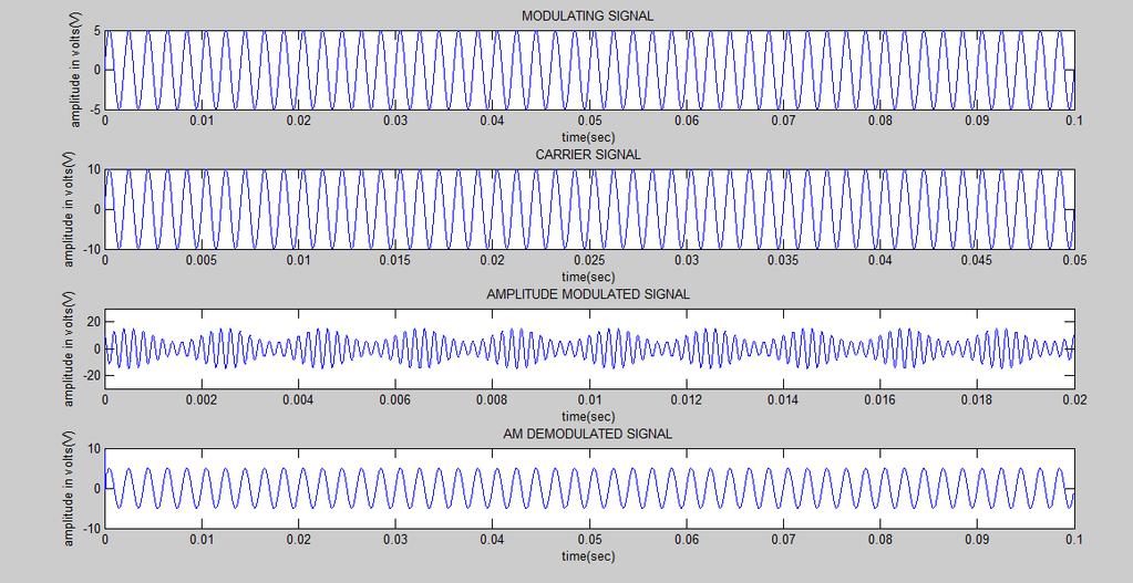
97 Output waveforms: 97
98 2. Frequency Modulation: clc clear all close all Fs = 8000; % Sampling rate of signal Fc = 100; % Carrier frequency t = linspace(0,1,10000); % Sampling times x = sin(2*pi*10*t) % Channel 1 dev = 75; % Frequency deviation in modulated signal y = fmmod(x,fc,fs,dev); % Modulate both channels. z = fmdemod(y,fc,fs,dev); % Demodulate both channels. subplot(411),plot(t,x) xlabel('time(sec)'); ylabel('amplitude in volts(v)'); title('modulating SIGNAL'); subplot(412),plot(t,sin(2*pi*fc*t)) xlabel('time(sec)'); ylabel('amplitude in volts(v)'); title('carrier SIGNAL'); subplot(413),plot(t,y) xlabel('time(sec)'); ylabel('amplitude in volts(v)'); title('frequency MODULATED SIGNAL'); subplot(414),plot(t,z) xlabel('time(sec)'); ylabel('amplitude in volts(v)'); title(' FM DEMODULATED SIGNAL'); 98
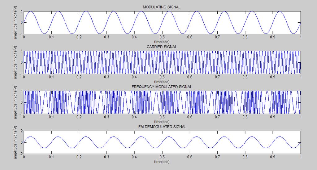
99 Output waveforms: 99
; n=length(s); for i=1:n if (m(i)>=s(i)) pwm(i)=0; elseif (m(i)<=s(i)) pwm(i)=1; end end Output waveforms: 100 subplot(211),plot(t,m,'-r',t,s,'-b');axis([0 2-1.5 1.")
100 3. Pulse Width Modulation: %PWM wave generation without functions clc; clear all; close all; t=0:0.001:2; s=sawtooth(2*pi*20*t+pi); m=0.75*sin(2*pi*1*t); n=length(s); for i=1:n if (m(i)>=s(i)) pwm(i)=0; elseif (m(i)<=s(i)) pwm(i)=1; end end Output waveforms: 100 subplot(211),plot(t,m,'-r',t,s,'-b');axis([ ]); title('message signal with sawtooth comparison') xlabel('time(sec)'); ylabel('voltage(v)'); subplot(212),plot(t,pwm,'-k') axis([ ]); title('pwm wave'); xlabel('time(sec)'); ylabel('voltage(v)');
101 4. Pulse Position Modulation: %PPM Modulation and Demodulation clc; clear all; close all; fc=4000; fs=40000; fm=1000; t=0:1/fs:(2/fm-1/fs); mt=0.4*sin(2*pi*fm*t)+0.5; st=modulate(mt,fc,fs,'ppm'); dt=demod(st,fc,fs,'ppm'); figure subplot(3,1,1); plot(mt); title('message signal'); xlabel('timeperiod'); ylabel('amplitude'); axis([ ]) subplot(3,1,2); plot(st); title(' PPM signal'); xlabel('timeperiod'); ylabel('amplitude'); axis([ ]) subplot(3,1,3); plot(dt); title(' PPM demodulated signal'); xlabel('timeperiod'); ylabel('amplitude');axis([ ]) 101

102 Output waveforms: 102
103 5. Pulse Amplitude Modulation: %Pulse Amplitude Modulation clc; clear all; close all; fc=100; fm=fc/10; fs=100*fc; t=0:1/fs:4/fm; mt=cos(2*pi*fm*t); ct=0.5*square(2*pi*fc*t)+0.5; st=mt.*ct; tt=[ ]; %single sided PAM for i=1:length(st); if st(i)==0; tt=[tt,st(i)]; else tt=[tt,st(i)+2]; end end figure(1) subplot(4,1,1); plot(t,mt); title('message signal'); xlabel('timeperiod'); ylabel('amplitude'); subplot(4,1,2); plot(t,ct); title('carrier signal'); xlabel('timeperiod'); ylabel('amplitude'); subplot(4,1,3); plot(t,st); title('bipolar PAM'); xlabel('timeperiod'); ylabel('amplitude'); subplot(4,1,4); plot(t,tt); title('pam'); xlabel('timeperiod'); ylabel('amplitude'); %demodulation dt=st.*ct; dt_frequency=fftshift(abs(fft(dt))); filter=fir1(200,fm/fs,'low'); original_t_signal=conv(filter,dt); original_f_signal=fftshift(abs(fft(original_t_signal))); t1=0:1/(length(original_t_signal)-1):1; f=-fs/2:fs/(length(original_f_signal)-1):fs/2; figure(2) subplot(2,1,1); plot(t1,original_t_signal); title('time domain signal'); xlabel('timeperiod'); ylabel('amplitude'); subplot(2,1,2); plot(f,original_f_signal); title('frequency domain signal'); xlabel('frequency'); ylabel('amplitude'); axis([ ]) 103

104 Output waveforms: Result: The generation and Detection of Analog Modulation schemes, Pulse Modulation schemes were observed using MATLAB. 104
105 Aim: 2.GENERATION & DETECTION OF PCM, DELTA MODULATION & DIGITAL MODULATION SCHEMES (ASK, FSK, BPSK, QPSK) BY USING MATLAB To Generate & to detect Modulation schemes like PCM, DM and Digital Modulation schemes like ASK, FSK, BPSK, and QPSK using MATLAB. Software required: MATLAB2010a Program: 1. ASK Modulation: %ASK Modulation clc; clear all; close all; %GENERATE CARRIER SIGNAL Tb=1; fc=10; t=0:tb/100:1; c=sqrt(2/tb)*sin(2*pi*fc*t); %generate message signal N=8; m=rand(1,n); t1=0;t2=tb for i=1:n t=[t1:.01:t2] if m(i)>0.5 m(i)=1; m_s=ones(1,length(t)); else m(i)=0; m_s=zeros(1,length(t)); 105
106 end message(i,:)=m_s; %product of carrier and message ask_sig(i,:)=c.*m_s; t1=t1+(tb+.01); t2=t2+(tb+.01); %plot the message and ASK signal subplot(5,1,2);axis([0 N -2 2]);plot(t,message(i,:),'r'); title('message signal');xlabel('t--->');ylabel('m(t)');grid on hold on subplot(5,1,4);plot(t,ask_sig(i,:)); title('ask signal');xlabel('t--->');ylabel('s(t)');grid on hold on end hold off %Plot the carrier signal and input binary data subplot(5,1,3);plot(t,c); title('carrier signal');xlabel('t--->');ylabel('c(t)');grid on subplot(5,1,1);stem(m); title('binary data bits');xlabel('n--->');ylabel('b(n)');grid on % ASK Demodulation t1=0;t2=tb for i=1:n t=[t1:tb/100:t2] %correlator x=sum(c.*ask_sig(i,:)); %decision device demod(i)=0; if x>0 demod(i)=1; else 106
; end %plot demodulated binary data bits subplot(5,1,5);stem(demod); title('ask demodulated signal');")
107 end t1=t1+(tb+.01); t2=t2+(tb+.01); end %plot demodulated binary data bits subplot(5,1,5);stem(demod); title('ask demodulated signal'); xlabel('n--->');ylabel('b(n)');grid on Output waveforms: 2. PSK Modulation: 107
108 % PSK modulation clc; clear all; close all; %GENERATE CARRIER SIGNAL Tb=1; t=0:tb/100:tb; fc=2; c=sqrt(2/tb)*sin(2*pi*fc*t); %generate message signal N=8; m=rand(1,n); t1=0;t2=tb for i=1:n t=[t1:.01:t2] if m(i)>0.5 m(i)=1; m_s=ones(1,length(t)); else m(i)=0; m_s=-1*ones(1,length(t)); end message(i,:)=m_s; %product of carrier and message signal bpsk_sig(i,:)=c.*m_s; %Plot the message and BPSK modulated signal subplot(5,1,2);axis([0 N -2 2]);plot(t,message(i,:),'r'); title('message signal(polar form)');xlabel('t--->');ylabel('m(t)'); grid on; hold on; subplot(5,1,4);plot(t,bpsk_sig(i,:)); title('bpsk signal');xlabel('t--->');ylabel('s(t)'); 108
109 grid on; hold on; t1=t1+1.01; t2=t2+1.01; end hold off %plot the input binary data and carrier signal subplot(5,1,1);stem(m); title('binary data bits');xlabel('n--->');ylabel('b(n)'); grid on; subplot(5,1,3);plot(t,c); title('carrier signal');xlabel('t--->');ylabel('c(t)');grid on; % PSK Demodulation t1=0;t2=tb for i=1:n t=[t1:.01:t2] %correlator x=sum(c.*bpsk_sig(i,:)); %decision device if x>0 demod(i)=1; else demod(i)=0; end t1=t1+1.01; t2=t2+1.01; end %plot the demodulated data bits subplot(5,1,5);stem(demod); title('demodulated data');xlabel('n--->');ylabel('b(n)'); grid on Output waveforms: 109

110 3. FSK Modulation: Modulation % FSK 110
111 clc; clear all; close all; %GENERATE CARRIER SIGNAL Tb=1; fc1=2;fc2=5; t=0:(tb/100):tb; c1=sqrt(2/tb)*sin(2*pi*fc1*t); c2=sqrt(2/tb)*sin(2*pi*fc2*t); %generate message signal N=10; m=rand(1,n); t1=0;t2=tb for i=1:n t=[t1:(tb/100):t2] if m(i)>0.5 m(i)=1; m_s=ones(1,length(t)); invm_s=zeros(1,length(t)); else m(i)=0; m_s=zeros(1,length(t)); invm_s=ones(1,length(t)); end message(i,:)=m_s; %Multiplier fsk_sig1(i,:)=c1.*m_s; fsk_sig2(i,:)=c2.*invm_s; fsk=fsk_sig1+fsk_sig2; %plotting the message signal and the modulated signal subplot(3,2,2);axis([0 N -2 2]);plot(t,message(i,:),'r'); title('message signal');xlabel('t---->');ylabel('m(t)');grid on;hold on; 111
112 subplot(3,2,5);plot(t,fsk(i,:)); title('fsk signal');xlabel('t---->');ylabel('s(t)');grid on;hold on; t1=t1+(tb+.01); t2=t2+(tb+.01); end hold off %Plotting binary data bits and carrier signal subplot(3,2,1);stem(m); title('binary data');xlabel('n---->'); ylabel('b(n)');grid on; subplot(3,2,3);plot(t,c1); title('carrier signal-1');xlabel('t---->');ylabel('c1(t)');grid on; subplot(3,2,4);plot(t,c2); title('carrier signal-2');xlabel('t---->');ylabel('c2(t)');grid on; 13 % FSK Demodulation t1=0;t2=tb for i=1:n t=[t1:(tb/100):t2] %correlator x1=sum(c1.*fsk_sig1(i,:)); x2=sum(c2.*fsk_sig2(i,:)); x=x1-x2; %decision device if x>0 demod(i)=1; else demod(i)=0; end t1=t1+(tb+.01); t2=t2+(tb+.01); end %Plotting the demodulated data bits 112
;xlabel('n---->');ylabel('b(n)'); grid on; Output waveforms: 4.")
113 subplot(3,2,6);stem(demod); title(' demodulated data');xlabel('n---->');ylabel('b(n)'); grid on; Output waveforms: 4. QPSK Modulation: % QPSK Modulation clc; 113
114 clear all; close all; %GENERATE QUADRATURE CARRIER SIGNAL Tb=1;t=0:(Tb/100):Tb;fc=1; c1=sqrt(2/tb)*cos(2*pi*fc*t); c2=sqrt(2/tb)*sin(2*pi*fc*t); %generate message signal N=16;m=rand(1,N); t1=0;t2=tb for i=1:2:(n-1) t=[t1:(tb/100):t2] if m(i)>0.5 m(i)=1; m_s=ones(1,length(t)); else m(i)=0; m_s=-1*ones(1,length(t)); end %odd bits modulated signal odd_sig(i,:)=c1.*m_s; if m(i+1)> m(i+1)=1; m_s=ones(1,length(t)); else m(i+1)=0; m_s=-1*ones(1,length(t)); end %even bits modulated signal even_sig(i,:)=c2.*m_s; %qpsk signal 114
115 qpsk=odd_sig+even_sig; %Plot the QPSK modulated signal subplot(3,2,4);plot(t,qpsk(i,:)); title('qpsk signal');xlabel('t---->');ylabel('s(t)');grid on; hold on; t1=t1+(tb+.01); t2=t2+(tb+.01); end hold off %Plot the binary data bits and carrier signal subplot(3,2,1);stem(m); title('binary data bits');xlabel('n---->');ylabel('b(n)');grid on; subplot(3,2,2);plot(t,c1); title('carrier signal-1');xlabel('t---->');ylabel('c1(t)');grid on; subplot(3,2,3);plot(t,c2); title('carrier signal-2');xlabel('t---->');ylabel('c2(t)');grid on; % QPSK Demodulation t1=0;t2=tb for i=1:n-1 t=[t1:(tb/100):t2] %correlator x1=sum(c1.*qpsk(i,:)); x2=sum(c2.*qpsk(i,:)); %decision device if (x1>0&&x2>0) demod(i)=1; demod(i+1)=1; elseif (x1>0&&x2<0) demod(i)=1; demod(i+1)=0; demod(i+1)=0; elseif (x1<0&&x2<0) demod(i)=0; 115
116 elseif (x1<0&&x2>0) demod(i)=0; demod(i+1)=1; end t1=t1+(tb+.01); t2=t2+(tb+.01); end subplot(3,2,5);stem(demod); title('qpsk demodulated bits');xlabel('n---->');ylabel('b(n)');grid on; Output waveforms: 116

117 5. Pulse Code Modulation: clc; clear all; 117
118 t = 0:0.005:20; partition = -1:0.2:2; codebook = -1:0.2:2.2; x = sin(t); [index,quants] = quantiz(x,partition,codebook); subplot(3,1,1); plot(t,x); title('message Signal'); xlabel('time(s) ---->') ylabel('amplitude(v) ---->') subplot(3,1,2); plot(t,quants); title('quantized Signal'); xlabel('time(s) ---->') ylabel('amplitude(v) ---->') y = uencode(quants,3); subplot(3,1,3); plot(t,y); title('pcm Signal'); xlabel('time(s) ---->'); ylabel('amplitude(v) ---->') Output waveforms: 118

119 5. Delta Modulation: t=[0:0.01:1] %t is the time we are considering for our calculation. Even signal time period is 1 second 119
120 m=sinc(2*pi*t) %genrates the sinc pulse with the time period of t subplot(211) %opens the figure window and splits it into two parts horizontally hold on %all the graphs drawn after this command will be plotted on the first part of the figure plot(m,'*black') %plotting the sinc pulse with the *'s title('sinc pulse') %putting the title for the graph drawn earlier xlabel('time')%specifies the xlabel for our graph ylabel('amplitude')%specifies the ylabel for our figure d=2*pi/100 %d is the step size we are dividing the total time period into 100 parts of same size %Logic to calculate the delta modulation signal %We have total 100 samples over the time period of t %When the delta modulation we consider error signal is same as the sampled version of the incoming signal %and we will quantize the error signal %mq is the star case approximates signal and is is equal to the previous time frame step approximation plus the quantized error signal for the current sample for n=1:1:100 end if n==1 else end e(n)=m(n) eq(n)=d*sign(e(n)) mq(n)=eq(n) e(n)=m(n)-mq(n-1) eq(n)=d*sign(e(n)) mq(n)=mq(n-1)+eq(n) %draw the quantized version of the signal on the graph of original signal stairs(mq,'red') hleg=legend('original signal','stair case approximated signal') 120
121 hold off %Deltma Modulation of Sine wave subplot(212) hold on m1=sin(2*pi*t) plot(m1,'red') title('sin wave') xlabel('time') ylabel('amplitude') d=2*pi/100 for n=1:1:100 if n==1 e1(n)=m1(n) eq1(n)=d*sign(e1(n)) mq1(n)=eq1(n) else e1(n)=m1(n)-mq1(n-1) end end eq1(n)=d*sign(e1(n)) mq1(n)=mq1(n-1)+eq1(n) stairs(mq1,'blue') hleg=legend('original signal','stair case approximated signal') hold off Output waveforms: 121

122 Result: To Generation and Detection of Modulation schemes like PCM, DM and Digital Modulation schemes like ASK, FSK, BPSK, and QPSK using MATLAB. 122
Communication Systems Lab
 LAB MANUAL Communication Systems Lab (EE-226-F) Prepared by: Varun Sharma (Lab In-charge) Dayal C. Sati (Faculty In-charge) B R C M CET BAHAL DEPARTMENT OF ELECTRONICS & COMMUNICATION ENGINEERING Page
DIGITAL COMMUNICATIONS LAB
 DIGITAL COMMUNICATIONS LAB List of Experiments: 1. PCM Generation and Detection. 2. Differential Pulse Code modulation. 3. Delta modulation. 4. Time Division Multiplexing of 2band Limited Signals. 5. Frequency
DEPARTMENT OF E.C.E.
 PVP SIDDHARTHA INSTITUTE OF TECHNOLOGY, KANURU, VIJAYAWADA-7 DEPARTMENT OF E.C.E. ANALOG COMMUNICATIONS LAB MANUAL Department of Electronics & Communication engineering Prasad V.Potluri Siddhartha Institute
1 Analog and Digital Communication Lab
 1 2 Amplitude modulator trainer kit diagram AM Detector trainer kit Diagram 3 4 Calculations: 5 Result: 6 7 8 Balanced modulator circuit diagram Generation of DSB-SC 1. For the same circuit apply the modulating
Amplitude modulator trainer kit diagram
 Amplitude modulator trainer kit diagram AM Detector trainer kit Diagram Calculations: Result: Pre lab test (20) Observation (20) Simulation (20) Remarks & Signature with Date Circuit connection (30) Result
Department of Electronics & Telecommunication Engg. LAB MANUAL. B.Tech V Semester [ ] (Branch: ETE)
![Department of Electronics & Telecommunication Engg. LAB MANUAL. B.Tech V Semester [ ] (Branch: ETE)](/thumbs/86/93078052.jpg "Department of Electronics & Telecommunication Engg. LAB MANUAL. B.Tech V Semester [ ] (Branch: ETE)") Department of Electronics & Telecommunication Engg. LAB MANUAL SUBJECT:-DIGITAL COMMUNICATION SYSTEM [BTEC-501] B.Tech V Semester [2013-14] (Branch: ETE) KCT COLLEGE OF ENGG & TECH., FATEHGARH PUNJAB TECHNICAL
Department of Electronics & Telecommunication Engg. LAB MANUAL SUBJECT:-DIGITAL COMMUNICATION SYSTEM [BTEC-501] B.Tech V Semester [2013-14] (Branch: ETE) KCT COLLEGE OF ENGG & TECH., FATEHGARH PUNJAB TECHNICAL
AC LAB ECE-D ecestudy.wordpress.com
 PART B EXPERIMENT NO: 1 AIM: PULSE AMPLITUDE MODULATION (PAM) & DEMODULATION DATE: To study Pulse Amplitude modulation and demodulation process with relevant waveforms. APPARATUS: 1. Pulse amplitude modulation
EXPERIMENT WISE VIVA QUESTIONS
 EXPERIMENT WISE VIVA QUESTIONS Pulse Code Modulation: 1. Draw the block diagram of basic digital communication system. How it is different from analog communication system. 2. What are the advantages of
LABORATORY EXPERIMENTS DIGITAL COMMUNICATION
 LABORATORY EXPERIMENTS DIGITAL COMMUNICATION INDEX S. No. Name of the Program 1 Study of Pulse Amplitude Modulation (PAM) and Demodulation. 2 Study of Pulse Width Modulation (PWM) and Demodulation. 3 Study
AM, PM and FM mo m dula l ti t o i n
 AM, PM and FM modulation What is amplitude modulation In order that a radio signal can carry audio or other information for broadcasting or for two way radio communication, it must be modulated or changed
Department of Electronics & Communication Engineering LAB MANUAL SUBJECT: DIGITAL COMMUNICATION LABORATORY [ECE324] (Branch: ECE)
![Department of Electronics & Communication Engineering LAB MANUAL SUBJECT: DIGITAL COMMUNICATION LABORATORY [ECE324] (Branch: ECE)](/thumbs/96/127341232.jpg "Department of Electronics & Communication Engineering LAB MANUAL SUBJECT: DIGITAL COMMUNICATION LABORATORY [ECE324] (Branch: ECE)") Department of Electronics & Communication Engineering LAB MANUAL SUBJECT: DIGITAL COMMUNICATION LABORATORY [ECE324] B.Tech Year 3 rd, Semester - 5 th (Branch: ECE) Version: 01 st August 2018 The LNM Institute
Department of Electronics & Communication Engineering LAB MANUAL SUBJECT: DIGITAL COMMUNICATION LABORATORY [ECE324] B.Tech Year 3 rd, Semester - 5 th (Branch: ECE) Version: 01 st August 2018 The LNM Institute
Amplitude Modulated Systems
 Amplitude Modulated Systems Communication is process of establishing connection between two points for information exchange. Channel refers to medium through which message travels e.g. wires, links, or
Data Conversion Circuits & Modulation Techniques. Subhasish Chandra Assistant Professor Department of Physics Institute of Forensic Science, Nagpur
 Data Conversion Circuits & Modulation Techniques Subhasish Chandra Assistant Professor Department of Physics Institute of Forensic Science, Nagpur Data Conversion Circuits 2 Digital systems are being used
Let us consider the following block diagram of a feedback amplifier with input voltage feedback fraction,, be positive i.e. in phase.
 P a g e 2 Contents 1) Oscillators 3 Sinusoidal Oscillators Phase Shift Oscillators 4 Wien Bridge Oscillators 4 Square Wave Generator 5 Triangular Wave Generator Using Square Wave Generator 6 Using Comparator
B.Tech II Year II Semester (R13) Supplementary Examinations May/June 2017 ANALOG COMMUNICATION SYSTEMS (Electronics and Communication Engineering)
 Supplementary Examinations May/June 2017 ANALOG COMMUNICATION SYSTEMS (Electronics and Communication Engineering)") Code: 13A04404 R13 B.Tech II Year II Semester (R13) Supplementary Examinations May/June 2017 ANALOG COMMUNICATION SYSTEMS (Electronics and Communication Engineering) Time: 3 hours Max. Marks: 70 PART A
Code: 13A04404 R13 B.Tech II Year II Semester (R13) Supplementary Examinations May/June 2017 ANALOG COMMUNICATION SYSTEMS (Electronics and Communication Engineering) Time: 3 hours Max. Marks: 70 PART A
CHAPTER 2. Instructor: Mr. Abhijit Parmar Course: Mobile Computing and Wireless Communication ( )
") CHAPTER 2 Instructor: Mr. Abhijit Parmar Course: Mobile Computing and Wireless Communication (2170710) Syllabus Chapter-2.3 Modulation Techniques Reasons for Choosing Encoding Techniques Digital data,
CHAPTER 2 Instructor: Mr. Abhijit Parmar Course: Mobile Computing and Wireless Communication (2170710) Syllabus Chapter-2.3 Modulation Techniques Reasons for Choosing Encoding Techniques Digital data,
GOVERNMENT OF KARNATAKA KARNATAKA STATE PRE-UNIVERSITY EDUCATION EXAMINATION BOARD II YEAR PUC EXAMINATION MARCH-2013 SCHEME OF VALUATION
 GOVERNMENT OF KARNATAKA KARNATAKA STATE PRE-UNIVERSITY EDUCATION EXAMINATION BOARD II YEAR PUC EXAMINATION MARCH-03 SCHEME OF VALUATION Subject Code: 0 Subject: PART - A 0. What does the arrow mark indicate
Jawaharlal Nehru Engineering College
 Jawaharlal Nehru Engineering College Laboratory Manual COMMUNICATION ENGINEERING For Author JNEC, Aurangabad. Second Year Students Lab manual made by PROF. S.A. ANNANDATE PROF. P. B. MURMUDE PROF. P.B.YADAV
BINARY AMPLITUDE SHIFT KEYING
 BINARY AMPLITUDE SHIFT KEYING AIM: To set up a circuit to generate Binary Amplitude Shift keying and to plot the output waveforms. COMPONENTS AND EQUIPMENTS REQUIRED: IC CD4016, IC 7474, Resistors, Zener
Modulation is the process of impressing a low-frequency information signal (baseband signal) onto a higher frequency carrier signal
 onto a higher frequency carrier signal") Modulation is the process of impressing a low-frequency information signal (baseband signal) onto a higher frequency carrier signal Modulation is a process of mixing a signal with a sinusoid to produce
Modulation is the process of impressing a low-frequency information signal (baseband signal) onto a higher frequency carrier signal Modulation is a process of mixing a signal with a sinusoid to produce
CSCD 433 Network Programming Fall Lecture 5 Physical Layer Continued
 CSCD 433 Network Programming Fall 2016 Lecture 5 Physical Layer Continued 1 Topics Definitions Analog Transmission of Digital Data Digital Transmission of Analog Data Multiplexing 2 Different Types of
Engr M. Hadi Ali Khan B. Sc. Engg (AMU), MIETE (India), Ex-MIEEE (USA), Ex-MSSI (India)
, MIETE (India), Ex-MIEEE (USA), Ex-MSSI (India)") Page 1 of 26 Department of Electronics Engineering, Communication Systems Laboratory Laboratory Manual for B. Tech. (Electronics), III Year (VI Semester) Lab Course EL 394 ( Communication Lab. II) List
Page 1 of 26 Department of Electronics Engineering, Communication Systems Laboratory Laboratory Manual for B. Tech. (Electronics), III Year (VI Semester) Lab Course EL 394 ( Communication Lab. II) List
CSCD 433 Network Programming Fall Lecture 5 Physical Layer Continued
 CSCD 433 Network Programming Fall 2016 Lecture 5 Physical Layer Continued 1 Topics Definitions Analog Transmission of Digital Data Digital Transmission of Analog Data Multiplexing 2 Different Types of
DIGITAL COMMUNICATION
 DIGITAL COMMUNICATION TRAINING LAB Digital communication has emerged to augment or replace the conventional analog systems, which had been used widely a few decades back. Digital communication has demonstrated
GOVERNMENT OF KARNATAKA KARNATAKA STATE PRE-UNIVERSITY EDUCATION EXAMINATION BOARD II YEAR PUC EXAMINATION MARCH-2012 SCHEME OF VALUATION
 GOVERNMENT OF KARNATAKA KARNATAKA STATE PRE-UNIVERSITY EDUCATION EXAMINATION BOARD II YEAR PUC EXAMINATION MARCH-0 SCHEME OF VALUATION Subject Code: 0 Subject: Qn. PART - A 0. Which is the largest of three
Communications I (ELCN 306)
") Communications I (ELCN 306) c Samy S. Soliman Electronics and Electrical Communications Engineering Department Cairo University, Egypt Email: samy.soliman@cu.edu.eg Website: http://scholar.cu.edu.eg/samysoliman
Communications I (ELCN 306) c Samy S. Soliman Electronics and Electrical Communications Engineering Department Cairo University, Egypt Email: samy.soliman@cu.edu.eg Website: http://scholar.cu.edu.eg/samysoliman
Time division multiplexing The block diagram for TDM is illustrated as shown in the figure
 CHAPTER 2 Syllabus: 1) Pulse amplitude modulation 2) TDM 3) Wave form coding techniques 4) PCM 5) Quantization noise and SNR 6) Robust quantization Pulse amplitude modulation In pulse amplitude modulation,
Signal Encoding Techniques
 2 Techniques ITS323: to Data Communications CSS331: Fundamentals of Data Communications Sirindhorn International Institute of Technology Thammasat University Prepared by Steven Gordon on 3 August 2015
SEN366 Computer Networks
 SEN366 Computer Networks Prof. Dr. Hasan Hüseyin BALIK (5 th Week) 5. Signal Encoding Techniques 5.Outline An overview of the basic methods of encoding digital data into a digital signal An overview of
The steeper the phase shift as a function of frequency φ(ω) the more stable the frequency of oscillation
 the more stable the frequency of oscillation") It should be noted that the frequency of oscillation ω o is determined by the phase characteristics of the feedback loop. the loop oscillates at the frequency for which the phase is zero The steeper the
It should be noted that the frequency of oscillation ω o is determined by the phase characteristics of the feedback loop. the loop oscillates at the frequency for which the phase is zero The steeper the
Data Encoding g(p (part 2)
") Data Encoding g(p (part 2) CSE 3213 Instructor: U.T. Nguyen 10/11/2007 12:44 PM 1 Analog Data, Digital Signals (5.3) 2 1 Analog Data, Digital Signals Digitization Conversion of analog data into digital
Data Encoding g(p (part 2) CSE 3213 Instructor: U.T. Nguyen 10/11/2007 12:44 PM 1 Analog Data, Digital Signals (5.3) 2 1 Analog Data, Digital Signals Digitization Conversion of analog data into digital
Dhanalakshmi College of Engineering Manimangalam, Tambaram, Chennai
 Dhanalakshmi College of Engineering Manimangalam, Tambaram, Chennai 601 301 DEPARTMENT OF ELECTRONICS AND COMMUNICATION ENGINEERING V SEMESTER - R 2013 EC6512 COMMUNICATION SYSTEMS LABORATORY LABORATORY
GOVERNMENT OF KARNATAKA KARNATAKA STATE PRE-UNIVERSITY EDUCATION EXAMINATION BOARD II YEAR PUC EXAMINATION JULY-2012 SCHEME OF VALUATION
 GOVERNMENT OF KARNATAKA KARNATAKA STATE PRE-UNIVERSITY EDUCATION EXAMINATION BOARD II YEAR PUC EXAMINATION JULY-0 SCHEME OF VALUATION Subject Code: 40 Subject: PART - A 0. Which region of the transistor
ELEC3242 Communications Engineering Laboratory Amplitude Modulation (AM)
") ELEC3242 Communications Engineering Laboratory 1 ---- Amplitude Modulation (AM) 1. Objectives 1.1 Through this the laboratory experiment, you will investigate demodulation of an amplitude modulated (AM)
ELEC3242 Communications Engineering Laboratory 1 ---- Amplitude Modulation (AM) 1. Objectives 1.1 Through this the laboratory experiment, you will investigate demodulation of an amplitude modulated (AM)
CHETTINAD COLLEGE OF ENGINEERING & TECHNOLOGY NH-67, TRICHY MAIN ROAD, PULIYUR, C.F , KARUR DT.
 CHETTINAD COLLEGE OF ENGINEERING & TECHNOLOGY NH-67, TRICHY MAIN ROAD, PULIYUR, C.F. 639 114, KARUR DT. DEPARTMENT OF ELECTRONICS AND COMMUNICATION ENGINEERING COURSE MATERIAL Subject Name: Analog & Digital
Electronic & Telecommunication Engineering
 Department of Electronic & Telecommunication Engineering LAB MANUAL Analog Communication System B.Tech IV Semester KCT College OF ENGG AND TECH. VILLAGE FATEHGARH DISTT.SANGRUR INDEX Sr.No: Experiments
Operating Manual Ver 1.1
 Frequency Modulation and Demodulation Trainer ST2203 Operating Manual Ver 1.1 An ISO 9001 : 2000 company 94-101, Electronic Complex Pardesipura, Indore- 452010, India Tel : 91-731- 2570301/02, 4211100
BAPATLA ENGINEERING COLLEGE DIGITAL COMMUNICATIONS LAB EC-451. PREPARED BY S. Pallaviram, Lecturer
 BAPATLA ENGINEERING COLLEGE DIGITAL COMMUNICATIONS LAB EC-451 PREPARED BY S. Pallaviram, Lecturer Department of Electronics and Communications Engineering Bapatla Engineering College (Affiliated to Acharya
RAO PAHALD SINGH GROUP OF INSTITUTIONS BALANA(MOHINDER GARH)123029
123029") 1 COMMUNICATION SYSTEM LAB (EE-226 -F) Communication System Lab (EE-226-F) LAB MANUAL IV SEMESTER RAO PAHALD SINGH GROUP OF INSTITUTIONS BALANA(MOHINDER GARH)123029 Department Of Electronics and Communication
1 COMMUNICATION SYSTEM LAB (EE-226 -F) Communication System Lab (EE-226-F) LAB MANUAL IV SEMESTER RAO PAHALD SINGH GROUP OF INSTITUTIONS BALANA(MOHINDER GARH)123029 Department Of Electronics and Communication
Pulse Code Modulation
 Pulse Code Modulation Modulation is the process of varying one or more parameters of a carrier signal in accordance with the instantaneous values of the message signal. The message signal is the signal
Emona Telecoms-Trainer ETT-101
 EXPERIMENTS IN MODERN COMMUNICATIONS Emona Telecoms-Trainer ETT-101 Multi-Experiment Single Board Telecommunications Trainer for Technical College and Technical High School Students EMONA INSTRUMENTS www.ett101.com
UNIT-2 Angle Modulation System
 UNIT-2 Angle Modulation System Introduction There are three parameters of a carrier that may carry information: Amplitude Frequency Phase Frequency Modulation Power in an FM signal does not vary with modulation
Downloaded from 1
 VII SEMESTER FINAL EXAMINATION-2004 Attempt ALL questions. Q. [1] How does Digital communication System differ from Analog systems? Draw functional block diagram of DCS and explain the significance of
EXPERIMENT 2: Frequency Shift Keying (FSK)
") EXPERIMENT 2: Frequency Shift Keying (FSK) 1) OBJECTIVE Generation and demodulation of a frequency shift keyed (FSK) signal 2) PRELIMINARY DISCUSSION In FSK, the frequency of a carrier signal is modified
EXPERIMENT 2: Frequency Shift Keying (FSK) 1) OBJECTIVE Generation and demodulation of a frequency shift keyed (FSK) signal 2) PRELIMINARY DISCUSSION In FSK, the frequency of a carrier signal is modified
EE 400L Communications. Laboratory Exercise #7 Digital Modulation
 EE 400L Communications Laboratory Exercise #7 Digital Modulation Department of Electrical and Computer Engineering University of Nevada, at Las Vegas PREPARATION 1- ASK Amplitude shift keying - ASK - in
Lecture 6. Angle Modulation and Demodulation
 Lecture 6 and Demodulation Agenda Introduction to and Demodulation Frequency and Phase Modulation Angle Demodulation FM Applications Introduction The other two parameters (frequency and phase) of the carrier
CHAPTER 2 DIGITAL MODULATION
 2.1 INTRODUCTION CHAPTER 2 DIGITAL MODULATION Referring to Equation (2.1), if the information signal is digital and the amplitude (lv of the carrier is varied proportional to the information signal, a
ELEC3242 Communications Engineering Laboratory Frequency Shift Keying (FSK)
") ELEC3242 Communications Engineering Laboratory 1 ---- Frequency Shift Keying (FSK) 1) Frequency Shift Keying Objectives To appreciate the principle of frequency shift keying and its relationship to analogue
ELEC3242 Communications Engineering Laboratory 1 ---- Frequency Shift Keying (FSK) 1) Frequency Shift Keying Objectives To appreciate the principle of frequency shift keying and its relationship to analogue
College of information Technology Department of Information Networks Telecommunication & Networking I Chapter 5. Analog Transmission
 Analog Transmission 5.1 DIGITAL-TO-ANALOG CONVERSION Digital-to-analog conversion is the process of changing one of the characteristics of an analog signal based on the information in digital data. The
Digital Communication
 Digital Communication Laboratories bako@ieee.org DigiCom Labs There are 5 labs related to the digital communication. Study of the parameters of metal cables including: characteristic impendance, attenuation
 DEPARTMENT OF COMPUTER GCE@Bodi_ SCIENCE GCE@Bodi_ AND ENIGNEERING GCE@Bodi_ GCE@Bodi_ GCE@Bodi_ Analog and Digital Communication GCE@Bodi_ DEPARTMENT OF CsE Subject Name: Analog and Digital Communication
Speech, music, images, and video are examples of analog signals. Each of these signals is characterized by its bandwidth, dynamic range, and the
 Speech, music, images, and video are examples of analog signals. Each of these signals is characterized by its bandwidth, dynamic range, and the nature of the signal. For instance, in the case of audio
Dev Bhoomi Institute Of Technology Department of Electronics and Communication Engineering PRACTICAL INSTRUCTION SHEET REV. NO. : REV.
 Dev Bhoomi Institute Of Technology Department of Electronics and Communication Engineering PRACTICAL INSTRUCTION SHEET LABORATORY MANUAL EXPERIMENT NO. ISSUE NO. : ISSUE DATE: July 200 REV. NO. : REV.
SIR PADAMPAT SINGHANIA UNIVERSITY UDAIPUR Sample Question Paper for Ph.D. (Electronics & Communication Engineering) SPSAT 18
 SPSAT 18") INSTRUCTIONS SIR PADAMPAT SINGHANIA UNIVERSITY UDAIPUR Sample Question Paper for Ph.D. (Electronics & Communication Engineering) SPSAT 18 The test is 60 minutes long and consists of 40 multiple choice
INSTRUCTIONS SIR PADAMPAT SINGHANIA UNIVERSITY UDAIPUR Sample Question Paper for Ph.D. (Electronics & Communication Engineering) SPSAT 18 The test is 60 minutes long and consists of 40 multiple choice
Experiment # (3) PCM Modulator
 PCM Modulator") Islamic University of Gaza Faculty of Engineering Electrical Department Experiment # (3) PCM Modulator Digital Communications Lab. Prepared by: Eng. Mohammed K. Abu Foul Experiment Objectives: 1. To understand
Islamic University of Gaza Faculty of Engineering Electrical Department Experiment # (3) PCM Modulator Digital Communications Lab. Prepared by: Eng. Mohammed K. Abu Foul Experiment Objectives: 1. To understand
cosω t Y AD 532 Analog Multiplier Board EE18.xx Fig. 1 Amplitude modulation of a sine wave message signal
 University of Saskatchewan EE 9 Electrical Engineering Laboratory III Amplitude and Frequency Modulation Objectives: To observe the time domain waveforms and spectra of amplitude modulated (AM) waveforms
CATALOG. ANALOG COMMUNICATION SYSTEMS DIGITAL COMMUNICATION SYSTEMS Microcontroller kits Arm controller kits PLC Trainer KITS Regulated Power supplies
 CATALOG ANALOG COMMUNICATION SYSTEMS DIGITAL COMMUNICATION SYSTEMS Microcontroller kits Arm controller kits PLC Trainer KITS Regulated Power supplies UNION INTRUMENTS #17 & 18, 4 th floor, Hanumathra Arcade
CHAPTER 4. PULSE MODULATION Part 2
 CHAPTER 4 PULSE MODULATION Part 2 Pulse Modulation Analog pulse modulation: Sampling, i.e., information is transmitted only at discrete time instants. e.g. PAM, PPM and PDM Digital pulse modulation: Sampling
Chapter-1: Introduction
 Chapter-1: Introduction The purpose of a Communication System is to transport an information bearing signal from a source to a user destination via a communication channel. MODEL OF A COMMUNICATION SYSTEM
B.E. SEMESTER III (ELECTRICAL) SUBJECT CODE: X30902 Subject Name: Analog & Digital Electronics
 SUBJECT CODE: X30902 Subject Name: Analog & Digital Electronics") B.E. SEMESTER III (ELECTRICAL) SUBJECT CODE: X30902 Subject Name: Analog & Digital Electronics Sr. No. Date TITLE To From Marks Sign 1 To verify the application of op-amp as an Inverting Amplifier 2 To
B.E. SEMESTER III (ELECTRICAL) SUBJECT CODE: X30902 Subject Name: Analog & Digital Electronics Sr. No. Date TITLE To From Marks Sign 1 To verify the application of op-amp as an Inverting Amplifier 2 To
EE 460L University of Nevada, Las Vegas ECE Department
 EE 460L PREPARATION 1- ASK Amplitude shift keying - ASK - in the context of digital communications is a modulation process which imparts to a sinusoid two or more discrete amplitude levels. These are related
TE 302 DISCRETE SIGNALS AND SYSTEMS. Chapter 1: INTRODUCTION
 TE 302 DISCRETE SIGNALS AND SYSTEMS Study on the behavior and processing of information bearing functions as they are currently used in human communication and the systems involved. Chapter 1: INTRODUCTION
LINEAR IC APPLICATIONS
 1 B.Tech III Year I Semester (R09) Regular & Supplementary Examinations December/January 2013/14 1 (a) Why is R e in an emitter-coupled differential amplifier replaced by a constant current source? (b)
Pulse-Width Modulation (PWM)
") Pulse-Width Modulation (PWM) Modules: Integrate & Dump, Digital Utilities, Wideband True RMS Meter, Tuneable LPF, Audio Oscillator, Multiplier, Utilities, Noise Generator, Speech, Headphones. 0 Pre-Laboratory
Pulse-Width Modulation (PWM) Modules: Integrate & Dump, Digital Utilities, Wideband True RMS Meter, Tuneable LPF, Audio Oscillator, Multiplier, Utilities, Noise Generator, Speech, Headphones. 0 Pre-Laboratory
Analog and Telecommunication Electronics
 Politecnico di Torino Electronic Eng. Master Degree Analog and Telecommunication Electronics C5 - Synchronous demodulation» AM and FM demodulation» Coherent demodulation» Tone decoders AY 2015-16 19/03/2016-1
Class 4 ((Communication and Computer Networks))
)") Class 4 ((Communication and Computer Networks)) Lesson 5... SIGNAL ENCODING TECHNIQUES Abstract Both analog and digital information can be encoded as either analog or digital signals. The particular encoding
Class 4 ((Communication and Computer Networks)) Lesson 5... SIGNAL ENCODING TECHNIQUES Abstract Both analog and digital information can be encoded as either analog or digital signals. The particular encoding
UNIT TEST I Digital Communication
 Time: 1 Hour Class: T.E. I & II Max. Marks: 30 Q.1) (a) A compact disc (CD) records audio signals digitally by using PCM. Assume the audio signal B.W. to be 15 khz. (I) Find Nyquist rate. (II) If the Nyquist
Learning Material Ver 1.1
 Data Formatting & Carrier Modulation Transmitter Trainer and Carrier Demodulation & Data Reformatting Receiver Trainer ST2106 & ST2107 Learning Material Ver 1.1 An ISO 9001 : 2000 company 94, Electronic
FDM- FREQUENCY DIVISION MULTIPLEXING
 FDM- FREQUENCY DIVISION MULTIPLEXING Multiplexing to refer to the combination of information streams from multiple sources for transmission over a shared medium Demultiplexing to refer to the separation
ANALOG COMMUNICATION
 ANALOG COMMUNICATION TRAINING LAB Analog Communication Training Lab consists of six kits, one each for Modulation (ACL-01), Demodulation (ACL-02), Modulation (ACL-03), Demodulation (ACL-04), Noise power
YEDITEPE UNIVERSITY ENGINEERING FACULTY COMMUNICATION SYSTEMS LABORATORY EE 354 COMMUNICATION SYSTEMS
 YEDITEPE UNIVERSITY ENGINEERING FACULTY COMMUNICATION SYSTEMS LABORATORY EE 354 COMMUNICATION SYSTEMS EXPERIMENT 3: SAMPLING & TIME DIVISION MULTIPLEX (TDM) Objective: Experimental verification of the
TE 0224 ANALOG COMMUNICATION LAB. Laboratory Manual
 TE 0224 ANALOG COMMUNICATION LAB Laboratory Manual DEPARTMENT OF TELECOMMUNICATION ENGINEERING SRM UNIVERSITY S.R.M. NAGAR, KATTANKULATHUR 603 203. FOR PRIVATE CIRCULATION ONLY ALL RIGHTS RESERVED DEPARTMENT
Elements of Communication System Channel Fig: 1: Block Diagram of Communication System Terminology in Communication System
 Content:- Fundamentals of Communication Engineering : Elements of a Communication System, Need of modulation, electromagnetic spectrum and typical applications, Unit V (Communication terminologies in communication
EE-4022 Experiment 2 Amplitude Modulation (AM)
") EE-4022 MILWAUKEE SCHOOL OF ENGINEERING 2015 Page 2-1 Student objectives: EE-4022 Experiment 2 Amplitude Modulation (AM) In this experiment the student will use laboratory modules to implement operations
EE-4022 MILWAUKEE SCHOOL OF ENGINEERING 2015 Page 2-1 Student objectives: EE-4022 Experiment 2 Amplitude Modulation (AM) In this experiment the student will use laboratory modules to implement operations
EEE 309 Communication Theory
 EEE 309 Communication Theory Semester: January 2017 Dr. Md. Farhad Hossain Associate Professor Department of EEE, BUET Email: mfarhadhossain@eee.buet.ac.bd Office: ECE 331, ECE Building Types of Modulation
SEM: V EXAM MARKS: 50 BRANCH: EC IA MARKS: 25 SUBJECT: ANALOG COMMUNICATION & LIC LAB SUB CODE: 06ECL58
 LIST OF EXPERIMENTS SEM: V EXAM MARKS: 50 BRANCH: EC IA MARKS: 25 SUBJECT: ANALOG COMMUNICATION & LIC LAB SUB CODE: 06ECL58 1) Active low pass & high pass filters second order 2) Active band pass & band
ADVANCED EXPERIMENTS IN MODERN COMMUNICATIONS
 ADVANCED EXPERIMENTS IN MODERN COMMUNICATIONS NEW FIBER OPTICS KIT New Generation Single-Board Telecoms Experimenter for Advanced Experiments Emona ETT-101 BiSKIT Multi-Experiment Telecommunications &
Experiment 7: Frequency Modulation and Phase Locked Loops
 Experiment 7: Frequency Modulation and Phase Locked Loops Frequency Modulation Background Normally, we consider a voltage wave form with a fixed frequency of the form v(t) = V sin( ct + ), (1) where c
Universitas Sumatera Utara
 Amplitude Shift Keying & Frequency Shift Keying Aim: To generate and demodulate an amplitude shift keyed (ASK) signal and a binary FSK signal. Intro to Generation of ASK Amplitude shift keying - ASK -
CS441 Mobile & Wireless Computing Communication Basics
 Department of Computer Science Southern Illinois University Carbondale CS441 Mobile & Wireless Computing Communication Basics Dr. Kemal Akkaya E-mail: kemal@cs.siu.edu Kemal Akkaya Mobile & Wireless Computing
Basic Communications Theory Chapter 2
 TEMPEST Engineering and Hardware Design Dr. Bruce C. Gabrielson, NCE 1998 Basic Communications Theory Chapter 2 Communicating Information Communications occurs when information is transmitted or sent between
Speed Control of DC Motor Using Phase-Locked Loop
 Speed Control of DC Motor Using Phase-Locked Loop Authors Shaunak Vyas Darshit Shah Affiliations B.Tech. Electrical, Nirma University, Ahmedabad E-mail shaunak_vyas1@yahoo.co.in darshit_shah1@yahoo.co.in
LIC & COMMUNICATION LAB MANUAL
 LIC & Communication Lab Manual LIC & COMMUNICATION LAB MANUAL FOR V SEMESTER B.E (E& ( E&C) (For private circulation only) NAME: DEPARTMENT OF ELECTRONICS & COMMUNICATION SRI SIDDHARTHA INSTITUTE OF TECHNOLOGY
DHANALAKSHMI COLLEGE OF ENGINEERING Tambaram, Chennai
 DHANALAKSHMI COLLEGE OF ENGINEERING Tambaram, Chennai 601 301 DEPARTMENT OF ELECTRONICS COMMUNICATION ENGINEERING V SEMESTER - R 2013 EC6512 COMMUNICATION SYSTEMS LABORATORY LABORATORY MANUAL Name : Register
An active filter offers the following advantages over a passive filter:
 ACTIVE FILTERS An electric filter is often a frequency-selective circuit that passes a specified band of frequencies and blocks or attenuates signals of frequencies outside this band. Filters may be classified
The Sampling Theorem:
 The Sampling Theorem: Aim: Experimental verification of the sampling theorem; sampling and message reconstruction (interpolation). Experimental Procedure: Taking Samples: In the first part of the experiment
Data Communications and Networking (Module 2)
") Data Communications and Networking (Module 2) Chapter 5 Signal Encoding Techniques References: Book Chapter 5 Data and Computer Communications, 8th edition, by William Stallings 1 Outline Overview Encoding
Data Communications and Networking (Module 2) Chapter 5 Signal Encoding Techniques References: Book Chapter 5 Data and Computer Communications, 8th edition, by William Stallings 1 Outline Overview Encoding
Analogue & Digital Telecommunications
 Analogue & Digital Telecommunications 53-004 Tuned Circuits & Filters Amplifiers & Oscillators Description Modulation & Coding This modern training system provides a learning platform that involves the
Electronics Interview Questions
 Electronics Interview Questions 1. What is Electronic? The study and use of electrical devices that operate by controlling the flow of electrons or other electrically charged particles. 2. What is communication?
Transistor Design & Analysis (Inverter)
") Experiment No. 1: DIGITAL ELECTRONIC CIRCUIT Transistor Design & Analysis (Inverter) APPARATUS: Transistor Resistors Connecting Wires Bread Board Dc Power Supply THEORY: Digital electronics circuits operate
Experiment No. 1: DIGITAL ELECTRONIC CIRCUIT Transistor Design & Analysis (Inverter) APPARATUS: Transistor Resistors Connecting Wires Bread Board Dc Power Supply THEORY: Digital electronics circuits operate
Outline. Communications Engineering 1
 Outline Introduction Signal, random variable, random process and spectra Analog modulation Analog to digital conversion Digital transmission through baseband channels Signal space representation Optimal
ANALOG AND DIGITAL COMMUNICATION DATA AND PULSE COMMUNICATION HISTORY OF DATA COMMUNICATION, STANDARDS ORGANIZATIONS FOR DATA COMMUNICATION.
 UNIT III DATA AND PULSE COMMUNICATION 3.1 DATA COMMUNICATION: HISTORY OF DATA COMMUNICATION, STANDARDS ORGANIZATIONS FOR DATA COMMUNICATION. Data communication can be defined as two personal computers
CHAPTER 3 Syllabus (2006 scheme syllabus) Differential pulse code modulation DPCM transmitter
 Differential pulse code modulation DPCM transmitter") CHAPTER 3 Syllabus 1) DPCM 2) DM 3) Base band shaping for data tranmission 4) Discrete PAM signals 5) Power spectra of discrete PAM signal. 6) Applications (2006 scheme syllabus) Differential pulse code
CHAPTER 3 Syllabus 1) DPCM 2) DM 3) Base band shaping for data tranmission 4) Discrete PAM signals 5) Power spectra of discrete PAM signal. 6) Applications (2006 scheme syllabus) Differential pulse code
Dev Bhoomi Institute Of Technology Department of Electronics and Communication Engineering PRACTICAL INSTRUCTION SHEET
 Dev Bhoomi Institute Of Technology Department of Electronics and Communication Engineering PRACTICAL INSTRUCTION SHEET LABORATORY MANUAL EXPERIMENT NO. ISSUE NO. : ISSUE DATE: REV. NO. : REV. DATE : PAGE:
ANALOG COMMUNICATIONS LAB MANUAL
 1 ANALOG COMMUNICATIONS LAB MANUAL EC-351 Prepared by T.Srinivasa Rao Lecturer, ECE. & P.Surendra Kumar Lecturer, ECE. DEPARTMENT OF ELECTRONICS AND COMMUNICATION ENGINEERING BAPATLA ENGINEERING COLLEGE:
CHAPTER IV DESIGN AND ANALYSIS OF VARIOUS PWM TECHNIQUES FOR BUCK BOOST CONVERTER
 59 CHAPTER IV DESIGN AND ANALYSIS OF VARIOUS PWM TECHNIQUES FOR BUCK BOOST CONVERTER 4.1 Conventional Method A buck-boost converter circuit is a combination of the buck converter topology and a boost converter
Chapter 4 Digital Transmission 4.1
 Chapter 4 Digital Transmission 4.1 Copyright The McGraw-Hill Companies, Inc. Permission required for reproduction or display. 4-1 DIGITAL-TO-DIGITAL CONVERSION In this section, we see how we can represent
Analog Communication.
 Analog Communication Vishnu N V Tele is Greek for at a distance, and Communicare is latin for to make common. Telecommunication is the process of long distance communications. Early telecommunications
Department of Electronic and Information Engineering. Communication Laboratory
 Department of Electronic and Information Engineering Communication Laboratory Frequency Shift Keying (FSK) & Differential Phase Shift Keying (DPSK) & Differential Quadrature Phase Shift Keying (DQPSK)
UNIT-1. Basic signal processing operations in digital communication
 UNIT-1 Lecture-1 Basic signal processing operations in digital communication The three basic elements of every communication systems are Transmitter, Receiver and Channel. The Overall purpose of this system