10 Semiconductors - Transistors
|
|
|
- Abigail Cummings
- 5 years ago
- Views:
Transcription

 is constructed")
1 10 Semiconductors - Transistors The transistor was invented in the late 1940s. Credit for its invention is given to three Bell Laboratories scientists, John Bardeen, Walter Brattain, and William Shockley. The term transistor is really a contraction of "transfer" and "resistor." Types of Transistors The bipolar junction transistor (BJT, commonly called transistor) is constructed with three doped semiconductor regions. 1
2 2

3 We will discuss two types of transistors: bi-polar junction (BJT) and metal-oxide field-effect (MOSFET). We concentrate on the BJT. There are two types of BJT: NPN and PNP. Again, we concentrate on only one, the NPN. Symbols, Pins, and Construction Transistors are three-terminal devices. On a bi-polar junction transistor (BJT), pins are labeled collector (C), base (B), and emitter (E). Circuit symbols for the NPN and PNP BJT are shown below: 3
4 We remember the NPN with the saying: NPN: Not Pointing in Operation Modes Unlike resistors, which enforce a linear relationship between voltage and current, transistors are nonlinear devices. They have four distinct modes of operation, which describe the current flowing through them. (When we talk about current flow through a transistor, we usually mean current flowing from collector to emitter of an NPN.) The four transistor operation modes are: Saturation -- The transistor acts like a short circuit. Current freely flows from collector to emitter. Cut-off -- The transistor acts like an open circuit. No current flows from collector to emitter. Active -- The current from collector to emitter is proportional to the current flowing into the base. Reverse-Active -- Like active mode, the current is proportional to the base current, but it flows in reverse. Current flows from emitter to collector (not, exactly, the purpose transistors were designed for). To determine which mode a transistor is in, we need to look at the voltages on each of the three pins, and how they relate to each other. The voltages from base to emitter (V BE), and the from base to collector (V BC) set the transistor's mode: PREVIEW he transistor was invented in the late 1940s. Credit for its invention is given to three Bell Laboratories scientists, John Bardeen, Walter Brattain, and William Shockley. The term transistor is really a contraction of "transfer" and "resistor." This name suggests that transistors can be thought of as making use of an input current to control an output voltage. In this chapter, you will learn more about the basics of transistors. You will find out exactly what transistors are, you will see some of the things they can do, and you will find out how they work. You will also learn about the transistor specifications that are found in transistor data sheets. Basic Types of Transistors The bipolar junction transistor (BJT, commonly called transistor) is constructed with three doped semiconductor regions. The physical representation and the schematic symbol for each device are shown in Figure The NPN transistor consists of two N regions separated by a P region (Figure 25-1a). The PNP transistor consists of two P regions separated by an N region (Figure 25-1b). Terminals are connected to each region. The terminals are called the collector (C), the base (B), and the emitter (E). The operational characteristics of the transistor are determined by the structure of the transistor. Both NPN and PNP structures are valid and useful transistor types. The schematic symbols differ only by the direction the arrow points in the emitter part of the symbol. The arrow direction correlates with the P-N junction (remember P = anode and N = cathode). For an NPN transistor, the arrow points outward and away from the base (remember that NPN is "Not-Pointing-iN"). For a PNP transistor, the emitter arrow points in toward the base (remember that PNP is "Pointing-iN"). Some Common BJT Packages In Figure 25-2 you see some common transistor lead basing layouts (i.e., bottom view of transistor package). The topology outline numbers (such as TO-3 and SOT-23) identify each specific packaging configuration used by manufacturers. Figure 25-3 shows BJTs mounted on heat sinks. The reason that some transistors are mounted on heat sinks is discussed later in this chapter. 4
5 BJTs are listed according to device identification codes. Recall that JEDEC registered diodes are listed according to a code that begins with 1N (1N4001, for instance). JEDEC registered BJTs are listed according to a code that usually begins with 2N. Some actual NPN transistors are 2N697, 2N2222A, 2N4401, and BSR17A. Some actual PNPs are 2N2904, 2N4030, 2N5400, and BSR18A. There is no way to tell the difference between an NPN and PNP transistor just by looking at the part identification code. You should check the manufacturers' data sheets, a transistor data book, or a parts catalog to discover the specifications for a given transistor part identification number BJT Bias Voltages and Currents Figure 25-4 is a circuit that is intended to show the voltage and currents for an NPN BJT. It also introduces some labels you will find in nearly all discussions and descriptions of BJTs. First note that this is an NPN transistor. Observe the polarity of the power supplies and the direction of the cuitent flowing in the circuit. Now consider the following: Vee is the base-bias voltage source. Vcc is the collector-bias voltage source. VEE is the emitter-bias voltage source. Vce is the collector to base voltage drop. VcE is the collector to emitter voltage drop. VeE is the base to emitter voltage drop. Ie is the base current, the current at the base terminal of the transistor. Ic is the collector current, the current at the collector terminal of the transistor. IE is the emitter current, the cuitent at the emitter terminal of the transistor. Re is the resistor connected to the transistor base terminal. Rc is the resistor connected to the transistor collector terminal. RE is the resistor connected to the transistor emitter terminal. As labeled, all the voltages and currents will be positive for the normal operation of the NPN transistor. Figure 25-5 is a circuit that shows how currents flow through a PNP BJT. It also introduces some labels you will find in nearly all discussions and descriptions of BJTs. First note that this is a PNP transistor. Observe the polarity of the power supplies and the direction of the current flowing in the circuit. Notice also the change in the labels for the voltages around the transistor. VBC is the base to collector voltage drop. Vsc is the emitter to collector voltage drop. VsB is the emitter to base voltage drop. As labeled, all the voltages and currents will be positive for the normal operation of the PNP transistor. You will observe that not all of the voltage sources will be required to operate the transistors. BJT Operation Figure 25-6 is a demonstration circuit that is intended to show how currents flow through an NPN BJT. The base-emitter junction of a BJT behaves very much like the P-N junction of an ordinary diode. For instance, you have to forward bias the base-emitter junction in order to allow any current to flow through it. You can see from the diagram that the forward-bias current will indeed flow from the positive terminal of VB,, through the transistor base-emitter junction to the negative terminal of Vss. Increasing the value of VSB increases the value of Is much the same way that increasing the voltage applied to a forward-biased diode causes the diode current to increase. Base currents for BJTs, however, are usually limited to the microampere range. The forward-bias junction potential for the base-emitter junction of a BJT is identical to that of a diode, namely about 0.3 V for germanium transistors and 0.7 V for silicon transistors. You will confuse yourself, however, if you try to compare the collector-base junction of a BJT with the P-N junction of an ordinary diode. Under normal operating conditions, the 5
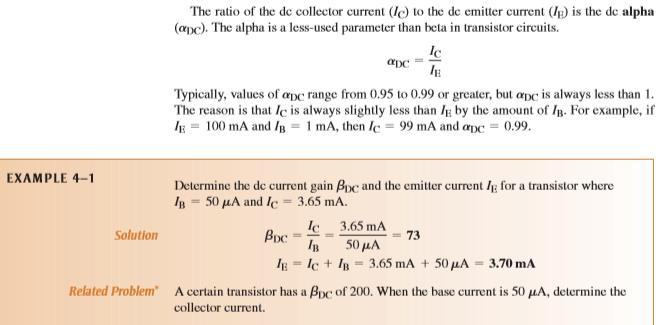
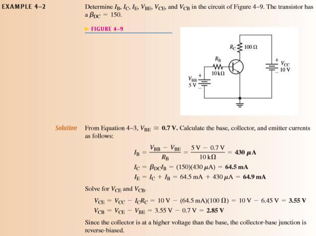
6 cotlector-base junction is reverse biased. Yet, the internal current flowing from the collector through the base region to the emitter actually is far more current than the forward-biased base-emitter junction. How can this be? Since the base region in a BJT is extremely thin and very lightly doped, the collector collects most of the electrons provided or emitted by the emitter. This accounts for why base currents are. usually quite small. When the base-emitter junction is forward biased, the base current controls the amount of collector current that is flowing within the transistor. Let's take a closer look at the emittercollector circuit. Note from the diagram that the dc source Vcc is connected in series with the collector resistor Ro The total voltage applied between the emitter and collector terminals (collector-emitter voltage, Vcÿ) of the BJT is equal to the dc voltage source minus the voltage drop across the collector resistor: Vcÿ = Vcc- IcRo If the base-emitter junction is forward biased and VcciS sufficiently high, there will be a complete path for current flow that begins from the positive terminal of Vcc through the collector resistor into the collector, and returns to the negative terminal of Vcc through the emitter. One of the vital characteristics of a BJT is that the collector current (Ic) is always much larger than the base current (IB) that controls it. The normal operating conditions for a BJT can be summarized this way: The base-emitter junction must be forward biased with a little bit of base current, Is. The collectorbase junction must be reverse biased. The following occur as a result of setting up these conditions: The emitter current, Iÿ, is equal to the sum of the base and collector currents. The collector current, Io is always much larger than the base current. Folÿula 25-1 expresses the fact that the emitter current is exactly equal to the sum of the collector and the base currents. FORMULA 25-1 Iÿ = Ic + Is The fact that Ic is always much greater than IB is expressed in terms of a ratio. Typically, Ic is between 40 and 300 times greater than Is. This ratio is expressed as the 13ÿc (de beta) or sometimes hfe. (We will use the [3do notation in our discussions, but you should expect to see the "h convention" often used in other places.) Formula 25-2 shows how you can calculate the value of dc beta when you know the values of the collector and base currents. FORMULA 25-2 ÿ3dc = Ic/I, Used in this way, [3de represents the current gain of the transistor An NPN Transistor Circuit Model Figure 25-9 shows a dc model of the NPN transistor. The model considers how the transistor operates in the three regions (cutoff, saturation, and finear). Figure 25-% models the collectoremitter junction of the transistor as a switch. If the voltage drop across the base-emitter junction is less than 0.7 V, then the switch is open (cutoff region). If the voltage drop across the baseemitter junction equals 0.7 V, then the switch is closed (saturation region). Figure 25-9b models the collector-emitter junction of the transistor 6
7 as a current-controlled current source (the base current controls the amount of collector current flowing in the circuit). Figure shows an ac model of the NPN transistor operating'in the linear region Basic Uses of the BJT Before we look at a few more details about the operation of BJTs, it is important to be able to describe basically how transistors are used. Transistors are controllers of current. The BJT uses a small amount of base current to control a larger amount of collector cun'ent. Later, you will learn that field-effect transistors use a voltage level to control the flow of current. BJTs are basically used in two ways: as switches and as amplifiers. Often, these two applications are combined in one circuit. The BJT as a Switch and Current Amplifier Figure shows a typical circuit where an NPN transistor is used as a switch and as an amplifier of current. The rectangular waveform at the input, switches between 0 V and +5 V. The LED has a forward voltage drop of 1,5 V when conducting. Resistor values are RB = 33 kÿ2 and Rc = 200 f2. The NPN transistor that is used in this circuit is a 2N3904. Let's examine how the BJT responds to the 0-V input and to the +5-V input. 1. When the input is at 0 V, the transistor is in cutoff. there is no base current flowing in the BJT (18 = 0 A) there is no collector current in the BJT (Ic = 0 A) the collector voltage is equal to the Vcc level (Vc = Vcÿ = Vcc = +5 V) (NOTE: If you measured the voltage at the collector, it may read less than 5 V since the digital multimeter provides a current conduction path and some voltage may be dropped across the LED.) the LED does not light The circuit is switched off. 2. When the input is at +5 V, the transistor is in saturation. base current is flowing in the BJT (IB > 0 A) 3. IB = (VBB -- VÿE)/Rÿ IB = (5 V- 0.7 V)/33 a IB = 130 ga 4. the collector voltage is equal to the saturation voltage of the BJT (Vc < +0.3 V) the collector current is flowing in the BJT ((Ic > 0 ma) 5. Ic = (Vcc - VD - Vcÿ(sÿ>)/gc Ic = (5 V V V)/200 :c= 16ma 6. the LED is turned on. The circuit is switched on. 7. In summary, the LED lights whenever the input waveform switches to +5 V, and the LED goes out whenever the input waveform switches to its 0 V level. The LED switches on and off at the frequency of the input waveform. At frequencies above 60 Hz, the LED visually appears to be on at all times. However, using the scope, you can observe that the LED is still turning on and off. But why do we go to the trouble of using a BJT? Why not connect the input waveform direct to the LED and simplify the circuit? Well, the reason is that the input waveform probably comes from a source that cannot provide the 16-mA current level that is required for operating most LEDs. Maybe the waveform source can provide a maximum of i ma. The BJT circuit draws only 130 ga to provide the 16-mA current for the LED. In this case, the BJT serves as a current amplifier as well as a switch. 8. The BJT as a Voltage Amplifier The circuit in Figure is a voltage amplifier. The input waveform in this example is a sinusoidal waveform that measures 2 V peak-to-peak. The values of the resistors at the base connection are selected so that the transistor is operating in the linear region (Vÿ = 2.2 V and Vc = 6 V). There is some base-bias current flowing, even when the input signal is at 0 V. Let's study how the BJT reacts to one complete cycle of the waveform at 1/4-cycle intervals At 0, the input is at 0 V. Due to the base-bias circuit, the base voltage is at 2.2 Vdo. The base current flowing is due to only the base-bias current. The BJT is conducting, so the collector 7
8 voltage is somewhere between 0 V and the +Vcc level of 12 V. Let's suppose that the base bias is adjusted so that the collector voltage is +6 V. 2. At 90, the input is at +1 V. The positive polarity of the input signal adds to the base voltage. The base voltage is now at 3.2 V. The increased base voltage causes a higher base current resulting in a larger collector current. This means the collector voltage (from collector to ground) drops to a lower level due to the I R drop across the collector resistor. Thus, less voltage is available to be dropped by the transistor. (Remember Kirchhoff's voltage law?) Let's say we find it drops down to +2 V. 3. At 180, the input is at 0 V. Again the base current flowing is due to only the base-bias current. There is less base current than while the input waveform was positive; there is less collector current, so there is a larger collector voltage. The collector voltage returns to +6 V At 270, the input is at -1 V. The negative polarity of the input signal subtracts from the basebias current set by resistors R1 and R2. The reduction in base current causes the base current IB to be lower. Subsequently, the collector current is lower resulting in an increase in the collector voltage. The collector voltage rises to a higher level, say, +10 V. 11. You can see from the resulting plot of the output waveforrn that it is a sinusoidal waveform that is 8 V peak-to-peak. This circuit is a voltage amplifier that increases the input signal from 2 Vp.p to 8 Vp.p. It is said that this amplifier has a voltage gain of 4 (8 Vp.p divided by 2 Vp.p). Also notice that this type of BJT amplifier inverts the input waveform or, in other words, shifts the waveform by 180. Even though the BJT is still a current amplifying device (IB is amplified to Ic), the surrounding circuit converted the input voltage into a current flow and used the output current (Ic) to create an output voltage. Thus making the system a voltage amplifier. After studying this chapter, you should be able to:!. Explain the derivation of the term operatlonal amplifier (op-amp) 2. Draw op-amp symbol(s) 3. Define the term differential amplifier 4. Draw a block diagram of typical circuits used in opamps 5. List the key characteristics of an ideal op-amp 6. Identify linear and nonlinear applications circuits for op-amps 7. Distinguish between inverting and noninverting op-amp circuits 8. Perform voltage gain and resistance calculations for standard inverting and noninverting op-amp circuits 9. 8
9 9
10 10
11 11
12 12
13 13
14 14
15 15
16 16
17 17
18 18
19 19
20 20
21 21
22 22
Electronic Circuits - Tutorial 07 BJT transistor 1
 Electronic Circuits - Tutorial 07 BJT transistor 1-1 / 20 - T & F # Question 1 A bipolar junction transistor has three terminals. T 2 For operation in the linear or active region, the base-emitter junction
Analog Circuits Prof. Jayanta Mukherjee Department of Electrical Engineering Indian Institute of Technology - Bombay
 Analog Circuits Prof. Jayanta Mukherjee Department of Electrical Engineering Indian Institute of Technology - Bombay Week - 08 Module - 04 BJT DC Circuits Hello, welcome to another module of this course
Figure1: Basic BJT construction.
 Chapter 4: Bipolar Junction Transistors (BJTs) Bipolar Junction Transistor (BJT) Structure The BJT is constructed with three doped semiconductor regions separated by two pn junctions, as in Figure 1(a).
Basic Electronics Prof. Dr. Chitralekha Mahanta Department of Electronics and Communication Engineering Indian Institute of Technology, Guwahati
 Basic Electronics Prof. Dr. Chitralekha Mahanta Department of Electronics and Communication Engineering Indian Institute of Technology, Guwahati Module: 2 Bipolar Junction Transistors Lecture-1 Transistor
Electronics II Lecture 2(a): Bipolar Junction Transistors
: Bipolar Junction Transistors") Lecture 2(a): Bipolar Junction Transistors A/Lectr. Khalid Shakir Dept. Of Engineering Engineering by Pearson Transistor! Transistor=Transfer+Resistor. When Transistor operates in active region its input
Lecture 2(a): Bipolar Junction Transistors A/Lectr. Khalid Shakir Dept. Of Engineering Engineering by Pearson Transistor! Transistor=Transfer+Resistor. When Transistor operates in active region its input
Bipolar Junction Transistors
 Bipolar Junction Transistors Invented in 1948 at Bell Telephone laboratories Bipolar junction transistor (BJT) - one of the major three terminal devices Three terminal devices more useful than two terminal
14. Transistor Characteristics Lab
 1 14. Transistor Characteristics Lab Introduction Transistors are the active component in various devices like amplifiers and oscillators. They are called active devices since transistors are capable of
Lecture 3: Transistors
 Lecture 3: Transistors Now that we know about diodes, let s put two of them together, as follows: collector base emitter n p n moderately doped lightly doped, and very thin heavily doped At first glance,
Chapter 3 Bipolar Junction Transistors (BJT)
") Chapter 3 Bipolar Junction Transistors (BJT) Transistors In analog circuits, transistors are used in amplifiers and linear regulated power supplies. In digital circuits they function as electrical switches,
Chapter 3 Bipolar Junction Transistors (BJT) Transistors In analog circuits, transistors are used in amplifiers and linear regulated power supplies. In digital circuits they function as electrical switches,
Chapter 3: TRANSISTORS. Dr. Gopika Sood PG Govt. College For Girls Sector -11, Chandigarh
 Chapter 3: TRANSISTORS Dr. Gopika Sood PG Govt. College For Girls Sector -11, Chandigarh OUTLINE Transistors Bipolar Junction Transistor (BJT) Operation of Transistor Transistor parameters Load Line Biasing
Transistor Characteristics
 Transistor Characteristics Topics covered in this presentation: Transistor Construction Transistor Operation Transistor Characteristics 1 of 15 The Transistor The transistor is a semiconductor device that
PHY405F 2009 EXPERIMENT 6 SIMPLE TRANSISTOR CIRCUITS
 PHY405F 2009 EXPERIMENT 6 SIMPLE TRANSISTOR CIRCUITS Due Date (NOTE CHANGE): Thursday, Nov 12 th @ 5 pm; Late penalty in effect! Most active electronic devices are based on the transistor as the fundamental
EXPERIMENT 6 REPORT Bipolar Junction Transistor (BJT) Characteristics
 Characteristics") Name & Surname: ID: Date: EXPERIMENT 6 REPORT Bipolar Junction Transistor (BJT) Characteristics Objectives: 1. To determine transistor type (npn, pnp),terminals, and material using a DMM 2. To graph the
Name & Surname: ID: Date: EXPERIMENT 6 REPORT Bipolar Junction Transistor (BJT) Characteristics Objectives: 1. To determine transistor type (npn, pnp),terminals, and material using a DMM 2. To graph the
Chapter 3-2 Semiconductor devices Transistors and Amplifiers-BJT Department of Mechanical Engineering
 MEMS1082 Chapter 3-2 Semiconductor devices Transistors and Amplifiers-BJT Bipolar Transistor Construction npn BJT Transistor Structure npn BJT I = I + E C I B V V BE CE = V = V B C V V E E Base-to-emitter
Shankersinh Vaghela Bapu Institute of Technology INDEX
 Shankersinh Vaghela Bapu Institute of Technology Diploma EE Semester III 3330905: ELECTRONIC COMPONENTS AND CIRCUITS INDEX Sr. No. Title Page Date Sign Grade 1 Obtain I-V characteristic of Diode. 2 To
4.2.2 Metal Oxide Semiconductor Field Effect Transistor (MOSFET)
") 4.2.2 Metal Oxide Semiconductor Field Effect Transistor (MOSFET) The Metal Oxide Semitonductor Field Effect Transistor (MOSFET) has two modes of operation, the depletion mode, and the enhancement mode.
4.2.2 Metal Oxide Semiconductor Field Effect Transistor (MOSFET) The Metal Oxide Semitonductor Field Effect Transistor (MOSFET) has two modes of operation, the depletion mode, and the enhancement mode.
Chapter Two "Bipolar Transistor Circuits"
 Chapter Two "Bipolar Transistor Circuits" 1.TRANSISTOR CONSTRUCTION:- The transistor is a three-layer semiconductor device consisting of either two n- and one p-type layers of material or two p- and one
EE301 Electronics I , Fall
 EE301 Electronics I 2018-2019, Fall 1. Introduction to Microelectronics (1 Week/3 Hrs.) Introduction, Historical Background, Basic Consepts 2. Rewiev of Semiconductors (1 Week/3 Hrs.) Semiconductor materials
ECE 334: Electronic Circuits Lecture 2: BJT Large Signal Model
 Faculty of Engineering ECE 334: Electronic Circuits Lecture 2: BJT Large Signal Model Agenda I & V Notations BJT Devices & Symbols BJT Large Signal Model 2 I, V Notations (1) It is critical to understand
Lecture (09) Bipolar Junction Transistor 3
 Bipolar Junction Transistor 3") Lecture (09) Bipolar Junction Transistor 3 By: Dr. Ahmed ElShafee ١ I THE BJT AS AN AMPLIFIER Amplification is the process of linearly increasing the amplitude of an electrical signal and is one of the
Lecture (09) Bipolar Junction Transistor 3 By: Dr. Ahmed ElShafee ١ I THE BJT AS AN AMPLIFIER Amplification is the process of linearly increasing the amplitude of an electrical signal and is one of the
COE/EE152: Basic Electronics. Lecture 5. Andrew Selasi Agbemenu. Outline
 COE/EE152: Basic Electronics Lecture 5 Andrew Selasi Agbemenu 1 Outline Physical Structure of BJT Two Diode Analogy Modes of Operation Forward Active Mode of BJTs BJT Configurations Early Effect Large
Emitter base bias. Collector base bias Active Forward Reverse Saturation forward Forward Cut off Reverse Reverse Inverse Reverse Forward
 SEMICONDUCTOR PHYSICS-2 [Transistor, constructional characteristics, biasing of transistors, transistor configuration, transistor as an amplifier, transistor as a switch, transistor as an oscillator] Transistor
Module 2. B.Sc. I Electronics. Developed by: Mrs. Neha S. Joshi Asst. Professor Department of Electronics Willingdon College, Sangli
 Module 2 B.Sc. I Electronics Developed by: Mrs. Neha S. Joshi Asst. Professor Department of Electronics Willingdon College, Sangli BIPOLAR JUNCTION TRANSISTOR SCOPE OF THE CHAPTER- This chapter introduces
ET215 Devices I Unit 4A
 ITT Technical Institute ET215 Devices I Unit 4A Chapter 3, Section 3.1-3.2 This unit is divided into two parts; Unit 4A and Unit 4B Chapter 3 Section 3.1 Structure of Bipolar Junction Transistors The basic
Lab 2: Discrete BJT Op-Amps (Part I)
") Lab 2: Discrete BJT Op-Amps (Part I) This is a three-week laboratory. You are required to write only one lab report for all parts of this experiment. 1.0. INTRODUCTION In this lab, we will introduce and
Lab 2: Discrete BJT Op-Amps (Part I) This is a three-week laboratory. You are required to write only one lab report for all parts of this experiment. 1.0. INTRODUCTION In this lab, we will introduce and
Student Lecture by: Giangiacomo Groppi Joel Cassell Pierre Berthelot September 28 th 2004
 Student Lecture by: Giangiacomo Groppi Joel Cassell Pierre Berthelot September 28 th 2004 Lecture outline Historical introduction Semiconductor devices overview Bipolar Junction Transistor (BJT) Field
7. Bipolar Junction Transistor
 41 7. Bipolar Junction Transistor 7.1. Objectives - To experimentally examine the principles of operation of bipolar junction transistor (BJT); - To measure basic characteristics of n-p-n silicon transistor
Lecture 24: Bipolar Junction Transistors (1) Bipolar Junction Structure, Operating Regions, Biasing
 Bipolar Junction Structure, Operating Regions, Biasing") Lecture 24: Bipolar Junction Transistors (1) Bipolar Junction Structure, Operating Regions, Biasing BJT Structure the BJT is formed by doping three semiconductor regions (emitter, base, and collector)
Lecture 24: Bipolar Junction Transistors (1) Bipolar Junction Structure, Operating Regions, Biasing BJT Structure the BJT is formed by doping three semiconductor regions (emitter, base, and collector)
Physics of Bipolar Transistor
 Physics of Bipolar Transistor Motivations - In many electronic applications, amplifier is the most fundamental building block. Ex Audio amplifier: amplifies electric signal to drive a speaker RF Power
I C I E =I B = I C 1 V BE 0.7 V
 Guide to NPN Amplifier Analysis Jason Woytowich 1. Transistor characteristics A BJT has three operating modes cutoff, active, and saturation. For applications, like amplifiers, where linear characteristics
Analog Electronic Circuits Lab-manual
 2014 Analog Electronic Circuits Lab-manual Prof. Dr Tahir Izhar University of Engineering & Technology LAHORE 1/09/2014 Contents Experiment-1:...4 Learning to use the multimeter for checking and indentifying
Field Effect Transistors
 Field Effect Transistors Purpose In this experiment we introduce field effect transistors (FETs). We will measure the output characteristics of a FET, and then construct a common-source amplifier stage,
Chapter 6: Transistors and Gain
 I. Introduction Chapter 6: Transistors and Gain This week we introduce the transistor. Transistors are three-terminal devices that can amplify a signal and increase the signal s power. The price is that
Lecture 9 Transistors
 Lecture 9 Transistors Physics Transistor/transistor logic CMOS logic CA 1947 http://www.extremetech.com/extreme/164301-graphenetransistors-based-on-negative-resistance-could-spell-theend-of-silicon-and-semiconductors
Electronic Circuits ELECTRONIC CIRCUITS. Subject Code: 10CS32 I.A. Marks : 25 Hours/Week : 04 Exam Hours: 03 Total Hours : 52 Exam Marks: 100
 ELECTRONIC CIRCUITS Subject Code: I.A. Marks : 5 Hours/Week : 04 Exam Hours: 03 Total Hours : 5 Exam Marks: 00 UNIT PART - A 7 Hours Transistors, UJTs, and Thyristors: Operating Point, Common-EmitterConfiguration,
KOM2751 Analog Electronics :: Dr. Muharrem Mercimek :: YTU - Control and Automation Dept. 1 2 (CONT D - II) DIODE APPLICATIONS
 DIODE APPLICATIONS") KOM2751 Analog Electronics :: Dr. Muharrem Mercimek :: YTU - Control and Automation Dept. 1 2 (CONT D - II) DIODE APPLICATIONS Most of the content is from the textbook: Electronic devices and circuit theory,
KOM2751 Analog Electronics :: Dr. Muharrem Mercimek :: YTU - Control and Automation Dept. 1 2 (CONT D - II) DIODE APPLICATIONS Most of the content is from the textbook: Electronic devices and circuit theory,
UNIT-1 Bipolar Junction Transistors. Text Book:, Microelectronic Circuits 6 ed., by Sedra and Smith, Oxford Press
 UNIT-1 Bipolar Junction Transistors Text Book:, Microelectronic Circuits 6 ed., by Sedra and Smith, Oxford Press Figure 6.1 A simplified structure of the npn transistor. Microelectronic Circuits, Sixth
BJT. Bipolar Junction Transistor BJT BJT 11/6/2018. Dr. Satish Chandra, Assistant Professor, P P N College, Kanpur 1
 BJT Bipolar Junction Transistor Satish Chandra Assistant Professor Department of Physics P P N College, Kanpur www.satish0402.weebly.com The Bipolar Junction Transistor is a semiconductor device which
An Introduction to Bipolar Junction Transistors. Prepared by Dr Yonas M Gebremichael, 2005
 An Introduction to Bipolar Junction Transistors Transistors Transistors are three port devices used in most integrated circuits such as amplifiers. Non amplifying components we have seen so far, such as
Semiconductors, ICs and Digital Fundamentals
 Semiconductors, ICs and Digital Fundamentals The Diode The semiconductor phenomena. Diode performance with ac and dc currents. Diode types: General purpose LED Zener The Diode The semiconductor phenomena
EXPERIMENT 5 CURRENT AND VOLTAGE CHARACTERISTICS OF BJT
 EXPERIMENT 5 CURRENT AND VOLTAGE CHARACTERISTICS OF BJT 1. OBJECTIVES 1.1 To practice how to test NPN and PNP transistors using multimeter. 1.2 To demonstrate the relationship between collector current
Exercise 2: Collector Current Versus Base Current
 Exercise 2: Collector Current Versus Base Current EXERCISE OBJECTIVE When you have completed this exercise, you will be able to demonstrate the relationship of collector current to base current by using
Analog Electronics. Electronic Devices, 9th edition Thomas L. Floyd Pearson Education. Upper Saddle River, NJ, All rights reserved.
 Analog Electronics BJT Structure The BJT has three regions called the emitter, base, and collector. Between the regions are junctions as indicated. The base is a thin lightly doped region compared to the
Lecture 12. Bipolar Junction Transistor (BJT) BJT 1-1
 BJT 1-1") Lecture 12 Bipolar Junction Transistor (BJT) BJT 1-1 Course Info Lecture hours: 4 Two Lectures weekly (Saturdays and Wednesdays) Location: K2 Time: 1:40 pm Tutorial hours: 2 One tutorial class every week
Lecture 12 Bipolar Junction Transistor (BJT) BJT 1-1 Course Info Lecture hours: 4 Two Lectures weekly (Saturdays and Wednesdays) Location: K2 Time: 1:40 pm Tutorial hours: 2 One tutorial class every week
o Semiconductor Diode Symbol: The cathode contains the N-type material and the anode contains the P-type material.
 Cornerstone Electronics Technology and Robotics I Week 16 Diodes and Transistor Switches Administration: o Prayer o Turn in quiz Review: o Design and wire a voltage divider that divides your +9 V voltage
Lab 4. Transistor as an amplifier, part 2
 Lab 4 Transistor as an amplifier, part 2 INTRODUCTION We continue the bi-polar transistor experiments begun in the preceding experiment. In the common emitter amplifier experiment, you will learn techniques
ELEC 2210 EXPERIMENT 7 The Bipolar Junction Transistor (BJT)
") ELEC 2210 EXPERIMENT 7 The Bipolar Junction Transistor (BJT) Objectives: The experiments in this laboratory exercise will provide an introduction to the BJT. You will use the Bit Bucket breadboarding system
ELEC 2210 EXPERIMENT 7 The Bipolar Junction Transistor (BJT) Objectives: The experiments in this laboratory exercise will provide an introduction to the BJT. You will use the Bit Bucket breadboarding system
The Common Emitter Amplifier Circuit
 The Common Emitter Amplifier Circuit In the Bipolar Transistor tutorial, we saw that the most common circuit configuration for an NPN transistor is that of the Common Emitter Amplifier circuit and that
Review Energy Bands Carrier Density & Mobility Carrier Transport Generation and Recombination
 Review Energy Bands Carrier Density & Mobility Carrier Transport Generation and Recombination Current Transport: Diffusion, Thermionic Emission & Tunneling For Diffusion current, the depletion layer is
UNIT-III Bipolar Junction Transistor
 DC UNT-3.xplain the construction and working of JT. UNT- ipolar Junction Transistor A bipolar (junction) transistor (JT) is a three-terminal electronic device constructed of doped semiconductor material
.dc Vcc Ib 0 50uA 5uA
 EE 2274 BJT Biasing PreLab: 1. Common Emitter (CE) Transistor Characteristics curve Generate the characteristics curves for a 2N3904 in LTspice by plotting Ic by sweeping Vce over a set of Ib steps. Label
ITT Technical Institute. ET215 Devices 1. Unit 6 Chapter 3, Sections
 ITT Technical Institute ET215 Devices 1 Unit 6 Chapter 3, Sections 3.7-3.9 Chapter 3 Section 3.7 The Bipolar Transistor as a Switch Objectives: Explain how a transistor can be used as a switch 1. Compute
Transistors and Applications
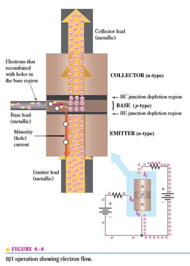
 Chapter 17 Transistors and Applications DC Operation of Bipolar Junction Transistors (BJTs) The bipolar junction transistor (BJT) is constructed with three doped semiconductor regions separated by two
Experiments #6. Differential Amplifier
 Experiments #6 Differential Amplifier 1) Objectives: To understand the DC and AC operation of a differential amplifier. To measure DC voltages and currents in differential amplifier. To obtain measured
The BJT Transistor Theory
 The BJT Transistor Theory Giorgos V. Lazaridis Dipl.-ing www.pcbheaven.com Copyright 2013-2014 Revision A Disclaimer The information provided in this e-book is intended to provide helpful information on
5.1 BJT Device Structure and Physical Operation
 11/28/2004 section 5_1 BJT Device Structure and Physical Operation blank 1/2 5.1 BJT Device Structure and Physical Operation Reading Assignment: pp. 377-392 Another kind of transistor is the Bipolar Junction
Gechstudentszone.wordpress.com
 Unit 1: Transistor, UJT s, and Thyristors In the Diode tutorials we saw that simple diodes are made up from two pieces of semiconductor material, either silicon or germanium to form a simple PN-junction
Unit/Standard Number. LEA Task # Alignment
 1 Secondary Competency Task List 100 SAFETY 101 Demonstrate an understanding of State and School safety regulations. 102 Practice safety techniques for electronics work. 103 Demonstrate an understanding
Exercises 6.1, 6.2, 6.3 (page 315 on 7 th edition textbook)
") Exercises 6.1, 6.2, 6.3 (page 315 on 7 th edition textbook) Recapitulation and Equivalent Circuit Models Previous slides present first order BJT model. Assumes npn transistor in active mode. Basic relationship
Exercises 6.1, 6.2, 6.3 (page 315 on 7 th edition textbook) Recapitulation and Equivalent Circuit Models Previous slides present first order BJT model. Assumes npn transistor in active mode. Basic relationship
ME 4447 / 6405 Student Lecture. Transistors. Abiodun Otolorin Michael Abraham Waqas Majeed
 ME 4447 / 6405 Student Lecture Transistors Abiodun Otolorin Michael Abraham Waqas Majeed Lecture Overview Transistor? History Underlying Science Properties Types of transistors Bipolar Junction Transistors
EE301 Electronics I , Fall
 EE301 Electronics I 2018-2019, Fall 1. Introduction to Microelectronics (1 Week/3 Hrs.) Introduction, Historical Background, Basic Consepts 2. Rewiev of Semiconductors (1 Week/3 Hrs.) Semiconductor materials
Electrical, Electronic and Communications Engineering Technology/Technician CIP Task Grid
 Secondary Task List 100 SAFETY 101 Describe OSHA safety regulations. 102 Identify, select, and demonstrate proper hand tool use for electronics work. 103 Recognize the types and usages of fire extinguishers.
Module 04.(B1) Electronic Fundamentals
 Electronic Fundamentals") 1.1a. Semiconductors - Diodes. Module 04.(B1) Electronic Fundamentals Question Number. 1. What gives the colour of an LED?. Option A. The active element. Option B. The plastic it is encased in. Option
1.1a. Semiconductors - Diodes. Module 04.(B1) Electronic Fundamentals Question Number. 1. What gives the colour of an LED?. Option A. The active element. Option B. The plastic it is encased in. Option
Chapter 5 Transistor Bias Circuits
 Chapter 5 Transistor Bias Circuits Objectives Discuss the concept of dc biasing of a transistor for linear operation Analyze voltage-divider bias, base bias, and collector-feedback bias circuits. Basic
ECEN 325 Lab 7: Characterization and DC Biasing of the BJT
 ECEN 325 Lab 7: Characterization and DC Biasing of the BJT 1 Objectives The purpose of this lab is to characterize NPN and PNP bipolar junction transistors (BJT), and to analyze and design DC biasing circuits
EE 330 Laboratory 8 Discrete Semiconductor Amplifiers
 EE 330 Laboratory 8 Discrete Semiconductor Amplifiers Fall 2018 Contents Objective:...2 Discussion:...2 Components Needed:...2 Part 1 Voltage Controlled Amplifier...2 Part 2 A Nonlinear Application...3
Physics 222. Lab 5: Characterizing a transistor, and using it to control motor speeds. Objectives:
 Fresh page; your name, your partners full names, date, title. You may copy the objectives, introduction, equipment, safety and procedure sections, or you may print this handout and neatly tape in these
Transistor Biasing and Operational amplifier fundamentals. OP-amp Fundamentals and its DC characteristics. BJT biasing schemes
 Lab 1 Transistor Biasing and Operational amplifier fundamentals Experiment 1.1 Experiment 1.2 BJT biasing OP-amp Fundamentals and its DC characteristics BJT biasing schemes 1.1 Objective 1. To sketch potential
ES330 Laboratory Experiment No. 9 Bipolar Differential Amplifier [Reference: Sedra/Smith (Chapter 9; Section 9.2; pp )]
![ES330 Laboratory Experiment No. 9 Bipolar Differential Amplifier [Reference: Sedra/Smith (Chapter 9; Section 9.2; pp )]](/thumbs/84/89341671.jpg "ES330 Laboratory Experiment No. 9 Bipolar Differential Amplifier [Reference: Sedra/Smith (Chapter 9; Section 9.2; pp )]") ES330 Laboratory Experiment No. 9 Bipolar Differential Amplifier [Reference: Sedra/Smith (Chapter 9; Section 9.2; pp. 614-627)] Objectives: 1. Explore the operation of a bipolar junction transistor differential
ES330 Laboratory Experiment No. 9 Bipolar Differential Amplifier [Reference: Sedra/Smith (Chapter 9; Section 9.2; pp. 614-627)] Objectives: 1. Explore the operation of a bipolar junction transistor differential
Bipolar Junction Transistor (BJT)
") Bipolar Junction Transistor (BJT) 1 Objectives To understand the structure of BJT. To explain and analyze the basic transistor circuits. To use transistors as an amplifier and electronic switch. To design
Bipolar Junction Transistor (BJT) 1 Objectives To understand the structure of BJT. To explain and analyze the basic transistor circuits. To use transistors as an amplifier and electronic switch. To design
UNIT 3 Transistors JFET
 UNIT 3 Transistors JFET Mosfet Definition of BJT A bipolar junction transistor is a three terminal semiconductor device consisting of two p-n junctions which is able to amplify or magnify a signal. It
Power Bipolar Junction Transistors (BJTs)
") ECE442 Power Semiconductor Devices and Integrated Circuits Power Bipolar Junction Transistors (BJTs) Zheng Yang (ERF 3017, email: yangzhen@uic.edu) Power Bipolar Junction Transistor (BJT) Background The
ECE442 Power Semiconductor Devices and Integrated Circuits Power Bipolar Junction Transistors (BJTs) Zheng Yang (ERF 3017, email: yangzhen@uic.edu) Power Bipolar Junction Transistor (BJT) Background The
Chapter 3. Bipolar Junction Transistors
 Chapter 3. Bipolar Junction Transistors Outline: Fundamental of Transistor Common-Base Configuration Common-Emitter Configuration Common-Collector Configuration Introduction The transistor is a three-layer
EE 330 Laboratory 8 Discrete Semiconductor Amplifiers
 EE 330 Laboratory 8 Discrete Semiconductor Amplifiers Fall 2017 Contents Objective:... 2 Discussion:... 2 Components Needed:... 2 Part 1 Voltage Controlled Amplifier... 2 Part 2 Common Source Amplifier...
CHARACTERIZATION OF OP-AMP
 EXPERIMENT 4 CHARACTERIZATION OF OP-AMP OBJECTIVES 1. To sketch and briefly explain an operational amplifier circuit symbol and identify all terminals. 2. To list the amplifier stages in a typical op-amp
In this lecture we will begin a new topic namely the Metal-Oxide-Semiconductor Field Effect Transistor.
 Solid State Devices Dr. S. Karmalkar Department of Electronics and Communication Engineering Indian Institute of Technology, Madras Lecture - 38 MOS Field Effect Transistor In this lecture we will begin
Page 1 of 7. Power_AmpFal17 11/7/ :14
 ECE 3274 Power Amplifier Project (Push Pull) Richard Cooper 1. Objective This project will introduce two common power amplifier topologies, and also illustrate the difference between a Class-B and a Class-AB
Concepts to be Covered
 Introductory Medical Device Prototyping Analog Circuits Part 2 Semiconductors, http://saliterman.umn.edu/ Department of Biomedical Engineering, University of Minnesota Concepts to be Covered Semiconductors
BJT Characteristics & Common Emitter Transistor Amplifier
 LAB #07 Objectives 1. To graph the collector characteristics of a transistor. 2. To measure AC and DC voltages in a common-emitter amplifier. Theory BJT A bipolar (junction) transistor (BJT) is a three-terminal
Lab 3: BJT Digital Switch
 Lab 3: BJT Digital Switch Objectives The purpose of this lab is to acquaint you with the basic operation of bipolar junction transistor (BJT) and to demonstrate its functionality in digital switching circuits.
The first transistor. (Courtesy Bell Telephone Laboratories.)
") Fig. 3.1 The first transistor. (Courtesy Bell Telephone Laboratories.) Fig. 3.2 Types of transistors: (a) pnp; (b) npn. : (a) pnp; : (b) npn Fig. 3.3 Forward-biased junction of a pnp transistor. Fig. 3.4
Fig. 3.1 The first transistor. (Courtesy Bell Telephone Laboratories.) Fig. 3.2 Types of transistors: (a) pnp; (b) npn. : (a) pnp; : (b) npn Fig. 3.3 Forward-biased junction of a pnp transistor. Fig. 3.4
Lesson 08. Bipolar & Field Effect Transistors
 Lesson 08 Sierra College CIE-01 Jim Weir 530.272.2203 jweir43@gmail.com www.rstengineering.com/sierra Bipolar & Field Effect Transistors Bipolar Transistors. Bipolar transistors are so named because they
PREVIEW COPY. Amplifiers. Table of Contents. Introduction to Amplifiers...3. Single-Stage Amplifiers...19
 Amplifiers Table of Contents Lesson One Lesson Two Lesson Three Introduction to Amplifiers...3 Single-Stage Amplifiers...19 Amplifier Performance and Multistage Amplifiers...35 Lesson Four Op Amps...51
Field Effect Transistors (npn)
") Field Effect Transistors (npn) gate drain source FET 3 terminal device channel e - current from source to drain controlled by the electric field generated by the gate base collector emitter BJT 3 terminal
Field Effect Transistors (npn) gate drain source FET 3 terminal device channel e - current from source to drain controlled by the electric field generated by the gate base collector emitter BJT 3 terminal
THE METAL-SEMICONDUCTOR CONTACT
 THE METAL-SEMICONDUCTOR CONTACT PROBLEM 1 To calculate the theoretical barrier height, built-in potential barrier, and maximum electric field in a metal-semiconductor diode for zero applied bias. Consider
Electronics Prof D. C. Dube Department of Physics Indian Institute of Technology, Delhi
 Electronics Prof D. C. Dube Department of Physics Indian Institute of Technology, Delhi Module No. # 04 Feedback in Amplifiers, Feedback Configurations and Multi Stage Amplifiers Lecture No. # 03 Input
4 Transistors. 4.1 IV Relations
 4 Transistors Due date: Sunday, September 19 (midnight) Reading (Bipolar transistors): HH sections 2.01-2.07, (pgs. 62 77) Reading (Field effect transistors) : HH sections 3.01-3.03, 3.11-3.12 (pgs. 113
I1 19u 5V R11 1MEG IDC Q7 Q2N3904 Q2N3904. Figure 3.1 A scaled down 741 op amp used in this lab
 Lab 3: 74 Op amp Purpose: The purpose of this laboratory is to become familiar with a two stage operational amplifier (op amp). Students will analyze the circuit manually and compare the results with SPICE.
FIELD EFFECT TRANSISTORS MADE BY : GROUP (13)/PM
/PM") FIELD EFFECT TRANSISTORS MADE BY : GROUP (13)/PM THE FIELD EFFECT TRANSISTOR (FET) In 1945, Shockley had an idea for making a solid state device out of semiconductors. He reasoned that a strong electrical
FIELD EFFECT TRANSISTORS MADE BY : GROUP (13)/PM THE FIELD EFFECT TRANSISTOR (FET) In 1945, Shockley had an idea for making a solid state device out of semiconductors. He reasoned that a strong electrical
Experiment (1) Principles of Switching
 Principles of Switching") Experiment (1) Principles of Switching Introduction When you use microcontrollers, sometimes you need to control devices that requires more electrical current than a microcontroller can supply; for this,
Experiment (1) Principles of Switching Introduction When you use microcontrollers, sometimes you need to control devices that requires more electrical current than a microcontroller can supply; for this,
Semiconductor analyser AS4002P User Manual
 Semiconductor analyser AS4002P User Manual Copyright Ormelabs (C) 2010 http://www.ormelabs.com 1 CONTENTS SECTION Page SECTION 1: Introduction... 3 SECTION 2: Features... 3 SECTION 3: Component analysis...
Transistors CHAPTER 3.1 INTRODUCTION
 CHAPTER 3 Bipolar Junction Transistors 3. INTRODUCTION During the period 904 947, the vacuum tube was undoubtedly the electronic device of interest and development. In 904, the vacuum-tube diode was introduced
Revised April Unit/Standard Number. Proficiency Level Achieved: (X) Indicates Competency Achieved to Industry Proficiency Level
 Indicates Competency Achieved to Industry Proficiency Level") Unit/Standard Number Electrical, Electronic and Communications Engineering Technology/Technician CIP 15.0303 Task Grid Secondary Competency Task List 100 SAFETY 101 Demonstrate an understanding of state,
Unit/Standard Number Electrical, Electronic and Communications Engineering Technology/Technician CIP 15.0303 Task Grid Secondary Competency Task List 100 SAFETY 101 Demonstrate an understanding of state,
Chapter Three " BJT Small-Signal Analysis "
 Chapter Three " BJT Small-Signal Analysis " We now begin to examine the small-signal ac response of the BJT amplifier by reviewing the models most frequently used to represent the transistor in the sinusoidal
ECE 440 Lecture 29 : Introduction to the BJT-I Class Outline:
 ECE 440 Lecture 29 : Introduction to the BJT-I Class Outline: Narrow-Base Diode BJT Fundamentals BJT Amplification Things you should know when you leave Key Questions How does the narrow-base diode multiply
Electronic Circuits EE359A
 Electronic Circuits EE359A Bruce McNair B206 bmcnair@stevens.edu 201-216-5549 Lecture 4 0 Bipolar Junction Transistors (BJT) Small Signal Analysis Graphical Analysis / Biasing Amplifier, Switch and Logic
Electronic Circuits II Laboratory 01 Voltage Divider Bias
 Electronic Circuits II Laboratory 01 Voltage Divider Bias # Student ID Student Name Grade (10) 1 Instructor signature 2 3 4 5 Delivery Date -1 / 8 - Objective The objective of this exercise is to examine
Difference between BJTs and FETs. Junction Field Effect Transistors (JFET)
") Difference between BJTs and FETs Transistors can be categorized according to their structure, and two of the more commonly known transistor structures, are the BJT and FET. The comparison between BJTs
Difference between BJTs and FETs Transistors can be categorized according to their structure, and two of the more commonly known transistor structures, are the BJT and FET. The comparison between BJTs
Technological Studies. - Applied Electronics (H) TECHNOLOGICAL STUDIES HIGHER APPLIED ELECTRONICS. Transistors. Craigmount High School 1
 TECHNOLOGICAL STUDIES HIGHER APPLIED ELECTRONICS. Transistors. Craigmount High School 1") TECHNOLOGICAL STUDIES HIGHER APPLIED ELECTRONICS Transistors Craigmount High School 1 APPLIED ELECTRONICS Outcome 1 - Design and construct electronic systems to meet given specifications When you have
TECHNOLOGICAL STUDIES HIGHER APPLIED ELECTRONICS Transistors Craigmount High School 1 APPLIED ELECTRONICS Outcome 1 - Design and construct electronic systems to meet given specifications When you have
ECE 121 Electronics (1)
") ECE 121 Electronics (1) Lec. 1: Introduction to BJT Instructor Dr. Maher Abdelrasoul http://www.bu.edu.eg/staff/mahersalem3 1 Outline Course Information Course Objectives BJT Introduction Transistor Construction
ECE 121 Electronics (1) Lec. 1: Introduction to BJT Instructor Dr. Maher Abdelrasoul http://www.bu.edu.eg/staff/mahersalem3 1 Outline Course Information Course Objectives BJT Introduction Transistor Construction