Recent development of large-scale reconfigurable data-paths using RSFQ circuits
|
|
|
- Irma Harrison
- 5 years ago
- Views:
Transcription


1 Yokohama National University 21 st International Symposium on Superconductivity Tsukuba, Japan October 27-29, 29, 2008 Recent development of large-scale reconfigurable data-paths using RSFQ circuits Nobuyuki Yoshikawa Department of Electrical and Computer Engineering, Yokohama National University, Yokohama, Japan Coworker H. Park, H. Hara, K. Taketomi, T. Kainuma, Y. Yamanashi Yokohama National University I. Kataeva, R. Kasagi, S. Iwasaki, H. Akaike, A. Fujimaki, M. Tanaka, K. Obata, Y. Ito, K. Takagi, N. Takagi Nagoya University H. Honda, K. Inoue, K. Murakami Kyusyu University S. Nagasawa, M. Hidaka SRL/ISTEC
2 Outline of This Talk Background Architecture Target system Component developments Floating-point adders/multipliers (FPA/FPU) 2 x 2 RDP New process and cell library Road map Summary
3 Demand on High-Performance Computer Calculation amount of electronic structure of molecules l using the molecular l orbital method O(N 4 ) A molecule with 1000 atoms 600 TB of ERI calculations l composed of a lot of product-sum operations
4 Breakdown of Moore s Law Trends of the clock frequency of recent microprocessors [GHz] 5 3 Pentium 4 uency Cloc ck freq x / year Xeon Pentium III Celeron 1.1x / year intel.com/


5 Problem in High-Performance Computers and Our Approach Large power consumption Memory wall problem (Single Flux Quantum circuits + new architecture) solves these problems Josephson junction 0 = h/2e = 2.07 mv. ps
 S using RSFQ Circuits A lot of")


6 Large-Scale Reconfigurable Data-Path (LSRDP) S using RSFQ Circuits A lot of FPUs + Reconfigurable network The data are directly transferred between FPUs. Reduction of memory wall problem N. Takagi et al. IEICE Technical Report, SCE , January 2007.
=(((3+2*p*(4*pax*pbx+pbx**2+pax**2*(1+2*p*pbx**2)))*(3+2*q*(4*qcx*qdx+qdx**2+qcx**2*(1+2*q*qdx**2)))*f(0,t))/(p**2*q**2)+(4*(3+2*p*(4*pax*pbx+pbx*")
))*f(1,t))/(p*q*(p+q))(8*(pax+pbx)*(3+2*p*pax*pbx)*(qcx+qdx)*(3+2*q*qcx*qdx)*(((p+q)*f(1,t))+2*p*pqx**2*q*f(2,t)))/(p*q*(p+q)**2)+(2*(3+2*p*(4*pax*pbx+pbx**2+pax**2")
))*(((p+q)*f(1,t))+2*p*PQx**2*q*f(2,t)))/(p**2*q*(p+q)**2)+(4*(3+2*p*(4*PAx*PBx+PBx**2+PAx**2*(1+2*p*PBx**2)))*PQx*(QCx+QDx)*(3*(p+q)*f(")
*(3+2*p*PAx*PBx)*PQx*(3+q*(QCx**2+4*QCx*QDx+QDx**2))*(3*(p+q)*f(2,t)+2*p*PQx**2*q*f(3,t)))/(q*(p+q)**3)(4*(PAx+PBx)*PQx*(3+2*q*(4*QCx*QDx+QDx**2+QCx**2*(")
7 Example of Application of LSRDP while (I < 1000): Electron repulsion integral calculations of molecular orbit tei(4,4,4,4)=(((3+2*p*(4*pax*pbx+pbx**2+pax**2*(1+2*p*pbx**2)))*(3+2*q*(4*qcx*qdx+qdx**2+qcx**2*(1+2*q*qdx**2)))*f(0,t))/(p**2*q**2)+(4*(3+2*p*(4*pax*pbx+pbx* *2+PAx**2*(1+2*p*PBx**2)))*PQx*(QCx+QDx)*(3+2*q*QCx*QDx)*f(1,t))/(p*q*(p+q))(4*(PAx+PBx)*(3+2*p*PAx*PBx)*PQx*(3+2*q*(4*QCx*QDx+QDx**2+QCx**2*(1+2*q*QDx**2 )))*f(1,t))/(p*q*(p+q))(8*(pax+pbx)*(3+2*p*pax*pbx)*(qcx+qdx)*(3+2*q*qcx*qdx)*(((p+q)*f(1,t))+2*p*pqx**2*q*f(2,t)))/(p*q*(p+q)**2)+(2*(3+2*p*(4*pax*pbx+pbx**2+pax**2 *(1+2*p*PBx**2)))*(3+q*(QCx**2+4*QCx*QDx+QDx**2))*(((p+q)*f(1,t))+2*p*PQx**2*q*f(2,t)))/(p*q**2*(p+q)**2)+(2*(3+p*(PAx**2+4*PAx*PBx+PBx**2))*(3+2*q*(4*QCx*QDx+Q Dx**2+QCx**2*(1+2*q*QDx**2)))*(((p+q)*f(1,t))+2*p*PQx**2*q*f(2,t)))/(p**2*q*(p+q)**2)+(4*(3+2*p*(4*PAx*PBx+PBx**2+PAx**2*(1+2*p*PBx**2)))*PQx*(QCx+QDx)*(3*(p+q)*f( 2,t)+2*p*PQx**2*q*f(3,t)))/(q*(p+q)**3) +(8*(3+p*(PAx**2+4*PAx*PBx+PBx**2))*PQx*(QCx+QDx)*(3+2*q*QCx*QDx)*(3*(p+q)*f(2,t)+2*p*PQx**2*q*f(3,t)))/(p*(p+q)**3)(8*(PAx+ PBx)*(3+2*p*PAx*PBx)*PQx*(3+q*(QCx**2+4*QCx*QDx+QDx**2))*(3*(p+q)*f(2,t)+2*p*PQx**2*q*f(3,t)))/(q*(p+q)**3)(4*(PAx+PBx)*PQx*(3+2*q*(4*QCx*QDx+QDx**2+QCx**2*( 1+2*q*QDx**2)))*(3*(p+q)*f(2,t)+2*p*PQx**2*q*f(3,t)))/(p*(p+q)**3)+((3+2*p*(4*PAx*PBx+PBx**2+PAx**2*(1+2*p*PBx**2)))*(3*(p+q)**2*f(2,t)+4*p*PQx**2*q*(3*(p+q)*f(3,t)+p* PQx**2*q*f(4,t))))/(q**2*(p+q)**4)(8*(PAx+PBx)*(3+2*p*PAx*PBx)*(QCx+QDx)*(3*(p+q)**2*f(2,t)+4*p*PQx**2*q*(3*(p+q)*f(3,t)+p*PQx**2*q*f(4,t))))/(q*(p+q)**4)(8*(PAx+PBx)*( QCx+QDx)*(3+2*q*QCx*QDx)*(3*(p+q)**2*f(2,t)+4*p*PQx**2*q*(3*(p+q)*f(3,t)+p*PQx**2*q*f(4,t))))/(p*(p+q)**4)+(4*(3+p*(PAx**2+4*PAx*PBx+PBx**2))*(3+q*(QCx**2+4*QCx* QDx+QDx**2))*(3*(p+q)**2*f(2,t)+4*p*PQx**2*q*(3*(p+q)*f(3,t)+p*PQx**2*q*f(4,t))))/(p*q*(p+q)**4)+((3+2*q*(4*QCx*QDx+QDx**2+QCx**2*(1+2*q*QDx**2)))*(3*(p+q)**2*f(2,t) +4*p*PQx**2*q*(3*(p+q)*f(3,t)+p*PQx**2*q*f(4,t))))/(p**2*(p+q)**4)(4*p*(PAx+PBx)*(3+2*p*PAx*PBx)*PQx*(15*(p+q)**2*f(3,t)+4*p*PQx**2*q*(5*(p+q)*f(4,t)+p*PQx**2*q*f(5,t)) ))/(q*(p+q)**5)+(8*(3+p*(pax**2+4*pax*pbx+pbx**2))*pqx*(qcx+qdx)*(15*(p+q)**2*f(3,t)+4*p*pqx**2*q*(5*(p+q)*f(4,t)+p*pqx**2*q*f(5,t))))/(p+q)**5+(4*pqx*q*(qcx+qdx)*( 3+2*q*QCx*QDx)*(15*(p+q)**2*f(3,t)+4*p*PQx**2*q*(5*(p+q)*f(4,t)+p*PQx**2*q*f(5,t))))/(p*(p+q)**5)(8*(PAx+PBx)*PQx*(3+q*(QCx**2+4*QCx*QDx+QDx**2))*(15*(p+q)**2*f(3,t )+4*p*PQx**2*q*(5*(p+q)*f(4,t)+p*PQx**2*q*f(5,t))))/(p+q)**5+(8*(PAx+PBx)*(QCx+QDx)*(15*(p+q)**3*f(3,t)+30*p*PQx**2*q*(p+q)*(3*(p+q)*f(4,t)+2*p*PQx**2*q*f(5,t))8*p**3*P Qx**6*q**3*f(6,t)))/(p+q)**6+(2*(3+p*(PAx**2+4*PAx*PBx+PBx**2))*(15*(p+q)**3*f(3,t)30*p*PQx**2*q*(p+q)*(3*(p+q)*f(4,t)+2*p*PQx**2*q*f(5,t))+8*p**3*PQx**6*q**3*f(6,t)))/( q*(p+q)**6)+(2*(3+q*(qcx**2+4*qcx*qdx+qdx**2))*(15*(p+q)**3*f(3,t)30*p*pqx**2*q*(p+q)*(3*(p+q)*f(4,t)+2*p*pqx**2*q*f(5,t))+8*p**3*pqx**6*q**3*f(6,t)))/(p*(p+q)**6) 787 MUL, 261 ADD, 69 FUNC I = I+1: Data-flow graph mapped to the LSRDP


8 LSRDP Architecture: Suitable for RSFQ Circuits Data flow in one direction. No loop structure. Need high throughput. Latency is not so important. Suitable for bit-serial processing. Reduced requirement on memory band width. High switching activity. Heating is serious in semiconductor circuits
9 Application Fields of LSRDP Processors Molecular orbit calculation Diffusion equation Wave equation Poisson equation etc.

 p (4GFLOPS/FPU)... ORN ORN.")
 4MCM SMAC Memory band width per")
10 Target System: 10-TFLOPS RSFQ-LSRDP Computer 4.2 K 2TB memory module (FB-DIMM [DDR3@1333MHz, 128GB] 16 modules) CMOS CPU (1chip) ORN FPU... ORN : : : : SFQ 0.5um process SFQ RDP (32FPU 32chips) p (4GFLOPS/FPU)... ORN ORN... SFQ Streaming Buffer (64Kb 2chips) : : : SMAC SMAC SB... : 1024FPU@MCM (34chips) 4MCM SMAC Memory band width per MCM:256GB/s (=16GB/s 16 channels)
11 Organization of the Project Profs. K. Murakami, H. Honda (Kyushu Univ.) LSRDP architecture, compiler, algorithm Profs. N. Takagi, K. Takagi (Nagoya Univ.) CAD for logic design, arithmetic circuits Prof. N. Yoshikawa (Yokohama National Univ.) RSFQ-FPU chip, cell library Profs. A. Fujimaki, H. Akaike (Nagoya Univ.) Network, RSFQ-LSRDP chip, cell library Dr. S. Nagasawa (SRL) Advanced process
12 Component Development Floating-point adder (FPA) Floating-point multiplier (FPM) Operand routing network (ORN) 2 x 2 LSRDP prototype


")
 Example")


13 Floating-Point Numbers S: Sign (-1) S F 2 E E: Exponent F: Significand or Fraction S(1bit) E(8 bit) F(23 bit) Example (single precision, 32 bit): Data format in IEEE754 standard Sign Exponent Fraction Half-precision Single-precision Double-precision
14 Bit-Serial Floating-Point Calculation Two bit-serial data-paths are used for the calculation of significand and exponent. n f LSB Significand MSB n e Sign LSB Exponent MSB t
15 Timing Parameters in Bit-Serial Calculation Input (clock) (clock) Output MSB Input LSB (data) Operation Unit (data) MSB Output LSB Time Input (clock) (data) LSB Input 1 MSB LSB Input 2 MSB LSB Input 3 MSB C. Minimum interval Output (clock) (data) A. Skew LSB Output 1 MSB B. Latency
 2.")
 3.")
 +(11.00110 2 4 ) 4.")
16 Floating-Point Addition: Example 1. Subtraction of exponents. +( ) 2. Alignment of significands. + -( ) +( ) 3. Addition (or subtraction) of two significands. - ) +( ) +( ) 4. Production of the sign of the result. 5. Normalization of result. 6. Rounding. -( ) -( )
17 Block Diagram of Bit-Serial FPA (1) Align significand & Rounding (2) Addition (or subtraction) (3) Normalization Significand of A Fa Shifter of A Adder & Subtractor Normalizer Significand of Result Significand of B Exponent & Sign of A Exponent & Sign of B Fb Separator circuit Comparator of magnitude B A > Sa Sb Ea Eb Shifter of B Subtractor ift value Result of A A-B Sh Controller Buffer Buffer Eff fective Operation MUX Res sult of Operation Amoun nt of Correc tion Sing of Result Normalizer & Sign and Exponent s Combine circuit Exponent & Sign of Result : Data signals : Control signals


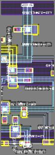
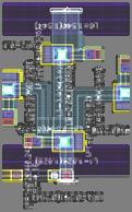
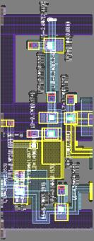
18 Chip Photograph of Half-Precision FPA Normalizer 1mm Shifter of A Half precision FPA Minimum interval: 12 clocks ( n f + 1) Latency: 23 clocks ( 2n f + 1) Operating frequency: 20 GHz Performance : GFLOPs # of JJs : JJs Power consumption : 3.5 mw Size : mm 2 Shifter Register of Significands Clock Generator Shifter Register of Exponent and Sign Controller Shifter of B Shifter Register for Confirmation *n f : bit length of significand Adder & Subtractor Normalize r Confirmation Shift ter Register for *SRL Nb 2.5 ka/cm 2 standard process CONNECT cooperated with SRL, NiCT, NU & YNU
19 DC Bias Margin of Each Component -10% -5% 0% 5% 10% 15% 20% 25% 30% 35% 40% Shifter_A Shifter_B Adder Normalizer of significand Normalizer of exponent Controller of shifter Controller of shifter and adder
 S F 2 E S: Sign E:")


20 Floating-Point Multiplier (-1) S F 2 E S: Sign E: Exponent F: Fraction Significand part is calculated by a systolic-array multiplier. S(1bit) E(8 bit) F(23 bit) Z f =XX f YY f Exponent part is calculated by a bit-serial adder. Z e =X e +Y e
.")
 MSB Input LSB")
21 Systolic-Array Multiplier - Composed of 1D array of 1-b processing element (PE). - Small hardware cost: (bit length) - High throughput : ~ 1/(bit length) MSB Input LSB MSB Output LSB


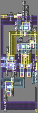
22 Chip Photograph of Half-Precision FPM Clock Generator Shifter Register Multiplier Normalizer Half precision FPM Minimum interval: 12 clocks ( n f + 1) Latency: 11 clocks (n f ) Operating frequency: 25 GHz Performance : GFLOPs # of JJs : JJs Power consumption : 3.5 mw Size : mm 2 1mm Adder and Normalizer Shifter Register *SRL Nb 2.5 ka/cm 2 standard process *n f : bit length of significand CONNECT cooperated with SRL, NiCT, NU & YNU


")
 + (-2) + 1 =")


23 Test Result of LSB MSB FX : EX: FY: EY: (10) FXY: EXY: (-2) [Calculation of exponent part ] (10) + (-2) + 1 = 9 EX EY Carry from fraction part Correct operation was confirmed at high speed. Maximum operating frequency: 31.5 GHz
 12 ( nf + 1) Latency (clocks) 23 (2 nf + 1) nf : bit length of fraction part FPA Clock Generator Normalizer Shifter Register")

24 Summary of Half-Precision FPUs Floating Point Adder Floating Point Multiplier # of JJs Size (mm2) 6.76 x x 3.78 Minimum interval (clocks) 12 ( nf + 1) Latency (clocks) 23 (2 nf + 1) nf : bit length of fraction part FPA Clock Generator Normalizer Shifter Register of Significands Adder & Subtractor Controller Norm alizer Clock Generator Shifter Register of Exponent and Sign Shifter of B 1mm Shift fter Register for Confirrmation Shifter of A Multiplier Shifter Register FPM Normalizer Normalizer Shifter Register 1mm Shifter Register for Confirmation CONNECT cooperated with SRL, NiCT, NU & YNU
25 NDRO-based and crossbar-based architectures of ORN ORN requirements: 1-to-N connections where N is an odd number connections to either input of the FPU FPU FPU FPU NDRO NDRO NDRO NDRO NDRO NDRO FPU FPU FPU M-FPUs + : small number of Josephson junctions required : irregular non-pipelined structure => with the increase of the complexity becomes cumbersome FPU FPU FPU ½CBT ½CBT ½CBT CBT CBT CBT CBT CBT CBT CBT FPU FPU FPU + : scalable pipelined easily re-designed for any number of N and M : large number of Josephson junctions required
26 Comparison of the ORN architectures NDRO-based ORN ORN complexity latency, ps skew, ps minimum interval number of control lines bias current, A power, mw number of JJ N=3, N M=8 M ~60 ~60 n f +60ps ~5500 N=5, M=10 ~80 ~80 n f +80ps ~8000 N=9, M=32 ~100 ~100 n f +100ps ~50500 Number of JJs of NDRO-based ORN in a table is an estimation based on a design of the switch for RDP prototype (N=3, M=4) that consisted of 2750 JJs and requires 300 ma bias current (Iwasaki, not published yet) Crossbar-based ORN ORN latency, skew, ps minimum number of bias power, number of complexity clocks interval control lines current, A mw JJ N=3, M=8 6 ~300 n f N=5, M=10 10 ~500 n f N=9, M=32 18 ~900 n f A crossbar switch with broadcasting function: 296 JJs Note that almost the same number of JJs are required for both ORNs if isometric (equal length wirings) network is employed in the NDRO-based ORN.


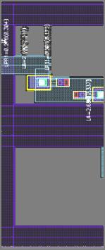
27 1 t 2 ORN test 1-to-2 t t dout01 dout11 dout12 dout02 dout11 dout01 bias_kern1 ladder clkin_lffin clkin hf clkin_hf din1 CBT1 CBT0 CBT2 clkout2 clkout1 clkout bar02 bar12 cross11 cross01 cross10 bar00 clkin_lfin lki lfi din0 clkin_lfout1 clkin lfo t1 clkin_lfout2 din2 bias_kern2 din0 bias_kern0 dout02 Example of the low frequency test: din0 -> dout01, dout02, dout12 dout12 Frequency dependence of the bias margins: din0 -> dout11 bias_kern1 margins for din0 -> dout11 routing CBT to-2 ORN: 2043 JJs, bias current 226 ma CBT0 Total test circuit: 3098 JJs Total bias current: 359 ma Example: open466, no. 4 chip F CBT completely functional, exhaustive test bias_kern0 = -14.6/5.3 % does not depend on the pattern bias_kern1 = -16.1/18.3 % for din0 -> dout11, dout12 bias_kern2 = -20.7/12.6 % for din0 -> dout11, dout12 minimum! bias_kern1 = -40.3/17.2% for din1 -> dout01 bias_kern2 = -38/12.6% for din2 -> dout02, dout12 maximum! upper margin lower margin
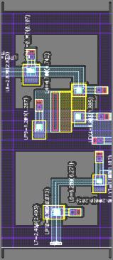
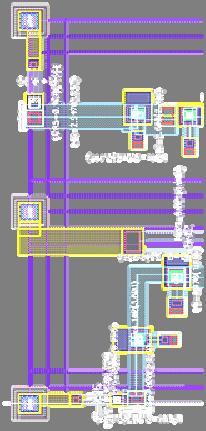
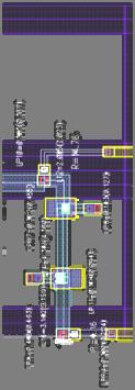
28 Design of 2x2 SFQ-RDP 11 pipeline stages Bias current: 1.27 A Designed frequency: 25 GHz Circuit area: 5.90 x 3.68 mm 2 InSR & OutSR length: 16-bits JJs Data length: 7-bits 1 mm Buffer Output SR Buffer Input SR ALU ORN ALU Controller


29 Demonstration of 2x2 SFQ-RDP Frequency characteristicof ti RDP Input patterns Output patterns Maximum operating frequency 23 GHz The function for each ALU is chosen as shown above.


30 Device Structure of Nb 10-layer Fabrication Process Active layer Including JJ and R Main GP and CPL 2 nd PTL layer 1 st PTL layer DC Power layer Bias pillar Bias pillar 10 ka/cm 2 Nb process


31 Layout DCP (M1) Bias Pillar (C1, 2, 3, 4, 5, 6, GC) 5 x 5 m 2 6 layers Moat (M2, 3, 4, 5, 6, 7) PTL (M3, 5) Width: m Via of PTLs less then 12 x 12 m 2 30 m Maximum current value: 2.4 ma (limited by size of contacts)


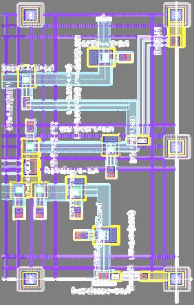

32 Cell library Jc: 10 ka/cm2 c = 2 D2FF CBE 30μm DC/SFQ SFQ/DC DFF JAND 30μm JANDF JNOR RTFFB JNOT SPL3 T1 JOR SPLL

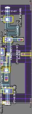
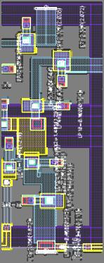
33 Design of Bit-Serial Half Adder using a New Cell Library Logic simulation results of bit-serial half adder J : 10 ka/cm 2 J c : 10 ka/cm c = 2


34 On-Chip High-Speed Test Results of Bit-Serial Half Adder Clock Generator Shift Register for Input Bit-Serial Shift Register for Output Adder J c : 10 ka/cm 2 c c = 2


35 Road Map of RSFQ LSRDP Processor 40 ka/cm 2 Process 10 TFLOPS LSRDP system development 100 GHz FPU & LSRDP prototype 10 ka/cm 2 Process 2.5 ka/cm 2 Process 25GHz FPU/RDP 60 GHz FPU & LSRDP prototype FPA Shifter Register of Significan Clock ds Generator Shifter Register of Exponent and Sign Normalizer Shifter of A Controller Shifter of B N Add o er r & m Sub a tract l or i z e r Shifter Register for Confirmation Shifter Register for Confirmation
36 Summary Our target is to make a fundamental technology for high-end supercomputers based on large-scale reconfigurable data-path (LRDP) architecture. Some key components were designed and implemented using standard Nb process, and their correct operations were demonstrated. Half-precision RSFQ FPA and FPU Operand routing network (ORN) 2 x 2 RDP Structure of the SRL advanced II process was determined and a new cell library is under development. 85 GHz operation of bit-serial half-adder was demonstrated.
Direct measurements of propagation delay of single-flux-quantum circuits by time-to-digital converters
 Direct measurements of propagation delay of single-flux-quantum circuits by time-to-digital converters Kazunori Nakamiya 1a), Nobuyuki Yoshikawa 1, Akira Fujimaki 2, Hirotaka Terai 3, and Yoshihito Hashimoto
2 SQUID. (Superconductive QUantum Interference Device) SQUID 2. ( 0 = Wb) SQUID SQUID SQUID SQUID Wb ( ) SQUID SQUID SQUID
 SQUID 2. ( 0 = Wb) SQUID SQUID SQUID SQUID Wb ( ) SQUID SQUID SQUID") SQUID (Superconductive QUantum Interference Device) SQUID ( 0 = 2.07 10-15 Wb) SQUID SQUID SQUID SQUID 10-20 Wb (10-5 0 ) SQUID SQUID ( 0 ) SQUID 0 [1, 2] SQUID 0.1 0 SQUID SQUID 10-4 0 1 1 1 SQUID 2 SQUID
SQUID (Superconductive QUantum Interference Device) SQUID ( 0 = 2.07 10-15 Wb) SQUID SQUID SQUID SQUID 10-20 Wb (10-5 0 ) SQUID SQUID ( 0 ) SQUID 0 [1, 2] SQUID 0.1 0 SQUID SQUID 10-4 0 1 1 1 SQUID 2 SQUID
Design and Operation Of Parallel Carry-Save Pipelined Rsfq Multiplier For Digital Signal Processing
 International Journal of Engineering Science Invention ISSN (Online): 2319 6734, ISSN (Print): 2319 6726 PP.35-40 Design and Operation Of Parallel Carry-Save Pipelined Rsfq Multiplier For Digital Signal
Design of 8-Bit RSFQ Based Multiplier for DSP Application
 International Journal of Innovative Research in Electronics and Communications (IJIREC) Volume 2, Issue 1, January 2015, PP 8-14 ISSN 2349-4042 (Print) & ISSN 2349-4050 (Online) www.arcjournals.org Design
Circuit Description and Design Flow of Superconducting SFQ Logic Circuits
 IEICE TRANS. ELECTRON., VOL.E97 C, NO.3 MARCH 2014 149 INVITED PAPER Special Section on Leading-Edge Technology of Superconductor Large-Scale Integrated Circuits Circuit Description and Design Flow of
IN the past few years, superconductor-based logic families
 1 Synthesis Flow for Cell-Based Adiabatic Quantum-Flux-Parametron Structural Circuit Generation with HDL Backend Verification Qiuyun Xu, Christopher L. Ayala, Member, IEEE, Naoki Takeuchi, Member, IEEE,
Advancement of superconductor digital electronics
 REVIEW PAPER IEICE Electronics Express, Vol.9, No.22, 1720 1734 Advancement of superconductor digital electronics Akira Fujimaki a) Department of Quantum Engineering, Nagoya University Furo-cho, Chikusa-ku,
SINGLE FLUX QUANTUM ONE-DECIMAL-DIGIT RNS ADDER
 Applied Superconductivity Vol. 6, Nos 10±12, pp. 609±614, 1998 # 1999 Published by Elsevier Science Ltd. All rights reserved Printed in Great Britain PII: S0964-1807(99)00018-6 0964-1807/99 $ - see front
FPGA IMPLEMENTATION OF 32-BIT WAVE-PIPELINED SPARSE- TREE ADDER
 FPGA IMPLEMENTATION OF 32-BIT WAVE-PIPELINED SPARSE- TREE ADDER Kasharaboina Thrisandhya *1, LathaSahukar *2 1 Post graduate (M.Tech) in ATRI, JNTUH University, Telangana, India. 2 Associate Professor
Low Temperature Superconductor Electronics. H.-G. Meyer, Institute of Photonic Technology Albert Einstein Strasse Jena, Germany
 1 Low Temperature Superconductor Electronics H.-G. Meyer, Institute of Photonic Technology Albert Einstein Strasse 9 07745 Jena, Germany 2 Outline Status of Semiconductor Technology Introduction to Superconductor
DIGIT SERIAL PROCESSING ELEMENTS. Bit-Serial Multiplication. Digit-serial arithmetic processes one digit of size d in each time step.
 IGIT SERIAL PROCESSING ELEMENTS 1 BIT-SERIAL ARITHMETIC 2 igit-serial arithmetic processes one digit of size d in each time step. if d = W d => conventional bit-parallel arithmetic if d = 1 => bit-serial
Superconducting Digital Signal Processor for Telecommunication
 Superconducting Digital Signal Processor for Telecommunication Anna Herr Microtechnology and Nanoscience, Chalmers University of Technology 41296 Gothenburg, Sweden e-mail: anna.herr@chalmers.se Abstract-
High performance Radix-16 Booth Partial Product Generator for 64-bit Binary Multipliers
 High performance Radix-16 Booth Partial Product Generator for 64-bit Binary Multipliers Dharmapuri Ranga Rajini 1 M.Ramana Reddy 2 rangarajini.d@gmail.com 1 ramanareddy055@gmail.com 2 1 PG Scholar, Dept
Design and demonstration of a 5-bit flash-type SFQ A/D converter integrated with error correction and interleaving circuits
 & ESAS European Superconductivity News Forum (ESNF), No. 14, October 21 The published version of this manuscript appeared in IEEE Transactions on Applied Superconductivity 21, Issue 3, 671-676 (211) 2EB-1,
IEEE TRANSACTIONS ON APPLIED SUPERCONDUCTIVITY, VOL. 28, NO. 2, MARCH
 IEEE TRANSACTIONS ON APPLIED SUPERCONDUCTIVITY, VOL. 28, NO. 2, MARCH 2018 1300212 Superconducting Magnetic Field Programmable Gate Array Naveen Kumar Katam, Oleg A. Mukhanov, Fellow, IEEE, and Massoud
Lecture 3: Logic circuit. Combinational circuit and sequential circuit
 Lecture 3: Logic circuit Combinational circuit and sequential circuit TRAN THI HONG HONG@IS.NAIST.JP Content Lecture : Computer organization and performance evaluation metrics Lecture 2: Processor architecture
JDT LOW POWER FIR FILTER ARCHITECTURE USING ACCUMULATOR BASED RADIX-2 MULTIPLIER
 JDT-003-2013 LOW POWER FIR FILTER ARCHITECTURE USING ACCUMULATOR BASED RADIX-2 MULTIPLIER 1 Geetha.R, II M Tech, 2 Mrs.P.Thamarai, 3 Dr.T.V.Kirankumar 1 Dept of ECE, Bharath Institute of Science and Technology
Digital Integrated CircuitDesign
 Digital Integrated CircuitDesign Lecture 13 Building Blocks (Multipliers) Register Adder Shift Register Adib Abrishamifar EE Department IUST Acknowledgement This lecture note has been summarized and categorized
Multi-Channel Time Digitizing Systems
 454 IEEE TRANSACTIONS ON APPLIED SUPERCONDUCTIVITY, VOL. 13, NO. 2, JUNE 2003 Multi-Channel Time Digitizing Systems Alex Kirichenko, Saad Sarwana, Deep Gupta, Irwin Rochwarger, and Oleg Mukhanov Abstract
Technology Timeline. Transistors ICs (General) SRAMs & DRAMs Microprocessors SPLDs CPLDs ASICs. FPGAs. The Design Warrior s Guide to.
 SRAMs & DRAMs Microprocessors SPLDs CPLDs ASICs. FPGAs. The Design Warrior s Guide to.") FPGAs 1 CMPE 415 Technology Timeline 1945 1950 1955 1960 1965 1970 1975 1980 1985 1990 1995 2000 Transistors ICs (General) SRAMs & DRAMs Microprocessors SPLDs CPLDs ASICs FPGAs The Design Warrior s Guide
FPGAs 1 CMPE 415 Technology Timeline 1945 1950 1955 1960 1965 1970 1975 1980 1985 1990 1995 2000 Transistors ICs (General) SRAMs & DRAMs Microprocessors SPLDs CPLDs ASICs FPGAs The Design Warrior s Guide
CHAPTER 5 DESIGN OF COMBINATIONAL LOGIC CIRCUITS IN QCA
 90 CHAPTER 5 DESIGN OF COMBINATIONAL LOGIC CIRCUITS IN QCA 5.1 INTRODUCTION A combinational circuit consists of logic gates whose outputs at any time are determined directly from the present combination
Comparator Design Analysis using Efficient Low Power Full Adder Meena Aggarwal 1, Rajesh Mehra 2 1 ME student (ECE), 2 Associate Professor
, 2 Associate Professor") International Journal of Engineering Trends and Technology (IJETT) olume 26 Number 1- August 2015 Comparator Design Analysis using Efficient Low Power Full Adder Meena Aggarwal 1, Rajesh Mehra 2 1 ME student
International Journal of Engineering Trends and Technology (IJETT) olume 26 Number 1- August 2015 Comparator Design Analysis using Efficient Low Power Full Adder Meena Aggarwal 1, Rajesh Mehra 2 1 ME student
High-Speed RSA Crypto-Processor with Radix-4 4 Modular Multiplication and Chinese Remainder Theorem
 High-Speed RSA Crypto-Processor with Radix-4 4 Modular Multiplication and Chinese Remainder Theorem Bonseok Koo 1, Dongwook Lee 1, Gwonho Ryu 1, Taejoo Chang 1 and Sangjin Lee 2 1 Nat (NSRI), Korea 2 Center
Design and Implementation of Single Bit ALU Using PTL & GDI Technique
 Volume 5 Issue 1 March 2017 ISSN: 2320-9984 (Online) International Journal of Modern Engineering & Management Research Website: www.ijmemr.org Design and Implementation of Single Bit ALU Using PTL & GDI
IMPLEMENTING THE 10-BIT, 50MS/SEC PIPELINED ADC
 98 CHAPTER 5 IMPLEMENTING THE 0-BIT, 50MS/SEC PIPELINED ADC 99 5.0 INTRODUCTION This chapter is devoted to describe the implementation of a 0-bit, 50MS/sec pipelined ADC with different stage resolutions
THE Josephson junction based digital superconducting
 IEEE TRANSACTIONS ON APPLIED SUPERCONDUCTIVITY, VOL. 26, NO. 3, APRIL 2016 1300205 Investigation of Readout Cell Configuration and Parameters on Functionality and Stability of Bi-Directional RSFQ TFF Tahereh
Design of 64-Bit Low Power ALU for DSP Applications
 Design of 64-Bit Low Power ALU for DSP Applications J. Nandini 1, V.V.M.Krishna 2 1 M.Tech Scholar [VLSI Design], Department of ECE, KECW, Narasaraopet, A.P., India 2 Associate Professor, Department of
A New network multiplier using modified high order encoder and optimized hybrid adder in CMOS technology
 Inf. Sci. Lett. 2, No. 3, 159-164 (2013) 159 Information Sciences Letters An International Journal http://dx.doi.org/10.12785/isl/020305 A New network multiplier using modified high order encoder and optimized
AREA EFFICIENT DISTRIBUTED ARITHMETIC DISCRETE COSINE TRANSFORM USING MODIFIED WALLACE TREE MULTIPLIER
 American Journal of Applied Sciences 11 (2): 180-188, 2014 ISSN: 1546-9239 2014 Science Publication doi:10.3844/ajassp.2014.180.188 Published Online 11 (2) 2014 (http://www.thescipub.com/ajas.toc) AREA
DIGITAL INTEGRATED CIRCUITS A DESIGN PERSPECTIVE 2 N D E D I T I O N
 DIGITAL INTEGRATED CIRCUITS A DESIGN PERSPECTIVE 2 N D E D I T I O N Jan M. Rabaey, Anantha Chandrakasan, and Borivoje Nikolic CONTENTS PART I: THE FABRICS Chapter 1: Introduction (32 pages) 1.1 A Historical
A Prescaler Circuit for a Superconductive Time-to-Digital Converter
 IEEE TRANSACTIONS ON APPLIED SUPERCONDUCTIVITY, VOL. 11, No. 1, MARCH 2001 513 A Prescaler Circuit for a Superconductive Time-to-Digital Converter Steven B. Kaplan, Alex F. Kirichenko, Oleg A. Mukhanov,
Analyzing Metrics of ALU Designs Traversing from Years 2002 to 2015
 Analyzing Metrics of ALU Designs Traversing from Years 2002 to 2015 Brianna V. Thomason Department of Electrical and Computer Engineering University of Central Flida Orlando, FL 32816-2362 Email: brianna.thomason@knights.ucf.edu
SIGNED PIPELINED MULTIPLIER USING HIGH SPEED COMPRESSORS
 INTERNATIONAL JOURNAL OF RESEARCH IN COMPUTER APPLICATIONS AND ROBOTICS ISSN 2320-7345 SIGNED PIPELINED MULTIPLIER USING HIGH SPEED COMPRESSORS 1 T.Thomas Leonid, 2 M.Mary Grace Neela, and 3 Jose Anand
Design of Baugh Wooley Multiplier with Adaptive Hold Logic. M.Kavia, V.Meenakshi
 International Journal of Scientific & Engineering Research, Volume 6, Issue 4, April-2015 105 Design of Baugh Wooley Multiplier with Adaptive Hold Logic M.Kavia, V.Meenakshi Abstract Mostly, the overall
A Superconductive Flash Digitizer with On-Chip Memory
 32 IEEE TRANSACTIONS ON APPLIED SUPERCONDUCTIVITY, VOL. 9, No. 2, JUNE 1999 A Superconductive Flash Digitizer with On-Chip Memory Steven B. Kaplan, Paul D. Bradley*, Darren K. Brock, Dmitri Gaidarenko,
Vector Arithmetic Logic Unit Amit Kumar Dutta JIS College of Engineering, Kalyani, WB, India
 Vol. 2 Issue 2, December -23, pp: (75-8), Available online at: www.erpublications.com Vector Arithmetic Logic Unit Amit Kumar Dutta JIS College of Engineering, Kalyani, WB, India Abstract: Real time operation
Design & Analysis of Low Power Full Adder
 1174 Design & Analysis of Low Power Full Adder Sana Fazal 1, Mohd Ahmer 2 1 Electronics & communication Engineering Integral University, Lucknow 2 Electronics & communication Engineering Integral University,
Digital Encoder for RF Transmit Waveform Synthesizer Amol Inamdar, Deepnarayan Gupta, Saad Sarwana, Anubhav Sahu, and Alan M.
 556 IEEE TRANSACTIONS ON APPLIED SUPERCONDUCTIVITY, VOL. 17, NO. 2, JUNE 2007 Digital Encoder for RF Transmit Waveform Synthesizer Amol Inamdar, Deepnarayan Gupta, Saad Sarwana, Anubhav Sahu, and Alan
Serial Parallel Multiplier Design in Quantum-dot Cellular Automata
 Serial Parallel ultiplier Design in Quantum-dot Cellular Automata Heumpil Cho Qualcomm, Inc. 5775 orehouse Dr. San Diego, California 92121 Email: hpcho@qualcomm.com Earl E. Swartzlander, Jr. Department
EECS150 - Digital Design Lecture 23 - Arithmetic and Logic Circuits Part 4. Outline
 EECS150 - Digital Design Lecture 23 - Arithmetic and Logic Circuits Part 4 April 19, 2005 John Wawrzynek Spring 2005 EECS150 - Lec23-alc4 Page 1 Outline Shifters / Rotators Fixed shift amount Variable
HIGH PERFORMANCE BAUGH WOOLEY MULTIPLIER USING CARRY SKIP ADDER STRUCTURE
 HIGH PERFORMANCE BAUGH WOOLEY MULTIPLIER USING CARRY SKIP ADDER STRUCTURE R.ARUN SEKAR 1 B.GOPINATH 2 1Department Of Electronics And Communication Engineering, Assistant Professor, SNS College Of Technology,
Sno Projects List IEEE. High - Throughput Finite Field Multipliers Using Redundant Basis For FPGA And ASIC Implementations
 Sno Projects List IEEE 1 High - Throughput Finite Field Multipliers Using Redundant Basis For FPGA And ASIC Implementations 2 A Generalized Algorithm And Reconfigurable Architecture For Efficient And Scalable
ASIC Implementation of High Speed Area Efficient Arithmetic Unit using GDI based Vedic Multiplier
 INTERNATIONAL JOURNAL OF APPLIED RESEARCH AND TECHNOLOGY ISSN 2519-5115 RESEARCH ARTICLE ASIC Implementation of High Speed Area Efficient Arithmetic Unit using GDI based Vedic Multiplier 1 M. Sangeetha
Course Outcome of M.Tech (VLSI Design)
") Course Outcome of M.Tech (VLSI Design) PVL108: Device Physics and Technology The students are able to: 1. Understand the basic physics of semiconductor devices and the basics theory of PN junction. 2.
Course Outcome of M.Tech (VLSI Design) PVL108: Device Physics and Technology The students are able to: 1. Understand the basic physics of semiconductor devices and the basics theory of PN junction. 2.
EE247 Lecture 22. Figures of merit (FOM) and trends for ADCs How to use/not use FOM. EECS 247 Lecture 22: Data Converters 2004 H. K.
 and trends for ADCs How to use/not use FOM. EECS 247 Lecture 22: Data Converters 2004 H. K.") EE247 Lecture 22 Pipelined ADCs Combining the bits Stage implementation Circuits Noise budgeting Figures of merit (FOM) and trends for ADCs How to use/not use FOM Oversampled ADCs EECS 247 Lecture 22:
EE247 Lecture 22 Pipelined ADCs Combining the bits Stage implementation Circuits Noise budgeting Figures of merit (FOM) and trends for ADCs How to use/not use FOM Oversampled ADCs EECS 247 Lecture 22:
A new 6-T multiplexer based full-adder for low power and leakage current optimization
 A new 6-T multiplexer based full-adder for low power and leakage current optimization G. Ramana Murthy a), C. Senthilpari, P. Velrajkumar, and T. S. Lim Faculty of Engineering and Technology, Multimedia
Design and Analysis of Row Bypass Multiplier using various logic Full Adders
 Design and Analysis of Row Bypass Multiplier using various logic Full Adders Dr.R.Naveen 1, S.A.Sivakumar 2, K.U.Abhinaya 3, N.Akilandeeswari 4, S.Anushya 5, M.A.Asuvanti 6 1 Associate Professor, 2 Assistant
EECS150 - Digital Design Lecture 28 Course Wrap Up. Recap 1
 EECS150 - Digital Design Lecture 28 Course Wrap Up Dec. 5, 2013 Prof. Ronald Fearing Electrical Engineering and Computer Sciences University of California, Berkeley (slides courtesy of Prof. John Wawrzynek)
An Optimized Wallace Tree Multiplier using Parallel Prefix Han-Carlson Adder for DSP Processors
 An Optimized Wallace Tree Multiplier using Parallel Prefix Han-Carlson Adder for DSP Processors T.N.Priyatharshne Prof. L. Raja, M.E, (Ph.D) A. Vinodhini ME VLSI DESIGN Professor, ECE DEPT ME VLSI DESIGN
Superconducting Technology Assessment. Position Papers
 Superconducting Technology Assessment Position Papers Contents: Towards a Technology and Architecture Hybrid? o Thomas Sterling, Panel Moderator Superconductor Technology for High-End Computing System
CHAPTER 1 INTRODUCTION
 CHAPTER 1 INTRODUCTION 1.1 Project Background High speed multiplication is another critical function in a range of very large scale integration (VLSI) applications. Multiplications are expensive and slow
CS 61C: Great Ideas in Computer Architecture Finite State Machines, Functional Units
 CS 61C: Great Ideas in Computer Architecture Finite State Machines, Functional Units Instructors: Vladimir Stojanovic and Nicholas Weaver http://inst.eecs.berkeley.edu/~cs61c/sp16 1 Machine Interpretation
The Metrics and Designs of an Arithmetic Logic Function over
 The Metrics and Designs of an Arithmetic Logic Function over 2002-2015 Jimmy Vallejo Department of Electrical and Computer Engineering University of Central Flida Orlando, FL 32816-2362 Abstract There
Another way to implement a folding ADC
 Another way to implement a folding ADC J. Van Valburg and R. van de Plassche, An 8-b 650 MHz Folding ADC, IEEE JSSC, vol 27, #12, pp. 1662-6, Dec 1992 Coupled Differential Pair J. Van Valburg and R. van
High Performance Low-Power Signed Multiplier
 High Performance Low-Power Signed Multiplier Amir R. Attarha Mehrdad Nourani VLSI Circuits & Systems Laboratory Department of Electrical and Computer Engineering University of Tehran, IRAN Email: attarha@khorshid.ece.ut.ac.ir
By Dayadi Lakshmaiah, Dr. M. V. Subramanyam & Dr. K. Satya Prasad Jawaharlal Nehru Technological University, India
 Global Journal of Researches in Engineering: F Electrical and Electronics Engineering Volume 14 Issue 9 Version 1.0 Type: Double Blind Peer Reviewed International Research Journal Publisher: Global Journals
A Study of The Advancement of CMOS ALU & Full Adder Circuit Design For Modern Design
 A Study of The Advancement of & Full Adder Circuit Design F Modern Design Bruce Hardy BR759875 Department of Electrical and Computer Engineering University of Central Flida Orlando, FL 32816-2362 Abstract
Energy-Efficient Single Flux Quantum Technology
 to appear in IEEE Trans. Appl. Supercond., vol. 21, no. 3, June 2011 (Invited talk at the ASC 2010, Washington, DC) 1 Energy-Efficient Single Flux Quantum Technology Oleg A. Mukhanov, Senior Member, IEEE
FPGA IMPLENTATION OF REVERSIBLE FLOATING POINT MULTIPLIER USING CSA
 FPGA IMPLENTATION OF REVERSIBLE FLOATING POINT MULTIPLIER USING CSA Vidya Devi M 1, Lakshmisagar H S 1 1 Assistant Professor, Department of Electronics and Communication BMS Institute of Technology,Bangalore
VLSI DESIGN OF DIGIT-SERIAL FPGA ARCHITECTURE
 Journal of Circuits, Systems, and Computers Vol. 3, No. (24) 7 52 c World Scientific Publishing Company VLSI ESIGN OF IGIT-SERIAL FPGA ARCHITECTURE HANHO LEE School of Information and Communication Engineering,
Area Efficient and Low Power Reconfiurable Fir Filter
 50 Area Efficient and Low Power Reconfiurable Fir Filter A. UMASANKAR N.VASUDEVAN N.Kirubanandasarathy Research scholar St.peter s university, ECE, Chennai- 600054, INDIA Dean (Engineering and Technology),
Low Power R4SDC Pipelined FFT Processor Architecture
 IOSR Journal of VLSI and Signal Processing (IOSR-JVSP) e-issn: 2319 4200, p-issn No. : 2319 4197 Volume 1, Issue 6 (Mar. Apr. 2013), PP 68-75 Low Power R4SDC Pipelined FFT Processor Architecture Anjana
REVIEW ARTICLE: EFFICIENT MULTIPLIER ARCHITECTURE IN VLSI DESIGN
 REVIEW ARTICLE: EFFICIENT MULTIPLIER ARCHITECTURE IN VLSI DESIGN M. JEEVITHA 1, R.MUTHAIAH 2, P.SWAMINATHAN 3 1 P.G. Scholar, School of Computing, SASTRA University, Tamilnadu, INDIA 2 Assoc. Prof., School
Low Power 8-Bit ALU Design Using Full Adder and Multiplexer
 Low Power 8-Bit ALU Design Using Full Adder and Multiplexer Gaddam Sushil Raj B.Tech, Vardhaman College of Engineering. ABSTRACT: Arithmetic logic unit (ALU) is an important part of microprocessor. In
Electronic Design Automation at Transistor Level by Ricardo Reis. Preamble
 1 Electronic Design Automation at Transistor Level by Ricardo Reis Preamble 1 Quintillion of Transistors 90 65 45 32 NM Electronic Design Automation at Transistor Level Ricardo Reis Universidade Federal
Mahendra Engineering College, Namakkal, Tamilnadu, India.
 Implementation of Modified Booth Algorithm for Parallel MAC Stephen 1, Ravikumar. M 2 1 PG Scholar, ME (VLSI DESIGN), 2 Assistant Professor, Department ECE Mahendra Engineering College, Namakkal, Tamilnadu,
A design of 16-bit adiabatic Microprocessor core
 194 A design of 16-bit adiabatic Microprocessor core Youngjoon Shin, Hanseung Lee, Yong Moon, and Chanho Lee Abstract A 16-bit adiabatic low-power Microprocessor core is designed. The processor consists
CMOS Process Variations: A Critical Operation Point Hypothesis
 CMOS Process Variations: A Critical Operation Point Hypothesis Janak H. Patel Department of Electrical and Computer Engineering University of Illinois at Urbana-Champaign jhpatel@uiuc.edu Computer Systems
A 10-Gb/s Multiphase Clock and Data Recovery Circuit with a Rotational Bang-Bang Phase Detector
 JOURNAL OF SEMICONDUCTOR TECHNOLOGY AND SCIENCE, VOL.16, NO.3, JUNE, 2016 ISSN(Print) 1598-1657 http://dx.doi.org/10.5573/jsts.2016.16.3.287 ISSN(Online) 2233-4866 A 10-Gb/s Multiphase Clock and Data Recovery
S.Nagaraj 1, R.Mallikarjuna Reddy 2
 FPGA Implementation of Modified Booth Multiplier S.Nagaraj, R.Mallikarjuna Reddy 2 Associate professor, Department of ECE, SVCET, Chittoor, nagarajsubramanyam@gmail.com 2 Associate professor, Department
Disseny físic. Disseny en Standard Cells. Enric Pastor Rosa M. Badia Ramon Canal DM Tardor DM, Tardor
 Disseny físic Disseny en Standard Cells Enric Pastor Rosa M. Badia Ramon Canal DM Tardor 2005 DM, Tardor 2005 1 Design domains (Gajski) Structural Processor, memory ALU, registers Cell Device, gate Transistor
<Explanation of Improved the Quality of ALU And Ten Different Types of Designs for Decreasing Power Dissipation>
 Jihang Li Department of Electrical and Computer Engineering University of Central Flida Orlando,
DESIGN OF PARALLEL MULTIPLIERS USING HIGH SPEED ADDER
 DESIGN OF PARALLEL MULTIPLIERS USING HIGH SPEED ADDER Mr. M. Prakash Mr. S. Karthick Ms. C Suba PG Scholar, Department of ECE, BannariAmman Institute of Technology, Sathyamangalam, T.N, India 1, 3 Assistant
12-Bit Pipeline ADC Implemented in 0.09-um Digital CMOS Technology for Powerline Alliance
 2-Bit Pipeline ADC Implemented in 0.09-um Digital CMOS Technology for Powerline Alliance Olga Joy L. Gerasta, Lavern S. Bete, Jayson C. Loreto, Sheerah Dale M. Orlasan, and Honey Mae N. Tagalogon Microelectronics
A Fixed-Width Modified Baugh-Wooley Multiplier Using Verilog
 A Fixed-Width Modified Baugh-Wooley Multiplier Using Verilog K.Durgarao, B.suresh, G.Sivakumar, M.Divaya manasa Abstract Digital technology has advanced such that there is an increased need for power efficient
International Journal of Scientific & Engineering Research Volume 3, Issue 12, December ISSN
 International Journal of Scientific & Engineering Research Volume 3, Issue 12, December-2012 1 Optimized Design and Implementation of an Iterative Logarithmic Signed Multiplier Sanjeev kumar Patel, Vinod
Design of Low power and Area Efficient 8-bit ALU using GDI Full Adder and Multiplexer
 Design of Low power and Area Efficient 8-bit ALU using GDI Full Adder and Multiplexer Mr. Y.Satish Kumar M.tech Student, Siddhartha Institute of Technology & Sciences. Mr. G.Srinivas, M.Tech Associate
Design of an Energy Efficient 4-2 Compressor
 IOP Conference Series: Materials Science and Engineering PAPER OPEN ACCESS Design of an Energy Efficient 4-2 Compressor To cite this article: Manish Kumar and Jonali Nath 2017 IOP Conf. Ser.: Mater. Sci.
Option 1: A programmable Digital (FIR) Filter
 Filter") Design Project Your design project is basically a module filter. A filter is basically a weighted sum of signals. The signals (input) may be related, e.g. a delayed versions of each other in time, e.g.
Design Project Your design project is basically a module filter. A filter is basically a weighted sum of signals. The signals (input) may be related, e.g. a delayed versions of each other in time, e.g.
Integrated Circuit Design 813 Stellenbosch University Dept. E&E Engineering
 ICD 813 Lecture 1 p.1 Integrated Circuit Design 813 Stellenbosch University Dept. E&E Engineering 2013 Course contents Lecture 1: GHz digital electronics: RSFQ logic family Introduction to fast digital
Interconnect-Power Dissipation in a Microprocessor
 4/2/2004 Interconnect-Power Dissipation in a Microprocessor N. Magen, A. Kolodny, U. Weiser, N. Shamir Intel corporation Technion - Israel Institute of Technology 4/2/2004 2 Interconnect-Power Definition
II. QUATERNARY CONVERTER CIRCUITS
 Application of Galois Field in VLSI Using Multi-Valued Logic Ankita.N.Sakhare 1, M.L.Keote 2 1 Dept of Electronics and Telecommunication, Y.C.C.E, Wanadongri, Nagpur, India 2 Dept of Electronics and Telecommunication,
Very Large Scale Integration (VLSI)
") Very Large Scale Integration (VLSI) Lecture 6 Dr. Ahmed H. Madian Ah_madian@hotmail.com Dr. Ahmed H. Madian-VLSI 1 Contents Array subsystems Gate arrays technology Sea-of-gates Standard cell Macrocell
Very Large Scale Integration (VLSI) Lecture 6 Dr. Ahmed H. Madian Ah_madian@hotmail.com Dr. Ahmed H. Madian-VLSI 1 Contents Array subsystems Gate arrays technology Sea-of-gates Standard cell Macrocell
Low-Power VLSI. Seong-Ook Jung VLSI SYSTEM LAB, YONSEI University School of Electrical & Electronic Engineering
 Low-Power VLSI Seong-Ook Jung 2013. 5. 27. sjung@yonsei.ac.kr VLSI SYSTEM LAB, YONSEI University School of Electrical & Electronic Engineering Contents 1. Introduction 2. Power classification & Power performance
Low-Power Multipliers with Data Wordlength Reduction
 Low-Power Multipliers with Data Wordlength Reduction Kyungtae Han, Brian L. Evans, and Earl E. Swartzlander, Jr. Dept. of Electrical and Computer Engineering The University of Texas at Austin Austin, TX
COMPARISION OF LOW POWER AND DELAY USING BAUGH WOOLEY AND WALLACE TREE MULTIPLIERS
 COMPARISION OF LOW POWER AND DELAY USING BAUGH WOOLEY AND WALLACE TREE MULTIPLIERS ( 1 Dr.V.Malleswara rao, 2 K.V.Ganesh, 3 P.Pavan Kumar) 1 Professor &HOD of ECE,GITAM University,Visakhapatnam. 2 Ph.D
EE241 - Spring 2004 Advanced Digital Integrated Circuits. Announcements. Borivoje Nikolic. Lecture 15 Low-Power Design: Supply Voltage Scaling
 EE241 - Spring 2004 Advanced Digital Integrated Circuits Borivoje Nikolic Lecture 15 Low-Power Design: Supply Voltage Scaling Announcements Homework #2 due today Midterm project reports due next Thursday
A Novel Approach For Designing A Low Power Parallel Prefix Adders
 A Novel Approach For Designing A Low Power Parallel Prefix Adders R.Chaitanyakumar M Tech student, Pragati Engineering College, Surampalem (A.P, IND). P.Sunitha Assistant Professor, Dept.of ECE Pragati
A Static Power Model for Architects
 A Static Power Model for Architects J. Adam Butts and Guri Sohi University of Wisconsin-Madison {butts,sohi}@cs.wisc.edu 33rd International Symposium on Microarchitecture Monterey, California December,
Architectures and circuits for timeinterleaved. Sandeep Gupta Teranetics, Santa Clara, CA
 Architectures and circuits for timeinterleaved ADC s Sandeep Gupta Teranetics, Santa Clara, CA Outline Introduction to time-interleaved architectures. Conventional Sampling architectures and their application
Sophisticated design of low power high speed full adder by using SR-CPL and Transmission Gate logic
 Scientific Journal of Impact Factor(SJIF): 3.134 International Journal of Advance Engineering and Research Development Volume 2,Issue 3, March -2015 e-issn(o): 2348-4470 p-issn(p): 2348-6406 Sophisticated
Modified Booth Encoding Multiplier for both Signed and Unsigned Radix Based Multi-Modulus Multiplier
 Modified Booth Encoding Multiplier for both Signed and Unsigned Radix Based Multi-Modulus Multiplier M.Shiva Krushna M.Tech, VLSI Design, Holy Mary Institute of Technology And Science, Hyderabad, T.S,
Fault Tolerance in VLSI Systems
 Fault Tolerance in VLSI Systems Overview Opportunities presented by VLSI Problems presented by VLSI Redundancy techniques in VLSI design environment Duplication with complementary logic Self-checking logic
A Low-Power High-speed Pipelined Accumulator Design Using CMOS Logic for DSP Applications
 International Journal of Research Studies in Computer Science and Engineering (IJRSCSE) Volume. 1, Issue 5, September 2014, PP 30-42 ISSN 2349-4840 (Print) & ISSN 2349-4859 (Online) www.arcjournals.org
A New High Speed Low Power Performance of 8- Bit Parallel Multiplier-Accumulator Using Modified Radix-2 Booth Encoded Algorithm
 A New High Speed Low Power Performance of 8- Bit Parallel Multiplier-Accumulator Using Modified Radix-2 Booth Encoded Algorithm V.Sandeep Kumar Assistant Professor, Indur Institute Of Engineering & Technology,Siddipet
UNIT-II LOW POWER VLSI DESIGN APPROACHES
 UNIT-II LOW POWER VLSI DESIGN APPROACHES Low power Design through Voltage Scaling: The switching power dissipation in CMOS digital integrated circuits is a strong function of the power supply voltage.
Full-gate verification of superconducting integrated circuit layouts with InductEx
 1 Full-gate verification of superconducting integrated circuit layouts with InductEx Coenrad J. Fourie, Member, IEEE Abstract At present, superconducting integrated circuit layouts are verified through
REALIZATION OF FPGA BASED Q-FORMAT ARITHMETIC LOGIC UNIT FOR POWER ELECTRONIC CONVERTER APPLICATIONS
 17 Chapter 2 REALIZATION OF FPGA BASED Q-FORMAT ARITHMETIC LOGIC UNIT FOR POWER ELECTRONIC CONVERTER APPLICATIONS In this chapter, analysis of FPGA resource utilization using QALU, and is compared with
CARRY SAVE COMMON MULTIPLICAND MONTGOMERY FOR RSA CRYPTOSYSTEM
 American Journal of Applied Sciences 11 (5): 851-856, 2014 ISSN: 1546-9239 2014 Science Publication doi:10.3844/ajassp.2014.851.856 Published Online 11 (5) 2014 (http://www.thescipub.com/ajas.toc) CARRY
High Performance 128 Bits Multiplexer Based MBE Multiplier for Signed-Unsigned Number Operating at 1GHz
 High Performance 128 Bits Multiplexer Based MBE Multiplier for Signed-Unsigned Number Operating at 1GHz Ravindra P Rajput Department of Electronics and Communication Engineering JSS Research Foundation,