Integrated On-Chip Inductors using Magnetic Films Donald S. Gardner, Gerhard Schrom,
|
|
|
- Beverly Matthews
- 5 years ago
- Views:
Transcription
1 Integrated On-Chip Inductors using Magnetic Films Donald S. Gardner, Gerhard Schrom, Fabrice Paillet, Tanay Karnik, Shekhar Borkar, Circuits Research Lab & Future Technology Research Intel Labs Intel Corporation
2 Outline Magnetic material properties Magnetic hysteresis loops Complex permeability spectra Magnetic anisotropy Inductor measurements Structure cross sections Inductance measurements Sheet and shunt inductance Measurement analysis and modeling Eddy current and skin effect Time constant and Quality factor Effectiveness of laminations
3 RF CMOS Integrated Circuit Inductors make up 24% of this chip Inductance density of spirals is small (<100 nh/mm 2 )
4 100~480 MHz Switching Regulator V IN =1.2V, V OUT =0.9V, L=6.8nH, F=233MHz Φ 3 Φ 2 Discrete Φ 1 Inductors Φ 0 4.3ns High frequency Hysteretic multi-phase topology 1ns response 88% efficiency Schrom, Gardner, et.al., IEEE PESC 2004 and IEEE VLSI Symp
5 Comparison of DC Converters [3] [4] [5] [6] [7] Pavo-1 Year Tech [µm] n/a 0.25 n/a 0.25 n/a 0.09 # phases V IN [V] V OUT [V] f [MHz] Eff. [%] L TOT [µh] C [µf] n/a n/a I MAX [A] x higher f 1000x Smaller L and C Area [mm 2 ] n/a n/a 0.14
6 Inductor Test Chips Circa 1997~2000 Circa 2001~2005 Circa 2005~2008 Thin Aluminum Thin CoZrTa GHz response demonstrated Thick Aluminum Thick CoZrTa High inductance demonstration Thick Cu/Polyimide Thick Lam. CoZrTa High Q inductors demonstrated
7 Peak Qu uality Factor Inductance Densities vs. Q-Factor Song 2001 from the Literature Fukuda 2003 Saleh 1970 Orlando 2006 O'Donnell 2008 Viala 2004 Gardner 2007 Lee 2008 Yamaguchi 1991 Yachi 1991 Yamaguchi Kim 1997 Ahn 1994 Planar Spiral Gardner 2006 Elongated Spiral Stripline Toroidal Meander Liakopoulos 1999 Gardner Inductance Density (nh/mm 2 ) Gardner, Jamieson, et.al. IEEE Trans. Magnetics, 45, pp. 4760, 2009.
8 Flux Density B (T) Magnetic Hystersis Loops for CoZrTa Hard axis Easy axis Slope µ = Applied Magnetic Field H (Oe) Coercivity < 0.02 Oe minimizing hysteretic losses.
9 Permeability vs. Applied Magnetic Field Permea ability (Gauss/Oe) µm 1.5 µm 1.5 µm, 3 lams 4 µm 10 µm Applied Magnetic Field Bias (Oe) 20 Magnetic anisotropy H k has two components: The intrinsic induced anisotropy from the deposition The demagnetizing energy caused by the sample shape
10 Complex Permeability Model δ = 2ρ ωµ i µ o δ = skin depth ρ = resistivity of magnetic film ω = frequency µ i = relative dc permeability d = film thickness Skin depth (µm m) µm CoZrTa 4 µm CoZrTa 2 µm CoZrTa 0.5 µm CoZrTa Frequency (MHz) µ = 2 δ (1 + j ) d µ i tanh (1 + j) d 2δ High resistivity materials are needed to reduce the eddy currents and increase the skin depth. CoZrTa ρ = 100 µω-cm
11 Permeability Spectra of CoZrTa Real Component Imaginary Component Permeability µm 0.5 µm 2 µm 4 µm Frequency (MHz) 0.1 µm 0.5 µm 2 µm 4 µm Frequency (MHz)
12 Inductance Modeling of Wire with Magnetic Material Magnetic Material Wire Magnetic Material Maximum Increase in Inductance 1 layer magnetic film 2 2 layers magnetic film µ r

13 Spiral and Transmission Line Inductors Hard Easy Structures take advantage of the uniaxial magnetic anisotropy.

 Cu (M5) Cu (M4) Cu (M3) Cu (M2) Cu")
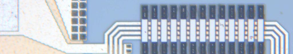
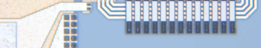
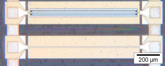
14 Cross-Sectional Image of Inductor in 130 nm 6-level Metal CMOS Process Hard Axis CoZrTa Inductor Metal CoZrTa Magnetic Via Cu (M6) Cu (M5) Cu (M4) Cu (M3) Cu (M2) Cu (M1)
 8 turn (no mag) 4 turn (mag.) 4 turn (no mag) 2 turn (mag.")
 Increase in inductance is small")
15 Spiral Inductors with Single Magnetic Layer Induc ctance (nh) turn (mag.) 8 turn (no mag) 4 turn (mag.) 4 turn (no mag) 2 turn (mag.) 2 turn (no mag) 1 turn (mag.) 1 turn (no mag) Frequency (Hz) Increase in inductance is small (10~30% at up to 9.8 GHz)
16 Spiral Inductors with Two Magnetic Layers Indu uctance (nh) X Frequency (Hz) 8 turn (mag) 8 turn (no mag) 4 turn (solid mag) 4 turn (no mag) 2 turn (solid mag) 2 turn (no mag) 1 turn (solid mag) 1 turn (no mag) Inductance increases by 9


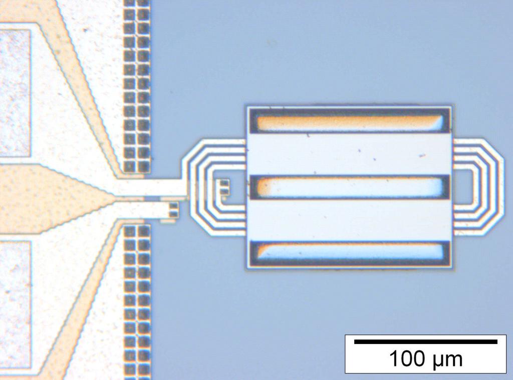
17 Spiral and Stripe Inductors Using 5um thick Copper Hard Easy Structures take advantage of the uniaxial magnetic anisotropy.

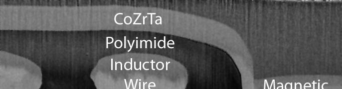
18 Magnetic Via Cross-Sectional Image of Inductor in 90 nm CMOS Process Magnetic Via 90 nm 7-level Metal CMOS Process
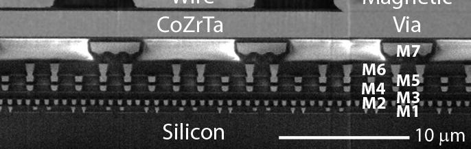
19 Hard Axis Cross-Sectional Image of Inductor
20 Inducta ance (nh) Stripe Inductors With Thick Copper 24X 25X 26X 31X 5 µm mag. 10 µm mag. 20 µm mag. 30 µm mag. 5 µm no mag. 10 µm no mag. 20 µm no mag. 30 µm no mag Frequency (Hz) Inductance increases by up to over 30
 4.0 3.6 3.2 2.8 2.4 2.0 1.6 1.2 0.8 0.4 0.")

21 Magnetic Flux Density At 1GHz Unlaminated Cobalt alloy B-field (T) Laminated Cobalt alloy Skin-depth effect limits penetration of B-field. Larger skin depth results in lower losses.
22 Inductance Modeling of Rectangular Line L µ 0 µ r t m 2 l w l = line length w = line width t m = magnetic film thickness µ r = relative dc permeability 1/L w 1/l L sheet 1/L shunt W tot Eqn. from V. Korenivski and R. B. van Dover, JAP, v. 82 (10), 1997
23 Indu uctance (nh) Magnetic Via Widths 10 µm via 8 µm via 6 µm via 5 µm via 4 µm via thru Frequency (Hz) Inductance increases with via width, but the change becomes diminishingly small.
24 Sheet and Shunt Inductances Sheet inductance (nh/square) um via 8 um via 5 um via 4 um via No mag. alloy Simulated Frequency (Hz) Shunt ind ductance (nh/mm) µm via 8 µm via 5 µm via 4 µm via no mag. alloy Sim. 8 µm via Frequency (Hz) Sheet inductance is independent of the magnetic via width. Shunt inductance increases with increasing via width.
25 Analytical Modeling of Q-Factor Thinner films give higher Q-factors, but lower inductance.
26 Analytical Modeling of Q-Factor Laminations increase the Q-factor.
27 Quality Factor of Inductors With Laminated Magnetic Films 6 4 Q-Factor µm (4 lams) 30 µm (8 lams) 10 µm (4 lams) 10 µm (8 lams) 5 µm (4 lams) 5 µm (8 lams) Frequency (Hz) Peak quality factor is increased, But quality factor at lower frequencies decreased.
28 Summary Magnetic materials Permeability Complex spectra (real and imaginary) Need small coercivity CMOS compatibility (thermal, process compatibility) Inductors Single films increase inductance by 30% up to 9.8 GHz 2 magnetic films increase inductance up to over 30 compared to air-core Over 200 nh inductors possible (1,700 nh/mm 2 ) Sheet inductance vs. shunt inductance Effectiveness of laminated structures Time constants and quality factors Measurements, simulations, and analytical models
29 For More Information IEEE Trans. Magnetics, 45, pp. 4760, Journal of Applied Physics, 103, pp. 07E927, Apr. 1, IEEE Trans. Magnetics, 43, pp. 2615, 2007.
Integrated Inductors with Magnetic Materials for On-Chip Power Conversion
 Integrated Inductors with Magnetic Materials for On-Chip Power Conversion Donald S. Gardner Collaborators: Gerhard Schrom, Fabrice Paillet, Tanay Karnik, Shekhar Borkar Circuits Research Lab & Future Technology
Motivation Different Strategies for Induction integration. Package-Integrated VR with Intel Core 2 Duo Processor. ! Thru-Silicon-Vias (TSV) in future
 in future") Optimization of soft magnetic thin films structures in on-chip inductors for Hao Wu, Donald S. Gardner, and Hongbin Yu Ira A. Fulton Schools of Engineering, Arizona State University, Tempe, AZ8587, United
Optimization of soft magnetic thin films structures in on-chip inductors for Hao Wu, Donald S. Gardner, and Hongbin Yu Ira A. Fulton Schools of Engineering, Arizona State University, Tempe, AZ8587, United
Limitations to Miniaturization of Magnetic Components. Eyal Aklimi, Ph.D. May 2017
 Limitations to Miniaturization of Magnetic Components Eyal Aklimi, Ph.D. May 2017 Outline Background: Why Miniaturize Power Electronics? From Discrete to Integrated Inductors Fabrication Structures Limitations
Microfabrication technologies for highly-laminated thick metallic cores and 3-D integrated windings
 Microfabrication technologies for highly-laminated thick metallic cores and 3-D integrated windings Florian Herrault Georgia Institute of Technology Atlanta, GA florian@gatech.edu http://mems.gatech.edu/msma
Article (peer-reviewed)
") Title Author(s) PCB embedded bondwire inductors with discrete thin film magnetic core for power supply in package Kulkarni, Santosh; Li, Dai; Jordan, Declan; Wang, Ningning; Ó Mathúna, S. Cian Publication
Title Author(s) PCB embedded bondwire inductors with discrete thin film magnetic core for power supply in package Kulkarni, Santosh; Li, Dai; Jordan, Declan; Wang, Ningning; Ó Mathúna, S. Cian Publication
Micro-inductors integrated on silicon for power supply on chip
 Journal of Magnetism and Magnetic Materials 316 (27) e233 e237 www.elsevier.com/locate/jmmm Micro-inductors integrated on silicon for power supply on chip Ningning Wang, Terence O Donnell, Saibal Roy,
INF 5490 RF MEMS. LN12: RF MEMS inductors. Spring 2011, Oddvar Søråsen Department of informatics, UoO
 INF 5490 RF MEMS LN12: RF MEMS inductors Spring 2011, Oddvar Søråsen Department of informatics, UoO 1 Today s lecture What is an inductor? MEMS -implemented inductors Modeling Different types of RF MEMS
Inductors In Silicon Based on SU-8 Enhanced Silicon Molding Technique for Portable Electronics
 Biophotonics & Microsystems Lab Inductors In Silicon Based on SU-8 Enhanced Silicon Molding Technique for Portable Electronics Mingliang Wang 1*, Khai D. T. Ngo 2, Huikai Xie 1 1 BML, University of Florida
Equivalent Circuit Model Overview of Chip Spiral Inductors
 Equivalent Circuit Model Overview of Chip Spiral Inductors The applications of the chip Spiral Inductors have been widely used in telecommunication products as wireless LAN cards, Mobile Phone and so on.
Introduction. Internet of things. Smart New World
 1 Introduction Internet of things Smart New World Source : iamwire IoT has evolved multiple technologies including sensors, embedded systems, communication, real-time analytics or machine learning. For
Integrated on-chip inductors with electroplated magnetic yokes (invited)
") Integrated on-chip inductors with electroplated magnetic yokes (invited) Naigang Wang, Eugene J. O Sullivan, Philipp Herget, Bipin Rajendran, Leslie E. Krupp et al. Citation: J. Appl. Phys. 111, 07E732
Integrated on-chip inductors with electroplated magnetic yokes (invited) Naigang Wang, Eugene J. O Sullivan, Philipp Herget, Bipin Rajendran, Leslie E. Krupp et al. Citation: J. Appl. Phys. 111, 07E732
Radio Frequency Electronics
 Radio Frequency Electronics Preliminaries II Guglielmo Giovanni Maria Marconi Thought off by many people as the inventor of radio Pioneer in long-distance radio communications Shared Nobel Prize in 1909
On-chip Inductors and Transformer
 On-chip Inductors and Transformer Applied Electronics Conference SP1.4 Supply on a Chip - PwrSoC Palm Springs, California 25 Feb 2010 James J. Wang Founder LLC 3131 E. Muirwood Drive Phoenix, Arizona 85048
Chapter 2. Inductor Design for RFIC Applications
 Chapter 2 Inductor Design for RFIC Applications 2.1 Introduction A current carrying conductor generates magnetic field and a changing current generates changing magnetic field. According to Faraday s laws
Integrated On-chip Magnetic-Based Inductors with Externally Applied DC. Magnetic Field for RF and Power Applications.
 Integrated On-chip Magnetic-Based Inductors with Externally Applied DC Magnetic Field for RF and Power Applications by Mahmoud Khdour A Dissertation Presented in Partial Fulfillment of the Requirements
Challenges to Improving the Accuracy of High Frequency (120MHz) Test Systems
 Test Systems") Challenges to Improving the Accuracy of High Frequency (120MHz) Test Systems Applied Power Electronics Conference March 25 th, 2017 Tampa, USA Zoran Pavlovic, Santosh Kulkarni, Satya Kubendran, Cristina
Challenges to Improving the Accuracy of High Frequency (120MHz) Test Systems Applied Power Electronics Conference March 25 th, 2017 Tampa, USA Zoran Pavlovic, Santosh Kulkarni, Satya Kubendran, Cristina
Manufacturing Development of a New Electroplated Magnetic Alloy Enabling Commercialization of PwrSoC Products
 Manufacturing Development of a New Electroplated Magnetic Alloy Enabling Commercialization of PwrSoC Products Trifon Liakopoulos, Amrit Panda, Matt Wilkowski and Ashraf Lotfi PowerSoC 2012 CONTENTS Definitions
Nanomagnetic Structures for Inductive Coupling and Shielding in Wireless Charging Applications
 Nanomagnetic Structures for Inductive Coupling and Shielding in Wireless Charging Applications Dibyajat Mishra, Srikrishna Sitaraman, Saumya Gandhi, Sun Teng, P.M.Raj, Himani Sharma and Rao Tummala T.
OPTIMIZED FRACTAL INDUCTOR FOR RF APPLICATIONS
 OPTIMIZED FRACTAL INDUCTOR FOR RF APPLICATIONS B. V. N. S. M. Nagesh Deevi and N. Bheema Rao 1 Department of Electronics and Communication Engineering, NIT-Warangal, India 2 Department of Electronics and
FABRICATION OF NANO-LAMINATED SOFT MAGNETIC METALLIC ALLOYS THROUGH MULTILAYER ELECTRODEPOSITION: APPLICATION TO HIGH-FREQUENCY
 FABRICATION OF NANO-LAMINATED SOFT MAGNETIC METALLIC ALLOYS THROUGH MULTILAYER ELECTRODEPOSITION: APPLICATION TO HIGH-FREQUENCY AND HIGH-FLUX POWER CONVERSION A Dissertation Presented to The Academic Faculty
Outcomes from this session
 Outcomes from this session At the end of this session you should be able to Understand what is meant by the term losses. Iron Losses There are three types of iron losses Eddy current losses Hysteresis
Iron Powder Cores for High Q Inductors By: Jim Cox - Micrometals, Inc.
 HOME APPLICATION NOTES Iron Powder Cores for High Q Inductors By: Jim Cox - Micrometals, Inc. SUBJECT: A brief overview will be given of the development of carbonyl iron powders. We will show how the magnetic
Microfabricated V-Groove Power Inductors for High-Current Low-Voltage Fast-Transient DC-DC Converters
 Microfabricated V-Groove Power Inductors for High-Current Low-Voltage Fast-Transient DC-DC Converters S. Prabhakaran Yuqin Sun P. Dhagat Weidong Li C. R. Sullivan Found in IEEE Power Electronics Specialists
On-Chip Passive Devices Embedded in Wafer-Level Package
 On-Chip Passive Devices Embedded in Wafer-Level Package Kazuya Masu 1, Kenichi Okada 1, Kazuhisa Itoi 2, Masakazu Sato 2, Takuya Aizawa 2 and Tatsuya Ito 2 On-chip high-q spiral and solenoid inductors
Fabrication and application of a wireless inductance-capacitance coupling microsensor with electroplated high permeability material NiFe
 Journal of Physics: Conference Series Fabrication and application of a wireless inductance-capacitance coupling microsensor with electroplated high permeability material NiFe To cite this article: Y H
Design Strategy of On-Chip Inductors for Highly Integrated RF Systems
 Design Strategy of On-Chip Inductors for Highly Integrated RF Systems C. Patrick Yue T-Span Systems Corporation 44 Encina Drive Palo Alto, CA 94301 (50) 470-51 patrick@tspan.com (Invited Paper) S. Simon
DC-DC Power Conversion with CMOS Integrated Thin-Film Inductors. Noah Sturcken, PhD - Ferric, Inc. CEO
 rric DC-DC Power Conversion with CMOS Integrated Thin-Film Inductors Noah Sturcken, PhD - rric, Inc. CEO FERRIC THE COMPANY Fabless semiconductor technology company, founded in 2011 Located in New York
Achieving High Power Density Designs in DC-DC Converters
 Achieving High Power Density Designs in DC-DC Converters Agenda Marketing / Product Requirement Design Decision Making Translating Requirements to Specifications Passive Losses Active Losses Layout / Thermal
Through-Silicon-Via Inductor: Is it Real or Just A Fantasy?
 Through-Silicon-Via Inductor: Is it Real or Just A Fantasy? Umamaheswara Rao Tida 1 Cheng Zhuo 2 Yiyu Shi 1 1 ECE Department, Missouri University of Science and Technology 2 Intel Research, Hillsboro Outline
S1. Current-induced switching in the magnetic tunnel junction.
 S1. Current-induced switching in the magnetic tunnel junction. Current-induced switching was observed at room temperature at various external fields. The sample is prepared on the same chip as that used
An Automated Design Flow for Synthesis of Optimal Multi-layer Multi-shape PCB Coils for Inductive Sensing Applications
 An Automated Design Flow for Synthesis of Optimal Multi-layer Multi-shape PCB Coils for Inductive Sensing Applications Pradeep Kumar Chawda Texas Instruments Inc., 3833 Kifer Rd, Santa Clara, CA E-mail:
Electromagnetic Interference Shielding Effects in Wireless Power Transfer using Magnetic Resonance Coupling for Board-to-Board Level Interconnection
 Electromagnetic Interference Shielding Effects in Wireless Power Transfer using Magnetic Resonance Coupling for Board-to-Board Level Interconnection Sukjin Kim 1, Hongseok Kim, Jonghoon J. Kim, Bumhee
Magnetic and Electromagnetic Microsystems. 4. Example: magnetic read/write head
 Magnetic and Electromagnetic Microsystems 1. Magnetic Sensors 2. Magnetic Actuators 3. Electromagnetic Sensors 4. Example: magnetic read/write head (C) Andrei Sazonov 2005, 2006 1 Magnetic microsystems
Optimized shield design for reduction of EMF from wireless power transfer systems
 This article has been accepted and published on J-STAGE in advance of copyediting. Content is final as presented. IEICE Electronics Express, Vol.*, No.*, 1 9 Optimized shield design for reduction of EMF
FEM SIMULATION FOR DESIGN AND EVALUATION OF AN EDDY CURRENT MICROSENSOR
 FEM SIMULATION FOR DESIGN AND EVALUATION OF AN EDDY CURRENT MICROSENSOR Heri Iswahjudi and Hans H. Gatzen Institute for Microtechnology Hanover University Callinstrasse 30A, 30167 Hanover Germany E-mail:
High Power Density Power Management IC Module with On-Chip Inductors
 Laboratory for Power Management and Integrated SMPS High Power Density Power Management IC Module with On-Chip Inductors S M Ahsanuzzaman (Ahsan) Aleksandar Prodić David A. Johns Zoran Pavlović Ningning
High Current Inductor Design for MHz Switching
 High Current Inductor Design for MHz Switching M. Duffy *, C. Collins *,F.M.F.Rhen **,P.McCloskey **,S.Roy ** * Power and Energy Research Centre, NUI Galway, Ireland ** Tyndall National Institute, Cork,
3D integrated POL converter
 3D integrated POL converter Presented by: Arthur Ball I- 1 Motivation for this work Today s typical approach for >15A output Point of Load converters: Use PCB material for the entire circuit layout. Need
Inductor Modeling of Integrated Passive Device for RF Applications
 Inductor Modeling of Integrated Passive Device for RF Applications Yuan-Chia Hsu Meng-Lieh Sheu Chip Implementation Center Department of Electrical Engineering 1F, No.1, Prosperity Road I, National Chi
FERRITE CORE INDUCTOR VALUE VARIATION WITH NUMBER OF TURNS AND DIAMETER OF COPPER WIRE,LENGTH AND DIAMETER OF CORE
 FERRITE CORE INDUCTOR VALUE VARIATION WITH NUMBER OF TURNS AND DIAMETER OF COPPER WIRE,LENGTH AND DIAMETER OF CORE PRJ. NO. 073 PRESENTED BY: OMWENGA EDWIN NYAKUNDI F17/8280/2004 SUPERVISOR : MR. OGABA
Impact of Fringing Effects on the Design of DC-DC Converters
 Impact of Fringing Effects on the Design of DC-DC Converters Michael Seeman, Ph.D. Founder / CEO. 2018 APEC PSMA/PELS 2018. Outline Fringe-field loss: What does a power supply designer need to know? Which
1 K Hinds 2012 TRANSFORMERS
 1 K Hinds 2012 TRANSFORMERS A transformer changes electrical energy of a given voltage into electrical energy at a different voltage level. It consists of two coils which are not electrically connected,
Simulation and design of an integrated planar inductor using fabrication technology
 Simulation and design of an integrated planar inductor using fabrication technology SABRIJE OSMANAJ Faculty of Electrical and Computer Engineering, University of Prishtina, Street Sunny Hill, nn, 10000
HOME APPLICATION NOTES
 HOME APPLICATION NOTES INDUCTOR DESIGNS FOR HIGH FREQUENCIES Powdered Iron "Flux Paths" can Eliminate Eddy Current 'Gap Effect' Winding Losses INTRODUCTION by Bruce Carsten for: MICROMETALS, Inc. There
Accurate Models for Spiral Resonators
 MITSUBISHI ELECTRIC RESEARCH LABORATORIES http://www.merl.com Accurate Models for Spiral Resonators Ellstein, D.; Wang, B.; Teo, K.H. TR1-89 October 1 Abstract Analytically-based circuit models for two
Challenges and Trends in Magnetics
 Challenges and Trends in Magnetics Prof. W. G. Hurley Power Electronics Research Centre National University of Ireland, Galway IEEE Distinguished Lecture The University of Hong Kong 27 May 2016 Outline
STUDY AND DESIGN ASPECTS OF INDUCTORS FOR DC-DC CONVERTER
 STUDY AND DESIGN ASPECTS OF INDUCTORS FOR DC-DC CONVERTER 1 Nithya Subramanian, 2 R. Seyezhai 1 UG Student, Department of EEE, SSN College of Engineering, Chennai 2 Associate Professor, Department of EEE,
SUPPLEMENTARY INFORMATION
 Induction of coherent magnetization switching in a few atomic layers of FeCo using voltage pulses Yoichi Shiota 1, Takayuki Nozaki 1, 2,, Frédéric Bonell 1, Shinichi Murakami 1,2, Teruya Shinjo 1, and
FMR and standing spin waves in multifferroics
 FMR and standing spin waves in multifferroics Sławomir Ziętek AGH University of Science and Technology, Department of Electronics, Al. Mickiewicza 3, 3-59 Kraków, Poland Sławomir Ziętek, Nanospin Summarizing
What is an Inductor? Token Electronics Industry Co., Ltd. Version: January 16, Web:
 Version: January 16, 2017 What is an Inductor? Web: www.token.com.tw Email: rfq@token.com.tw Token Electronics Industry Co., Ltd. Taiwan: No.137, Sec. 1, Zhongxing Rd., Wugu District, New Taipei City,
IEEE/CSC & ESAS SUPERCONDUCTIVITY NEWS FORUM
 Kryo 2013 Modern AC Josephson voltage standards at PTB J. Kohlmann, F. Müller, O. Kieler, Th. Scheller, R. Wendisch, B. Egeling, L. Palafox, J. Lee, and R. Behr Physikalisch-Technische Bundesanstalt Φ
Magnetic Spin Devices: 7 Years From Lab To Product. Jim Daughton, NVE Corporation. Symposium X, MRS 2004 Fall Meeting
 Magnetic Spin Devices: 7 Years From Lab To Product Jim Daughton, NVE Corporation Symposium X, MRS 2004 Fall Meeting Boston, MA December 1, 2004 Outline of Presentation Early Discoveries - 1988 to 1995
Shielding Effect of High Frequency Power Transformers for DC/DC Converters used in Solar PV Systems
 Shielding Effect of High Frequency Power Transformers for DC/DC Converters used in Solar PV Systems Author Stegen, Sascha, Lu, Junwei Published 2010 Conference Title Proceedings of IEEE APEMC2010 DOI https://doiorg/101109/apemc20105475521
Ferrochip Design Studio: A New Design Tool for Integrated Magnetics
 Ferrochip Design Studio: A New Design Tool for Integrated Magnetics Ciaran Feeney Ph.D., Ningning Wang Ph.D. Introduction One of the many benefits of integrated magnetics is the ability to optimise the
THE integration and high density trends in electronics have
 5746 IEEE TRANSACTIONS ON POWER ELECTRONICS, VOL. 30, NO. 10, OCTOBER 2015 High Efficiency on Si-Integrated Microtransformers for Isolated Power Conversion Applications Ningning Wang, Member, IEEE, Rais
Non-Ideal Behavior of Components
 Non-Ideal Behavior of Components Todd H. Hubing Dept. of Electrical and Computer Engineering Clemson, University Clemson, SC 29634 USA email: hubing@clemson.edu Telephone: 1-864-656-7219 Circuit Schematics
BGA Solder Balls Formation by Induction Heating
 International Journal of Scientific Research in Knowledge, 2(1), pp. 22-27, 2014 Available online at http://www.ijsrpub.com/ijsrk ISSN: 2322-4541; 2014 IJSRPUB http://dx.doi.org/10.12983/ijsrk-2014-p0022-0027
R. W. Erickson. Department of Electrical, Computer, and Energy Engineering University of Colorado, Boulder
 R. W. Erickson Department of Electrical, Computer, and Energy Engineering University of Colorado, Boulder 13.2.3 Leakage inductances + v 1 (t) i 1 (t) Φ l1 Φ M Φ l2 i 2 (t) + v 2 (t) Φ l1 Φ l2 i 1 (t)
Signal Integrity Design of TSV-Based 3D IC
 Signal Integrity Design of TSV-Based 3D IC October 24, 21 Joungho Kim at KAIST joungho@ee.kaist.ac.kr http://tera.kaist.ac.kr 1 Contents 1) Driving Forces of TSV based 3D IC 2) Signal Integrity Issues
Solving Electromagnetic Interference (EMI) with Ferrites
 with Ferrites") Solving Electromagnetic Interference (EMI) with Ferrites What are ferrites? How do ferrites help Suppress EMI? How to chose proper ferrite and component Material Characteristics Material and Core Selection
Solving Electromagnetic Interference (EMI) with Ferrites What are ferrites? How do ferrites help Suppress EMI? How to chose proper ferrite and component Material Characteristics Material and Core Selection
Fully-Integrated Low Phase Noise Bipolar Differential VCOs at 2.9 and 4.4 GHz
 Fully-Integrated Low Phase Noise Bipolar Differential VCOs at 2.9 and 4.4 GHz Ali M. Niknejad Robert G. Meyer Electronics Research Laboratory University of California at Berkeley Joo Leong Tham 1 Conexant
Optimizing Custom Magnetics for High-Performance Power Supplies
 Optimizing Custom Magnetics for High-Performance Power Supplies Michael Seeman, Ph.D. Founder / CEO. mike@eta1power.com April 2018 PELS Seminar 2018. Outline What is Power Supply Optimization? Performance
Compact Distributed Phase Shifters at X-Band Using BST
 Integrated Ferroelectrics, 56: 1087 1095, 2003 Copyright C Taylor & Francis Inc. ISSN: 1058-4587 print/ 1607-8489 online DOI: 10.1080/10584580390259623 Compact Distributed Phase Shifters at X-Band Using
Modeling and Analysis of Multichip Module Power Supply Planes
 Modeling and Analysis of Multichip Module Power Supply Planes Ken Lee and Alan Barber HPL 94 32 March, 1994 power supply, multi chip module, thin film, thick film, plane, bypass capacitor, switching noise,
TECHNICAL REPORT: CVEL Parasitic Inductance Cancellation for Filtering to Chassis Ground Using Surface Mount Capacitors
 TECHNICAL REPORT: CVEL-14-059 Parasitic Inductance Cancellation for Filtering to Chassis Ground Using Surface Mount Capacitors Andrew J. McDowell and Dr. Todd H. Hubing Clemson University April 30, 2014
Design and Analysis of Novel Compact Inductor Resonator Filter
 Design and Analysis of Novel Compact Inductor Resonator Filter Gye-An Lee 1, Mohamed Megahed 2, and Franco De Flaviis 1. 1 Department of Electrical and Computer Engineering University of California, Irvine
Power SOC Waiting for PSOC. Applications of PSIP/PSOC Products. David I Anderson
 Power SOC 2012 Waiting for PSOC. Applications of PSIP/PSOC Products David I Anderson 1 Overview 1. Introduction 2. Trends and Dislocations 3. Product Trend Setters 4. Inductor Integration Options 5. Why
ETI , Good luck! Written Exam Integrated Radio Electronics. Lund University Dept. of Electroscience
 und University Dept. of Electroscience EI170 Written Exam Integrated adio Electronics 2010-03-10, 08.00-13.00 he exam consists of 5 problems which can give a maximum of 6 points each. he total maximum
Permeability Measurements of Very Thin Magnetic Film Using a Flexible Microstrip-Line-Type Probe
 J. Magn. Soc. Jpn., 39, -5 (25) Permeability Measurements of Very Thin Magnetic Film Using a Flexible Microstrip-Line-Type Probe K. Kusunoki, S. Yabukami*, T. Ozawa*, H. Uetake*, H. Yamada, Y.
West Coast Magnetics. Advancing Power Electronics FOIL WINDINGS FOR SMPS INDUCTORS AND TRANSFORMERS. Weyman Lundquist, CEO and Engineering Manager
 1 West Coast Magnetics Advancing Power Electronics FOIL WINDINGS FOR SMPS INDUCTORS AND TRANSFORMERS Weyman Lundquist, CEO and Engineering Manager TYPES OF WINDINGS 2 Solid wire Lowest cost Low DC resistance
Package and Integration Technology in Point-of-load Converters. Laili Wang Xi an Jiaotong University Sumida Technology
 Package and Integration Technology in Point-of-load Converters Laili Wang Xi an Jiaotong University Sumida Technology Content Introduction Multi-permeability distributed air-gap inductor Multi-permeability
University oftokyo. LSI esign & ducation enter
 Analysis on An Interconnections in V Hi-Frequency Mido and Kunihiro Asada Tetsuhisa Electronic Engineering Dept. Considering Inductive Eects (V Design and E C (VDEC)), Mar. 9th, 999 Dept. E.E., Univ..
Broadband analog phase shifter based on multi-stage all-pass networks
 This article has been accepted and published on J-STAGE in advance of copyediting. Content is final as presented. IEICE Electronics Express, Vol.* No.*,*-* Broadband analog phase shifter based on multi-stage
Integrated Electroplated Micromachined Magnetic Devices Using Low Temperature Fabrication Processes
 48 IEEE TRANSACTIONS ON ELECTRONICS PACKAGING MANUFACTURING, VOL. 23, NO. 1, JANUARY 2000 Integrated Electroplated Micromachined Magnetic Devices Using Low Temperature Fabrication Processes Jae Yeong Park,
Analysis of High Efficiency Multistage Matching Networks with Volume Constraint
 Analysis of High Efficiency Multistage Matching Networks with Volume Constraint Phyo Aung Kyaw, Aaron.F. Stein, Charles R. Sullivan Thayer School of Engineering at Dartmouth Hanover, NH 03755, USA {phyo.a.kyaw.th,
Efficient Electromagnetic Analysis of Spiral Inductor Patterned Ground Shields
 Efficient Electromagnetic Analysis of Spiral Inductor Patterned Ground Shields James C. Rautio, James D. Merrill, and Michael J. Kobasa Sonnet Software, North Syracuse, NY, 13212, USA Abstract Patterned
A Small Area 5GHz LC VCO with an On-Chip Solenoid Inductor using a 0.13μm Digital CMOS Technology
 A Small Area 5GHz LC VCO with an On-Chip Solenoid Inductor using a 0.3μm Digital CMOS Technology Chul Nam, Byeungleul Lee 2, Tae-Young Byun 3, Yongjun Jon 4, and Bonghwan Kim 5,* R&D Center/Siliconharmony,
Trough-silicon-via inductor: Is it real or just a fantasy?
 Scholars' Mine Masters Theses Student Research & Creative Works Fall 2013 Trough-silicon-via inductor: Is it real or just a fantasy? Rongbo Yang Follow this and additional works at: http://scholarsmine.mst.edu/masters_theses
EE2022 Electrical Energy Systems
 EE0 Electrical Energy Systems Lecture : Transformer and Per Unit Analysis 7-0-0 Panida Jirutitijaroen Department of Electrical and Computer Engineering /9/0 EE0: Transformer and Per Unit Analysis by P.
Chapter 2-1 Transformers
 Principles of Electric Machines and Power Electronics Chapter 2-1 Transformers Third Edition P. C. Sen Transformer application 1: power transmission Ideal Transformer Assumptions: 1. Negligible winding
Physical Modeling of Spiral Inductors on Silicon
 560 IEEE TRANSACTIONS ON ELECTRON DEVICES, VOL. 47, NO. 3, MARCH 2000 Physical Modeling of Spiral Inductors on Silicon C. Patrick Yue, Member, IEEE, and S. Simon Wong, Fellow, IEEE Abstract This paper
ISSCC 2006 / SESSION 11 / RF BUILDING BLOCKS AND PLLS / 11.9
 ISSCC 2006 / SESSION 11 / RF BUILDING BLOCKS AND PLLS / 11.9 11.9 A Single-Chip Linear CMOS Power Amplifier for 2.4 GHz WLAN Jongchan Kang 1, Ali Hajimiri 2, Bumman Kim 1 1 Pohang University of Science
AN ABSTRACT OF THE THESIS OF
 AN ABSTRACT OF THE THESIS OF Arien Sligar for the degree of Master of Science in Electrical and Computer Engineering presented on August 18, 2006. Title: On-Chip Crosstalk Suppression Schemes using Magnetic
Optical Bus for Intra and Inter-chip Optical Interconnects
 Optical Bus for Intra and Inter-chip Optical Interconnects Xiaolong Wang Omega Optics Inc., Austin, TX Ray T. Chen University of Texas at Austin, Austin, TX Outline Perspective of Optical Backplane Bus
Introduction to Microeletromechanical Systems (MEMS) Lecture 12 Topics. MEMS Overview
 Lecture 12 Topics. MEMS Overview") Introduction to Microeletromechanical Systems (MEMS) Lecture 2 Topics MEMS for Wireless Communication Components for Wireless Communication Mechanical/Electrical Systems Mechanical Resonators o Quality
Introduction to Microeletromechanical Systems (MEMS) Lecture 2 Topics MEMS for Wireless Communication Components for Wireless Communication Mechanical/Electrical Systems Mechanical Resonators o Quality
Design of MEMS Tunable Inductor Implemented on SOI and Glass wafers Using Bonding Technology
 Design of MEMS Tunable Inductor Implemented on SOI and Glass wafers Using Bonding Technology USAMA ZAGHLOUL* AMAL ZAKI* HAMED ELSIMARY* HANI GHALI** and HANI FIKRI** * Electronics Research Institute, **
Topic 4 Practical Magnetic Design: Inductors and Coupled Inductors
 Topic 4 Practical Magnetic Design: Inductors and Coupled Inductors Louis Diana Agenda Theory of operation and design equations Design flow diagram discussion Inductance calculations Ampere s law for magnetizing
Optimization of Symmetric Spiral Inductors On Silicon Substrate
 Optimization of Symmetric Spiral Inductors On Silicon Substrate Hyunjin Lee, Joonho Gil, and Hyungcheol Shin Department of Electrical Engineering and Computer Science, KAIST -1, Guseong-dong, Yuseong-gu,
TRAFTOR WINDINGS CHANGING THE RULES TOROIDAL INDUCTORS & TRANSFORMERS SOLUTIONS PROVIDER AND MANUFACTURER
 TRAFTOR WINDINGS CHANGING THE RULES TOROIDAL INDUCTORS & TRANSFORMERS SOLUTIONS PROVIDER AND MANUFACTURER PRODUCT RANGE POWER INDUCTORS Toroidal technology, driven by 20 years of R&D. POWER TRANSFORMERS
Enabling Resonant Clock Distribution with Scaled On-Chip Magnetic Inductors
 Enabling Resonant Clock Distribution with Scaled On-Chip Magnetic Inductors Saurabh Sinha, Wei Xu, Jyothi B. Velamala, Tawab Dastagir, Bertan Bakkaloglu, Hongbin Yu and Yu Cao Department of Electrical
In-circuit Measurements of Inductors and Transformers in Switch Mode Power Supplies APPLICATION NOTE
 In-circuit Measurements of Inductors and Transformers in Switch Mode Power Supplies FIGURE 1. Inductors and transformers serve key roles in switch mode power supplies, including filters, step-up/step-down,
An Equivalent Circuit Model for On-chip Inductors with Gradual Changed Structure
 An Equivalent Circuit Model for On-chip Inductors with Gradual Changed Structure Xi Li 1, Zheng Ren 2, Yanling Shi 1 1 East China Normal University Shanghai 200241 People s Republic of China 2 Shanghai
Synthesis of Optimal On-Chip Baluns
 Synthesis of Optimal On-Chip Baluns Sharad Kapur, David E. Long and Robert C. Frye Integrand Software, Inc. Berkeley Heights, New Jersey Yu-Chia Chen, Ming-Hsiang Cho, Huai-Wen Chang, Jun-Hong Ou and Bigchoug
PRINTED CIRCUIT BOARD WINDINGS-BASED ULTRA LOW-PROFILE POWER CONDITIONING CIRCUITS FOR SDR APPLICATION SYSTEMS
 PRINTED CIRCUIT BOARD WINDINGS-BASED ULTRA LOW-PROFILE POWER CONDITIONING CIRCUITS FOR SDR APPLICATION SYSTEMS Wonseok Lim ( Kyungpook National University, Taegu, Korea; iws95@ee.knu.ac.kr); Dongsoo Kim
ABabcdfghiejklStanford University
 Design Methodology or Power-Constrained Low Noise RF Circuits Jung-Suk Goo, Hee-Tae Ahn, Donald J Ladwig, Zhiping Yu, Thomas H Lee, and Robert W Dutton, Stanord University, Stanord CA National Semiconductor,
A Planar Fractal Micro-Transformer with Air Core and Hilbert Curve
 A Planar Fractal Micro-Transformer with Air Core and Hilbert Curve Yong Zhu Fahimullah Khan Junwei Lu Dzung Viet Dao Abstract: In this paper, a novel MEMS-based planar fractal transformer is presented.
Trends and Challenges in VLSI Technology Scaling Towards 100nm
 Trends and Challenges in VLSI Technology Scaling Towards 100nm Stefan Rusu Intel Corporation stefan.rusu@intel.com September 2001 Stefan Rusu 9/2001 2001 Intel Corp. Page 1 Agenda VLSI Technology Trends
Microfabricated Coupled-Inductors for DC-DC Converters for Microprocessor Power Delivery
 Microfabricated Coupled-Inductors for DC-DC Converters for Microprocessor Power Delivery S. Prabhakaran T. O Donnell C. O Mathuna C. R. Sullivan Found in IEEE Power Electronics Specialists Conference,
A GSM Band Low-Power LNA 1. LNA Schematic
 A GSM Band Low-Power LNA 1. LNA Schematic Fig1.1 Schematic of the Designed LNA 2. Design Summary Specification Required Simulation Results Peak S21 (Gain) > 10dB >11 db 3dB Bandwidth > 200MHz (
Ultra Low Inductance Package for SiC & GaN
 Ultra Low Inductance Package for SiC & GaN Dr.-Ing. Eckart Hoene Powered by Overview The Motivation The Modules The Semiconductors The Measurement Equipment The Simulation The Results The Conclusion Motivation