Ultra Low Inductance Package for SiC & GaN
|
|
|
- Hugh Atkinson
- 5 years ago
- Views:
Transcription

1 Ultra Low Inductance Package for SiC & GaN Dr.-Ing. Eckart Hoene Powered by
2 Overview The Motivation The Modules The Semiconductors The Measurement Equipment The Simulation The Results The Conclusion
3 Motivation Semiconductors made of high band gap material are a step further towards to ideal switch The switching behavior of an ideal switch is dominated by the electromagnetic properties of its package How can we adapt the semiconductor packaging technologies and the design concept to the upcomming needs?
4 Motivation Design goals are e.g. low DC-link inductance values or reduced electromagnetic interference spreading out from the switch In power electronics well known strategy to reduce inductance is the bus bar design: i fwd i back Two flat conductors with 0.5mm distance, 30mm width and 10cm length show a return inductance of 2.1nH d L * l * * in µh B l : length of the conductors in cm d B : distance : width of of the conductors conductors
5 The more conventional style module Idea: using wire bonds for semiconductor interconnection and bus bars for DC link Low inductance interconnect between module and PCB with DC capacitors


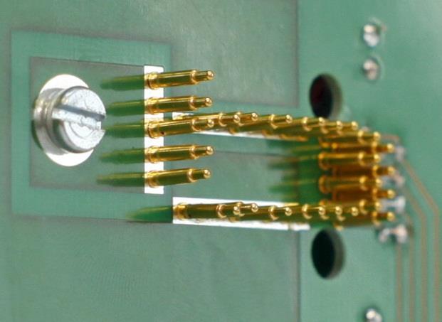
6 The more conventional style module Internal module Busbars Screw PCB Path of the DC link current DBC Semiconductors Cross section through the module including PCB and pressed interconnection


7 The more conventional style module System setup Driver board DC link

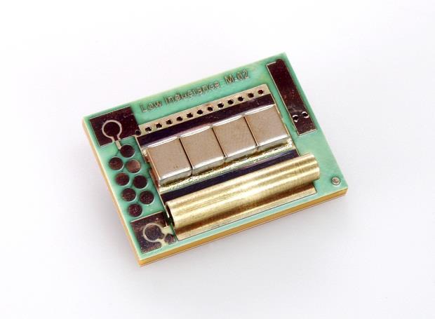
8 The embedded module Current measurement DC link capacitors Full bus bar structure using PCB Process on a DBC DCB DC- JFET Gates Out DC+ DC capacitors on the module DC link current measurement included Diode Abb. 1: Explosionsansicht des Modulaufbaus


9 The embedded module 3 active layers (DBC, Interlayer 60µm, Toplayer 100µm) Semiconductors sintered on bottom and stud bumps on top to be compatible with galvanisation 1.8µF on module 100 µm Toplayer 100 µm Prepreg 60 µm Interlayer 100 µm Preprag + Stud Bumps 300 µm Chip 100 µm Solder 300 µm Copper 380 µm Al 2 O µm Copper


10 Low Induction - Process Flow Step 1 Assembly the J-Fets on the DCB by sintering Step 2 Bonding gold-stud-bumbs on the aluminium pads To handle single DCB-ceramics with 2cm x 3cm outline in a production line it is needed a transport substrate Step 3 production of a transport substrate and mounting the DCBs on it Step 4 Lamination of prepregs and Cu-foil for the middle layer The best possible method to contact the Au-stud-bumps is by mechanical milling Step 5 Depth controlled milling through the epoxy exactly into the bumps and drilling of the first blind vias


11 Low Induction - Process Flow Step 6 Galvanic deposition of a copper layer with a thickness of 60µm in preparation to lamination of the photo resist it is required a Step 7 Printing of a paste in the cavities to equalize the surface Step 8 Structuring the copper middle layer over the J-Fets by exposure and chemical etching Step 9 Second lamination of prepreg and Cu-foil for the top layer Step 10 Drilling of blind vias to the ground and the middle layer


12 Low Induction - Process Flow Step 11 Galvanic deposition of a copper layer with a thickness of 100µm Step 12 Structuring the top layer by etching Step 13 Singularize the modules by milling

13 The embedded module DC- Driver Output DC+ Mounts for Voltage Probes

14 The embedded module
15 The Semiconductors First selection: Semisouth normally off (47mΩ/1200V) with a schottky free wheeling diode and a Semisouth driver. This configuration could not be brought to work within the restricted number of modules produced Second selection: Infineon 100mΩ/1200V with included parasitic freewheeling diode. All shown measurements were carried out with this semiconductors


16 The Measurement Equipment Current path Requirements: high bandwidth, low influence on setup, high noise immunity Solution for current sensor: A Rogowski coil placed in an Ω-shaped brass tube, the voltage across the coil measured with a 1GHz low capacitance probe and an oscilloscope Achieved bandwidth: 500MHz Shielded construction 300pH added inductance

17 The Simulation DC link inductance of the conventional module
 comm L 1.")
18 The Simulation Embedded module L 0.67 nh ( without _ primary _ coil) comm L 1.1 nh ( with _ primary _ coil) L comm coil, prim. 0.43nH

19 The Results Embedded module V_DS I_Coil V_Shunt

20 The Results Embedded module Switch on at 0A: Voltage slope 10V/ns Current peak due to internal capacitance I D (1Vs = 1A)
21 The Results Embedded module Switch off at 20A: Voltage slope 22V/ns Current slope max. 4A/ns (50% to 90%) Low overshot (approx. 10V) very little ringing (frequency 240 MHz) I D (1Vs = 1A)


22 The Results Embedded module Switch on at 20A: Voltage slope 10V/ns Current slope 3.13A/ns I D (1Vs = 1A)

23 The Results Damped oscillation after turn-off Turn-off 40V f C res oss MHz 522 pf 1 f res Lcomm 0.866nH 2 C L oss comm Determining of the commutation inductance
24 The Results Observation: Parasitic switch on - intrinsic parasitic capacitances of JFET: Cgd, Cgs, Cds - parasitic influence of wire: Lg_par, Ls_par, Rs_par Cgd-measurement => simulation

25 The Results E1 /V V GS /V time/s assumption: Cds 3xCgd t rise = 25 ns V ds = 600 V V gs = V Cgd =f(uds) look-up table without L s_par with L s_par time/s
26 Outlook The developed package is to good for the switch, even significantly faster switches could be packaged this way The proposed packaging technology leads the way to a package for the ideal switch. Ideal switches will have to be packaged including the commutation cell, in order to make it possible to handle for the average user
Ultra-Low-Inductance Power Module for Fast Switching Seminconductors
 2013 Mesago PCIM GmbH Proceedings of the PCIM Europe Conference for Power Electronics, Intelligent Motion, Renewable Energy and Energy Management, Nuremberg, Germany, 14-16 May 2013 Ultra-Low-Inductance
Current sensor by IZM
 Current sensor by IZM TYPICAL APPLICATIONS Current measurement in commutation cell Monitoring of switching behavior of Si, SiC, GaN, or similar semiconductors Measuring of current pulses Analysis of power
Current sensor demonstrator by IZM
 Current sensor demonstrator by IZM TYPICAL APPLICATIONS Current measurement in commutation cell Monitoring of switching behavior of Si, SiC, GaN, or similar semiconductor devices Measuring of current pulses
Double Pulse Test Board
 Double Pulse Test Board Features 1200 V, 100 A Testing Low Series Inductance Design Wide, 6 oz. Copper Current Traces Multiple DUT and FWD Connections for Long Life Compatible with GeneSiC Gate Drive Mounting
Memo. 1 Summary. 1.1 Introduction. 1.2 Experiments. 1.3 Conclusion
 Topic: Tested: Date: Author: High frequency oscillations measured with high bandwidth current sensors at low current Pearson 2878 and SDN-414 shunts with different resistance values 2014 April 11 th Martin
Medium-Voltage SiC Power MOSFET Packaging: An International Collaboration
 Centre for Power Electronics Annual Conference Loughborough, UK Medium-Voltage SiC Power MOSFET Packaging: An International Collaboration Christina DiMarino, Bassem Mouawad, Mark Johnson, Dushan Boroyevich,
Low-inductive inverter concept by 200 A / 1200 V half bridge in an EasyPACK 2B following strip-line design
 Low-inductive inverter concept by 200 A / 1200 V half bridge in an EasyPACK 2B following strip-line design Dr. Christian R. Müller and Dr. Reinhold Bayerer, Infineon Technologies AG, Max-Planck- Straße
Fast switching and its challenges on Power Module Packaging and System Design
 Fast switching and its challenges on Power Module Packaging and System Design Power Electronic Conference Munich 05/12/2017 Stefan Häuser Product Marketing International stefan.haeuser@semikron.com Johannes
Symbol Parameter Typical
 PRODUCT SUMMARY (TYPICAL) V DS (V) 600 R DS(on) ( ) 0.29 Q rr (nc) 29 Features Low Q rr Free-wheeling diode not required Low-side Quiet Tab for reduced EMI RoHS compliant High frequency operation Applications
Driving IGBTs with unipolar gate voltage
 Page 1 Driving IGBTs with unipolar gate voltage Introduction Infineon recommends the use of negative gate voltage to safely turn-off and block IGBT modules. In areas with nominal currents less than 100tA
Understanding and Optimizing Electromagnetic Compatibility in Switchmode Power Supplies
 Understanding and Optimizing Electromagnetic Compatibility in Switchmode Power Supplies 1 Definitions EMI = Electro Magnetic Interference EMC = Electro Magnetic Compatibility (No EMI) Three Components
SiC-JFET in half-bridge configuration parasitic turn-on at
 SiC-JFET in half-bridge configuration parasitic turn-on at current commutation Daniel Heer, Infineon Technologies AG, Germany, Daniel.Heer@Infineon.com Dr. Reinhold Bayerer, Infineon Technologies AG, Germany,
3D integrated POL converter
 3D integrated POL converter Presented by: Arthur Ball I- 1 Motivation for this work Today s typical approach for >15A output Point of Load converters: Use PCB material for the entire circuit layout. Need
PC Krause and Associates, Inc.
 Common-mode challenges in high-frequency switching converters 14 NOV 2016 Nicholas Benavides, Ph.D. (Sr. Lead Engineer) 3000 Kent Ave., Suite C1-100 West Lafayette, IN 47906 (765) 464-8997 (Office) (765)
Practical Measurements considerations for GaN and SiC technologies ANDREA VINCI EMEA MARKET DEVELOPMENT MANAGER POWER ELECTRONICS
 Practical Measurements considerations for GaN and SiC technologies ANDREA VINCI EMEA MARKET DEVELOPMENT MANAGER POWER ELECTRONICS PLEASED TO MEET YOU 2 Evolving Test Solutions with Semiconductors WAFER
GS61008P Bottom-side cooled 100 V E-mode GaN transistor Preliminary Datasheet
 Features 100 V enhancement mode power switch Bottom-side cooled configuration R DS(on) = 7 mω I DS(max) = 90 A Ultra-low FOM Island Technology die Low inductance GaNPX package Easy gate drive requirements
77 GHz VCO for Car Radar Systems T625_VCO2_W Preliminary Data Sheet
 77 GHz VCO for Car Radar Systems Preliminary Data Sheet Operating Frequency: 76-77 GHz Tuning Range > 1 GHz Output matched to 50 Ω Application in Car Radar Systems ESD: Electrostatic discharge sensitive
GaN is Crushing Silicon. EPC - The Leader in GaN Technology IEEE PELS
 GaN is Crushing Silicon EPC - The Leader in GaN Technology IEEE PELS 2014 www.epc-co.com 1 Agenda How egan FETs work Hard Switched DC-DC converters High Efficiency point-of-load converter Envelope Tracking
Double Pulse Switching Board
 Double Pulse Switching Board Features 1200 V, 100 A Testing Low Series Inductance Design Wide, 6 oz. Copper Current Traces Multiple DUT and FWD Connections for Durability Low Resistance and Inductance
GS61008T Top-side cooled 100 V E-mode GaN transistor Preliminary Datasheet
 Features 100 V enhancement mode power switch Top-side cooled configuration R DS(on) = 7 mω I DS(max) = 90 A Ultra-low FOM Island Technology die Low inductance GaNPX package Easy gate drive requirements
Application Note 0009
 Recommended External Circuitry for Transphorm GaN FETs Application Note 9 Table of Contents Part I: Introduction... 2 Part II: Solutions to Suppress Oscillation... 2 Part III: The di/dt Limits of GaN Switching
SiC MOSFETs Based Split Output Half Bridge Inverter: Current Commutation Mechanism and Efficiency Analysis
 SiC MOSFETs Based Split Output Half Bridge Inverter: Current Commutation Mechanism and Efficiency Analysis Helong Li, Stig Munk-Nielsen, Szymon Bęczkowski, Xiongfei Wang Department of Energy Technology
NPA105-D. Preliminary GHz GaN 40W Power Amplifier. Product Description: Key Features:
 Product Description: The Nxbeam is a Ku-band high power GaN MMIC fabricated in 0.2um GaN HEMT on SiC. This part is ideally suited for satellite communications, point-to-point radios, and radar applications.
GS66516T Top-side cooled 650 V E-mode GaN transistor Preliminary Datasheet
 Features 650 V enhancement mode power switch Top-side cooled configuration R DS(on) = 25 mω I DS(max) = 60 A Ultra-low FOM Island Technology die Low inductance GaNPX package Easy gate drive requirements
AN-5077 Design Considerations for High Power Module (HPM)
") www.fairchildsemi.com AN-5077 Design Considerations for High Power Module (HPM) Abstract Fairchild s High Power Module (HPM) solution offers higher reliability, efficiency, and power density to improve
www.fairchildsemi.com AN-5077 Design Considerations for High Power Module (HPM) Abstract Fairchild s High Power Module (HPM) solution offers higher reliability, efficiency, and power density to improve
A large-area wireless power transmission sheet using printed organic. transistors and plastic MEMS switches
 Supplementary Information A large-area wireless power transmission sheet using printed organic transistors and plastic MEMS switches Tsuyoshi Sekitani 1, Makoto Takamiya 2, Yoshiaki Noguchi 1, Shintaro
Taking advantage of SiC s high switching speeds with optimizations in measurement, layout, and design
 Taking advantage of SiC s high switching speeds with optimizations in measurement, layout, and design Dr. Kevin M. Speer Global Manager of Technology Strategy Power Semiconductors Power Electronics Conference
Symbol Parameter Typical
 PRODUCT SUMMARY (TYPICAL) V DS (V) 650 R DS(on) (m ) 110 Q rr (nc) 54 Features Low Q rr Free-wheeling diode not required Low-side Quiet Tab for reduced EMI RoHS compliant High frequency operation Applications
GS66508T Top-side cooled 650 V E-mode GaN transistor Preliminary Datasheet
 Features 650 V enhancement mode power switch Top-side cooled configuration R DS(on) = 50 mω I DS(max) = 30 A Ultra-low FOM Island Technology die Low inductance GaNPX package Easy gate drive requirements
Limiter Diodes Features Description Chip Dimensions Model DOT Diameter (Typ.) Chip Number St l Style Inches 4 11
 Chip Number St l Style Inches 4 11") Features Low Loss kw Coarse Limiters 200 Watt Midrange Limiters 10 mw Clean Up Limiters 210 20 Description Alpha has pioneered the microwave limiter diode. Because all phases of manufacturing, from design
Features Low Loss kw Coarse Limiters 200 Watt Midrange Limiters 10 mw Clean Up Limiters 210 20 Description Alpha has pioneered the microwave limiter diode. Because all phases of manufacturing, from design
Physical RF Circuit Techniques and Their Implications on Future Power Module and Power Electronic Design
 Physical RF Circuit Techniques and Their Implications on Future Power Module and Power Electronic Design Adam Morgan 5-5-2015 NE IMAPS Symposium 2015 Overall Motivation Wide Bandgap (WBG) semiconductor
The practicalities of measuring fast switching currents in power electronics using Rogowski probes
 The practicalities of measuring fast switching currents in power electronics using Rogowski probes Dr Chris Hewson Director, PEM Ltd Booth No. 418 About PEM Ltd Power Electronic Measurements Ltd (PEM)
Design and Characterization of a Three-Phase Multichip SiC JFET Module
 Design and Characterization of a Three-Phase Multichip SiC JFET Module Fan Xu* fxu6@utk.edu Jing Wang* jwang50@utk.edu Dong Jiang* djiang4@utk.edu Fred Wang* fred.wang@utk.edu Leon Tolbert* tolbert@utk.edu
Raffael Schnell, Product Manager, ABB Switzerland Ltd, Semiconductors LinPak a new low inductive phase-leg IGBT module ABB
 Raffael Schnell, Product Manager, ABB Switzerland Ltd, Semiconductors LinPak a new low inductive phase-leg IGBT module Slide 1 The LinPak Main features Low inductive target inductance 1 nh, ready for fast
All-SiC Modules Equipped with SiC Trench Gate MOSFETs
 All-SiC Modules Equipped with SiC Trench Gate MOSFETs NAKAZAWA, Masayoshi * DAICHO, Norihiro * TSUJI, Takashi * A B S T R A C T There are increasing expectations placed on products that utilize SiC modules
NPA110-D. Preliminary GHz GaN 38W Power Amplifier. Product Description: Key Features:
 NPA1-D Product Description: The Nxbeam NPA1-D is a Ka-band high power GaN MMIC fabricated in.2um GaN HEMT on SiC. This part is ideally suited for satellite communications, point-to-point radios, and radar
New fabrication and packaging technologies for CMOS pixel sensors: closing gap between hybrid and monolithic
 New fabrication and packaging technologies for CMOS pixel sensors: closing gap between hybrid and monolithic Outline Short history of MAPS development at IPHC Results from TowerJazz CIS test sensor Ultra-thin
GS61004B 100V enhancement mode GaN transistor Preliminary Datasheet
 Features 100V enhancement mode power switch Bottom-side cooled configuration R DS(on) = 15 mω I DS(max) = 45 A Ultra-low FOM Island Technology die Low inductance GaNPX package Easy gate drive requirements
Flip-Chip for MM-Wave and Broadband Packaging
 1 Flip-Chip for MM-Wave and Broadband Packaging Wolfgang Heinrich Ferdinand-Braun-Institut für Höchstfrequenztechnik (FBH) Berlin / Germany with contributions by F. J. Schmückle Motivation Growing markets
Digital Integrated Circuits Lecture 20: Package, Power, Clock, and I/O
 Digital Integrated Circuits Lecture 20: Package, Power, Clock, and I/O Chih-Wei Liu VLSI Signal Processing LAB National Chiao Tung University cwliu@twins.ee.nctu.edu.tw DIC-Lec20 cwliu@twins.ee.nctu.edu.tw
ELEC-E8421 Components of Power Electronics
 ELEC-E8421 Components of Power Electronics MOSFET 2015-10-04 Metal-Oxide-Semiconductor Field-Effect-Transistor (MOSFET) Vertical structure makes paralleling of many small MOSFETs on the chip easy. Very
GS66502B Bottom-side cooled 650 V E-mode GaN transistor Preliminary Datasheet
 GS66502B Features 650 V enhancement mode power switch Bottom-side cooled configuration R DS(on) = 200 mω I DS(max) = 7.5 A Ultra-low FOM Island Technology die Low inductance GaNPX package Easy gate drive
Digital Systems Power, Speed and Packages II CMPE 650
 Speed VLSI focuses on propagation delay, in contrast to digital systems design which focuses on switching time: A B A B rise time propagation delay Faster switching times introduce problems independent
IRHNA57264SE JANSR2N7474U2 R 5 250V, N-CHANNEL REF: MIL-PRF-19500/684 RADIATION HARDENED POWER MOSFET SURFACE MOUNT (SMD-2) PD-93816G TECHNOLOGY
 PD-93816G TECHNOLOGY") PD-9386G IRHNA57264SE RADIATION HARDENED POWER MOSFET SURFACE MOUNT (SMD-2) 25V, N-CHANNEL REF: MIL-PRF-95/684 R 5 TECHNOLOGY Product Summary Part Number Radiation Level RDS(on) I D QPL Part Number IRHNA57264SE
PD-9386G IRHNA57264SE RADIATION HARDENED POWER MOSFET SURFACE MOUNT (SMD-2) 25V, N-CHANNEL REF: MIL-PRF-95/684 R 5 TECHNOLOGY Product Summary Part Number Radiation Level RDS(on) I D QPL Part Number IRHNA57264SE
IRHNJ57230SE JANSR2N7486U3 R 5 200V, N-CHANNEL REF: MIL-PRF-19500/704 RADIATION HARDENED POWER MOSFET SURFACE MOUNT (SMD-0.5) PD-93836C TECHNOLOGY
 PD-93836C TECHNOLOGY") PD-93836C IRHNJ5723SE RADIATION HARDENED POWER MOSFET SURFACE MOUNT (SMD-.5) 2V, N-CHANNEL REF: MIL-PRF-95/74 R 5 TECHNOLOGY Product Summary Part Number Radiation Level RDS(on) I D QPL Part Number IRHNJ5723SE
PD-93836C IRHNJ5723SE RADIATION HARDENED POWER MOSFET SURFACE MOUNT (SMD-.5) 2V, N-CHANNEL REF: MIL-PRF-95/74 R 5 TECHNOLOGY Product Summary Part Number Radiation Level RDS(on) I D QPL Part Number IRHNJ5723SE
GS66516B Bottom-side cooled 650 V E-mode GaN transistor Preliminary Datasheet
 Features 650 V enhancement mode power switch Bottom-side cooled configuration R DS(on) = 25 mω I DS(max) = 60 A Ultra-low FOM Island Technology die Low inductance GaNPX package Easy gate drive requirements
Customized probe card for on-wafer testing of AlGaN/GaN power transistors
 Customized probe card for on-wafer testing of AlGaN/GaN power transistors R. Venegas 1, K. Armendariz 2, N. Ronchi 1 1 imec, 2 Celadon Systems Inc. Outline Introduction GaN for power switching applications
GS66508P Bottom-side cooled 650 V E-mode GaN transistor Preliminary Datasheet
 Features 650 V enhancement mode power switch Bottom-side cooled configuration R DS(on) = 50 mω I DS(max) = 30 A Ultra-low FOM Island Technology die Low inductance GaNPX package Easy gate drive requirements
GS66516B Bottom-side cooled 650 V E-mode GaN transistor Preliminary Datasheet
 Features 650 V enhancement mode power switch Bottom-side cooled configuration R DS(on) = 25 mω I DS(max) = 60 A Ultra-low FOM Island Technology die Low inductance GaNPX package Easy gate drive requirements
A GSM Band Low-Power LNA 1. LNA Schematic
 A GSM Band Low-Power LNA 1. LNA Schematic Fig1.1 Schematic of the Designed LNA 2. Design Summary Specification Required Simulation Results Peak S21 (Gain) > 10dB >11 db 3dB Bandwidth > 200MHz (
Signal Integrity Design of TSV-Based 3D IC
 Signal Integrity Design of TSV-Based 3D IC October 24, 21 Joungho Kim at KAIST joungho@ee.kaist.ac.kr http://tera.kaist.ac.kr 1 Contents 1) Driving Forces of TSV based 3D IC 2) Signal Integrity Issues
GS61004B 100V enhancement mode GaN transistor Preliminary Datasheet
 Features 100V enhancement mode power switch Bottom-side cooled configuration R DS(on) = 15 mω I DS(max) = 45 A Ultra-low FOM Island Technology die Low inductance GaNPX package Easy gate drive requirements
NPA100-D GHz GaN 20W Power Amplifier. Product Description: Key Features:
 Product Description: The Nxbeam is a Ku-band high power GaN MMIC fabricated in 0.2um GaN HEMT on SiC. This part is ideally suited for satellite communications, point-to-point radios, and radar applications.
POWER MOSFET SURFACE MOUNT (SMD-1) 200V, N-CHANNEL. Absolute Maximum Ratings PD-94236C
 200V, N-CHANNEL. Absolute Maximum Ratings PD-94236C") PD-94236C RADIATION HARDENED POWER MOSFET SURFACE MOUNT (SMD-) IRHN5725SE 2V, N-CHANNEL 5 TECHNOLOGY Product Summary Part Number Radiation Level RDS(on) ID IRHN5725SE K Rads (Si).6Ω 3A SMD- International
PD-94236C RADIATION HARDENED POWER MOSFET SURFACE MOUNT (SMD-) IRHN5725SE 2V, N-CHANNEL 5 TECHNOLOGY Product Summary Part Number Radiation Level RDS(on) ID IRHN5725SE K Rads (Si).6Ω 3A SMD- International
IRHNA57Z60 JANSR2N7467U2 R 5 30V, N-CHANNEL REF: MIL-PRF-19500/683 RADIATION HARDENED POWER MOSFET SURFACE MOUNT (SMD-2) PD-91787J TECHNOLOGY
 PD-91787J TECHNOLOGY") PD-91787J IRHNA57Z6 RADIATION HARDENED POWER MOSFET SURFACE MOUNT (SMD-2) Product Summary Part Number Radiation Level RDS(on) I D QPL Part Number IRHNA57Z6 1 krads(si) 3.5m 75A* IRHNA53Z6 3 krads(si) 3.5m
PD-91787J IRHNA57Z6 RADIATION HARDENED POWER MOSFET SURFACE MOUNT (SMD-2) Product Summary Part Number Radiation Level RDS(on) I D QPL Part Number IRHNA57Z6 1 krads(si) 3.5m 75A* IRHNA53Z6 3 krads(si) 3.5m
IRHNJ57133SE SURFACE MOUNT (SMD-0.5) REF: MIL-PRF-19500/704 TECHNOLOGY. Absolute Maximum Ratings
 REF: MIL-PRF-19500/704 TECHNOLOGY. Absolute Maximum Ratings") PD - 94294C RADIATION HARDENED POWER MOSFET SURFACE MOUNT (SMD-.5) IRHNJ5733SE JANSR2N7485U3 3V, N-CHANNEL REF: MIL-PRF-95/74 5 TECHNOLOGY Product Summary Part Number Radiation Level RDS(on) ID QPL Part
PD - 94294C RADIATION HARDENED POWER MOSFET SURFACE MOUNT (SMD-.5) IRHNJ5733SE JANSR2N7485U3 3V, N-CHANNEL REF: MIL-PRF-95/74 5 TECHNOLOGY Product Summary Part Number Radiation Level RDS(on) ID QPL Part
Wide band gap circuit optimisation and performance comparison
 Wide band gap circuit optimisation and performance comparison By Edward Shelton & Dr Patrick Palmer Presentation for SF Bay IEEE Power Electronics Society (PELS) 29 th June 2017 Electronic and Electrical
Customized probe card for on wafer testing of AlGaN/GaN power transistors
 Customized probe card for on wafer testing of AlGaN/GaN power transistors R. Venegas 1, K. Armendariz 2, N. Ronchi 1 1 imec, 2 Celadon Systems Inc. Presented by Bryan Root 2 Outline Introduction GaN for
GHz Voltage Variable Attenuator (Absorptive)
") Rev.. February 27.5-2.GHz Voltage Variable Attenuator (Absorptive) Features Single Positive Voltage Control: to +5V. 3dB Attenuation Range Low Insertion Loss I/O VSWR
Rev.. February 27.5-2.GHz Voltage Variable Attenuator (Absorptive) Features Single Positive Voltage Control: to +5V. 3dB Attenuation Range Low Insertion Loss I/O VSWR
Probing challenges when testing WBG devices power-conference.com/
 Probing challenges when testing WBG devices power-conference.com/ Andrea Vinci Business Development EMEA Automotive &Power Solutions Tektronix: supporting humankind's greatest advances and future vision
Fig. 1 - Enhancement mode GaN has a circuiut schematic similar to silicon MOSFETs with Gate (G), Drain (D), and Source (S).
, Drain (D), and Source (S).") GaN Basics: FAQs Sam Davis; Power Electronics Wed, 2013-10-02 Gallium nitride transistors have emerged as a high-performance alternative to silicon-based transistors, thanks to the technology's ability
GaN Basics: FAQs Sam Davis; Power Electronics Wed, 2013-10-02 Gallium nitride transistors have emerged as a high-performance alternative to silicon-based transistors, thanks to the technology's ability
Monolithic integration of GaN power transistors integrated with gate drivers
 October 3-5, 2016 International Workshop on Power Supply On Chip (PwrSoC 2016) Monolithic integration of GaN power transistors integrated with gate drivers October 4, 2016 Tatsuo Morita Automotive & Industrial
POSTECH Activities on CMOS based Linear Power Amplifiers
 1 POSTECH Activities on CMOS based Linear Power Amplifiers Jan. 16. 2006 Bumman Kim, & Jongchan Kang MMIC Laboratory Department of EE, POSTECH Presentation Outline 2 Motivation Basic Design Approach CMOS
FEATURES DESCRIPTION ABSOLUTE MAXIMUM RATINGS. T AMB = +25 C ( Unless otherwise specified )
") Monolithic PIN SP5T Diode Switch FEATURES Ultra Broad Bandwidth: 50MHz to 26GHz 1.0 db Insertion Loss 30 db Isolation at 20GHz Reliable. Fully Monolithic Glass Encapsulated Construction DESCRIPTION The
Monolithic PIN SP5T Diode Switch FEATURES Ultra Broad Bandwidth: 50MHz to 26GHz 1.0 db Insertion Loss 30 db Isolation at 20GHz Reliable. Fully Monolithic Glass Encapsulated Construction DESCRIPTION The
Drive and Layout Requirements for Fast Switching High Voltage MOSFETs
 Drive and Layout Requirements for Fast Switching High Voltage MOSFETs Contents Introduction SuperJunction Technologies Influence of Circuit Parameters on Switching Characteristics Gate Resistance Clamp
IRFE230 JANTXV2N6798U SURFACE MOUNT (LCC-18) 200V, N-CHANNEL REF:MIL-PRF-19500/557. Absolute Maximum Ratings PD-91715C.
 200V, N-CHANNEL REF:MIL-PRF-19500/557. Absolute Maximum Ratings PD-91715C.") PD-975C REPETITIVE AVALANCHE AND dv/dt RATED HEXFET TRANSISTORS SURFACE MOUNT (LCC-8) Product Summary Part Number BVDSS RDS(on) ID IRFE230 200V 0.40Ω 5.5A IRFE230 JANTX2N6798U JANTXV2N6798U REF:MIL-PRF-9500/557
PD-975C REPETITIVE AVALANCHE AND dv/dt RATED HEXFET TRANSISTORS SURFACE MOUNT (LCC-8) Product Summary Part Number BVDSS RDS(on) ID IRFE230 200V 0.40Ω 5.5A IRFE230 JANTX2N6798U JANTXV2N6798U REF:MIL-PRF-9500/557
RF3932D 60W GaN on SiC Power Amplifier Die
 60W GaN on SiC Power Amplifier Die RF3932D Package: Die The RF3932D is a 48V, 60W, GaN on SiC high power discrete amplifier die designed for commercial wireless infrastructure, cellular and WiMAX infrastructure,
RF circuit fabrication rules
 RF circuit fabrication rules Content: Single layer (ref. page 4) No vias (ref. page 4) With riveted vias (ref. pages 4,5,6) With plated vias (ref. pages 4, 5,7,8,9,10,11) Component assembly (ref. pages
Michael de Rooij Efficient Power Conversion Corporation
 The egan FET Journey Continues Performance comparison using egan FETs in 6.78 MHz class E and ZVS class D Wireless Power Transfer Michael de Rooij Efficient Power Conversion Corporation EPC - The Leader
Investigation of Electromagnetic Field Coupling from DC-DC Buck Converters to Automobile AM/FM Antennas
 CST North American Automotive Workshop Investigation of Electromagnetic Field Coupling from DC-DC Buck Converters to Automobile AM/FM Antennas Patrick DeRoy, CST of America, Framingham, Massachusetts,
IRHNA57064 JANSR2N7468U2 R 5 60V, N-CHANNEL REF: MIL-PRF-19500/673 RADIATION HARDENED POWER MOSFET SURFACE MOUNT (SMD-2) PD-91852J TECHNOLOGY
 PD-91852J TECHNOLOGY") PD-91852J IRHNA5764 RADIATION HARDENED POWER MOSFET SURFACE MOUNT (SMD-2) Product Summary Part Number Radiation Level RDS(on) I D QPL Part Number IRHNA5764 1 krads(si) 5.6m 75A* IRHNA5364 3 krads(si) 5.6m
PD-91852J IRHNA5764 RADIATION HARDENED POWER MOSFET SURFACE MOUNT (SMD-2) Product Summary Part Number Radiation Level RDS(on) I D QPL Part Number IRHNA5764 1 krads(si) 5.6m 75A* IRHNA5364 3 krads(si) 5.6m
Getting faster bandwidth
 Getting faster bandwidth HervéGrabas Getting faster bandwidth - Hervé Grabas 1 Present bandwith status Limiting factors: Cables Board Bonding wires Input line Sampling capacitance and switch Getting faster
Power semiconductors... 1 Construction of IGBT components... 66
 Preface Since their development in the 1980s, IGBTs have become established as the standard component in many different power electronics applications. They cover a performance range from a few hundred
GS66508T Top-side cooled 650 V E-mode GaN transistor Preliminary Datasheet
 Features 650 V enhancement mode power switch Top-side cooled configuration R DS(on) = 50 mω I DS(max) = 30 A Ultra-low FOM Island Technology die Low inductance GaNPX package Easy gate drive requirements
GS66508T Top-side cooled 650 V E-mode GaN transistor Preliminary Datasheet
 Features 650 V enhancement mode power switch Top-side cooled configuration R DS(on) = 50 mω I DS(max) = 30 A Ultra-low FOM Island Technology die Low inductance GaNPX package Easy gate drive requirements
Investigation of a Voltage Probe in Microstrip Technology
 Investigation of a Voltage Probe in Microstrip Technology (Specifically in 7-tesla MRI System) By : Mona ParsaMoghadam Supervisor : Prof. Dr. Ing- Klaus Solbach April 2015 Introduction - Thesis work scope
Resonance Analysis Focusing on Stray Inductance and Capacitance of Laminated Bus Bars
 IEEJ Journal of Industry Applications Vol.5 No.6 pp.407 42 DOI: 0.54/ieejjia.5.407 Paper Resonance Analysis Focusing on Stray Inductance and Capacitance of Laminated Bus Bars Akihiro Hino Member, Keiji
Course Introduction. Content: 19 pages 3 questions. Learning Time: 30 minutes
 Course Introduction Purpose: This course discusses techniques that can be applied to reduce problems in embedded control systems caused by electromagnetic noise Objectives: Gain a basic knowledge about
GS66508B Bottom-side cooled 650 V E-mode GaN transistor Preliminary Datasheet
 Features 650 V enhancement mode power switch Bottom-side cooled configuration R DS(on) = 50 mω I DS(max) = 30 A Ultra-low FOM Island Technology die Low inductance GaNPX package Easy gate drive requirements
GS61008T Top-side cooled 100 V E-mode GaN transistor Preliminary Datasheet
 Features 100 V enhancement mode power switch Top-side cooled configuration R DS(on) = 7 mω I DS(max) = 90 A Ultra-low FOM Island Technology die Low inductance GaNPX package Easy gate drive requirements
Modeling Power Converters using Hard Switched Silicon Carbide MOSFETs and Schottky Barrier Diodes
 Modeling Power Converters using Hard Switched Silicon Carbide MOSFETs and Schottky Barrier Diodes Petros Alexakis, Olayiwola Alatise, Li Ran and Phillip Mawby School of Engineering, University of Warwick
- Datasheet - Features: Version 1.1. Cryogenic Low Pass Filter Unit Type KA-Fil 2a
 Cryogenic Low Pass Filter Unit Type KA-Fil 2a - Datasheet - Version 1.1 Features: 5 Independent Low Pass Filters Operating Range 300K to 4.2K Overriding Diodes allow Bypassing and Pulsing Small Size 2009
Characterization and Loss Modeling of Silicon Carbide Based Power Electronic Converters
 Characterization and Loss Modeling of Silicon Carbide Based Power Electronic Converters A THESIS SUBMITTED TO THE FACULTY OF UNIVERSITY OF MINNESOTA BY Lakshmi Ravi IN PARTIAL FULFILLMENT OF THE REQUIREMENTS
Impact of module parasitics on the performance of fastswitching
 Impact of module parasitics on the performance of fastswitching devices Christian R. Müller and Stefan Buschhorn, Infineon Technologies AG, Max-Planck-Str. 5, 59581 Warstein, Germany Abstract The interplay
TECHNICAL REPORT: CVEL Parasitic Inductance Cancellation for Filtering to Chassis Ground Using Surface Mount Capacitors
 TECHNICAL REPORT: CVEL-14-059 Parasitic Inductance Cancellation for Filtering to Chassis Ground Using Surface Mount Capacitors Andrew J. McDowell and Dr. Todd H. Hubing Clemson University April 30, 2014
High Current Voltage Regulator Module (VRM) Uses DirectFET MOSFETs to Achieve Current Densities of 25A/in2 at 1MHz to Power 32-bit Servers
 Uses DirectFET MOSFETs to Achieve Current Densities of 25A/in2 at 1MHz to Power 32-bit Servers") High Current Voltage Regulator Module (VRM) Uses DirectFET MOSFETs to Achieve Current Densities of 25A/in2 at 1MHz to Power 32-bit Servers Ralph Monteiro, Carl Blake and Andrew Sawle, Arthur Woodworth
High Current Voltage Regulator Module (VRM) Uses DirectFET MOSFETs to Achieve Current Densities of 25A/in2 at 1MHz to Power 32-bit Servers Ralph Monteiro, Carl Blake and Andrew Sawle, Arthur Woodworth
Signal Integrity Modeling and Measurement of TSV in 3D IC
 Signal Integrity Modeling and Measurement of TSV in 3D IC Joungho Kim KAIST joungho@ee.kaist.ac.kr 1 Contents 1) Introduction 2) 2.5D/3D Architectures with TSV and Interposer 3) Signal integrity, Channel
P-cell and N-cell based IGBT Module: Layout Design, Parasitic Extraction, and Experimental Verification
 P-cell and N-cell based IGBT Module: Layout Design, Parasitic Extraction, and Experimental Verification Shengnan Li, Leon M. Tolbert, Fred Wang Electrical Engineering and Computer Science Department The
MAGX MAGX S
 Features GaN on SiC Depletion Mode Transistor Common-Source Configuration Broadband Class AB Operation Thermally Enhanced Package (Flanged: Cu/W, Flangeless: Cu) RoHS* Compliant +50V Typical Operation
GS61008P Bottom-side cooled 100 V E-mode GaN transistor Preliminary Datasheet. Features. Applications. Description. Circuit Symbol.
 Features 100 V enhancement mode power switch Bottom-side cooled configuration R DS(on) = 7 mω I DS(max) = 90 A Ultra-low FOM Island Technology die Low inductance GaNPX package Easy gate drive requirements
TPH3202PS TPH3202PS. GaN Power Low-loss Switch PRODUCT SUMMARY (TYPICAL) TO-220 Package. Absolute Maximum Ratings (T C =25 C unless otherwise stated)
 TO-220 Package. Absolute Maximum Ratings (T C =25 C unless otherwise stated)") PRODUCT SUMMARY (TYPICAL) V DS (V) 600 R DS(on) ( ) 0.29 Q rr (nc) 29 Features Low Q rr Free-wheeling diode not required Low-side Quiet Tab for reduced EMI GSD pin layout improves high speed design RoHS
PRODUCT SUMMARY (TYPICAL) V DS (V) 600 R DS(on) ( ) 0.29 Q rr (nc) 29 Features Low Q rr Free-wheeling diode not required Low-side Quiet Tab for reduced EMI GSD pin layout improves high speed design RoHS
HMPP-386x Series MiniPak Surface Mount RF PIN Diodes
 HMPP-86x Series MiniPak Surface Mount RF PIN Diodes Data Sheet Description/Applications These ultra-miniature products represent the blending of Avago Technologies proven semiconductor and the latest in
EPC8004 Enhancement Mode Power Transistor
 Enhancement Mode Power Transistor, V R DS(on), mω, A G D S EFFICIENT POWER CONVERSION HAL Gallium Nitride is grown on Silicon Wafers and processed using standard CMOS equipment leveraging the infrastructure
IRHNJ V, N-CHANNEL POWER MOSFET SURFACE MOUNT (SMD-0.5) REF: MIL-PRF-19500/703. Absolute Maximum Ratings. Product Summary
 REF: MIL-PRF-19500/703. Absolute Maximum Ratings. Product Summary") PD-93754G RADIATION HARDENED POWER MOSFET SURFACE MOUNT (SMD-.5) Product Summary Part Number Radiation Level RDS(on) ID QPL Part Number IRHNJ573 K Rads (Si).6Ω 22A* JANSR2N748U3 IRHNJ533 3K Rads (Si).6Ω
PD-93754G RADIATION HARDENED POWER MOSFET SURFACE MOUNT (SMD-.5) Product Summary Part Number Radiation Level RDS(on) ID QPL Part Number IRHNJ573 K Rads (Si).6Ω 22A* JANSR2N748U3 IRHNJ533 3K Rads (Si).6Ω
C Soldering Temperature, for 10 seconds 300 (1.6mm from case )
") Advanced Process Technology Dynamic dv/dt Rating 75 C Operating Temperature Fast Switching Fully Avalanche Rated Lead-Free G PD - 94822 IRFZ44EPbF HEXFET Power MOSFET D S V DSS = 60V R DS(on) = 0.023Ω
Advanced Process Technology Dynamic dv/dt Rating 75 C Operating Temperature Fast Switching Fully Avalanche Rated Lead-Free G PD - 94822 IRFZ44EPbF HEXFET Power MOSFET D S V DSS = 60V R DS(on) = 0.023Ω
Dynamic Characterization Platform
 The from Littelfuse is designed to: Measure - MOSFET switching losses, switching times, and gate charge accurately. - Schottky Barrier Diode (SBD) and body diode reverse recovery accurately. Provide an
GS66506T Top-side cooled 650 V E-mode GaN transistor Preliminary Datasheet
 Features 650 V enhancement mode power switch Top-side cooled configuration R DS(on) = 67 mω I DS(max) = 22.5 A Ultra-low FOM Island Technology die Low inductance GaNPX package Easy gate drive requirements
Designing reliable and high density power solutions with GaN. Created by: Masoud Beheshti Presented by: Paul L Brohlin
 Designing reliable and high density power solutions with GaN Created by: Masoud Beheshti Presented by: Paul L Brohlin What will I get out of this presentation? Why GaN? Integration for System Performance
GaAs MMIC Non-Linear Transmission Line. Description Package Green Status
 GaAs MMIC Non-Linear Transmission Line NLTL-6273 1. Device Overview 1.1 General Description NLTL-6273 is a MMIC non-linear transmission line (NLTL) based comb generator. This NLTL offers excellent phase