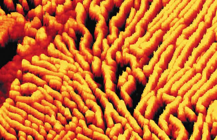
Atomic Force Microscopes
|
|
|
- Candice Reynolds
- 5 years ago
- Views:
Transcription


1 Nanoscale Surface Characterization tomic Force Microscopes

2 WITec tomic Force Microscopes Nanoscale Surface Characterization The WITec tomic Force Microscope (FM) module integrated with a research-grade optical microscope provides superior optical access, easy cantilever tip alignment and highresolution sample survey. The WITec FM objective provides a direct view of both sample and cantilever for straightforward and precise FM tip positioning. ll WITec tomic Force Microscopes are designed for combination with other imaging techniques such as Raman spectroscopy, Scanning Near-field Optical Microscopy (SNOM), luminescence microscopy, polarization analysis and light-field/dark-field illumination. The user can change between imaging methods by simply rotating the (optionally motorized) objective turret. enefits Surface characterization on the nanometer scale Non-destructive imaging Optical and tomic Force Microscope combination Convenient sample access from any direction Minimal, if any, sample preparation Ease of use in air and liquids Combinable with confocal Raman imaging and Scanning Near-field Optical Microscopy (SNOM) TrueScan controlled piezo-driven scanning stages with capacitive feedback loops: - 30 x 30 x 10 µm x 100 x 20 µm x 200 x 20 µm 3 02
 traces the surface contour of living and non-living samples by analyzing the interaction forces")
3 The FM Microscope Laser Photodiode FM Sensor Objectives 02 Piezo-driven scanning stage 03 Koehler white-light illumination 04 Color video camera 05 Z-stage for focusing 06 ctive vibration isolation table Sample Sample Scanning eam Path Working Principle tomic Force Microscopy (FM) traces the surface contour of living and non-living samples by analyzing the interaction forces between the sample s surface and a sharp cantilever tip. The sample is scanned under the tip using a piezo-driven scanning stage and its topography is displayed as an image with up to atomic resolution. The topography of a sample can be acquired while simultaneously extracting other properties such as the sample s adhesion, stiffness, viscosity, electrostatic potential and more. WITec FM 03


 TrueScan corrects the lag errors.")

4 Technology Cantilever Inertial drive cantilever mount for FM sensor positioning ll commercially available FM cantilever tips can be used TrueScan The piezo-driven scanning stage moves the sample forward and reverse during the measurement. The scanning stage s inertia leads to lag errors. This effect increases with scanning speed. While the incorporated capacitive feedback system determines the actual position of the stage, TrueScan can resolve the discrepancy between its actual and intended position, allowing high-resolution lag-free FM imaging at high scanning speeds. Resolution Lateral resolution: Tip radius-dependent, down to 1 nm Depth resolution: Down to atomic scale on silicon, mica, HOPG etc. Computer Interface alphacontrol: Digital controller for WITec microscope systems WITec Control software for instrument and measurement control Data evaluation and processing software included Scan of the straight edge of a sample at speeds between 0.2 s and 1 s per scanning step. () Without TrueScan an increase in scanning speed leads to positioning errors. () TrueScan corrects the lag errors. Simultaneous Cantilever and Sample Viewing for Easy Determination of the Measurement Position 219 nm C The WITec FM objective allows simultaneous sample and cantilever survey from above with high resolution. It facilitates accurate and convenient FM tip alignment and positioning on even very small sample structures. () Simultaneous cantilever and sample viewing. () Overlay of the optical image with the FM image (FM image: C mode, scan range: 3 x 3 μm 2 ). (C) 3D representation of the FM image from. 04


 DPFM allows for the simultaneous acquisition of topography, adhesion, stiffness and other physical properties of the sample. For details see the next section.")
5 FM Modes with DPFM Contact Mode The cantilever tip is kept in contact with the sample surface at a constant bending (force) while it is scanned, revealing the topography of the sample. The bending of the cantilever is monitored with a quadrant photodiode beam-deflection system. In this imaging mode large lateral forces may disturb loosely-bound particles. C Mode In this approach, also called intermittent contact mode, the cantilever oscillates at its resonance frequency and is periodically in contact with the sample. Thus the technique is particularly well suited for delicate samples. When the tip comes close to the surface, sample-tip interaction causes forces to act on the cantilever which alter the phase of its oscillation. This phase shift can be recorded and depicted as a phase image. Lift Mode This mode can be applied in combination with contact mode or C mode. First, the sample is scanned in an imaging mode to trace the surface. Then Lift Mode is used to scan the sample again with a certain z-offset following the previously-recorded topography. Lift Mode is used in combination with EFM, MFM or Kelvin Probe Microscopy to reveal sample properties other than topography. Kelvin Probe Microscopy In this imaging mode the conductive FM tip acts as a vibrating capacitor and measures in Lift Mode TM the differences in surface potential between the tip and the sample. Digital Pulsed Force Mode (DPFM) DPFM allows for the simultaneous acquisition of topography, adhesion, stiffness and other physical properties of the sample. For details see the next section. Magnetic Force Microscopy (MFM) This imaging mode uses a magnetic cantilever scanned in Lift Mode TM over the sample. During the z-offset scan, magnetic properties of the sample are revealed due to the magnetic interaction between the tip and the sample. Electrostatic Force Microscopy (EFM) In this imaging mode electrical properties of a sample surface are imaged. DC voltage is applied between the tip and sample surface while scanning in Lift Mode TM. When the tip is scanned at a z-offset over the sample, electrostatic charges lead to deflections of the cantilever resulting in an electrical properties map of the sample. Nanomanipulation / Lithography The lithography package Da Vinci enables the patterning of material surfaces on the nanometer-scale using tip-sample interaction forces. Lateral Force Microscopy (LFM) This imaging mode uses the twisting of the cantilever while scanning in contact mode to reveal surface friction characteristics. Digital Pulsed Force Mode (DPFM) Pulsed Force Mode (PFM) is a non-resonant, intermittent contact mode for tomic Force Microscopy that allows the characterization of material properties such as adhesion, stiffness and viscosity along with the sample topography. dditionally, lateral forces are virtually eliminated. Therefore high-resolution mapping of delicate samples in air and liquids is easily achievable while maintaining a scanning speed comparable to contact mode FM. In contrast to most other intermittent contact techniques, the perpendicular forces on the sample (introduced by the FM tip) are controlled by the feedback loop. The PFM electronics induce a sinusoidal modulation of the z-piezo of the FM with an amplitude of at a user-selectable frequency of between 100 Hz and 2 khz: far below the resonant frequency of the cantilever. complete force-distance cycle is carried out at this rate, resulting in the force signal as shown in the figure below. Imaging of Surface Properties with DPFM y aseline F max Free Cantilever Oscillation y Force Signal dhesion x Stiffness Force Snap x Stiffness Pulsed Force Mode dhesion Peak Time Viscosity Topography Digital Pulsed Force Mode (DPFM) Contact Time selection of simultaneously-obtained images of a Ethyl-Hexyl-crylate/Polystyrene blend (EH-PS) spin-coated onto a glass substrate. The corresponding curves show the analyzed Pulsed Force Mode properties. Dark areas correspond to low values. Scan range: 10 x 10 µm 2. WITec FM 05

 revealing () topography and ()")

.")

6 pplications Investigation of Electrostatic Characteristics FM images of a gold structure measured in C Lift Mode and with Electric Force Microscopy (EFM) revealing () topography and () conductive/nonconductive areas of the sample. Topography 8 phase High-resolution FM Measurement Image of mono-atomic steps of Highly Ordered Pyrolytic Graphite (HOPG). Sample size: 500 x 30 2, total height in Z: 0.7 nm, height of single steps between layers: 0.3 nm. 0.7 nm 0.3 nm 0.3 nm 06
 250 x 100 µm 2 large-area")


.")

.")


7 Large-area Measurements in Liquids Topography () 250 x 100 µm 2 large-area topography scan of a cell culture in liquid. Maximum measured height: 2.5 µm. () Water immersion objective for FM measurements in liquids. Investigation of Magnetic Forces Topography Magnetic ForCE MICrosCOPY Magnetic Force Microscopy (MFM) measurement of a hard drive. The measurements were performed using C mode with magnetic tips. The topography is flat and uniform (see small image). The MFM image of the same sample area shows a clear magnetic contrast between magnetic hard drive domains (see large image). 4 µm Temperature and Time Series Topography 25 C Topography 90 C Topography 120 C Topography 130 C 4 dhesion 25 C dhesion 90 C dhesion 120 C dhesion 130 C 2.5 nn 0 nn DPFM FM images of heated paraffin at different temperatures. Top row: Topography changes with rising temperature. t 130 C the topography is flattened due to melting processes. Lower row: The adhesion increases while the temperature rises. WITec FM 07


8 Nanomanipulation human chromosome was first cut using the WITec DaVinci nanolithography package and then imaged with FM. The zoom-in highlights the section. < Cut 126 nm pplications of Different FM Modes for Comprehensive Sample Characterization Topography nn 0 nn geological sample including fossilized bacteria was analyzed. adhesion The topography () does not allow the identification of the fossilized organisms. However, measuring the same area in Digital Pulsed Force Mode reveals the presence of the fossils by the difference in adhesion (). 1 µm 08
 imaging demonstrates its most immediate advantage: topography and other physical")

.")


, viscosity (F), tip penetration depth (G) and adhesion energy (H).")

.")
9 Correlative FM and Raman Study of a Polymer lend TOPogrPHY 10 PHSE Digital Pulsed Force Mode (DPFM) imaging demonstrates its most immediate advantage: topography and other physical information can be acquired simultaneously. C E dhesion STIFFNESS 30 nn 10 nn N/m D F Digital Pulsed Force Curves Viscosity mixture containing identical quantities of polystyrene, ethyl-hexyl-acrylate and styrene-butadiene-rubber was spin coated onto glass. The topography of the sample acquired in C mode reveals a threelevel structure (). The simultaneously recorded phase image shows the fine structure of the mixture (). DPFM curves showing the force signal vs. time (D) were recorded from three areas as marked with the corresponding colored crosses in the phase image. For imaging, DPFM curves were measured at each pixel. Differences in the DPFM curves generate contrasts in the images, showing adhesion (C), stiffness (E), viscosity (F), tip penetration depth (G) and adhesion energy (H). G PENETRTION DEPTH 0 N/m 3 1 H dhesion Energy Concurrent with the FM measurements the Raman spectra were recorded at each pixel using the alpha300 R, a combined Raman-FM instrument. Spectral analysis reveals the three components of the blend, here displayed in red = EH, green = PS and blue = mixed spectrum of EH/SR (I). From all data a false color-coded Raman image was generated (J). Correlating FM and Raman images shows that the uppermost and stiffest features of the sample appear to be PS while the thinnest areas contain EH only. I RMN J RMN SPECTR J WITec FM 09


 Height profile of the fiber along the black line in ().")


 FM topography image. (C) 3D representation of FM topography zoom-in image.")
10 FM Study of Collagen Fibers Type I collagen is present in many animal tissues such as bone. It is an elongated, highly organized structure consisting of many long molecules coiled around each other displaying a typical banding pattern. C Mode () C Mode FM phase image of a collagen fiber. () Height profile of the fiber along the black line in (). The profile reveals regular bands 63 nm in width. Simultaneous Raman-FM Measurement Video Image cantilever laser spot lithographed contour 17 nm FM C FM 17 nm Nanolithography in Gas simultaneously imaged by Raman-FM. () Video image with simultaneous cantilever, laser spot and sample view. () FM topography image. (C) 3D representation of FM topography zoom-in image. (D) Raman intensity image. Image parameters: 75 x 75 μm 2 ; 200 x 200 pixels; 0.07 s integration time per spectrum. (E) 3D Raman-FM image overlay. D Raman 10 CCD cts E Raman-FM Overlay 10 CCD cts 0 CCD cts 0 CCD cts 10


 FM topography image (C mode).")

 Raman image of the same area taken and overlaid with the FM image.")

11 Combined Raman-FM Measurement The modular and flexible design of the WITec alpha300 microscope series guarantees easy and cost-effective upgrade and extension possibilities. WITec s product line incorporates nearly all scanning probe and optical microscopy techniques to meet individual requirements. Each WITec alpha300 model can be equipped with new functionalities either as built-in features or as later upgrades. The WITec hardware and software environment is used for all features or upgrades, ensuring the best possible compatibility and ease of use. The objective turret is rotated to change from FM to Raman imaging mode. 2 C Correlative Raman-FM image of exfoliated graphene on a silicon substrate. () Color-coded Raman image showing monolayer (red), bi-layer (blue) and multi-layer (green) graphene. () FM topography image (C mode). (C) Height profile of a cross section along the black line indicated in (). The height variation between one and two layers is approx. 0.3 nm. 1 Correlative Raman-FM study of a CVD-grown graphene layer. () FM topography image, 5 x 5 μm 2. () Raman image of the same area taken and overlaid with the FM image. The different colors indicate layers and wrinkles in the graphene film. 1 compressive C tensile Correlative Raman-FM image of wood extractives. Color-coded Raman image of a cellulose fiber depicting cellulose (green, blue) and hexane extract (red). Inset: High-resolution FM phase image. Correlative Raman-FM measurement investigating stress in silicon via Vickers indent. () 10 x 10 µm 2 FM topography image around a Vickers indent. () FM depth profile view. (C) Corresponding Raman image revealing the areas of stress in silicon. WITec FM 11


 10 6590 0577 Info.China@witec-instruments.com www.witec.de/cn WITec Japan WITec K.")
12 WITec alpha300 Series We take care WITec uses environmentally friendly printed materials. While this policy is only a small contribution to a healthy environment, we at WITec believe that focusing on details can effect positive change in the world. alpha300 R alpha300 alpha300 R alpha300 S WITec Headquarters WITec GmbH Lise-Meitner-Str. 6 D Ulm. Germany Phone +49 (0) Fax +49 (0) info@witec.de WITec North merica WITec Instruments Corp. 130G Market Place lvd. Knoxville. TN US Phone Fax info@witec-instruments.com WITec South East sia WITec Pte. Ltd. 25 International usiness Park #03-59 German Centre Singapore Phone shawn.lee@witec.biz WITec China WITec eijing Representative Office Unit 507, Landmark Tower 1 8 North Dongsanhuan Road eijing, PRC., Phone +86 (0) Info.China@witec-instruments.com WITec Japan WITec K.K. Mita , Chome, Tama-ku, Kawasaki-shi, Kanagawa-ken Japan Phone info@witec-instruments.biz
Microscopic Structures
 Microscopic Structures Image Analysis Metal, 3D Image (Red-Green) The microscopic methods range from dark field / bright field microscopy through polarisation- and inverse microscopy to techniques like
Measurement of Microscopic Three-dimensional Profiles with High Accuracy and Simple Operation
 238 Hitachi Review Vol. 65 (2016), No. 7 Featured Articles Measurement of Microscopic Three-dimensional Profiles with High Accuracy and Simple Operation AFM5500M Scanning Probe Microscope Satoshi Hasumura
INDIAN INSTITUTE OF TECHNOLOGY BOMBAY
 IIT Bombay requests quotations for a high frequency conducting-atomic Force Microscope (c-afm) instrument to be set up as a Central Facility for a wide range of experimental requirements. The instrument
Lateral Force: F L = k L * x
 Scanning Force Microscopy (SFM): Conventional SFM Application: Topography measurements Force: F N = k N * k N Ppring constant: Spring deflection: Pieo Scanner Interaction or force dampening field Contact
WITec alpha300 Series
 Correlative Raman Imaging Raman RISE AFM SNOM WITec alpha300 Series Modular Confocal Raman Microscopy Systems www.witec.de Life Sciences nucleus endoplasmic reticulum nucleoli cytoplasm nuclear membrane
SPM The Industry s Performance Leader High Resolution Closed-loop System Fast, Easy Tip & Sample Exchange Versatility and Value Powerful Research
 SPM The Industry s Performance Leader High Resolution Closed-loop System Fast, Easy Tip & Sample Exchange Versatility and Value Powerful Research Flexibility Atomic resolution STM image of highly-oriented
; A=4π(2m) 1/2 /h. exp (Fowler Nordheim Eq.) 2 const
 1/2 /h. exp (Fowler Nordheim Eq.) 2 const") Scanning Tunneling Microscopy (STM) Brief background: In 1981, G. Binnig, H. Rohrer, Ch. Gerber and J. Weibel observed vacuum tunneling of electrons between a sharp tip and a platinum surface. The tunnel
Scanning Tunneling Microscopy (STM) Brief background: In 1981, G. Binnig, H. Rohrer, Ch. Gerber and J. Weibel observed vacuum tunneling of electrons between a sharp tip and a platinum surface. The tunnel
Cutting-edge Atomic Force Microscopy techniques for large and multiple samples
 Cutting-edge Atomic Force Microscopy techniques for large and multiple samples Study of up to 200 mm samples using the widest set of AFM modes Industrial standards of automation A unique combination of
attosnom I: Topography and Force Images NANOSCOPY APPLICATION NOTE M06 RELATED PRODUCTS G
 APPLICATION NOTE M06 attosnom I: Topography and Force Images Scanning near-field optical microscopy is the outstanding technique to simultaneously measure the topography and the optical contrast of a sample.
Standard Operating Procedure of Atomic Force Microscope (Anasys afm+)
") Standard Operating Procedure of Atomic Force Microscope (Anasys afm+) The Anasys Instruments afm+ system incorporates an Atomic Force Microscope which can scan the sample in the contact mode and generate
Standard Operating Procedure of Atomic Force Microscope (Anasys afm+) The Anasys Instruments afm+ system incorporates an Atomic Force Microscope which can scan the sample in the contact mode and generate
Nanonics Systems are the Only SPMs that Allow for On-line Integration with Standard MicroRaman Geometries
 Nanonics Systems are the Only SPMs that Allow for On-line Integration with Standard MicroRaman Geometries 2002 Photonics Circle of Excellence Award PLC Ltd, England, a premier provider of Raman microspectral
Advanced Nanoscale Metrology with AFM
 Advanced Nanoscale Metrology with AFM Sang-il Park Corp. SPM: the Key to the Nano World Initiated by the invention of STM in 1982. By G. Binnig, H. Rohrer, Ch. Gerber at IBM Zürich. Expanded by the invention
Optical Microscope. Active anti-vibration table. Mechanical Head. Computer and Software. Acoustic/Electrical Shield Enclosure
 Optical Microscope On-axis optical view with max. X magnification Motorized zoom and focus Max Field of view: mm x mm (depends on zoom) Resolution : um Working Distance : mm Magnification : max. X Zoom
Figure for the aim4np Report
 Figure for the aim4np Report This file contains the figures to which reference is made in the text submitted to SESAM. There is one page per figure. At the beginning of the document, there is the front-page
Rebirth of Force Spectroscopy: Advanced Nanomechanical, Electrical, Optical, Thermal and Piezoresponse Studies
 HybriD Mode Rebirth of Force Spectroscopy: Advanced Nanomechanical, Electrical, Optical, Thermal and Piezoresponse Studies Fast Quantitative Nanomechanical Measurements and Force Volume Simultaneous Electrostatic
nanovea.com PROFILOMETERS 3D Non Contact Metrology
 PROFILOMETERS 3D Non Contact Metrology nanovea.com PROFILOMETER INTRO Nanovea 3D Non-Contact Profilometers are designed with leading edge optical pens using superior white light axial chromatism. Nano
attocfm I for Surface Quality Inspection NANOSCOPY APPLICATION NOTE M01 RELATED PRODUCTS G
 APPLICATION NOTE M01 attocfm I for Surface Quality Inspection Confocal microscopes work by scanning a tiny light spot on a sample and by measuring the scattered light in the illuminated volume. First,
NanoFocus Inc. Next Generation Scanning Probe Technology. Tel : Fax:
 NanoFocus Inc. Next Generation Scanning Probe Technology www.nanofocus.kr Tel : 82-2-864-3955 Fax: 82-2-864-3956 Albatross SPM is Multi functional research grade system Flexure scanner and closed-loop
Park NX20 The leading nano metrology tool for failure analysis and large sample research.
 The Most Accurate Atomic Force Microscope Park NX20 The leading nano metrology tool for failure analysis and large sample research www.parkafm.com The Most Accurate Atomic Force Microscope Park NX20 The
Outline: Introduction: What is SPM, history STM AFM Image treatment Advanced SPM techniques Applications in semiconductor research and industry
 1 Outline: Introduction: What is SPM, history STM AFM Image treatment Advanced SPM techniques Applications in semiconductor research and industry 2 Back to our solutions: The main problem: How to get nm
Bringing Answers to the Surface
 3D Bringing Answers to the Surface 1 Expanding the Boundaries of Laser Microscopy Measurements and images you can count on. Every time. LEXT OLS4100 Widely used in quality control, research, and development
Nanosurf easyscan 2 FlexAFM
 Nanosurf easyscan 2 FlexAFM Your Versatile AFM System for Materials and Life Science www.nanosurf.com The new Nanosurf easyscan 2 FlexAFM scan head makes measurements in liquid as simple as measuring in
Distinguishing Between Mechanical and Electrostatic. Interaction in Single-Pass Multifrequency Electrostatic Force
 SUPPORTING INFORMATION Distinguishing Between Mechanical and Electrostatic Interaction in Single-Pass Multifrequency Electrostatic Force Microscopy on a Molecular Material Marta Riba-Moliner, Narcis Avarvari,
Lecture 20: Optical Tools for MEMS Imaging
 MECH 466 Microelectromechanical Systems University of Victoria Dept. of Mechanical Engineering Lecture 20: Optical Tools for MEMS Imaging 1 Overview Optical Microscopes Video Microscopes Scanning Electron
Chemical Imaging. Whiskbroom Imaging. Staring Imaging. Pushbroom Imaging. Whiskbroom. Staring. Pushbroom
 Chemical Imaging Whiskbroom Chemical Imaging (CI) combines different technologies like optical microscopy, digital imaging and molecular spectroscopy in combination with multivariate data analysis methods.
Indian Institute of Technology Bombay
 Specifications for High Resolution Scanning Probe Microscope Item Essential measuring modes with complete hardware and software. All the modes should be demonstrated during installation & training Scanners
Study of shear force as a distance regulation mechanism for scanning near-field optical microscopy
 Study of shear force as a distance regulation mechanism for scanning near-field optical microscopy C. Durkan a) and I. V. Shvets Department of Physics, Trinity College Dublin, Ireland Received 31 May 1995;
- Near Field Scanning Optical Microscopy - Electrostatic Force Microscopy - Magnetic Force Microscopy
 - Near Field Scanning Optical Microscopy - Electrostatic Force Microscopy - Magnetic Force Microscopy Yongho Seo Near-field Photonics Group Leader Wonho Jhe Director School of Physics and Center for Near-field
Atomic Force Microscopy (Bruker MultiMode Nanoscope IIIA)
") Atomic Force Microscopy (Bruker MultiMode Nanoscope IIIA) This operating procedure intends to provide guidance for general measurements with the AFM. For more advanced measurements or measurements with
Atomic Force Microscopy (Bruker MultiMode Nanoscope IIIA) This operating procedure intends to provide guidance for general measurements with the AFM. For more advanced measurements or measurements with
Park XE7 The most affordable research grade AFM with flexible sample handling.
 Park XE7 The most affordable research grade AFM with flexible sample handling www.parkafm.com Park Systems The Most Accurate Atomic Force Microscope Park XE7 The economical choice for innovative research
Akiyama-Probe (A-Probe) guide
 guide") Akiyama-Probe (A-Probe) guide This guide presents: what is Akiyama-Probe, how it works, and what you can do Dynamic mode AFM Version: 2.0 Introduction NANOSENSORS Akiyama-Probe (A-Probe) is a self-sensing
Akiyama-Probe (A-Probe) guide This guide presents: what is Akiyama-Probe, how it works, and what you can do Dynamic mode AFM Version: 2.0 Introduction NANOSENSORS Akiyama-Probe (A-Probe) is a self-sensing
NSOM (SNOM) Overview
 Overview") NSOM (SNOM) Overview The limits of far field imaging In the early 1870s, Ernst Abbe formulated a rigorous criterion for being able to resolve two objects in a light microscope: d > ë / (2sinè) where d
NSOM (SNOM) Overview The limits of far field imaging In the early 1870s, Ernst Abbe formulated a rigorous criterion for being able to resolve two objects in a light microscope: d > ë / (2sinè) where d
MEMS for RF, Micro Optics and Scanning Probe Nanotechnology Applications
 MEMS for RF, Micro Optics and Scanning Probe Nanotechnology Applications Part I: RF Applications Introductions and Motivations What are RF MEMS? Example Devices RFIC RFIC consists of Active components
Park NX-Hivac: Phase-lock Loop for Frequency Modulation Non-Contact AFM
 Park Atomic Force Microscopy Application note #21 www.parkafm.com Hosung Seo, Dan Goo and Gordon Jung, Park Systems Corporation Romain Stomp and James Wei Zurich Instruments Park NX-Hivac: Phase-lock Loop
Akiyama-Probe (A-Probe) guide
 guide") Akiyama-Probe (A-Probe) guide This guide presents: what is Akiyama-Probe, how it works, and its performance. Akiyama-Probe is a patented technology. Version: 2009-03-23 Introduction NANOSENSORS Akiyama-Probe
Akiyama-Probe (A-Probe) guide This guide presents: what is Akiyama-Probe, how it works, and its performance. Akiyama-Probe is a patented technology. Version: 2009-03-23 Introduction NANOSENSORS Akiyama-Probe
Fast Laser Raman Microscope RAMAN
 Fast Laser Raman Microscope RAMAN - 11 www.nanophoton.jp Fast Raman Imaging A New Generation of Raman Microscope RAMAN-11 developed by Nanophoton was created by combining confocal laser microscope technology
Investigate in magnetic micro and nano structures by Magnetic Force Microscopy (MFM)
") Investigate in magnetic micro and nano 5.3.85- Related Topics Magnetic Forces, Magnetic Force Microscopy (MFM), phase contrast imaging, vibration amplitude, resonance shift, force Principle Caution! -
Investigate in magnetic micro and nano 5.3.85- Related Topics Magnetic Forces, Magnetic Force Microscopy (MFM), phase contrast imaging, vibration amplitude, resonance shift, force Principle Caution! -
The Most Accurate Atomic Force Microscope. Park XE15 Power and versatility, brilliantly combined.
 The Most Accurate Atomic Force Microscope Park XE15 Power and versatility, brilliantly combined. www.parkafm.com Park XE15 Increase your productivity with our powerfully versatile atomic force microscope
Basic methods in imaging of micro and nano structures with atomic force microscopy (AFM)
") Basic methods in imaging of micro and nano P2538000 AFM Theory The basic principle of AFM is very simple. The AFM detects the force interaction between a sample and a very tiny tip (
Basic methods in imaging of micro and nano P2538000 AFM Theory The basic principle of AFM is very simple. The AFM detects the force interaction between a sample and a very tiny tip (
Super High Vertical Resolution Non-Contact 3D Surface Profiler BW-S500/BW-D500 Series
 Super High Vertical Resolution Non-Contact 3D Surface Profiler BW-S500/BW-D500 Series Nikon's proprietary scanning-type optical interference measurement technology achieves 1pm* height resolution. * Height
Nanosurf Nanite. Automated AFM for Industry & Research.
 Nanosurf Nanite Automated AFM for Industry & Research www.nanosurf.com Multiple Measurements Automated Got work? Nanosurf has the solution! The Swiss-based innovator and manufacturer of the most compact
3D Optical Motion Analysis of Micro Systems. Heinrich Steger, Polytec GmbH, Waldbronn
 3D Optical Motion Analysis of Micro Systems Heinrich Steger, Polytec GmbH, Waldbronn SEMICON Europe 2012 Outline Needs and Challenges of measuring Micro Structure and MEMS Tools and Applications for optical
Fastest high definition Raman imaging. Fastest Laser Raman Microscope RAMAN
 Fastest high definition Raman imaging Fastest Laser Raman Microscope RAMAN - 11 www.nanophoton.jp Observation A New Generation in Raman Observation RAMAN-11 developed by Nanophoton was newly created by
SENSOR+TEST Conference SENSOR 2009 Proceedings II
 B8.4 Optical 3D Measurement of Micro Structures Ettemeyer, Andreas; Marxer, Michael; Keferstein, Claus NTB Interstaatliche Hochschule für Technik Buchs Werdenbergstr. 4, 8471 Buchs, Switzerland Introduction
IMAGING P-N JUNCTIONS BY SCANNING NEAR-FIELD OPTICAL, ATOMIC FORCE AND ELECTRICAL CONTRAST MICROSCOPY. G. Tallarida Laboratorio MDM-INFM
 Laboratorio MDM - INFM Via C.Olivetti 2, I-20041 Agrate Brianza (MI) M D M Materiali e Dispositivi per la Microelettronica IMAGING P-N JUNCTIONS BY SCANNING NEAR-FIELD OPTICAL, ATOMIC FORCE AND ELECTRICAL
Ionscope SICM. About Ionscope. Scanning Ion Conductance Microscopy. Ionscope A brand of Openiolabs Limited
 SICM About is a brand of openiolabs Ltd, headquartered in Cambridge UK, is the world-leader in (SICM), a rapidly emerging Scanning Probe Microscopy (SPM) technique which allows nanoscale topographical
Electronic Characterization of Materials Using Conductive AFM
 Electronic Characterization of Materials Using Conductive AFM Amir Moshar Electrical Measurements SKPM EFM CAFM PFM SCM Non-Contact Electrical Techniques Scanning Kelvin Probe Microscopy Electric Force
Improving the Collection Efficiency of Raman Scattering
 PERFORMANCE Unparalleled signal-to-noise ratio with diffraction-limited spectral and imaging resolution Deep-cooled CCD with excelon sensor technology Aberration-free optical design for uniform high resolution
The Most Accurate Atomic Force Microscope. Park NX20 The leading nano metrology tool for failure analysis and large sample research.
 The Most Accurate Atomic Force Microscope Park NX20 The leading nano metrology tool for failure analysis and large sample research www.parkafm.com Park Systems The Most Accurate Atomic Force Microscope
Electric polarization properties of single bacteria measured with electrostatic force microscopy
 Electric polarization properties of single bacteria measured with electrostatic force microscopy Theoretical and practical studies of Dielectric constant of single bacteria and smaller elements Daniel
Constant Frequency / Lock-In (AM-AFM) Constant Excitation (FM-AFM) Constant Amplitude (FM-AFM)
 Constant Excitation (FM-AFM) Constant Amplitude (FM-AFM)") HF2PLL Phase-locked Loop Connecting an HF2PLL to a Bruker Icon AFM / Nanoscope V Controller Zurich Instruments Technical Note Keywords: AM-AFM, FM-AFM, AFM control Release date: February 2012 Introduction
HF2PLL Phase-locked Loop Connecting an HF2PLL to a Bruker Icon AFM / Nanoscope V Controller Zurich Instruments Technical Note Keywords: AM-AFM, FM-AFM, AFM control Release date: February 2012 Introduction
Nanoscale Material Characterization with Differential Interferometric Atomic Force Microscopy
 Nanoscale Material Characterization with Differential Interferometric Atomic Force Microscopy F. Sarioglu, M. Liu, K. Vijayraghavan, A. Gellineau, O. Solgaard E. L. Ginzton Laboratory University Tip-sample
Approachable Raman Solutions The Shortest Path from Problem to Answer
 Approachable Raman Solutions The Shortest Path from Problem to Answer Michael S. Bradley The world leader in serving science Thermo Scientific Raman Spectroscopy: Discover. Solve. Assure. Raman Spectroscopy
Fast Laser Raman Microscope RAMAN
 Fast Laser Raman Microscope RAMAN - 11 www.nanophoton.jp Fast Raman Imaging A New Generation of Raman Microscope RAMAN-11 developed by Nanophoton was created by combining confocal laser microscope technology
Prepare Sample 3.1. Place Sample in Stage. Replace Probe (optional) Align Laser 3.2. Probe Approach 3.3. Optimize Feedback 3.4. Scan Sample 3.
 Align Laser 3.2. Probe Approach 3.3. Optimize Feedback 3.4. Scan Sample 3.") CHAPTER 3 Measuring AFM Images Learning to operate an AFM well enough to get an image usually takes a few hours of instruction and practice. It takes 5 to 10 minutes to measure an image if the sample is
CHAPTER 3 Measuring AFM Images Learning to operate an AFM well enough to get an image usually takes a few hours of instruction and practice. It takes 5 to 10 minutes to measure an image if the sample is
Scanning Ion Conductance Microscope ICnano
 Sperm Cell Epithelial Cells I nner Ear Hair Cells I nner Ear Hair Cell Neurons E- Coli Bac teria Scanning Ion Conductance Microscope ICnano About ionscope About ionscope The ionscope scanning ion conductance
SUPPLEMENTARY INFORMATION
 Figure S. Experimental set-up www.nature.com/nature Figure S2. Dependence of ESR frequencies (GHz) on a magnetic field (G) applied in different directions with respect to NV axis ( θ 2π). The angle with
WITec Alpha 300R Quick Operation Summary October 2018
 WITec Alpha 300R Quick Operation Summary October 2018 This document is frequently updated if you feel information should be added, please indicate that to the facility manager (currently Philip Carubia,
Suivie de résonance: méthodes à fréquences multiples. Romain Stomp Application Scientist, Zurich Instruments AG. ZI Applications
 Suivie de résonance: méthodes à fréquences multiples Romain Stomp Application Scientist, Zurich Instruments AG Slide 1 Sommaire 1. Un peu de traitement du signal pour le SPM Détection synchrone pour le
The NanomechPro Toolkit: Accurate Tools for Measuring Nanoscale Mechanical Properties for Diverse Materials
 NanomechPro Toolkit DATA SHEET 43 The NanomechPro Toolkit: Accurate Tools for Measuring Nanoscale Mechanical Properties for Diverse Materials Understanding nanoscale mechanical properties is of fundamental
picoemerald Tunable Two-Color ps Light Source Microscopy & Spectroscopy CARS SRS
 picoemerald Tunable Two-Color ps Light Source Microscopy & Spectroscopy CARS SRS 1 picoemerald Two Colors in One Box Microscopy and Spectroscopy with a Tunable Two-Color Source CARS and SRS microscopy
Using Nanoelectrical Solutions to expand the capability of AFM Dr. Peter De Wolf
 Using Nanoelectrical Solutions to expand the capability of AFM Dr. Peter De Wolf peter.dewolf@bruker.com 2 Atomic Force Microscopy (AFM) Microscopy technique based on raster-scanning and small tipsample
LAB UNIT 1: Introduction Scanning Force Microscopy
 LAB UNIT 1: Introduction Specific Assignment: Setup of scanning force microscopy experiment and first contact measurements Objective Outcome Synopsis The student will become familiar with contact mode
AFM of High-Profile Surfaces
 AFM of High-Profile Surfaces Fig. 1. AFM topograpgy image of black Si made using SCD probe tip. Scan size 4. Profile height is more than 8. See details and other application examples below. High Aspect
A scanning tunneling microscopy based potentiometry technique and its application to the local sensing of the spin Hall effect
 A scanning tunneling microscopy based potentiometry technique and its application to the local sensing of the spin Hall effect Ting Xie 1, a), Michael Dreyer 2, David Bowen 3, Dan Hinkel 3, R. E. Butera
UNIVERSITY OF WATERLOO Physics 360/460 Experiment #2 ATOMIC FORCE MICROSCOPY
 UNIVERSITY OF WATERLOO Physics 360/460 Experiment #2 ATOMIC FORCE MICROSCOPY References: http://virlab.virginia.edu/vl/home.htm (University of Virginia virtual lab. Click on the AFM link) An atomic force
attocube systems Probe Stations for Extreme Environments CRYOGENIC PROBE STATION fundamentals principles of cryogenic probe stations
 PAGE 88 & 2008 2007 PRODUCT CATALOG CRYOGENIC PROBE STATION fundamentals...................... 90 principles of cryogenic probe stations attocps I.......................... 92 ultra stable cryogenic probe
DeltaMyc. Fluorescence Lifetime Mapping Microscope. Affordable Fluorescence Lifetime Imaging Microscopy (FLIM)
") DeltaMyc Fluorescence Lifetime Mapping Microscope Affordable Fluorescence Lifetime Imaging Microscopy (FLIM) DeltaMyc Affordable Fluorescence Imaging Lifetime Microscopy (FLIM) At last, an affordable yet
DeltaMyc Fluorescence Lifetime Mapping Microscope Affordable Fluorescence Lifetime Imaging Microscopy (FLIM) DeltaMyc Affordable Fluorescence Imaging Lifetime Microscopy (FLIM) At last, an affordable yet
_active vibration isolation desktop unit halcyonics_i4 series
 _active vibration isolation desktop unit Active Vibration Isolation Desktop Unit ABSTRACT The halcyonics_i4 is a stateof-the-art active benchtop vibration isolation system from Accurion. Aside from its
Instructions for the Experiment
 Instructions for the Experiment Excitonic States in Atomically Thin Semiconductors 1. Introduction Alongside with electrical measurements, optical measurements are an indispensable tool for the study of
Dynamic Phase-Shifting Microscopy Tracks Living Cells
 from photonics.com: 04/01/2012 http://www.photonics.com/article.aspx?aid=50654 Dynamic Phase-Shifting Microscopy Tracks Living Cells Dr. Katherine Creath, Goldie Goldstein and Mike Zecchino, 4D Technology
A Laser-Based Thin-Film Growth Monitor
 TECHNOLOGY by Charles Taylor, Darryl Barlett, Eric Chason, and Jerry Floro A Laser-Based Thin-Film Growth Monitor The Multi-beam Optical Sensor (MOS) was developed jointly by k-space Associates (Ann Arbor,
Optotop. 3D Topography. Roughness (Ra opt, Rq opt, and Rz opt) Height Distribution. Porosity Distribution. Effective Contact Area
 Height Distribution. Porosity Distribution. Effective Contact Area") Optotop 3D Topography Roughness (Ra opt, Rq opt, and Rz opt) Height Distribution Porosity Distribution Effective Contact Area Basic Functions Highlights Big measurement area up to 60mm x 60mm Easy operation
Optotop 3D Topography Roughness (Ra opt, Rq opt, and Rz opt) Height Distribution Porosity Distribution Effective Contact Area Basic Functions Highlights Big measurement area up to 60mm x 60mm Easy operation
Mapping piezoelectric response in nanomaterials using a dedicated non-destructive scanning probe technique. Supporting Information
 Electronic Supplementary Material (ESI) for Nanoscale. This journal is The Royal Society of Chemistry 2017 Mapping piezoelectric response in nanomaterials using a dedicated non-destructive scanning probe
How are X-ray slides formed?
 P3 Revision. How are X-ray slides formed? X-rays can penetrate soft tissue but not bone. X-rays are absorbed more by some materials than others. Photographic film can be used to detect X-rays, but these
Comparison of resolution specifications for micro- and nanometer measurement techniques
 P4.5 Comparison of resolution specifications for micro- and nanometer measurement techniques Weckenmann/Albert, Tan/Özgür, Shaw/Laura, Zschiegner/Nils Chair Quality Management and Manufacturing Metrology
Electrical Properties of Chicken Herpes Virus Based on Impedance Analysis using Atomic Force Microscopy
 Electrical Properties of Chicken Herpes Virus Based on Impedance Analysis using Atomic Force Microscopy Zhuxin Dong Ph. D. Candidate, Mechanical Engineering University of Arkansas Brock Schulte Masters
pulsecheck The Modular Autocorrelator
 pulsecheck The Modular Autocorrelator Pulse Measurement Perfection with the Multitalent from APE It is good to have plenty of options at hand. Suitable for the characterization of virtually any ultrafast
University of MN, Minnesota Nano Center Standard Operating Procedure
 Equipment Name: Atomic Force Microscope Badger name: afm DI5000 PAN Revisionist Paul Kimani Model: Dimension 5000 Date: October 6, 2017 Location: Bay 1 PAN Revision: 1 A. Description i. Enhanced Motorized
Agilent 8700 LDIR Chemical Imaging System. Bringing Clarity and Unprecedented Speed to Chemical Imaging.
 Agilent 8700 LDIR Chemical Imaging System Bringing Clarity and Unprecedented Speed to Chemical Imaging. What if you could save time and achieve better results? The Agilent 8700 Laser Direct Infrared (LDIR)
Introduction of New Products
 Field Emission Electron Microscope JEM-3100F For evaluation of materials in the fields of nanoscience and nanomaterials science, TEM is required to provide resolution and analytical capabilities that can
Supplementary Materials for
 advances.sciencemag.org/cgi/content/full/2/7/e1629/dc1 Supplementary Materials for Subatomic deformation driven by vertical piezoelectricity from CdS ultrathin films Xuewen Wang, Xuexia He, Hongfei Zhu,
taccor Optional features Overview Turn-key GHz femtosecond laser
 taccor Turn-key GHz femtosecond laser Self-locking and maintaining Stable and robust True hands off turn-key system Wavelength tunable Integrated pump laser Overview The taccor is a unique turn-key femtosecond
Park NX10. The most accurate and easiest to use Atomic Force Microscope.
 The most accurate and easiest to use Atomic Force Microscope www.parkafm.com Park Systems Enabling Nanoscale Advances The premiere choice for nanotechnology research Better data Park NX10 produces data
Add CLUE to your SEM. High-efficiency CL signal-collection. Designed for your SEM and application. Maintains original SEM functionality
 Add CLUE to your SEM Designed for your SEM and application The CLUE family offers dedicated CL systems for imaging and spectroscopic analysis suitable for most SEMs. In addition, when combined with other
PFM Experiments with High Voltage DC/AC Bias
 PFM Experiments with High Voltage DC/AC Bias Support Note Shijie Wu and John Alexander Agilent Technologies Introduction Piezoelectric force microscopy (PFM) has found major applications in the study of
Asylum Research. MFP-3D Infinity. Endless Applications. Unlimited Potential. Performance / Versatility / Support
 MFP-3D Infinity AFM Asylum Research Endless Applications. Unlimited Potential. Performance / Versatility / Support MFP-3D Infinity AFM Asylum Research Endless applications. Unlimited potential. The Asylum
Signal time Signal time FWHM. (~1.5 nm
 ..5..5 -.5 -. -.5 -. 4 6 8..5..5 -.5 -. -.5 -. 4 6 8 E s with singlemode polarization-maintaining fiber s 5nanoM-... 5nanoTE-FI-... 5nanoTE-... 5nanoFI-... Characteristics of s 5nano-...: Coherence length
16. Sensors 217. eye hand control. br-er16-01e.cdr
 16. Sensors 16. Sensors 217 The welding process is exposed to disturbances like misalignment of workpiece, inaccurate preparation, machine and device tolerances, and proess disturbances, Figure 16.1. sensor
Confocal Raman Microscopy (WITec Alpha 300R)
") Confocal Raman Microscopy (WITec Alpha 300R) Please refer to Witec Alpha300R Confocal Raman Microscope User Manual for the details of the operating procedure. Sample preparation 1. Attach your sample on
Confocal Raman Microscopy (WITec Alpha 300R) Please refer to Witec Alpha300R Confocal Raman Microscope User Manual for the details of the operating procedure. Sample preparation 1. Attach your sample on
Imaging Carbon Nanotubes Magdalena Preciado López, David Zahora, Monica Plisch
 Imaging Carbon Nanotubes Magdalena Preciado López, David Zahora, Monica Plisch I. Introduction In this lab you will image your carbon nanotube sample from last week with an atomic force microscope. You
Keysight Technologies Why Magnification is Irrelevant in Modern Scanning Electron Microscopes. Application Note
 Keysight Technologies Why Magnification is Irrelevant in Modern Scanning Electron Microscopes Application Note Introduction From its earliest inception, the Scanning Electron Microscope (SEM) has been
Supporting information: Visualizing the motion of. graphene nanodrums
 Supporting information: Visualizing the motion of graphene nanodrums Dejan Davidovikj,, Jesse J Slim, Santiago J Cartamil-Bueno, Herre S J van der Zant, Peter G Steeneken, and Warner J Venstra,, Kavli
By: Louise Brown, PhD, Advanced Engineered Materials Group, National Physical Laboratory.
 NPL The Olympus LEXT - A highly flexible tool Confocal Metrology at the NPL By: Louise Brown, PhD, Advanced Engineered Materials Group, National Physical Laboratory. www.npl.co.uk louise.brown@npl.co.uk
Spectral phase shaping for high resolution CARS spectroscopy around 3000 cm 1
 Spectral phase shaping for high resolution CARS spectroscopy around 3 cm A.C.W. van Rhijn, S. Postma, J.P. Korterik, J.L. Herek, and H.L. Offerhaus Mesa + Research Institute for Nanotechnology, University
Waveguiding in PMMA photonic crystals
 ROMANIAN JOURNAL OF INFORMATION SCIENCE AND TECHNOLOGY Volume 12, Number 3, 2009, 308 316 Waveguiding in PMMA photonic crystals Daniela DRAGOMAN 1, Adrian DINESCU 2, Raluca MÜLLER2, Cristian KUSKO 2, Alex.
APE Autocorrelator Product Family
 APE Autocorrelator Product Family APE Autocorrelators The autocorrelator product family by APE includes a variety of impressive features and properties, designed to cater for a wide range of ultrafast
Confocal NEXIV VMZ-K Series. CNC Video Measuring System CONFOCAL NEXIV. VMZ-K Series
 Confocal NEXIV VMZ-K Series CNC Video Measuring System CONFOCAL NEXIV VMZ-K Series 3D FOV Measurements Generated with Confocal Images The Confocal NEXIV VMZ-K series, a ground-breaking multifunctional
Surface Finish Measurement Methods and Instrumentation
 125 years of innovation Surface Finish Measurement Methods and Instrumentation Contents Visual Inspection Surface Finish Comparison Plates Contact Gauges Inductive / Variable Reluctance (INTRA) Piezo Electric
Raman images constructed from. Raman Imaging: Defining the Spatial Resolution of the Technology
 18 Raman Technology for Today s Spectroscopists June 26 Raman Imaging: Defining the Spatial Resolution of the Technology Chemical images of polystyrene beads on silicon acquired using Raman mapping and