Optical Waveguides fabricated by combination of ink-jet and flexographic printing
|
|
|
- Augustus Golden
- 5 years ago
- Views:
Transcription
 Institute of Microstructure Technology (IMT) - Karlsruhe Institute of Technology (KIT) 2) Institute of Transport- and Automation Technology (ITA) - University Hanover 3) Department of")
1 Optical Waveguides fabricated by combination of ink-jet and flexographic printing P. Bollgrün 1,3, T. Wolfer 2, U. Gleissner 3 D. Mager 1, C. Megnin 3 T. Hanemann 3,4, L. Overmeyer 2, J. Korvink 1 1) Institute of Microstructure Technology (IMT) - Karlsruhe Institute of Technology (KIT) 2) Institute of Transport- and Automation Technology (ITA) - University Hanover 3) Department of Microsystems Technology (IMTEK) - Universität Freiburg 4) Institute for Applied Materials (IAM) - Karlsruhe Institute of Technology (KIT)
2 Talk Structure 1. Motivation & Research environment 2. Flexo-printed optical waveguides 3. Ink-jet printed optical waveguides 4. Combination of both techniques 5. Next Steps 6. Printing of fluorescent elements - 2 -
3 Motivation and Research Environment - 3 -


4 Research Environment All-optical sensor networks on flexible foil substrates created by additive mass fabrication of polymers T. Wolfer, ITA Hannover - 4 -


5 Applications for Planar Optronic Sensors T. Wolfer, ITA Hannover - 5 -

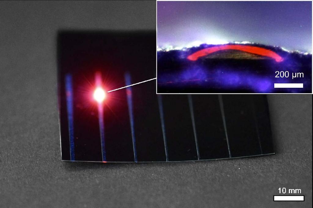
6 Optical Waveguides A high refractive index causes total internal reflection. Light can be confined and guided! PMMA guiding a red laser beam Requirements: Low interface roughness High transparency - 6 -

7 Why Printing? Liquid materials allow effortless creation of optical structures Printing typically aims to cheap mass-production Polymers are established for printing techniques Water on glass = microlenses - 7 -
8 Research Question Can optical waveguides on foils be fabricated by printing techniques? Investigated Techniques: Flexographic printing Ink-jet printing Is a combination of both techniques feasible? - 8 -
9 Flexo-printed optical waveguides - 9 -
 Printed pattern defined by printing plate Ink:")
 Heidelberger Speedmaster SM 52 (Heidelberger")
10 Flexographic Printing (Tim Wolfer, ITA Hannover) High-throughput (1 sheet of 350*500 cm per second) Printed pattern defined by printing plate Ink: Commercial acrylate varnish from Jaenecke- Schneemann Druckfarben) (viscosity: mpas) Heidelberger Speedmaster SM 52 (Heidelberger Druckmaschinen AG)


11 Flexo-printed optical waveguides (Tim Wolfer, ITA Hannover) No pre-treatment, printing at room temperature under normal air Printing Cycles: 10 Post-treatment IR+UV, each layer Confocal microscope scan Width: 100 µm µm Height: 4 µm µm Surface Roughness: 40 nm T. Wolfer, ITA Hannover Attenuation: 0.5 db/cm


12 Optical Characterization Flexo-printed structures Substrate Laser Spot 100 µm 638 nm,140mw Camera at back facet. Integration sphere for power measurement T. Wolfer, ITA Hannover Cutbackmethod to rule out coupling losses
13 Ink-jet printed optical waveguides


14 Ink-jet printed optical waveguides Material: Pre-treatment: InkEpo None Substrate T during Printing: 60 C 75 C for edge pinning Printing Cycles: 20 layers Post-treatment: 60 C for 1h, 2 365nm Width: 75 µm µm Height: 5 µm - 40 µm Confocal microscope scan PMMA Ink Epo 25 µm Surface roughness: <100nm, depending on ink Attenuation: Typically 5 db/cm
15 Combining both methods
16 Combination of Flexo- and Inkjet Possible waveguide concepts by combining the core and cladding layers (Wolfer, ITA Hannover)
17 Combination of Flexo- and Inkjet Core is the new cladding! Ink-jet Flexo Material: Pre-treatment: InkEpo Substrate T during Printing: 60 C Plasma for 60s Printing Cycles: 12 Layers Post-treatment 60 C for 1h, 20 J at 365 nm
18 Ink-jet, n=1.54 Flexo, n=1.516 PMMA, n=


19 31.xx.2010 Forename Surname

20 Waveguide? Ink-jet, n=1.54 Flexo, n=1.516 PMMA, n=

21 Flexo, n=1.516 Ink-jet, n= xx.2010 Forename Surname

22 Flexo, n=1.516 Ink-jet, n= xx.2010 Forename Surname

23 Alternative Method: Edge Pinning! Ink-Jet, n=1.64 Material: UG 164 Pre-treatment Substrate T during Printing Plasma for 60s 60 C Printing Cycles: 24 Layers Post-treatment: 20 J at 365 nm Flexo, n=
24 Attenuation measurement by cut-back 0.6 End Facet Intensity in µw Calculated attenuation 4.9 db/cm Waveguide length in mm
25 Possible Reasons for Attenuation High Attenuation, similar as Ink-jet printing Same diffusion into foil as seen at ink-jet printed waveguides. Explanation for high attenuation Ink-Jet, n=1.64 Flexo, n=
26 Next Steps

27 Combination of Flexo- and Inkjet Class 2? Or Class 3? Next Step Class 3 Waveguide with lower refractive index Possible waveguide concepts by combining the core and cladding layers (Wolfer, ITA, 2014)
28 Research Question Can optical waveguides on foils be fabricated by printing techniques? Investigated Techniques: Flexographic printing Ink-jet printing Yes! (but Ink-jet has high attenuation) Is a combination of both techniques feasible? Not yet
29 Ink-jet printing Available Inks Ink Name Manufacturer Solvent Purpose Comments InkEpo InkOrmo Microresist Technology GBL (Evaporates) Volatile and aggressive solvent UGS70E UG164 Europium-Ink Antracene-Ink IMTEK, Prof Hanemann, Uwe Gleissner EGDMA (Polymerizes) Waveguides Light Emission Scattering dots after polymerisation High refractive index 405 nm 612 nm 365 nm 430 nm
30 Printing of fluorescent elements

31 Fluorescence


32 Fluorescence Fluorescent Element (Ink-jet) Printed Waveguide (Flexo)
33 Fluorescence


34 Thank you for your attention Thanks to for funding
35 Ways to improve Ink-jet attenuation Prevent ink mixing with substrate Polymerize between layers Guide Ink by conditioning lines or grooves in the substrate Switch to chemically more stable substrate like PET
ScienceDirect. Flexographic and inkjet printing of polymer optical waveguides for fully integrated sensor systems
 Available online at www.sciencedirect.com ScienceDirect Procedia Technology 15 (2014 ) 521 529 2nd International Conference on System-Integrated Intelligence: Challenges for Product and Production Engineering
Effect of Corona Treatment on Spreading Behavior of UV Ink over Inkjet Printed Silver Nano-Particle Layer
 Effect of Corona Treatment on Spreading Behavior of UV Ink over Inkjet Printed Silver Nano-Particle Layer Khushbeen Department of Printing Technology GJUS&T, Hisar, Haryana, India Email- khushveen12@gmail.com
Inkjet Filling of TSVs with Silver Nanoparticle Ink. Behnam Khorramdel, Matti Mäntysalo Tampere University of Technology ESTC 2014 Finland, Helsinki
 Inkjet Filling of TSVs with Silver Nanoparticle Ink Behnam Khorramdel, Matti Mäntysalo Tampere University of Technology ESTC 2014 Finland, Helsinki Outline Motivation for this study Inkjet in MEMS fabrication
Zukunftstechnologie Dünnglasbasierte elektrooptische. Research Center of Microperipheric Technologies
 Zukunftstechnologie Dünnglasbasierte elektrooptische Baugruppenträger Dr. Henning Schröder Fraunhofer IZM, Berlin, Germany Today/Overview Motivation: external roadmaps High Bandwidth and Channel Density
Femtosecond laser microfabrication in. Prof. Dr. Cleber R. Mendonca
 Femtosecond laser microfabrication in polymers Prof. Dr. Cleber R. Mendonca laser microfabrication focus laser beam on material s surface laser microfabrication laser microfabrication laser microfabrication
A BASIC EXPERIMENTAL STUDY OF CAST FILM EXTRUSION PROCESS FOR FABRICATION OF PLASTIC MICROLENS ARRAY DEVICE
 A BASIC EXPERIMENTAL STUDY OF CAST FILM EXTRUSION PROCESS FOR FABRICATION OF PLASTIC MICROLENS ARRAY DEVICE Chih-Yuan Chang and Yi-Min Hsieh and Xuan-Hao Hsu Department of Mold and Die Engineering, National
Examination Optoelectronic Communication Technology. April 11, Name: Student ID number: OCT1 1: OCT 2: OCT 3: OCT 4: Total: Grade:
 Examination Optoelectronic Communication Technology April, 26 Name: Student ID number: OCT : OCT 2: OCT 3: OCT 4: Total: Grade: Declaration of Consent I hereby agree to have my exam results published on
 Chapter 5 5.1 What are the factors that determine the thickness of a polystyrene waveguide formed by spinning a solution of dissolved polystyrene onto a substrate? density of polymer concentration of polymer
Contents. Contents. Preface... xi. PART A: OVERVIEW 1 Introduction... 1
 Contents Preface... xi PART A: OVERVIEW 1 Introduction... 1 1.1 Scope...1 1.2 Innovation and Patents...1 1.3 Prediction of Trends...1 1.4 Innovators...2 1.5 Comments on Presentation...3 1.5.1 Subject Classification...3
OPTI510R: Photonics. Khanh Kieu College of Optical Sciences, University of Arizona Meinel building R.626
 OPTI510R: Photonics Khanh Kieu College of Optical Sciences, University of Arizona kkieu@optics.arizona.edu Meinel building R.626 Announcements Homework #3 is due today No class Monday, Feb 26 Pre-record
Bringing Answers to the Surface
 3D Bringing Answers to the Surface 1 Expanding the Boundaries of Laser Microscopy Measurements and images you can count on. Every time. LEXT OLS4100 Widely used in quality control, research, and development
Capacitive Sensors Realized on Flexible Substrates
 Ročník 2017 Číslo II Capacitive Sensors Realized on Flexible Substrates S. Zuk 1, A. Pietrikova 1 1 Department of Technologies in Electronics, Faculty of Electrical Engineering and Informatics, Technical
Micro- and Nano-Technology... for Optics
 Micro- and Nano-Technology...... for Optics 3.2 Lithography U.D. Zeitner Fraunhofer Institut für Angewandte Optik und Feinmechanik Jena Printing on Stones Map of Munich Stone Print Contact Printing light
Lab-level and low-cost fabrication technique for polymer based micro-optical elements and holographic structures
 Lab-level and low-cost fabrication technique for polymer based micro-optical elements and holographic structures Maik Rahlves a, Maher Rezem a, Christian Kelb a, Kristian Boroz a, Dina Gödeke a, Sebastian
Lecture 22 Optical MEMS (4)
") EEL6935 Advanced MEMS (Spring 2005) Instructor: Dr. Huikai Xie Lecture 22 Optical MEMS (4) Agenda: Refractive Optical Elements Microlenses GRIN Lenses Microprisms Reference: S. Sinzinger and J. Jahns,
EEL6935 Advanced MEMS (Spring 2005) Instructor: Dr. Huikai Xie Lecture 22 Optical MEMS (4) Agenda: Refractive Optical Elements Microlenses GRIN Lenses Microprisms Reference: S. Sinzinger and J. Jahns,
Integrated electro-optical waveguide based devices with liquid crystals on a silicon backplane
 Integrated electro-optical waveguide based devices with liquid crystals on a silicon backplane Florenta Costache Group manager Smart Micro-Optics SMO/AMS Fraunhofer Institute for Photonic Microsystems,
Polymer Optical Waveguide Fabrication Using Laser Ablation
 Polymer Optical Waveguide Fabrication Using Laser Ablation Shefiu Zakariyah Loughborough University Shefiu S. Zakariyah, Paul P. Conway, David A. Hutt, #David R. Selviah, #Kai Wang #Hadi Baghsiahi *Jeremy
Just where it s needed
 Seite/Page: 1 Just where it s needed Continuing miniaturisation of many products requires a method of dispensing very small amounts of liquids Inkjet technology is capable of applying adhesives and many
Photonics and Optical Communication Spring 2005
 Photonics and Optical Communication Spring 2005 Final Exam Instructor: Dr. Dietmar Knipp, Assistant Professor of Electrical Engineering Name: Mat. -Nr.: Guidelines: Duration of the Final Exam: 2 hour You
Fabrication of Silicon Master Using Dry and Wet Etching for Optical Waveguide by Thermal Embossing Technique
 Sensors and Materials, Vol. 18, No. 3 (2006) 125 130 MYU Tokyo 125 S & M 0636 Fabrication of Silicon Master Using Dry and Wet Etching for Optical Waveguide by Thermal Embossing Technique Jung-Hun Kim,
3D and Aerosol Printed Conductor Dielectric Full- 3D RF Metamaterials
 3D and Aerosol Printed Conductor Dielectric Full- 3D RF Metamaterials June 22, 2017 Jimmy Hester, Evan Nguyen, Jesse Tice, and Vesna Radisic Approved for Public Release: NG17-1180, 6/2/17 Outline Introduction
INTEGRATED OPTICAL AND ELECTRONIC INTERCONNECT PCB MANUFACTURING (OPCB)
") INTEGRATED OPTICAL AND ELECTRONIC INTERCONNECT PCB MANUFACTURING (OPCB) IeMRC FLAGSHIP PROJECT IeMRC Annual Conference Loughborough 4 th July 2008 PROJECT OBJECTIVES 1. Enhance fabrication techniques for
INTEGRATED OPTICAL AND ELECTRONIC INTERCONNECT PCB MANUFACTURING (OPCB) IeMRC FLAGSHIP PROJECT IeMRC Annual Conference Loughborough 4 th July 2008 PROJECT OBJECTIVES 1. Enhance fabrication techniques for
Laser Ablation and Laser Direct Writing as Enabling Technologies for the Definition of Micro-Optical Elements
 Laser Ablation and Laser Direct Writing as Enabling Technologies for the Definition of Micro-Optical Elements Nina Hendrickx *1, Himanshu Suyal 2, Geert Van Steenberge 1, Aongus McCarthy 2, Andy Walker
CHARACTERISATION OF ADAPTIVE FLUIDIC SILICONE- MEMBRANE LENSES
 CHARACTERISATION OF ADAPTIVE FLUIDIC SILICONE- MEMBRANE LENSES F. Schneider 1,2,J. Draheim 2, J. Brunne 2, P. Waibel 2 and U. Wallrabe 2 1 Material Science and Manufacturing, CSIR, PO Box 395, Pretoria,
WDM board-level optical communications
 MIT Microphotonics Center Spring Meeting, May 22 nd WDM board-level optical communications Jürgen Schrage Siemens AG,, Germany Outline Introduction to board-level optical communications, WDM motivation
OPTICAL FIBRE SENSOR FOR MONITORING FLOW AND RESIN CURING IN COMPOSITES MANUFACTURING
 OPTICAL FIBRE SENSOR FOR MONITORING FLOW AND RESIN CURING IN COMPOSITES MANUFACTURING C.Lekakou *, S.Cook *, Y.Deng *, T.W.Ang ** and G.T.Reed ** * School of Engineering ** School of Electronics, Computing
Part 5-1: Lithography
 Part 5-1: Lithography Yao-Joe Yang 1 Pattern Transfer (Patterning) Types of lithography systems: Optical X-ray electron beam writer (non-traditional, no masks) Two-dimensional pattern transfer: limited
4-Channel Optical Parallel Transceiver. Using 3-D Polymer Waveguide
 4-Channel Optical Parallel Transceiver Using 3-D Polymer Waveguide 1 Description Fujitsu Component Limited, in cooperation with Fujitsu Laboratories Ltd., has developed a new bi-directional 4-channel optical
Supplementary Information for. Surface Waves. Angelo Angelini, Elsie Barakat, Peter Munzert, Luca Boarino, Natascia De Leo,
 Supplementary Information for Focusing and Extraction of Light mediated by Bloch Surface Waves Angelo Angelini, Elsie Barakat, Peter Munzert, Luca Boarino, Natascia De Leo, Emanuele Enrico, Fabrizio Giorgis,
Fabrication methods for SU-8 optical interconnects in plastic substrates
 Fabrication methods for SU-8 optical interconnects in plastic substrates Author Hamid, Hanan, Fickenscher, Thomas, O'Keefe, Steven, Thiel, David Published 2014 Journal Title Photonics Technology Letters
ML² Multi Layer Micro Lab
 Deliverable 4.5 ML² Multi Layer Micro Lab D4.5 - Report on product range for UV curing lacquers, validated for ML² devices 1. Introduction... 2 2. UV embossing lacquer chemistry... 2 2.1. The main components
attocfm I for Surface Quality Inspection NANOSCOPY APPLICATION NOTE M01 RELATED PRODUCTS G
 APPLICATION NOTE M01 attocfm I for Surface Quality Inspection Confocal microscopes work by scanning a tiny light spot on a sample and by measuring the scattered light in the illuminated volume. First,
Towards a fully integrated optical gyroscope using whispering gallery modes resonators
 Towards a fully integrated optical gyroscope using whispering gallery modes resonators T. Amrane 1, J.-B. Jager 2, T. Jager 1, V. Calvo 2, J.-M. Leger 1 1 CEA, LETI, Grenoble, France. 2 CEA, INAC-SP2M
ORGANIC ELECTRONICS: PHOTOLITHOGRAPHY OR PRINTING. Giles Lloyd Flex Europe Conference, 25th October 2016
 ORGANIC ELECTRONICS: PHOTOLITHOGRAPHY OR PRINTING Giles Lloyd Flex Europe Conference, 25th October 2016 Organic Electronics: Photoligthography or Printing? Lithography Printing Enabling flexible TFT sheet-fed
Optical fibre. Principle and applications
 Optical fibre Principle and applications Circa 2500 B.C. Earliest known glass Roman times-glass drawn into fibers Venice Decorative Flowers made of glass fibers 1609-Galileo uses optical telescope 1626-Snell
Drop-on-Demand Inkjet Printing of Liquid Crystals for Photonics Applications
 Drop-on-Demand Inkjet Printing of Liquid Crystals for Photonics Applications Ellis Parry, Steve Elston, Alfonson Castrejon-Pita, Serena Bolis and Stephen Morris PhD Student University of Oxford Drop-on
Microprobe-enabled Terahertz sensing applications
 Microprobe-enabled Terahertz sensing applications World of Photonics, Laser 2015, Munich Protemics GmbH Aachen, Germany Terahertz microprobing technology: Taking advantage of Terahertz range benefits without
EUV Substrate and Blank Inspection
 EUV Substrate and Blank Inspection SEMATECH EUV Workshop 10/11/99 Steve Biellak KLA-Tencor RAPID Division *This work is partially funded by NIST-ATP project 98-06, Project Manager Purabi Mazumdar 1 EUV
Beam Shaping and Simultaneous Exposure by Diffractive Optical Element in Laser Plastic Welding
 Beam Shaping and Simultaneous Exposure by Diffractive Optical Element in Laser Plastic Welding AKL`12 9th May 2012 Dr. Daniel Vogler Page 1 Motivation: Quality and flexibility diffractive spot shaping
Technical Information 50.G.003 Radiation-curing Systems General Information, Services
 Technical Information 50.G.003 Radiation-curing Systems General Information, Services NewV UV curing inks and varnishes for flexo printing Direction for use NewV flex_direction for use 06/2017 en TABLE
Multicolor Production Printing Using Computer to Plate Technologies
 Multicolor Production Printing Using Computer to Plate Technologies Martin Schmitt-Lewen Heidelberger Druckmaschinen AG Heidelberg, Germany Abstract Conventional printing technologies for high quality
3D flow focusing chips
 Unit 1, Anglian Business Park, Orchard Road, Royston, Hertfordshire, SG8 5TW, UK T: +44 (0)1763 242491 F: +44 (0)1763 246125 E: sales@dolomite-microfluidics.com W: www.dolomite-microfluidics.com Dolomite
Graded-Index Core Polymer Optical Waveguide for High-bandwidth-density On-Board Interconnect
 European Cluster for Optical Interconnects (ECO) Workshop Sep. 25, 2013 Graded-Index Core Polymer Optical Waveguide for High-bandwidth-density On-Board Interconnect Takaaki Ishigure Faculty of Science
Laser Scanning for Surface Analysis of Transparent Samples - An Experimental Feasibility Study
 STR/03/044/PM Laser Scanning for Surface Analysis of Transparent Samples - An Experimental Feasibility Study E. Lea Abstract An experimental investigation of a surface analysis method has been carried
Flexible Packaging Printing Processes Overview
 for Barrier Performance Course Flexible Packaging Printing Processes Overview Presented by: Warren E. Durling Associate Research Fellow The Clorox Company (GLAD) Flexible Packaging Printing Processes Overview
PHGN/CHEN/MLGN 435/535: Interdisciplinary Silicon Processing Laboratory. Simple Si solar Cell!
 Where were we? Simple Si solar Cell! Two Levels of Masks - photoresist, alignment Etch and oxidation to isolate thermal oxide, deposited oxide, wet etching, dry etching, isolation schemes Doping - diffusion/ion
NOVEL APPLICATIONS OF CONFOCAL MICROSCOPY TECHNIQUES IN COATINGS RESEARCH
 ARKEMA COATING RESINS NOVEL APPLICATIONS OF CONFOCAL MICROSCOPY TECHNIQUES IN COATINGS RESEARCH DOUG MALL FOR DR. WENJUN WU 9/20/2018 Wood Coatings & Substrates Conference 2018 OUTLINE Introduction Confocal
Flexible Glass Applications & Process Scaling
 Flexible Glass Applications & Process Scaling Sean Garner, Sue Lewis, Gary Merz, Alex Cuno, Ilia Nikulin October 16, 2017 Outline Flexible Glass Applications Process Scaling Summary 2 Flexible Glass Enables
ENERGY SCIENCES INC. EB COATING DEVELOPMENTS FOR GRAPHIC ARTS
 ENERGY SCIENCES INC. EB COATING DEVELOPMENTS FOR GRAPHIC ARTS WHAT IS EB? INNOVATIVE METHOD OF IMMEDIATELY DRYING INKS COATINGS ADHESIVES WITHOUT HEAT OR LIGHT. HOW DOES AN E-BEAM WORK? Ø FILAMENTS EMIT
Inkjet resist inks. Krishna Balantrapu
 Inkjet resist inks Krishna Balantrapu OUTLINE Conventional Vs. Inkjet-Cost Savings Inkjet Material Design Inkjet Equipment-Lunaris Future work 2 DOW-R&D DRIVERS FOR NEW PRODUCT DEVELOPMENT Technology Need
Design, Fabrication and Characterization of Very Small Aperture Lasers
 372 Progress In Electromagnetics Research Symposium 2005, Hangzhou, China, August 22-26 Design, Fabrication and Characterization of Very Small Aperture Lasers Jiying Xu, Jia Wang, and Qian Tian Tsinghua
Optical planar multimode 1x2Y splitters
 POSTER 017, PRAGUE MAY 3 1 Optical planar multimode 1xY splitters Marian KNIETEL 1 1 Dept. o Microelectronics, Czech Technical University, Technická, 166 7 Prague, Czech Republic knietmar@el.cvut.cz Abstract.
Figure 7 Dynamic range expansion of Shack- Hartmann sensor using a spatial-light modulator
 Figure 4 Advantage of having smaller focal spot on CCD with super-fine pixels: Larger focal point compromises the sensitivity, spatial resolution, and accuracy. Figure 1 Typical microlens array for Shack-Hartmann
Fabrication of PDMS (polydimethylsiloxane) microlens and diffuser using replica molding
 microlens and diffuser using replica molding") From the SelectedWorks of Fang-Tzu Chuang Summer June 22, 2006 Fabrication of PDMS (polydimethylsiloxane) microlens and diffuser using replica molding Fang-Tzu Chuang Available at: https://works.bepress.com/ft_chuang/4/
From the SelectedWorks of Fang-Tzu Chuang Summer June 22, 2006 Fabrication of PDMS (polydimethylsiloxane) microlens and diffuser using replica molding Fang-Tzu Chuang Available at: https://works.bepress.com/ft_chuang/4/
Hermetic Packaging Solutions using Borosilicate Glass Thin Films. Lithoglas Hermetic Packaging Solutions using Borosilicate Glass Thin Films
 Hermetic Packaging Solutions using Borosilicate Glass Thin Films 1 Company Profile Company founded in 2006 ISO 9001:2008 qualified since 2011 Headquarters and Production in Dresden, Germany Production
Fabrication of adhesive lenses using free surface shaping
 J. Europ. Opt. Soc. Rap. Public. 8, 13065 (2013) www.jeos.org Fabrication of adhesive lenses using free surface shaping D. Hoheisel hoheisel@impt.uni-hannover.de Leibniz Universität Hannover, Center for
EXAM NYC-05 Waves, optics and modern physics
 EXAM 2 203-NYC-05 Waves, optics and modern physics Fall 2017 Prof: Jean-Raphaël Carrier Name: Instructions For questions 1 to 10, only the correct answer(s) is(are) needed. For questions 11 to 14, clearly
First Demonstration of Single-mode Polymer Optical Waveguides with Circular Cores for Fiber-to-waveguide Coupling in 3D Glass Photonic Interposers
 First Demonstration of Single-mode Polymer Optical Waveguides with Circular Cores for Fiber-to-waveguide Coupling in 3D Glass Photonic Interposers Rui Zhang^, Fuhan Liu, Venky Sundaram, and Rao Tummala
Laser printing for micro and nanomanufacturing
 Laser printing for micro and nanomanufacturing Ph. Delaporte Lasers, Plasmas and Photonics Processes Laboratory, CNRS, Aix-Marseille University Marseille, France Contact: Philippe Delaporte delaporte@lp3.univ-mrs.fr
Optical Characterization of Compound Refractive Lenses
 Optical Characterization of Compound Refractive Lenses ARNDT LAST, INSTITUTE OF MICROSTRUCTURE TECHNOLOGY (IMT) CRL Layout 1357_00_A0 KIT University of the State of Baden-Wuerttemberg and National Research
Numerical Method Approaches in Optical Waveguide Modeling
 Applied Mechanics and Materials Vols. 52-54 (2011) pp 2133-2137 Online available since 2011/Mar/28 at www.scientific.net (2011) Trans Tech Publications, Switzerland doi:10.4028/www.scientific.net/amm.52-54.2133
Pulsed Laser Power Measurement Systems
 Pulsed Laser Power Measurement Systems Accurate, reproducible method of determining total laser and laser diode power Ideal for Beam Power Measurement Labsphere s Pulsed Laser Power Measurement Systems
Optical Microscopy and Imaging ( Part 2 )
") 1 Optical Microscopy and Imaging ( Part 2 ) Chapter 7.1 : Semiconductor Science by Tudor E. Jenkins Saroj Kumar Patra, Department of Electronics and Telecommunication, Norwegian University of Science and
1 Optical Microscopy and Imaging ( Part 2 ) Chapter 7.1 : Semiconductor Science by Tudor E. Jenkins Saroj Kumar Patra, Department of Electronics and Telecommunication, Norwegian University of Science and
Outline. 1 Introduction. 2 Basic IC fabrication processes. 3 Fabrication techniques for MEMS. 4 Applications. 5 Mechanics issues on MEMS MDL NTHU
 Outline 1 Introduction 2 Basic IC fabrication processes 3 Fabrication techniques for MEMS 4 Applications 5 Mechanics issues on MEMS 2.2 Lithography Reading: Runyan Chap. 5, or 莊達人 Chap. 7, or Wolf and
SURFACE ANALYSIS STUDY OF LASER MARKING OF ALUMINUM
 SURFACE ANALYSIS STUDY OF LASER MARKING OF ALUMINUM Julie Maltais 1, Vincent Brochu 1, Clément Frayssinous 2, Réal Vallée 3, Xavier Godmaire 4 and Alex Fraser 5 1. Summer intern 4. President 5. Chief technology
Enhanced reproducibility of inkjet printed organic thin film transistors based on solution processable polymer-small molecule blends.
 Enhanced reproducibility of inkjet printed organic thin film transistors based on solution processable polymer-small molecule blends. Marie-Beatrice Madec 1*, Patrick J. Smith 2, Andromachi Malandraki
Via Carolina Romani 1/11 I Bresso (MI) Italy Tel Fax
 Italy Tel Fax") Italian Polyurethane Manufacturer Via Carolina Romani 1/11 I-20091 Bresso (MI) Italy Tel. 0039+02+6103166 Fax 0039+02+6105708 E-mail: sintochem@sintochem.it Web-site: www.sintochem.com The company SINTOCHEM
Italian Polyurethane Manufacturer Via Carolina Romani 1/11 I-20091 Bresso (MI) Italy Tel. 0039+02+6103166 Fax 0039+02+6105708 E-mail: sintochem@sintochem.it Web-site: www.sintochem.com The company SINTOCHEM
Exp. No. 13 Measuring the runtime of light in the fiber
 Exp. No. 13 Measuring the runtime of light in the fiber Aim of Experiment The aim of experiment is measuring the runtime of light in optical fiber with length of 1 km and the refractive index of optical
SUPPLEMENTARY INFORMATION
 Room-temperature continuous-wave electrically injected InGaN-based laser directly grown on Si Authors: Yi Sun 1,2, Kun Zhou 1, Qian Sun 1 *, Jianping Liu 1, Meixin Feng 1, Zengcheng Li 1, Yu Zhou 1, Liqun
On-chip Si-based Bragg cladding waveguide with high index contrast bilayers
 On-chip Si-based Bragg cladding waveguide with high index contrast bilayers Yasha Yi, Shoji Akiyama, Peter Bermel, Xiaoman Duan, and L. C. Kimerling Massachusetts Institute of Technology, 77 Massachusetts
Spot Colour Printing an explanation
 Let me show you how it works the offset litho printing and at the same time the digital colour printing: Spot Colour Printing an explanation Spot colour is for when you wish to have just one or two colours
DEVELOPMENT PROCESS FOR PVCz HOLOGRAM
 Journal of Photopolymer Science and Technology Volume 4, Number 1(1991) 127-134 DEVELOPMENT PROCESS FOR PVCz HOLOGRAM Yasuo YAMAGISHI, Takeshi ISHITSUKA, and Yasuhiro YONEDA Fujitsu Laboratories Ltd. Morinosato
Effect of paper properties on print quality by flexographic method
 Effect of paper properties on print quality by flexographic method Stamatina Theohari 1, Eftihis Fraggedakis 1, Diana Tsimis 1, Marios Tsigonias 1 and Dimitris Mandis 2 1 Graphic rts Technology Department,
High-Resolution Bubble Printing of Quantum Dots
 SUPPORTING INFORMATION High-Resolution Bubble Printing of Quantum Dots Bharath Bangalore Rajeeva 1, Linhan Lin 1, Evan P. Perillo 2, Xiaolei Peng 1, William W. Yu 3, Andrew K. Dunn 2, Yuebing Zheng 1,*
High-Accuracy Surface Scanning Method
 Surface Scanning Laser Confocal Displacement Meter LT-9000 Series First in the world High-Accuracy Surface Scanning Method High resolution of 0.3 µm The high-accuracy, surface scanning method allows measurements
Integrated Focusing Photoresist Microlenses on AlGaAs Top-Emitting VCSELs
 Integrated Focusing Photoresist Microlenses on AlGaAs Top-Emitting VCSELs Andrea Kroner We present 85 nm wavelength top-emitting vertical-cavity surface-emitting lasers (VCSELs) with integrated photoresist
ScanArray Overview. Principle of Operation. Instrument Components
 ScanArray Overview The GSI Lumonics ScanArrayÒ Microarray Analysis System is a scanning laser confocal fluorescence microscope that is used to determine the fluorescence intensity of a two-dimensional
Technical Explanation for Displacement Sensors and Measurement Sensors
 Technical Explanation for Sensors and Measurement Sensors CSM_e_LineWidth_TG_E_2_1 Introduction What Is a Sensor? A Sensor is a device that measures the distance between the sensor and an object by detecting
An Optical Characteristic Testing System for the Infrared Fiber in a Transmission Bandwidth 9-11μm
 An Optical Characteristic Testing System for the Infrared Fiber in a Transmission Bandwidth 9-11μm Ma Yangwu *, Liang Di ** Center for Optical and Electromagnetic Research, State Key Lab of Modern Optical
Resolution. Diffraction from apertures limits resolution. Rayleigh criterion θ Rayleigh = 1.22 λ/d 1 peak at 2 nd minimum. θ f D
 Microscopy Outline 1. Resolution and Simple Optical Microscope 2. Contrast enhancement: Dark field, Fluorescence (Chelsea & Peter), Phase Contrast, DIC 3. Newer Methods: Scanning Tunneling microscopy (STM),
Advanced 3D Optical Profiler using Grasshopper3 USB3 Vision camera
 Advanced 3D Optical Profiler using Grasshopper3 USB3 Vision camera Figure 1. The Zeta-20 uses the Grasshopper3 and produces true color 3D optical images with multi mode optics technology 3D optical profiling
Waveguiding in PMMA photonic crystals
 ROMANIAN JOURNAL OF INFORMATION SCIENCE AND TECHNOLOGY Volume 12, Number 3, 2009, 308 316 Waveguiding in PMMA photonic crystals Daniela DRAGOMAN 1, Adrian DINESCU 2, Raluca MÜLLER2, Cristian KUSKO 2, Alex.
plasmonic nanoblock pair
 Nanostructured potential of optical trapping using a plasmonic nanoblock pair Yoshito Tanaka, Shogo Kaneda and Keiji Sasaki* Research Institute for Electronic Science, Hokkaido University, Sapporo 1-2,
Fabrication Techniques of Optical ICs
 Fabrication Techniques of Optical ICs Processing Techniques Lift off Process Etching Process Patterning Techniques Photo Lithography Electron Beam Lithography Photo Resist ( Microposit MP1300) Electron
Section 2: Lithography. Jaeger Chapter 2. EE143 Ali Javey Slide 5-1
 Section 2: Lithography Jaeger Chapter 2 EE143 Ali Javey Slide 5-1 The lithographic process EE143 Ali Javey Slide 5-2 Photolithographic Process (a) (b) (c) (d) (e) (f) (g) Substrate covered with silicon
Photolithography Technology and Application
 Photolithography Technology and Application Jeff Tsai Director, Graduate Institute of Electro-Optical Engineering Tatung University Art or Science? Lind width = 100 to 5 micron meter!! Resolution = ~ 3
<Chap. 2 Optics> 1.Light directivity. Light directivity can be seen using smoke and milky water in a plastic bottle
 1.Light directivity Light directivity can be seen using smoke and milky water in a plastic bottle Laser 3 cm Principle of pinhole camera (γray camera) Object Dark image Eye Ground glass
Examination, TEN1, in courses SK2500/SK2501, Physics of Biomedical Microscopy,
 KTH Applied Physics Examination, TEN1, in courses SK2500/SK2501, Physics of Biomedical Microscopy, 2009-06-05, 8-13, FB51 Allowed aids: Compendium Imaging Physics (handed out) Compendium Light Microscopy
PHOTOPOLYMER FOR RECORDING HOLOGRAMS. Hideo Tanigawa, Taichi Ichihashi, and Takashi Matsuo*
 PHOTOPOLYMER FOR RECORDING HOLOGRAMS Hideo Tanigawa, Taichi Ichihashi, and Takashi Matsuo* MY0001406 Osaka National Research Institute, AIST 1-8-31, Midorigaoka, Ikeda, Osaka 563-8577, Japan Phone: +81-727-51-9537,
Organic Optical Waveguide Fabrication in a Manufacturing Environment
 Organic Optical Waveguide Fabrication in a Manufacturing Environment Benson Chan, How Lin, Chase Carver, Jianzhuang Huang, Jessie Berry Endicott Interconnect Technologies 1093 Clark Street, Endicott NY
DISPERSION COMPENSATING FIBER
 DISPERSION COMPENSATING FIBER Dispersion-Compensating SM Fiber for Telecom Wavelengths (1520-1625 nm) DCF38 is Specifically Designed to Compensate Corning SMF-28e+ Fiber Short Pulse Broad Pulse due to
Propagation loss study of very compact GaAs/AlGaAs substrate removed waveguides
 Propagation loss study of very compact GaAs/AlGaAs substrate removed waveguides JaeHyuk Shin, Yu-Chia Chang and Nadir Dagli * Electrical and Computer Engineering Department, University of California at
Unique and sustainable surface refinement of products with innovative thin films: Ara Authentic. R. Domnick, Ara-Authentic GmbH
 Unique and sustainable surface refinement of products with innovative thin films: Ara Authentic R. Domnick, Ara-Authentic GmbH 1 Introduction - About us - Piracy of products a growing problem - Protection
Optics Communications
 Optics Communications 283 (2010) 3678 3682 Contents lists available at ScienceDirect Optics Communications journal homepage: www.elsevier.com/locate/optcom Ultra-low-loss inverted taper coupler for silicon-on-insulator
Horizontal single and multiple slot waveguides: optical transmission at λ = 1550 nm
 Horizontal single and multiple slot waveguides: optical transmission at λ = 1550 nm Rong Sun 1 *, Po Dong 2 *, Ning-ning Feng 1, Ching-yin Hong 1, Jurgen Michel 1, Michal Lipson 2, Lionel Kimerling 1 1Department
CERIDUST. Micronized Wax for Printing Inks. Public. BU Additives BL Waxes Technical Marketing Formulators/Coatings&Inks
 CERIDUST Micronized Wax for Printing Inks Public BU Additives BL Waxes Technical Marketing Formulators/Coatings&Inks 27.11.2014 2 Table of Contents Introduction Which effects are provided by CERIDUST in
Paper Parameters That Affect Color Reproduction. Danny C. Rich, Ph.D. Sun Chemical Color Research Laboratory
 Paper Parameters That Affect Color Reproduction Danny C. Rich, Ph.D. Sun Chemical Color Research Laboratory Why does my profile not match my customer s profile? Types of Paper Paper Type is not a quality
Wuxi OptonTech Ltd. Structured light DOEs without requiring collimation: For surface-emitting lasers (e.g. VCSELs)
") . specializes in diffractive optical elements (DOEs) and computer generated holograms (CGHs)for beam shaping, beam splitting and beam homogenizing (diffusing). We design and provide standard and custom
. specializes in diffractive optical elements (DOEs) and computer generated holograms (CGHs)for beam shaping, beam splitting and beam homogenizing (diffusing). We design and provide standard and custom
The Power of Print in Laminated Card Manufacturing
 The Power of Print in Laminated Card Manufacturing ICMA EuroForum 2014-9 th / 10 th October Robin McMillan & John Schneiderhan working for you. Overview Current print processes and related inks Introduction
Caravan Materials. Engineered to Perform Better
 Caravan Materials Engineered to Perform Better ORAFOL Europe GmbH ORAFOL s Worldwide Locations Headquarters Oranienburg, Germany 2 Engineered to Perform Better - www.orafol.com Index Caravan Materials